JP2004241755A - Semiconductor device - Google Patents
Semiconductor device Download PDFInfo
- Publication number
- JP2004241755A JP2004241755A JP2003295234A JP2003295234A JP2004241755A JP 2004241755 A JP2004241755 A JP 2004241755A JP 2003295234 A JP2003295234 A JP 2003295234A JP 2003295234 A JP2003295234 A JP 2003295234A JP 2004241755 A JP2004241755 A JP 2004241755A
- Authority
- JP
- Japan
- Prior art keywords
- semiconductor device
- region
- layer
- semiconductor
- source
- Prior art date
- Legal status (The legal status is an assumption and is not a legal conclusion. Google has not performed a legal analysis and makes no representation as to the accuracy of the status listed.)
- Pending
Links
- 239000004065 semiconductor Substances 0.000 title claims abstract description 158
- 239000012535 impurity Substances 0.000 claims abstract description 113
- 238000002955 isolation Methods 0.000 claims abstract description 73
- 230000015572 biosynthetic process Effects 0.000 claims description 31
- 239000000758 substrate Substances 0.000 claims description 26
- 150000001875 compounds Chemical class 0.000 claims 3
- 229910052710 silicon Inorganic materials 0.000 abstract description 103
- 239000010703 silicon Substances 0.000 abstract description 103
- XUIMIQQOPSSXEZ-UHFFFAOYSA-N Silicon Chemical compound [Si] XUIMIQQOPSSXEZ-UHFFFAOYSA-N 0.000 abstract description 101
- 238000004519 manufacturing process Methods 0.000 abstract description 85
- 230000009467 reduction Effects 0.000 abstract description 5
- 238000009413 insulation Methods 0.000 abstract 1
- 229910021420 polycrystalline silicon Inorganic materials 0.000 description 46
- 229920005591 polysilicon Polymers 0.000 description 46
- VYPSYNLAJGMNEJ-UHFFFAOYSA-N Silicium dioxide Chemical compound O=[Si]=O VYPSYNLAJGMNEJ-UHFFFAOYSA-N 0.000 description 40
- 229910052814 silicon oxide Inorganic materials 0.000 description 40
- 238000005468 ion implantation Methods 0.000 description 37
- 229920002120 photoresistant polymer Polymers 0.000 description 37
- 229910021332 silicide Inorganic materials 0.000 description 30
- FVBUAEGBCNSCDD-UHFFFAOYSA-N silicide(4-) Chemical compound [Si-4] FVBUAEGBCNSCDD-UHFFFAOYSA-N 0.000 description 30
- 229910052581 Si3N4 Inorganic materials 0.000 description 28
- 238000005530 etching Methods 0.000 description 28
- 238000000034 method Methods 0.000 description 28
- HQVNEWCFYHHQES-UHFFFAOYSA-N silicon nitride Chemical compound N12[Si]34N5[Si]62N3[Si]51N64 HQVNEWCFYHHQES-UHFFFAOYSA-N 0.000 description 28
- 230000000694 effects Effects 0.000 description 26
- 239000010941 cobalt Substances 0.000 description 25
- 229910017052 cobalt Inorganic materials 0.000 description 25
- GUTLYIVDDKVIGB-UHFFFAOYSA-N cobalt atom Chemical compound [Co] GUTLYIVDDKVIGB-UHFFFAOYSA-N 0.000 description 25
- 238000002513 implantation Methods 0.000 description 17
- 238000000206 photolithography Methods 0.000 description 15
- 238000001312 dry etching Methods 0.000 description 12
- 230000007423 decrease Effects 0.000 description 10
- 230000003071 parasitic effect Effects 0.000 description 9
- 230000015556 catabolic process Effects 0.000 description 7
- 238000005229 chemical vapour deposition Methods 0.000 description 7
- 230000004048 modification Effects 0.000 description 7
- 238000012986 modification Methods 0.000 description 7
- 229910021417 amorphous silicon Inorganic materials 0.000 description 6
- 239000000463 material Substances 0.000 description 5
- 230000002411 adverse Effects 0.000 description 4
- 238000013461 design Methods 0.000 description 4
- 230000008569 process Effects 0.000 description 4
- -1 silicon ions Chemical class 0.000 description 4
- 230000007547 defect Effects 0.000 description 3
- 230000000149 penetrating effect Effects 0.000 description 3
- 238000000926 separation method Methods 0.000 description 3
- 229910052785 arsenic Inorganic materials 0.000 description 2
- RQNWIZPPADIBDY-UHFFFAOYSA-N arsenic atom Chemical compound [As] RQNWIZPPADIBDY-UHFFFAOYSA-N 0.000 description 2
- 238000007796 conventional method Methods 0.000 description 2
- 239000007789 gas Substances 0.000 description 2
- 229910021421 monocrystalline silicon Inorganic materials 0.000 description 2
- 230000003647 oxidation Effects 0.000 description 2
- 238000007254 oxidation reaction Methods 0.000 description 2
- 229910052782 aluminium Inorganic materials 0.000 description 1
- XAGFODPZIPBFFR-UHFFFAOYSA-N aluminium Chemical compound [Al] XAGFODPZIPBFFR-UHFFFAOYSA-N 0.000 description 1
- 238000013459 approach Methods 0.000 description 1
- XKRFYHLGVUSROY-UHFFFAOYSA-N argon Substances [Ar] XKRFYHLGVUSROY-UHFFFAOYSA-N 0.000 description 1
- 229910052786 argon Inorganic materials 0.000 description 1
- 238000004380 ashing Methods 0.000 description 1
- 239000000969 carrier Substances 0.000 description 1
- 230000008859 change Effects 0.000 description 1
- 239000002131 composite material Substances 0.000 description 1
- 239000000428 dust Substances 0.000 description 1
- 238000005516 engineering process Methods 0.000 description 1
- 229910052732 germanium Inorganic materials 0.000 description 1
- 229910052751 metal Inorganic materials 0.000 description 1
- 239000002184 metal Substances 0.000 description 1
- 229910021334 nickel silicide Inorganic materials 0.000 description 1
- RUFLMLWJRZAWLJ-UHFFFAOYSA-N nickel silicide Chemical compound [Ni]=[Si]=[Ni] RUFLMLWJRZAWLJ-UHFFFAOYSA-N 0.000 description 1
- 230000035515 penetration Effects 0.000 description 1
- 229910052715 tantalum Inorganic materials 0.000 description 1
- GUVRBAGPIYLISA-UHFFFAOYSA-N tantalum atom Chemical compound [Ta] GUVRBAGPIYLISA-UHFFFAOYSA-N 0.000 description 1
- 229910021341 titanium silicide Inorganic materials 0.000 description 1
- WFKWXMTUELFFGS-UHFFFAOYSA-N tungsten Chemical compound [W] WFKWXMTUELFFGS-UHFFFAOYSA-N 0.000 description 1
- 229910052721 tungsten Inorganic materials 0.000 description 1
- 239000010937 tungsten Substances 0.000 description 1
Images


Classifications
-
- H—ELECTRICITY
- H01—ELECTRIC ELEMENTS
- H01L—SEMICONDUCTOR DEVICES NOT COVERED BY CLASS H10
- H01L29/00—Semiconductor devices specially adapted for rectifying, amplifying, oscillating or switching and having potential barriers; Capacitors or resistors having potential barriers, e.g. a PN-junction depletion layer or carrier concentration layer; Details of semiconductor bodies or of electrodes thereof ; Multistep manufacturing processes therefor
- H01L29/66—Types of semiconductor device ; Multistep manufacturing processes therefor
- H01L29/66007—Multistep manufacturing processes
- H01L29/66075—Multistep manufacturing processes of devices having semiconductor bodies comprising group 14 or group 13/15 materials
- H01L29/66227—Multistep manufacturing processes of devices having semiconductor bodies comprising group 14 or group 13/15 materials the devices being controllable only by the electric current supplied or the electric potential applied, to an electrode which does not carry the current to be rectified, amplified or switched, e.g. three-terminal devices
- H01L29/66409—Unipolar field-effect transistors
- H01L29/66477—Unipolar field-effect transistors with an insulated gate, i.e. MISFET
- H01L29/66545—Unipolar field-effect transistors with an insulated gate, i.e. MISFET using a dummy, i.e. replacement gate in a process wherein at least a part of the final gate is self aligned to the dummy gate
-
- H—ELECTRICITY
- H01—ELECTRIC ELEMENTS
- H01L—SEMICONDUCTOR DEVICES NOT COVERED BY CLASS H10
- H01L21/00—Processes or apparatus adapted for the manufacture or treatment of semiconductor or solid state devices or of parts thereof
- H01L21/02—Manufacture or treatment of semiconductor devices or of parts thereof
- H01L21/04—Manufacture or treatment of semiconductor devices or of parts thereof the devices having potential barriers, e.g. a PN junction, depletion layer or carrier concentration layer
- H01L21/18—Manufacture or treatment of semiconductor devices or of parts thereof the devices having potential barriers, e.g. a PN junction, depletion layer or carrier concentration layer the devices having semiconductor bodies comprising elements of Group IV of the Periodic Table or AIIIBV compounds with or without impurities, e.g. doping materials
- H01L21/28—Manufacture of electrodes on semiconductor bodies using processes or apparatus not provided for in groups H01L21/20 - H01L21/268
- H01L21/28008—Making conductor-insulator-semiconductor electrodes
- H01L21/28017—Making conductor-insulator-semiconductor electrodes the insulator being formed after the semiconductor body, the semiconductor being silicon
- H01L21/28026—Making conductor-insulator-semiconductor electrodes the insulator being formed after the semiconductor body, the semiconductor being silicon characterised by the conductor
- H01L21/28035—Making conductor-insulator-semiconductor electrodes the insulator being formed after the semiconductor body, the semiconductor being silicon characterised by the conductor the final conductor layer next to the insulator being silicon, e.g. polysilicon, with or without impurities
- H01L21/28044—Making conductor-insulator-semiconductor electrodes the insulator being formed after the semiconductor body, the semiconductor being silicon characterised by the conductor the final conductor layer next to the insulator being silicon, e.g. polysilicon, with or without impurities the conductor comprising at least another non-silicon conductive layer
- H01L21/28052—Making conductor-insulator-semiconductor electrodes the insulator being formed after the semiconductor body, the semiconductor being silicon characterised by the conductor the final conductor layer next to the insulator being silicon, e.g. polysilicon, with or without impurities the conductor comprising at least another non-silicon conductive layer the conductor comprising a silicide layer formed by the silicidation reaction of silicon with a metal layer
-
- H—ELECTRICITY
- H01—ELECTRIC ELEMENTS
- H01L—SEMICONDUCTOR DEVICES NOT COVERED BY CLASS H10
- H01L21/00—Processes or apparatus adapted for the manufacture or treatment of semiconductor or solid state devices or of parts thereof
- H01L21/70—Manufacture or treatment of devices consisting of a plurality of solid state components formed in or on a common substrate or of parts thereof; Manufacture of integrated circuit devices or of parts thereof
- H01L21/77—Manufacture or treatment of devices consisting of a plurality of solid state components or integrated circuits formed in, or on, a common substrate
- H01L21/78—Manufacture or treatment of devices consisting of a plurality of solid state components or integrated circuits formed in, or on, a common substrate with subsequent division of the substrate into plural individual devices
- H01L21/82—Manufacture or treatment of devices consisting of a plurality of solid state components or integrated circuits formed in, or on, a common substrate with subsequent division of the substrate into plural individual devices to produce devices, e.g. integrated circuits, each consisting of a plurality of components
- H01L21/822—Manufacture or treatment of devices consisting of a plurality of solid state components or integrated circuits formed in, or on, a common substrate with subsequent division of the substrate into plural individual devices to produce devices, e.g. integrated circuits, each consisting of a plurality of components the substrate being a semiconductor, using silicon technology
- H01L21/8232—Field-effect technology
- H01L21/8234—MIS technology, i.e. integration processes of field effect transistors of the conductor-insulator-semiconductor type
- H01L21/8238—Complementary field-effect transistors, e.g. CMOS
- H01L21/823807—Complementary field-effect transistors, e.g. CMOS with a particular manufacturing method of the channel structures, e.g. channel implants, halo or pocket implants, or channel materials
-
- H—ELECTRICITY
- H01—ELECTRIC ELEMENTS
- H01L—SEMICONDUCTOR DEVICES NOT COVERED BY CLASS H10
- H01L21/00—Processes or apparatus adapted for the manufacture or treatment of semiconductor or solid state devices or of parts thereof
- H01L21/70—Manufacture or treatment of devices consisting of a plurality of solid state components formed in or on a common substrate or of parts thereof; Manufacture of integrated circuit devices or of parts thereof
- H01L21/77—Manufacture or treatment of devices consisting of a plurality of solid state components or integrated circuits formed in, or on, a common substrate
- H01L21/78—Manufacture or treatment of devices consisting of a plurality of solid state components or integrated circuits formed in, or on, a common substrate with subsequent division of the substrate into plural individual devices
- H01L21/82—Manufacture or treatment of devices consisting of a plurality of solid state components or integrated circuits formed in, or on, a common substrate with subsequent division of the substrate into plural individual devices to produce devices, e.g. integrated circuits, each consisting of a plurality of components
- H01L21/822—Manufacture or treatment of devices consisting of a plurality of solid state components or integrated circuits formed in, or on, a common substrate with subsequent division of the substrate into plural individual devices to produce devices, e.g. integrated circuits, each consisting of a plurality of components the substrate being a semiconductor, using silicon technology
- H01L21/8232—Field-effect technology
- H01L21/8234—MIS technology, i.e. integration processes of field effect transistors of the conductor-insulator-semiconductor type
- H01L21/8238—Complementary field-effect transistors, e.g. CMOS
- H01L21/823814—Complementary field-effect transistors, e.g. CMOS with a particular manufacturing method of the source or drain structures, e.g. specific source or drain implants or silicided source or drain structures or raised source or drain structures
-
- H—ELECTRICITY
- H01—ELECTRIC ELEMENTS
- H01L—SEMICONDUCTOR DEVICES NOT COVERED BY CLASS H10
- H01L21/00—Processes or apparatus adapted for the manufacture or treatment of semiconductor or solid state devices or of parts thereof
- H01L21/70—Manufacture or treatment of devices consisting of a plurality of solid state components formed in or on a common substrate or of parts thereof; Manufacture of integrated circuit devices or of parts thereof
- H01L21/77—Manufacture or treatment of devices consisting of a plurality of solid state components or integrated circuits formed in, or on, a common substrate
- H01L21/78—Manufacture or treatment of devices consisting of a plurality of solid state components or integrated circuits formed in, or on, a common substrate with subsequent division of the substrate into plural individual devices
- H01L21/82—Manufacture or treatment of devices consisting of a plurality of solid state components or integrated circuits formed in, or on, a common substrate with subsequent division of the substrate into plural individual devices to produce devices, e.g. integrated circuits, each consisting of a plurality of components
- H01L21/84—Manufacture or treatment of devices consisting of a plurality of solid state components or integrated circuits formed in, or on, a common substrate with subsequent division of the substrate into plural individual devices to produce devices, e.g. integrated circuits, each consisting of a plurality of components the substrate being other than a semiconductor body, e.g. being an insulating body
-
- H—ELECTRICITY
- H01—ELECTRIC ELEMENTS
- H01L—SEMICONDUCTOR DEVICES NOT COVERED BY CLASS H10
- H01L27/00—Devices consisting of a plurality of semiconductor or other solid-state components formed in or on a common substrate
- H01L27/02—Devices consisting of a plurality of semiconductor or other solid-state components formed in or on a common substrate including semiconductor components specially adapted for rectifying, oscillating, amplifying or switching and having potential barriers; including integrated passive circuit elements having potential barriers
- H01L27/12—Devices consisting of a plurality of semiconductor or other solid-state components formed in or on a common substrate including semiconductor components specially adapted for rectifying, oscillating, amplifying or switching and having potential barriers; including integrated passive circuit elements having potential barriers the substrate being other than a semiconductor body, e.g. an insulating body
- H01L27/1203—Devices consisting of a plurality of semiconductor or other solid-state components formed in or on a common substrate including semiconductor components specially adapted for rectifying, oscillating, amplifying or switching and having potential barriers; including integrated passive circuit elements having potential barriers the substrate being other than a semiconductor body, e.g. an insulating body the substrate comprising an insulating body on a semiconductor body, e.g. SOI
-
- H—ELECTRICITY
- H01—ELECTRIC ELEMENTS
- H01L—SEMICONDUCTOR DEVICES NOT COVERED BY CLASS H10
- H01L29/00—Semiconductor devices specially adapted for rectifying, amplifying, oscillating or switching and having potential barriers; Capacitors or resistors having potential barriers, e.g. a PN-junction depletion layer or carrier concentration layer; Details of semiconductor bodies or of electrodes thereof ; Multistep manufacturing processes therefor
- H01L29/40—Electrodes ; Multistep manufacturing processes therefor
- H01L29/41—Electrodes ; Multistep manufacturing processes therefor characterised by their shape, relative sizes or dispositions
- H01L29/417—Electrodes ; Multistep manufacturing processes therefor characterised by their shape, relative sizes or dispositions carrying the current to be rectified, amplified or switched
- H01L29/41725—Source or drain electrodes for field effect devices
- H01L29/41766—Source or drain electrodes for field effect devices with at least part of the source or drain electrode having contact below the semiconductor surface, e.g. the source or drain electrode formed at least partially in a groove or with inclusions of conductor inside the semiconductor
-
- H—ELECTRICITY
- H01—ELECTRIC ELEMENTS
- H01L—SEMICONDUCTOR DEVICES NOT COVERED BY CLASS H10
- H01L29/00—Semiconductor devices specially adapted for rectifying, amplifying, oscillating or switching and having potential barriers; Capacitors or resistors having potential barriers, e.g. a PN-junction depletion layer or carrier concentration layer; Details of semiconductor bodies or of electrodes thereof ; Multistep manufacturing processes therefor
- H01L29/40—Electrodes ; Multistep manufacturing processes therefor
- H01L29/43—Electrodes ; Multistep manufacturing processes therefor characterised by the materials of which they are formed
- H01L29/49—Metal-insulator-semiconductor electrodes, e.g. gates of MOSFET
- H01L29/4916—Metal-insulator-semiconductor electrodes, e.g. gates of MOSFET the conductor material next to the insulator being a silicon layer, e.g. polysilicon doped with boron, phosphorus or nitrogen
- H01L29/4925—Metal-insulator-semiconductor electrodes, e.g. gates of MOSFET the conductor material next to the insulator being a silicon layer, e.g. polysilicon doped with boron, phosphorus or nitrogen with a multiple layer structure, e.g. several silicon layers with different crystal structure or grain arrangement
- H01L29/4933—Metal-insulator-semiconductor electrodes, e.g. gates of MOSFET the conductor material next to the insulator being a silicon layer, e.g. polysilicon doped with boron, phosphorus or nitrogen with a multiple layer structure, e.g. several silicon layers with different crystal structure or grain arrangement with a silicide layer contacting the silicon layer, e.g. Polycide gate
-
- H—ELECTRICITY
- H01—ELECTRIC ELEMENTS
- H01L—SEMICONDUCTOR DEVICES NOT COVERED BY CLASS H10
- H01L29/00—Semiconductor devices specially adapted for rectifying, amplifying, oscillating or switching and having potential barriers; Capacitors or resistors having potential barriers, e.g. a PN-junction depletion layer or carrier concentration layer; Details of semiconductor bodies or of electrodes thereof ; Multistep manufacturing processes therefor
- H01L29/66—Types of semiconductor device ; Multistep manufacturing processes therefor
- H01L29/66007—Multistep manufacturing processes
- H01L29/66075—Multistep manufacturing processes of devices having semiconductor bodies comprising group 14 or group 13/15 materials
- H01L29/66227—Multistep manufacturing processes of devices having semiconductor bodies comprising group 14 or group 13/15 materials the devices being controllable only by the electric current supplied or the electric potential applied, to an electrode which does not carry the current to be rectified, amplified or switched, e.g. three-terminal devices
- H01L29/66409—Unipolar field-effect transistors
- H01L29/66477—Unipolar field-effect transistors with an insulated gate, i.e. MISFET
- H01L29/665—Unipolar field-effect transistors with an insulated gate, i.e. MISFET using self aligned silicidation, i.e. salicide
-
- H—ELECTRICITY
- H01—ELECTRIC ELEMENTS
- H01L—SEMICONDUCTOR DEVICES NOT COVERED BY CLASS H10
- H01L29/00—Semiconductor devices specially adapted for rectifying, amplifying, oscillating or switching and having potential barriers; Capacitors or resistors having potential barriers, e.g. a PN-junction depletion layer or carrier concentration layer; Details of semiconductor bodies or of electrodes thereof ; Multistep manufacturing processes therefor
- H01L29/66—Types of semiconductor device ; Multistep manufacturing processes therefor
- H01L29/66007—Multistep manufacturing processes
- H01L29/66075—Multistep manufacturing processes of devices having semiconductor bodies comprising group 14 or group 13/15 materials
- H01L29/66227—Multistep manufacturing processes of devices having semiconductor bodies comprising group 14 or group 13/15 materials the devices being controllable only by the electric current supplied or the electric potential applied, to an electrode which does not carry the current to be rectified, amplified or switched, e.g. three-terminal devices
- H01L29/66409—Unipolar field-effect transistors
- H01L29/66477—Unipolar field-effect transistors with an insulated gate, i.e. MISFET
- H01L29/6656—Unipolar field-effect transistors with an insulated gate, i.e. MISFET using multiple spacer layers, e.g. multiple sidewall spacers
-
- H—ELECTRICITY
- H01—ELECTRIC ELEMENTS
- H01L—SEMICONDUCTOR DEVICES NOT COVERED BY CLASS H10
- H01L29/00—Semiconductor devices specially adapted for rectifying, amplifying, oscillating or switching and having potential barriers; Capacitors or resistors having potential barriers, e.g. a PN-junction depletion layer or carrier concentration layer; Details of semiconductor bodies or of electrodes thereof ; Multistep manufacturing processes therefor
- H01L29/66—Types of semiconductor device ; Multistep manufacturing processes therefor
- H01L29/66007—Multistep manufacturing processes
- H01L29/66075—Multistep manufacturing processes of devices having semiconductor bodies comprising group 14 or group 13/15 materials
- H01L29/66227—Multistep manufacturing processes of devices having semiconductor bodies comprising group 14 or group 13/15 materials the devices being controllable only by the electric current supplied or the electric potential applied, to an electrode which does not carry the current to be rectified, amplified or switched, e.g. three-terminal devices
- H01L29/66409—Unipolar field-effect transistors
- H01L29/66477—Unipolar field-effect transistors with an insulated gate, i.e. MISFET
- H01L29/66568—Lateral single gate silicon transistors
- H01L29/66575—Lateral single gate silicon transistors where the source and drain or source and drain extensions are self-aligned to the sides of the gate
- H01L29/6659—Lateral single gate silicon transistors where the source and drain or source and drain extensions are self-aligned to the sides of the gate with both lightly doped source and drain extensions and source and drain self-aligned to the sides of the gate, e.g. lightly doped drain [LDD] MOSFET, double diffused drain [DDD] MOSFET
-
- H—ELECTRICITY
- H01—ELECTRIC ELEMENTS
- H01L—SEMICONDUCTOR DEVICES NOT COVERED BY CLASS H10
- H01L29/00—Semiconductor devices specially adapted for rectifying, amplifying, oscillating or switching and having potential barriers; Capacitors or resistors having potential barriers, e.g. a PN-junction depletion layer or carrier concentration layer; Details of semiconductor bodies or of electrodes thereof ; Multistep manufacturing processes therefor
- H01L29/66—Types of semiconductor device ; Multistep manufacturing processes therefor
- H01L29/68—Types of semiconductor device ; Multistep manufacturing processes therefor controllable by only the electric current supplied, or only the electric potential applied, to an electrode which does not carry the current to be rectified, amplified or switched
- H01L29/76—Unipolar devices, e.g. field effect transistors
- H01L29/772—Field effect transistors
- H01L29/78—Field effect transistors with field effect produced by an insulated gate
- H01L29/7833—Field effect transistors with field effect produced by an insulated gate with lightly doped drain or source extension, e.g. LDD MOSFET's; DDD MOSFET's
- H01L29/7834—Field effect transistors with field effect produced by an insulated gate with lightly doped drain or source extension, e.g. LDD MOSFET's; DDD MOSFET's with a non-planar structure, e.g. the gate or the source or the drain being non-planar
-
- H—ELECTRICITY
- H01—ELECTRIC ELEMENTS
- H01L—SEMICONDUCTOR DEVICES NOT COVERED BY CLASS H10
- H01L29/00—Semiconductor devices specially adapted for rectifying, amplifying, oscillating or switching and having potential barriers; Capacitors or resistors having potential barriers, e.g. a PN-junction depletion layer or carrier concentration layer; Details of semiconductor bodies or of electrodes thereof ; Multistep manufacturing processes therefor
- H01L29/66—Types of semiconductor device ; Multistep manufacturing processes therefor
- H01L29/68—Types of semiconductor device ; Multistep manufacturing processes therefor controllable by only the electric current supplied, or only the electric potential applied, to an electrode which does not carry the current to be rectified, amplified or switched
- H01L29/76—Unipolar devices, e.g. field effect transistors
- H01L29/772—Field effect transistors
- H01L29/78—Field effect transistors with field effect produced by an insulated gate
- H01L29/7842—Field effect transistors with field effect produced by an insulated gate means for exerting mechanical stress on the crystal lattice of the channel region, e.g. using a flexible substrate
- H01L29/7845—Field effect transistors with field effect produced by an insulated gate means for exerting mechanical stress on the crystal lattice of the channel region, e.g. using a flexible substrate the means being a conductive material, e.g. silicided S/D or Gate
Landscapes
- Engineering & Computer Science (AREA)
- Power Engineering (AREA)
- Microelectronics & Electronic Packaging (AREA)
- Condensed Matter Physics & Semiconductors (AREA)
- General Physics & Mathematics (AREA)
- Computer Hardware Design (AREA)
- Physics & Mathematics (AREA)
- Manufacturing & Machinery (AREA)
- Ceramic Engineering (AREA)
- Chemical & Material Sciences (AREA)
- Crystallography & Structural Chemistry (AREA)
- Chemical Kinetics & Catalysis (AREA)
- Materials Engineering (AREA)
- Insulated Gate Type Field-Effect Transistor (AREA)
- Thin Film Transistor (AREA)
- Metal-Oxide And Bipolar Metal-Oxide Semiconductor Integrated Circuits (AREA)
- Element Separation (AREA)
Abstract
Description
この発明は、SOI基板を用いた半導体装置及びその製造方法に関するものである。 The present invention relates to a semiconductor device using an SOI substrate and a method for manufacturing the same.
SOI基板は、半導体基板、絶縁層、及び第1導電型の半導体層がこの順に積層された構造を有している。SOI基板を用いた従来の半導体装置の製造方法では、(a)いわゆる部分分離型の素子分離絶縁膜を、半導体層の上面内に部分的に形成する工程と、(b)素子形成領域内において、半導体層の上面上にゲート構造を部分的に形成する工程と、(c)半導体層の上面内に不純物をイオン注入することにより、第2導電型のソース・ドレイン領域を、半導体層の上面から絶縁層に到達して形成する工程とが、この順に実行されていた。 The SOI substrate has a structure in which a semiconductor substrate, an insulating layer, and a semiconductor layer of the first conductivity type are stacked in this order. In a conventional method of manufacturing a semiconductor device using an SOI substrate, (a) a step of partially forming a so-called partial isolation type element isolation insulating film on an upper surface of a semiconductor layer; and (b) a step of forming an element isolation region. Forming a gate structure partially on the upper surface of the semiconductor layer, and (c) ion-implanting an impurity into the upper surface of the semiconductor layer to form a source / drain region of the second conductivity type on the upper surface of the semiconductor layer. From the first to the insulating layer are performed in this order.
なお、SOI基板を用いた半導体装置及びその製造方法に関する技術は、下記の特許文献1に開示されている。
The technology related to a semiconductor device using an SOI substrate and a method for manufacturing the same is disclosed in
しかしながら、従来の半導体装置の製造方法において、ソース・ドレイン領域を絶縁層に到達させるべくイオン注入の注入エネルギーを高くしたのでは、素子分離絶縁膜の底面と絶縁層の上面との間に位置する部分の半導体層内にも第2導電型の不純物が注入されてしまい、その部分の第1導電型の濃度が薄くなって、分離耐圧が低下するという問題がある。 However, in the conventional method for manufacturing a semiconductor device, if the implantation energy of the ion implantation is increased so that the source / drain regions reach the insulating layer, the ion implantation is located between the bottom surface of the element isolation insulating film and the upper surface of the insulating layer. There is a problem that the impurity of the second conductivity type is also implanted into the semiconductor layer in the portion, the concentration of the first conductivity type in the portion is reduced, and the isolation breakdown voltage is reduced.
この問題を解決すべく、不純物が素子分離絶縁膜を突き抜けないようにイオン注入の注入エネルギーを低くしたのでは、ソース・ドレイン領域が絶縁層に到達しないために、ソース・ドレイン領域の接合容量が増加する。その結果、動作速度の低下や消費電力の増大等の弊害が生じてしまう。 In order to solve this problem, if the implantation energy of ion implantation is reduced so that impurities do not penetrate the element isolation insulating film, the source / drain region does not reach the insulating layer, so that the junction capacitance of the source / drain region is reduced. To increase. As a result, adverse effects such as a decrease in operation speed and an increase in power consumption occur.
また、上記問題を解決すべく、素子分離絶縁膜の底面が絶縁層の上面に近付くように素子分離絶縁膜を深く形成したのでは、素子分離絶縁膜の底面と絶縁層の上面との間に位置する部分の半導体層の抵抗値が増加してしまうという弊害が生じる。 Further, in order to solve the above problem, if the element isolation insulating film is formed deeply so that the bottom surface of the element isolation insulating film approaches the upper surface of the insulating layer, the gap between the bottom surface of the element isolation insulating film and the upper surface of the insulating layer is reduced. There is an adverse effect that the resistance value of the semiconductor layer in the located portion increases.
さらに、上記問題を解決すべく、素子分離絶縁膜の上面が半導体層の上面よりも極端に上方に位置するように素子分離絶縁膜の膜厚を厚くしたのでは、素子分離絶縁膜の上面と半導体層の上面との段差に起因して、ゲート電極を高精度に形成することが困難となる。その結果、動作速度の低下や特性のばらつき等の弊害が生じてしまう。 Further, in order to solve the above problem, if the thickness of the element isolation insulating film is increased so that the upper surface of the element isolation insulating film is located extremely higher than the upper surface of the semiconductor layer, Due to the step with the upper surface of the semiconductor layer, it is difficult to form the gate electrode with high accuracy. As a result, adverse effects such as a decrease in operation speed and variations in characteristics occur.
本発明はかかる問題を解決するために成されたものであり、接合容量の増加等の弊害を伴わずに分離耐圧の低下を適切に回避し得る、半導体装置及びその製造方法を得ることを目的とするものである。 The present invention has been made in order to solve such a problem, and an object of the present invention is to provide a semiconductor device and a method for manufacturing the same, which can appropriately avoid a decrease in isolation withstand voltage without adverse effects such as an increase in junction capacitance. It is assumed that.
この発明によれば、半導体装置は、半導体基板、絶縁層、及び第1導電型の半導体層がこの順に積層された構造を有するSOI基板と、半導体層の主面内に部分的に形成され、絶縁層とによって半導体層の一部を挟む底面を有する素子分離絶縁膜と、素子分離絶縁膜によって規定される素子形成領域内において、半導体層の主面上に部分的に形成されたゲート構造と、素子形成領域内において、ゲート構造から露出している部分の半導体層の主面内に形成され、ゲート構造の下方のチャネル形成領域を挟んで対を成す凹部と、凹部の底面内に形成され、チャネル形成領域を挟んで対を成し、その底面又はその空乏層が絶縁層に到達し、第1導電型とは異なる第2導電型のソース・ドレイン領域とを備える。 According to the present invention, a semiconductor device is formed partially on an SOI substrate having a structure in which a semiconductor substrate, an insulating layer, and a semiconductor layer of a first conductivity type are stacked in this order; An element isolation insulating film having a bottom surface sandwiching a part of the semiconductor layer with the insulating layer; and a gate structure partially formed on the main surface of the semiconductor layer in an element formation region defined by the element isolation insulating film. A recess formed in the main surface of the portion of the semiconductor layer exposed from the gate structure in the element formation region, and a pair of recesses sandwiching the channel formation region below the gate structure, and formed in the bottom surface of the recess. A source / drain region of a second conductivity type different from the first conductivity type, the pair forming a pair with the channel formation region interposed therebetween, the bottom surface or the depletion layer reaching the insulating layer.
この発明によれば、凹部を形成することによって半導体層を予め薄膜化した後に、ソース・ドレイン領域を形成することができる。従って、素子分離絶縁膜の底面と絶縁層の上面との間に位置している部分の第1導電型の半導体層内に、第2導電型の不純物が注入されないため、分離耐圧が低下することを回避できる。しかも、ソース・ドレイン領域は絶縁層に到達して形成されているため、ソース・ドレイン領域の接合容量が増加することもない。 According to the present invention, the source / drain region can be formed after the semiconductor layer is thinned in advance by forming the concave portion. Therefore, since the second conductivity type impurity is not implanted into the portion of the first conductivity type semiconductor layer located between the bottom surface of the element isolation insulating film and the top surface of the insulating layer, the isolation breakdown voltage is reduced. Can be avoided. Moreover, since the source / drain region is formed to reach the insulating layer, the junction capacitance of the source / drain region does not increase.
実施の形態1.
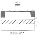
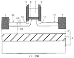
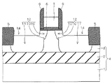
図1は、本発明の実施の形態1に係る半導体装置の構造を示す断面図である。SOI基板4は、シリコン基板1、BOX(buried oxide)層2、及びp型のシリコン層3がこの順に積層された構造を有している。シリコン層3の上面内には、いわゆる部分分離型の素子分離絶縁膜5が部分的に形成されている。素子分離絶縁膜5の材質は、例えばシリコン酸化膜である。素子分離絶縁膜5の底面とBOX層2の上面とによって、シリコン層3の一部が挟まれている。
FIG. 1 is a sectional view showing a structure of the semiconductor device according to the first embodiment of the present invention. The
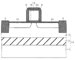
素子分離絶縁膜5によって規定される素子形成領域内において、シリコン層3の上面上には、ゲート構造が部分的に形成されている。ゲート構造は、シリコン層3の上面上に形成された、シリコン酸化膜から成るゲート絶縁膜6と、ゲート絶縁膜6上に形成された、ポリシリコンから成るゲート電極7と、ゲート電極7の側面に形成された、シリコン窒化膜から成るサイドウォール9と、ゲート電極7の上面上に形成されたコバルトシリサイド層8とを有している。ゲート構造の下方に位置する部分のシリコン層3は、チャネル形成領域として規定される。ここで、各部の材質は、上記の例に限定されるものではない。ゲート絶縁膜6の材質は、シリコン酸窒化膜又は高誘電体膜等であっても良い。ゲート電極7の材質は、タングステン、アルミニウム、又はタンタル等の金属であっても良い。サイドウォール9の材質は、シリコン酸化膜とシリコン窒化膜との複合膜であっても良い。コバルトシリサイド層8の代わりに、ニッケルシリサイド層又はチタンシリサイド層等が形成されていても良い。
In the element formation region defined by the element isolation
素子形成領域内において、ゲート構造から露出している部分のシリコン層3の上面内には、チャネル形成領域を挟んで対を成す凹部14が形成されている。また、シリコン層3内には、チャネル形成領域を挟んで対を成す、n型のソース・ドレイン領域12が形成されている。ソース・ドレイン領域12は、シリコン層3の上面内に浅く形成された、比較的低濃度の不純物導入領域(「エクステンション」とも称される)10と、不純物導入領域10よりも深く形成された、比較的高濃度の不純物導入領域11とを有している。不純物導入領域11は、凹部14の底面からBOX層2の上面に到達して形成されている。また、ゲート構造から露出している部分のソース・ドレイン領域12の上面上には、コバルトシリサイド層13が形成されている。
In the element formation region, a pair of
図1には、不純物導入領域11の底面がBOX層2の上面に接触している構造を示したが、この構造の代わりに、不純物導入領域11とシリコン層3との界面に形成される空乏層が、BOX層2の上面に到達する構造が採用されても良い。但し、接合容量の低減を図る観点からは、不純物導入領域11の底面がBOX層2の上面に接触している構造が望ましいため、本明細書では、この構造が採用された場合について説明する。
FIG. 1 shows a structure in which the bottom surface of
図2〜8は、本実施の形態1に係る半導体装置の製造方法を工程順に示す断面図である。図2を参照して、周知のLOCOS分離技術又はトレンチ分離技術によって、素子分離絶縁膜5をシリコン層3の上面内に部分的に形成する。次に、熱酸化法によって、シリコン酸化膜15をシリコン層3の上面上に形成する。次に、CVD法によって、ポリシリコン膜16及びシリコン酸化膜17をこの順に全面的に形成する。
2 to 8 are cross-sectional views illustrating a method of manufacturing the semiconductor device according to the first embodiment in the order of steps. Referring to FIG. 2, element
図3を参照して、次に、写真製版法及び異方性ドライエッチング法によって、ポリシリコン膜16及びシリコン酸化膜17をパターニングする。これにより、ポリシリコン膜19及びシリコン酸化膜20が形成される。また、シリコン酸化膜15の一部がエッチングされて、シリコン酸化膜18が形成される。
Referring to FIG. 3, next,
図4を参照して、次に、イオン注入法によって、n型の不純物をシリコン酸化膜18を介してシリコン層3の上面内に注入することにより、不純物導入領域10を形成する。このとき、ショートチャネル効果を抑制するために、比較的低濃度のp型の不純物層(一般的に「ポケット領域」と称される)を形成しても良い。但し、説明の簡略化のため、以後の説明ではポケット領域については省略する。
Referring to FIG. 4, next, an
図5を参照して、次に、CVD法によってシリコン窒化膜を全面的に形成する。次に、エッチバックを行うことにより、ポリシリコン膜19及びシリコン酸化膜20の側面にサイドウォール9を形成する。
Next, referring to FIG. 5, a silicon nitride film is entirely formed by the CVD method. Next,
図6を参照して、次に、シリコン酸化膜はエッチングされやすく、シリコン、ポリシリコン、及びシリコン窒化膜はエッチングされにくい条件で、エッチングを行う。これにより、シリコン酸化膜20が除去されて、ポリシリコン膜19の上面が露出する。また、サイドウォール9及びポリシリコン膜19から露出している部分のシリコン酸化膜18が除去されて、ゲート絶縁膜6が形成される。なお、図面には現さないが、このエッチングによって素子分離絶縁膜5も若干エッチングされる。
Referring to FIG. 6, next, etching is performed under conditions that the silicon oxide film is easily etched and the silicon, polysilicon, and silicon nitride films are hardly etched. Thereby,
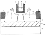
図7を参照して、次に、シリコン及びポリシリコンはエッチングされやすく、シリコン酸化膜及びシリコン窒化膜はエッチングされにくい条件で、異方性ドライエッチングを行う。これにより、ゲート絶縁膜6及び素子分離絶縁膜5から露出している部分のシリコン層3が膜厚D1だけエッチングされて、凹部14が形成される。また、ポリシリコン膜19の上部が併せてエッチングされて、ゲート電極7が形成される。凹部14の底面とBOX層2の上面とによって挟まれている部分のシリコン層3の膜厚は、D2である。
Referring to FIG. 7, next, anisotropic dry etching is performed under the condition that silicon and polysilicon are easily etched and the silicon oxide film and the silicon nitride film are hardly etched. As a result, the
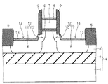
図8を参照して、次に、イオン注入法によって、n型の不純物をシリコン層3の上面内に注入することにより、不純物導入領域11を形成する。このイオン注入の注入エネルギーは、凹部14の底面に注入された不純物がシリコン層3の底面にまで到達し、かつ、素子分離絶縁膜5の上面に注入された不純物が素子分離絶縁膜5を突き抜けない大きさに設定される。
Referring to FIG. 8, next, an n-type impurity is implanted into the upper surface of
また、このイオン注入によって、n型の不純物はゲート電極7内にも併せて注入される。ポリシリコン膜19が薄膜化されてゲート電極7が形成されているため、不純物はゲート電極7の深部、即ちゲート絶縁膜6との界面付近にまで到達する。その結果、ゲート空乏化を抑制することができる。ゲート空乏化を抑制することによって、電流駆動能力を向上できる。
Further, by this ion implantation, an n-type impurity is also implanted into the
その後、ゲート電極7及びソース・ドレイン領域12の各上面をシリサイド化してコバルトシリサイド層8,13を形成することにより、図1に示した構造が得られる。
Thereafter, the upper surfaces of the
このように本実施の形態1に係る半導体装置及びその製造方法によると、凹部14を形成することによってシリコン層3が予め薄膜化された後に、イオン注入法によって不純物導入領域11が形成される。従って、素子分離絶縁膜5の底面とBOX層2の上面との間に位置する部分のp型のシリコン層3内に、n型の不純物が注入されないため、分離耐圧が低下することを回避できる。しかも、不純物導入領域11はBOX層2の上面に到達して形成されるため、ソース・ドレイン領域12の接合容量が増加することもない。
As described above, according to the semiconductor device and the method of manufacturing the same according to the first embodiment, after the
また、凹部14を形成するためのドライエッチングによって、シリコン層3内に欠陥が形成される。この欠陥はライフタイムキラーとして機能するため、SOI基板を用いた半導体装置に特有の問題である、基板フローティング効果の発生を抑制することもできる。
Further, a defect is formed in the
なお、本実施の形態1ではNMOSトランジスタを例にとり説明したが、PMOSトランジスタの場合であっても、あるいはNMOSトランジスタとPMOSトランジスタとが混載されたCMOSトランジスタの場合であっても、上記と同様の効果を得ることができる。後述の他の実施の形態についても同様である。 Although the first embodiment has been described by taking an NMOS transistor as an example, the same applies to the case of a PMOS transistor or a CMOS transistor in which an NMOS transistor and a PMOS transistor are mixed. The effect can be obtained. The same applies to other embodiments described later.
実施の形態2.
図9は、本発明の実施の形態2に係る半導体装置の構造を示す断面図である。サイドウォール9の底面は、ゲート絶縁膜6の底面よりも下方に位置している。即ち、サイドウォール9が形成されている部分のシリコン層3の膜厚は、ゲート絶縁膜6が形成されている部分のシリコン層3の膜厚よりも薄い。
FIG. 9 is a sectional view showing the structure of the semiconductor device according to the second embodiment of the present invention. The bottom surface of the
図10〜15は、本実施の形態2に係る半導体装置の製造方法を工程順に示す断面図である。まず、上記実施の形態1と同様の方法により、図2に示した構造を得る。 10 to 15 are sectional views showing a method of manufacturing a semiconductor device according to the second embodiment in the order of steps. First, the structure shown in FIG. 2 is obtained by the same method as in the first embodiment.
図10を参照して、次に、写真製版法及び異方性ドライエッチング法によって、シリコン酸化膜15、ポリシリコン膜16、及びシリコン酸化膜17をパターニングする。これにより、ゲート絶縁膜6、ポリシリコン膜19、及びシリコン酸化膜20が形成される。また、オーバーエッチングによって、ゲート絶縁膜6及び素子分離絶縁膜5から露出している部分のシリコン層3を膜厚D3だけエッチングすることにより、凹部21を形成する。
Referring to FIG. 10, next,
図11を参照して、次に、イオン注入法によって、n型の不純物をシリコン層3の上面内に注入することにより、不純物導入領域10を形成する。不純物導入領域10は、凹部21の底面内に形成される。不純物導入領域10を形成するためのイオン注入の注入エネルギーは、本実施の形態2と上記実施の形態1とで同一である。
Referring to FIG. 11, next, an
図12を参照して、次に、CVD法によってシリコン窒化膜を全面的に形成した後にエッチバックを行うことにより、サイドウォール9を形成する。サイドウォール9は、ゲート絶縁膜6、ポリシリコン膜19、及びシリコン酸化膜20の各側面に接して、凹部21の底面上に形成されている。
Referring to FIG. 12, next, a silicon nitride film is entirely formed by the CVD method, and then etch back is performed to form
図13を参照して、次に、シリコン酸化膜はエッチングされやすく、シリコン、ポリシリコン、及びシリコン窒化膜はエッチングされにくい条件で、エッチングを行う。これにより、シリコン酸化膜20が除去されて、ポリシリコン膜19の上面が露出する。
Referring to FIG. 13, next, etching is performed under the condition that the silicon oxide film is easily etched and the silicon, polysilicon, and silicon nitride films are hardly etched. Thereby,
図14を参照して、次に、シリコン及びポリシリコンはエッチングされやすく、シリコン酸化膜及びシリコン窒化膜はエッチングされにくい条件で、異方性ドライエッチングを行う。これにより、サイドウォール9、ゲート絶縁膜6、及び素子分離絶縁膜5から露出している部分のシリコン層3が膜厚D1だけエッチングされて、凹部14が形成される。また、ポリシリコン膜19の上部が併せてエッチングされて、ゲート電極7が形成される。凹部14の底面とBOX層2の上面とによって挟まれている部分のシリコン層3の膜厚D4は、図7に示した膜厚D2よりも、膜厚D3分だけ薄い。
Referring to FIG. 14, next, anisotropic dry etching is performed under the condition that silicon and polysilicon are easily etched and the silicon oxide film and the silicon nitride film are hardly etched. As a result, the
図15を参照して、次に、上記実施の形態1と同様に、n型の不純物をシリコン層3の上面内にイオン注入することにより、不純物導入領域11を形成する。上記の通り、本実施の形態2に係るシリコン層3の膜厚D4は、上記実施の形態1に係るシリコン層3の膜厚D2よりも薄い。従って、本実施の形態2においては、不純物導入領域11を形成するためのイオン注入の注入エネルギーを、上記実施の形態1よりも下げることができる。
Referring to FIG. 15, next, as in the first embodiment, an n-type impurity is ion-implanted into the upper surface of
その後、ゲート電極7及びソース・ドレイン領域12の各上面をシリサイド化してコバルトシリサイド層8,13を形成することにより、図9に示した構造が得られる。
Thereafter, the upper surfaces of the
このように本実施の形態2に係る半導体装置及びその製造方法によると、不純物導入領域11を形成するためのイオン注入の注入エネルギーを、上記実施の形態1よりも下げることができる。そのため、素子分離絶縁膜5の上面に注入された不純物が素子分離絶縁膜5を突き抜けることを、上記実施の形態1よりも確実に回避することができる。
As described above, according to the semiconductor device and the method of manufacturing the same according to the second embodiment, the implantation energy of the ion implantation for forming the impurity-doped
図16は、本実施の形態2の変形例に係る半導体装置の製造方法の一工程を示す断面図である。図14に示した工程ではシリコン層3が膜厚D1だけエッチングされたが、図16に示すように、膜厚D5(<D1)だけシリコン層3をエッチングすることによって、凹部22を形成してもよい。凹部22の底面とBOX層2の上面とによって挟まれている部分のシリコン層3の膜厚は、図7に示した膜厚D2に等しい。
FIG. 16 is a cross-sectional view showing one step of a method for manufacturing a semiconductor device according to a modification of the second embodiment. In the step shown in FIG. 14, the
このように本実施の形態2の変形例に係る半導体装置及びその製造方法によると、対を成す不純物導入領域11同士の間隔を、上記実施の形態1と同程度に保つことができる。そのため、図9に示した構造と比較して、ショートチャネル効果の影響を抑制することができる。
As described above, according to the semiconductor device and the method for manufacturing the same according to the modification of the second embodiment, the interval between the
また、上記実施の形態1と比較して、不純物導入領域10が膜厚D3分だけ深くに形成される。そのため、不純物導入領域10と不純物導入領域11とが互いに重なり合う度合いを、上記実施の形態1よりも大きくできる。その結果、ソース・ドレイン領域12の寄生抵抗を、上記実施の形態1よりも低減することが可能となる。
Further, as compared with the first embodiment,
実施の形態3.
図17,18は、図7に示した構造のうち、凹部14が形成されている付近の構造を拡大して示す断面図である。図17を参照して、ゲート絶縁膜6が形成されている部分のシリコン層3の上面と、凹部14の側面とが成す角度αは、90°よりも大きい。角度αは、Cl2やHBr等のエッチングガスに添加するO2ガスの量によって調整することができる。
FIGS. 17 and 18 are cross-sectional views showing, on an enlarged scale, the structure around the
このように角度αを90°よりも大きく設定することにより、図1に示した構造において、コバルトシリサイド層13とチャネル形成領域との間の距離を、比較的長く保つことができる。その結果、コバルトシリサイド層13とチャネル形成領域との間に流れる接合リーク電流を低減することができる。
By setting the angle α to be larger than 90 °, the distance between the
また、図17を参照して、シリコン層3の上面から凹部14の底面までの深さ(膜厚D1)は、シリコン層3の上面から不純物導入領域10の底面までの深さD6よりも浅い。
凹部14の深さは、エッチング時間によって調整することができる。
Referring to FIG. 17, the depth (film thickness D1) from the upper surface of
The depth of the
このようにD1<D6に設定することにより、凹部14の形成に起因して不純物導入領域10の寄生抵抗が増加することを、抑制することができる。
By setting D1 <D6 in this manner, an increase in the parasitic resistance of the impurity-doped
図18を参照して、凹部14の端部は、ゲート絶縁膜6の端部の下方に潜り込んでいても良い。例えば、等方性エッチングによってシリコン層3をエッチングすることにより、かかる構造を得ることができる。
With reference to FIG. 18, the end of
このようにゲート構造の端部の下方に潜り込むように凹部14を形成することにより、ライフタイムキラーとして機能する欠陥を、よりチャネル形成領域に近付けて形成することができる。その結果、基板フローティング効果の発生を、より効果的に抑制することができる。
By forming the
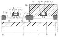
実施の形態4.
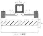
図19は、本発明の実施の形態4に係る半導体装置の構造を示す断面図である。SOI基板4内には、NMOSトランジスタとPMOSトランジスタとが形成されている。NMOSトランジスタは、p型のシリコン層31、ゲート絶縁膜61、ゲート電極71、コバルトシリサイド層81,131、サイドウォール91、及びn型のソース・ドレイン領域121を備えている。ソース・ドレイン領域121は、不純物導入領域101,111を有している。NMOSトランジスタに関しては、上記実施の形態1と同様に、凹部141の底面内にソース・ドレイン領域121が形成された構造(以下、本明細書において「リセスソース・ドレイン構造」と称する)が採用されている。
FIG. 19 is a sectional view showing the structure of the semiconductor device according to the fourth embodiment of the present invention. In the
上記実施の形態1で述べたように、リセスソース・ドレイン構造を採用すると、基板フローティング効果の発生を抑制することができる。一般的に、基板フローティング効果は、PMOSトランジスタよりもNMOSトランジスタのほうが問題となる。そのため、NMOSトランジスタにリセスソース・ドレイン構造を採用することにより、NMOSトランジスタに関して基板フローティング効果の発生を抑制することができる。 As described in the first embodiment, when the recess source / drain structure is employed, the occurrence of the substrate floating effect can be suppressed. Generally, the substrate floating effect is more problematic for NMOS transistors than for PMOS transistors. Therefore, by employing the recess source / drain structure for the NMOS transistor, the occurrence of the substrate floating effect with respect to the NMOS transistor can be suppressed.
また、リセスソース・ドレイン構造を採用すると、チャネル形成領域がコバルトシリサイド層131に引っ張られることによってシリコン層31の内部に発生する応力が、リセスソース・ドレイン構造が採用されていない場合よりも増加する。その結果、キャリアの移動度が増加するため、NMOSトランジスタにリセスソース・ドレイン構造を採用することにより、電流駆動能力を向上できる。
Further, when employing the Risesusosu drain structure, a channel formation region is stress generated in the interior of the
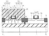
PMOSトランジスタは、n型のシリコン層32、ゲート絶縁膜62、ゲート電極72、コバルトシリサイド層82,132、サイドウォール92、及びp型のソース・ドレイン領域122を備えている。ソース・ドレイン領域122は、不純物導入領域102,112を有している。PMOSトランジスタに関しては、リセスソース・ドレイン構造が採用されておらず、従来の半導体装置と同様に、シリコン層32の上面内に不純物導入領域102,112が形成された、通常のソース・ドレイン構造が採用されている。
PMOS transistor, n-
リセスソース・ドレイン構造を採用しない場合は、リセスソース・ドレイン構造を採用した場合と比較すると、特にシリコン層3の深部において、対を成す不純物導入領域11同士の間隔を広げることができる。そのため、ショートチャネル効果の発生を抑制することができる。一般的に、ショートチャネル効果は、NMOSトランジスタよりもPMOSトランジスタのほうが問題となる。そのため、分離耐圧よりもトランジスタの性能が優先される場合には、PMOSトランジスタにリセスソース・ドレイン構造を採用しないことにより、PMOSトランジスタに関してショートチャネル効果を改善することができる。
In the case where the recess source / drain structure is not used, the distance between the
また、上記の通り、リセスソース・ドレイン構造を採用すると、チャネル形成領域がコバルトシリサイド層13に引っ張られることによってシリコン層3の内部に発生する応力が増加する。PMOSトランジスタに関しては、NMOSトランジスタとは逆に、上記応力が増加するとキャリアの移動度が低下してしまう。そのため、PMOSトランジスタにはリセスソース・ドレイン構造を採用しないことにより、電流駆動能力が低下することを回避できる。
As described above, when the recess source / drain structure is employed, the stress generated inside the
NMOSトランジスタとPMOSトランジスタとの間には、底面の一部がBOX層2の上面に到達する、いわゆる完全分離型の素子分離絶縁膜23が形成されている。これにより、NMOSトランジスタとPMOSトランジスタとは、互いに電気的に分離されている。この分離構造を用いることにより、ラッチアップを抑制することができる。この分離構造は、他の全ての実施の形態にも適用可能である。
Between the NMOS transistor and the PMOS transistor, a so-called complete isolation type element
図20〜27は、本実施の形態4に係る半導体装置の製造方法を工程順に示す断面図である。図20を参照して、熱酸化法によって、シリコン酸化膜15をシリコン層31,32の上面上に形成する。次に、CVD法によって、ポリシリコン膜16を全面的に形成する。
20 to 27 are sectional views showing a method of manufacturing a semiconductor device according to the fourth embodiment in the order of steps. Referring to FIG. 20, by thermal oxidation to form a
図21を参照して、次に、写真製版法及び異方性ドライエッチング法によって、ポリシリコン膜16をパターニングする。これにより、ポリシリコン膜191及びゲート電極72が形成される。また、シリコン酸化膜15の一部がエッチングされて、シリコン酸化膜181,182が形成される。
Referring to FIG. 21, next,
図22を参照して、次に、写真製版法及びイオン注入法によって、n型の不純物をシリコン酸化膜181を介してシリコン層31の上面内に注入することにより、不純物導入領域101を形成する。次に、写真製版法及びイオン注入法によって、p型の不純物をシリコン酸化膜182を介してシリコン層32の上面内に注入することにより、不純物導入領域102を形成する。
Referring to FIG. 22, then, by photolithography and ion implantation, by the n-type impurity is implanted into the
図23を参照して、次に、CVD法によってシリコン窒化膜を全面的に形成した後にエッチバックを行う。これにより、ポリシリコン膜191の側面にサイドウォール91が形成されるとともに、ゲート電極72の側面にサイドウォール92が形成される。また、ゲート絶縁膜61,62が形成される。
Referring to FIG. 23, an etch-back is performed after a silicon nitride film is entirely formed by the CVD method. Thus, together with the
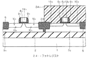
図24を参照して、次に、写真製版法によって、PMOSトランジスタの形成予定領域を覆ってフォトレジスト24を形成する。
Next, referring to FIG. 24, a
図25を参照して、次に、フォトレジスト24をエッチングマスクに用いて、シリコン及びポリシリコンはエッチングされやすく、シリコン酸化膜及びシリコン窒化膜はエッチングされにくい条件で、異方性ドライエッチングを行う。これにより、フォトレジスト24、ゲート絶縁膜61、及び素子分離絶縁膜5,23から露出している部分のシリコン層31がエッチングされて、凹部141が形成される。また、ポリシリコン膜191の上部が併せてエッチングされて、ゲート電極71が形成される。
Referring to FIG. 25, next, using
図26を参照して、次に、フォトレジスト24を注入マスクに用いて、イオン注入法によって、n型の不純物をシリコン層31の上面内に注入することにより、不純物導入領域111を形成する。n型の不純物は、ゲート電極71内にも注入される。その後、フォトレジスト24を除去する。
Referring to FIG. 26, then, formed by using a
図27を参照して、次に、写真製版法によって、NMOSトランジスタの形成予定領域を覆ってフォトレジスト25を形成する。次に、フォトレジスト25を注入マスクに用いて、イオン注入法によって、p型の不純物をシリコン層32の上面内に注入することにより、不純物導入領域112を形成する。p型の不純物は、ゲート電極72内にも注入される。その後、フォトレジスト25を除去する。
Next, referring to FIG. 27, a
その後、ゲート電極71,72及びソース・ドレイン領域121,122の各上面をシリサイド化してコバルトシリサイド層81,82,131,132を形成することにより、図19に示した構造が得られる。
After that, each upper surface of the
図28は、本実施の形態4の変形例に係る半導体装置の構造を示す断面図である。PMOSトランジスタに関しては、上記実施の形態1と同様に、凹部142の底面内にソース・ドレイン領域122が形成された、リセスソース・ドレイン構造が採用されている。
FIG. 28 is a cross-sectional view illustrating a structure of a semiconductor device according to a modification of the fourth embodiment. For the PMOS transistor, as in the first embodiment, the source-
上記実施の形態1で述べたように、リセスソース・ドレイン構造の採用によってゲートポリシリコンを薄膜化することにより、ゲート空乏化を抑制することができる。一般的に、ゲート空乏化は、NMOSトランジスタよりもPMOSトランジスタのほうが問題となる。そのため、PMOSトランジスタにリセスソース・ドレイン構造を採用することにより、PMOSトランジスタのゲート空乏化を効果的に抑制することができる。 As described in the first embodiment, the gate depletion can be suppressed by reducing the thickness of the gate polysilicon by adopting the recess source / drain structure. Generally, gate depletion is more problematic for PMOS transistors than for NMOS transistors. Therefore, by employing the recess source / drain structure in the PMOS transistor, the gate depletion of the PMOS transistor can be effectively suppressed.
NMOSトランジスタに関しては、リセスソース・ドレイン構造が採用されておらず、従来の半導体装置と同様に、通常のソース・ドレイン構造が採用されている。 As for the NMOS transistor, a recess source / drain structure is not adopted, and a normal source / drain structure is adopted like a conventional semiconductor device.
リセスソース・ドレイン構造を採用しない場合は、リセスソース・ドレイン構造を採用した場合と比較すると、ソース・ドレイン領域12の寄生抵抗が小さくなる。凹部14が形成されない分だけ、不純物導入領域102,112の面積の縮小を回避できるからである。一般的に、高速動作が要求されるロジック回路等においては、PMOSトランジスタよりもNMOSトランジスタが多用されている。NMOSトランジスタにリセスソース・ドレイン構造を採用しないことにより、ソース・ドレイン領域12の寄生抵抗の増加に起因して動作速度が低下することを、回避することができる。
When the recess source / drain structure is not used, the parasitic resistance of the source /
なお、図19,28では、NMOSトランジスタ及びPMOSトランジスタのうちのいずれか一方のみにリセスソース・ドレイン構造が採用されている場合を示したが、NMOSトランジスタ及びPMOSトランジスタの双方にリセスソース・ドレイン構造が採用されていても構わない。 Although FIGS. 19 and 28 show the case where the recess source / drain structure is used for only one of the NMOS transistor and the PMOS transistor, the recess source / drain structure is used for both the NMOS transistor and the PMOS transistor. It does not matter.
実施の形態5.
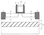
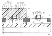
図29は、本発明の実施の形態5に係る半導体装置の構造を示す断面図である。SOI基板4内には、比較的低い電源電圧(例えば1.0V)で動作するMOSトランジスタ(以下「低電圧動作トランジスタ」と称する)と、比較的高い電源電圧(例えば3.3V)で動作するMOSトランジスタ(以下「高電圧動作トランジスタ)とが形成されている。低電圧動作トランジスタは、例えばCPUコアを構成するトランジスタである。高電圧動作トランジスタは、例えば入出力回路を構成するトランジスタである。
FIG. 29 is a sectional view showing the structure of the semiconductor device according to the fifth embodiment of the present invention. In the
低電圧動作トランジスタは、ゲート絶縁膜6、ゲート電極7、コバルトシリサイド層8,13、サイドウォール9、及びソース・ドレイン領域12を備えている。ソース・ドレイン領域12は、不純物導入領域10,11を有している。低電圧動作トランジスタに関しては、リセスソース・ドレイン構造が採用されている。
The low-voltage operation transistor includes a
リセスソース・ドレイン構造を採用することにより、低電圧動作トランジスタに関して、基板フローティング効果の発生や分離耐圧の低下を抑制することができる。 By employing the recess source / drain structure, it is possible to suppress the occurrence of the substrate floating effect and the reduction of the isolation withstand voltage for the low-voltage operation transistor.
高電圧動作トランジスタは、ゲート絶縁膜30、ゲート電極31、コバルトシリサイド層32,37、サイドウォール33、及びソース・ドレイン領域36を備えている。ソース・ドレイン領域36は、不純物導入領域34,35を有している。高電圧動作トランジスタに関しては、リセスソース・ドレイン構造が採用されていない。
The high-voltage operation transistor includes a
一例として、低電圧動作トランジスタのゲート長が80nm程度であるのに対して、高電圧動作トランジスタのゲート長は0.4μm程度である。即ち、高電圧動作トランジスタは、低電圧動作トランジスタよりもゲート長が長い。従って、高電圧動作トランジスタに関しては、素子分離絶縁膜5の上面とシリコン層3の上面との段差が大きくなるように素子分離絶縁膜5の膜厚を厚くすることによって、分離耐圧の低下を抑制することができる。上記段差に起因してゲート電極31の寸法に変動が生じたとしても、そもそもゲート長が長いため、寸法の変動が動作速度の低下や特性のばらつきに及ぼす影響が少ないからである。
As an example, the gate length of the low-voltage operation transistor is about 80 nm, while the gate length of the high-voltage operation transistor is about 0.4 μm. That is, the high voltage operation transistor has a longer gate length than the low voltage operation transistor. Therefore, with respect to the high-voltage operation transistor, a decrease in the isolation breakdown voltage is suppressed by increasing the thickness of the element
また、SOI基板4の上面のうち入出力回路が占める面積は、CPUコアが占める面積よりも十分に小さい。従って、入出力回路に関してデザインルールを大きく設定したとしても、ICチップの大型化に対する影響は比較的少ない。デザインルールを大きく設定すると、素子分離絶縁膜5の分離長も長くなるため、リセスソース・ドレイン構造を採用するまでもなく、所望の分離耐圧を確保できる。
The area occupied by the input / output circuits on the upper surface of the
以上のように、素子分離絶縁膜5の膜厚を厚くしたり、デザインルールを大きく設定することができる場合は、高電圧動作トランジスタに関してリセスソース・ドレイン構造を採用することなく、低電圧動作トランジスタに関してのみ採用することが可能である。上記の通り、リセスソース・ドレイン構造を採用しないことにより、寄生抵抗の増加に起因する動作速度の低下を回避することができる。
As described above, in the case where the thickness of the element
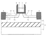
図30は、本実施の形態5の変形例に係る半導体装置の構造を示す断面図である。高電圧動作トランジスタに関しては、凹部38の底面内にソース・ドレイン領域36が形成された、リセスソース・ドレイン構造が採用されている。
FIG. 30 is a cross-sectional view showing a structure of a semiconductor device according to a modification of the fifth embodiment. As for the high voltage operation transistor, a recess source / drain structure in which the source /
入出回路に関して、素子分離絶縁膜5の膜厚を厚くしたり、デザインルールを大きく設定することができない場合もある。このような場合、高電圧動作トランジスタについては、低電圧動作トランジスタよりも高い分離耐圧が要求される。高電圧動作トランジスタには、低電圧動作トランジスタよりも高い電源電圧が印加されるからである。従って、このような場合は高電圧動作トランジスタにリセスソース・ドレイン構造を採用することによって、分離耐圧を高めることができる。
Regarding the input / output circuit, it may not be possible to increase the thickness of the element
一方、低電圧動作トランジスタに関しては、リセスソース・ドレイン構造が採用されておらず、通常のソース・ドレイン構造が採用されている。 On the other hand, the low-voltage operation transistor does not employ a recess source / drain structure, but employs a normal source / drain structure.
上記の通り、リセスソース・ドレイン構造を採用しない場合は、凹部14が形成されない分だけソース・ドレイン領域12の寄生抵抗が小さくなる。従って、高速動作が要求されるCPUコアにおいては、低電圧動作トランジスタにリセスソース・ドレイン構造を採用しないことにより、寄生抵抗の増加に起因する動作速度の低下を回避することができる。
As described above, when the recess source / drain structure is not adopted, the parasitic resistance of the source /
なお、図29,30では、低電圧動作トランジスタ及び高電圧動作トランジスタのうちのいずれか一方のみにリセスソース・ドレイン構造が採用されている場合を示したが、低電圧動作トランジスタ及び高電圧動作トランジスタの双方にリセスソース・ドレイン構造が採用されていても構わない。 Although FIGS. 29 and 30 show the case where only one of the low-voltage operation transistor and the high-voltage operation transistor employs the recess source / drain structure, the low-voltage operation transistor and the high-voltage operation transistor have the same structure. A recess source / drain structure may be adopted for both.
低電圧動作トランジスタ及び高電圧動作トランジスタのうちのいずれか一方のみにリセスソース・ドレイン構造を採用したい場合には、上記実施の形態4と同様に、フォトレジスト24,25を用いて、ソース・ドレイン領域の構造を作り分ければよい。
When it is desired to adopt the recessed source / drain structure for only one of the low-voltage operation transistor and the high-voltage operation transistor, the
また、NMOS構造の低電圧トランジスタとPMOS構造の低電圧トランジスタとが混在している場合に、上記実施の形態4と同様に、NMOS及びPMOSの一方のトランジスタのみにリセスソース・ドレイン構造を採用しても良い。NMOS構造の高電圧トランジスタとPMOS構造の高電圧動作トランジスタとが混在している場合についても同様である。 Further, in the case where the low voltage transistor having the NMOS structure and the low voltage transistor having the PMOS structure coexist, the recess source / drain structure is employed only for one of the NMOS and PMOS transistors as in the fourth embodiment. Is also good. The same applies to a case where a high-voltage transistor having an NMOS structure and a high-voltage operation transistor having a PMOS structure are mixed.
実施の形態6.
図31は、本発明の実施の形態6に係る半導体装置の製造方法の一工程を示す断面図である。上記実施の形態1等では、ポリシリコン膜19上に形成されたシリコン酸化膜20が除去された後に、凹部14を形成するためのエッチングが行われた。そのため、図7に示したように、エッチングによってポリシリコン膜19が薄膜化された結果として、ゲート電極7が形成された。
FIG. 31 is a cross-sectional view showing a step of a method for manufacturing a semiconductor device according to the sixth embodiment of the present invention. In the first embodiment and the like, after the
これに対し本実施の形態6では、図31に示すように、ポリシリコン膜19上に、シリコン酸化膜20ではなくシリコン窒化膜40を形成する。すると、図6に示した工程でシリコン窒化膜40がエッチングされないため、凹部14を形成するためのエッチング工程において、シリコン窒化膜40がエッチングマスクとして機能することにより、ポリシリコン膜19はエッチングされない。従って、ポリシリコン膜19がそのままゲート電極となる。
In contrast, in the sixth embodiment, as shown in FIG. 31, a
不純物導入領域11を形成するためのイオン注入工程(図8)において、シリコン窒化膜40を介してポリシリコン膜19内にも不純物がイオン注入される。
In the ion implantation step for forming the impurity introduction region 11 (FIG. 8), impurities are also ion-implanted into the
このように本実施の形態6に係る半導体装置及びその製造方法によると、上記実施の形態1と比較してゲート電極の膜厚が厚くなる。従って、不純物導入領域11を形成するためのイオン注入工程において、ポリシリコン膜19内に注入された不純物がポリシリコン膜19を突き抜けて、ゲート絶縁膜6やチャネル形成領域にまで到達することを抑制できる。その結果、不純物の突き抜けに起因するしきい値電圧の変動を、抑制することができる。
As described above, according to the semiconductor device and the method of manufacturing the same according to the sixth embodiment, the thickness of the gate electrode is larger than that of the first embodiment. Therefore, in the ion implantation step for forming the
また、ポリシリコン膜19の膜厚がそのままゲート電極の膜厚となるため、上記実施の形態1等と比較して、ゲート電極の膜厚制御が容易となる。
Further, since the thickness of the
本実施の形態6に係るリセスソース・ドレイン構造は、他の全ての実施の形態にも適用することができる。 The recess source / drain structure according to the sixth embodiment can be applied to all the other embodiments.
実施の形態7.
図32,33は、本発明の実施の形態7に係る半導体装置の製造方法を工程順に示す断面図である。図32を参照して、図31に示す構造を得た後、CVD法によって、シリコン窒化膜又はシリコン酸化膜を全面に形成する。次に、そのシリコン窒化膜又はシリコン酸化膜をエッチバックすることにより、サイドウォール41,42を形成する。サイドウォール41は、サイドウォール9の側面に接して、凹部14の底面上に形成されている。サイドウォール42は、素子分離絶縁膜5の側面に接して、凹部14の底面上に形成されている。
32 and 33 are sectional views illustrating a method of manufacturing a semiconductor device according to the seventh embodiment of the present invention in the order of steps. Referring to FIG. 32, after obtaining the structure shown in FIG. 31, a silicon nitride film or a silicon oxide film is formed on the entire surface by a CVD method. Next, the silicon nitride film or silicon oxide film is etched back to
図33を参照して、次に、イオン注入法によって不純物導入領域11を形成する。次に、ソース・ドレイン領域12の上面をシリサイド化することにより、コバルトシリサイド層43を形成する。コバルトシリサイド層43は、サイドウォール41,42から露出している部分の凹部14の底面上に形成されている。
Referring to FIG. 33, next,
なお、以上の説明では、上記実施の形態6を基礎として本実施の形態7に係る半導体装置の製造方法について述べたが、本実施の形態7に係る発明は、他の全ての実施の形態に適用することができる。 In the above description, the method for manufacturing a semiconductor device according to the seventh embodiment is described based on the sixth embodiment. However, the invention according to the seventh embodiment is applicable to all other embodiments. Can be applied.
また、サイドウォール41を形成した後に不純物導入領域11を形成したが、これとは逆に、不純物導入領域11を形成した後にサイドウォール41を形成してもよい。
Further, although the
さらに、素子分離絶縁膜5の上面と凹部14の底面との段差が小さい場合には、サイドウォール42が形成されないこともある。
Further, when the step between the top surface of the element
また、本実施の形態7に係る半導体装置の製造方法が、シリサイドプロテクション膜の形成工程(シリサイドプロテクション工程)を備える場合には、シリサイドプロテクション膜の一部としてサイドウォール41,42を形成してもよい。シリサイドプロテクション工程は、シリサイド化されないことによって高抵抗のポリシリコン膜を形成する工程である。シリサイドプロテクション工程においてサイドウォール41,42を併せて形成することにより、製造工程数の増加を防止することができる。
In the case where the method of manufacturing a semiconductor device according to the seventh embodiment includes a step of forming a silicide protection film (silicide protection step), sidewalls 41 and 42 may be formed as part of the silicide protection film. Good. The silicide protection step is a step of forming a high-resistance polysilicon film by not being silicided. By forming the
このように本実施の形態7に係る半導体装置及びその製造方法によると、サイドウォール41が形成されることに起因して、コバルトシリサイド層43とチャネル形成領域との間の距離が長くなる。その結果、コバルトシリサイド層43とチャネル形成領域との間に流れる接合リーク電流を低減することができる。
As described above, according to the semiconductor device and the method of manufacturing the same according to the seventh embodiment, the distance between
また、サイドウォール42が形成されることに起因して、コバルトシリサイド層43と、素子分離絶縁膜5の下方に位置する部分のシリコン層3との間の距離が長くなる。その結果、コバルトシリサイド層43と、この部分のシリコン層3との間に流れる接合リーク電流を低減することができる。
Further, due to the formation of the
実施の形態8.
図34,35は、本発明の実施の形態8に係る半導体装置の製造方法を工程順に示す断面図である。図34を参照して、図8に示す構造を得た後、選択的エピタキシャル成長法によって、ゲート電極7上及びソース・ドレイン領域12上に、シリコン層50,51をそれぞれ形成する。次に、イオン注入法によって、シリコン層50,51内にn型の不純物を高濃度で注入する。
34 and 35 are sectional views showing a method of manufacturing a semiconductor device according to the eighth embodiment of the present invention in the order of steps. Referring to FIG. 34, after obtaining the structure shown in FIG. 8, silicon layers 50 and 51 are formed on
図35を参照して、次に、シリコン層50,51の各上面をシリサイド化することにより、コバルトシリサイド層52,53を形成する。シリコン層50,51内にn型の不純物が注入されているため、シリコン層50,51とコバルトシリサイド層52,53との接触抵抗は低減されている。 Referring to FIG. 35, next, cobalt silicide layers 52 and 53 are formed by siliciding the upper surfaces of silicon layers 50 and 51, respectively. Since n-type impurities are implanted in silicon layers 50 and 51, the contact resistance between silicon layers 50 and 51 and cobalt silicide layers 52 and 53 is reduced.
このように本実施の形態8に係る半導体装置及びその製造方法によると、コバルトシリサイド層53は、ソース・ドレイン領域12上に形成されたシリコン層51上に形成されている。従って、コバルトシリサイド層53とチャネル形成領域との間の距離が長くなるため、両者間に流れる接合リーク電流を低減することができる。
As described above, according to the semiconductor device and the method of manufacturing the same according to the eighth embodiment,
実施の形態9.
図36〜38は、本発明の実施の形態9に係る半導体装置の製造方法を工程順に示す断面図である。図36を参照して、図4に示す構造を得た後、CVD法によって、シリコン窒化膜60を全面的に形成する。次に、写真製版法によって、素子分離絶縁膜5の上方に位置する部分のシリコン窒化膜60上に、フォトレジスト61を形成する。
36 to 38 are sectional views showing a method of manufacturing a semiconductor device according to the ninth embodiment of the present invention in the order of steps. Referring to FIG. 36, after obtaining the structure shown in FIG. 4, a
図37を参照して、次に、フォトレジスト61をエッチングマスクに用いて、異方性ドライエッチング法によってシリコン窒化膜60をエッチバックする。これにより、サイドウォール9が形成されるとともに、素子分離絶縁膜5上にシリコン窒化膜62が形成される。次に、フォトレジスト61を除去する。
Referring to FIG. 37, the
図38を参照して、次に、シリコン酸化膜20と、サイドウォール9及びポリシリコン膜19から露出している部分のシリコン酸化膜18とを除去する。次に、ゲート絶縁膜6及び素子分離絶縁膜5から露出している部分のシリコン層3をエッチングすることにより、凹部14を形成する。また、ポリシリコン膜19の上部を併せてエッチングすることにより、ゲート電極7を形成する。その後は、図8に示した工程以降の工程が順に実行される。
Referring to FIG. 38, the
このように本実施の形態9に係る半導体装置及びその製造方法によると、素子分離絶縁膜5上にシリコン窒化膜62が形成された構造と、リセスソース・ドレイン構造とを組み合わせることにより、分離耐圧の低下を効果的に抑制することが可能となる。即ち、サイドウォール9を形成する工程において、シリコン窒化膜62が素子分離絶縁膜5上に併せて形成されることにより、実質的に素子分離絶縁膜5の膜厚が厚くなる。そのため、不純物導入領域11を形成するためのイオン注入工程において、n型の不純物が素子分離絶縁膜5を突き抜けてシリコン層3内に注入されることを、さらに抑制することができる。
As described above, according to the semiconductor device and the method of manufacturing the same according to the ninth embodiment, by combining the structure in which the
なお、図37には、全体が素子分離絶縁膜5上に形成された、幅狭のシリコン窒化膜62を示したが、端部がシリコン酸化膜18上に形成された、幅広のシリコン窒化膜62を形成しても良い。この場合、不純物導入領域11の面積が小さくなるため、接合容量を低減することができる。
Although FIG. 37 shows the narrow
実施の形態10.
図39は、本発明の実施の形態10に係る半導体装置の構造を示す断面図である。図1に示した上記実施の形態1に係る半導体装置を基礎として、n型の不純物導入領域70が、シリコン層3の上面内にさらに形成されている。すなわち、ソース・ドレイン領域12は、いずれもn型の不純物導入領域10,11,70を有している。
FIG. 39 is a cross sectional view showing a structure of a semiconductor device according to the tenth embodiment of the present invention. On the basis of the semiconductor device according to the first embodiment shown in FIG. 1, an n-type
図40,41は、本実施の形態10に係る半導体装置の第1の製造方法を工程順に示す断面図である。まず、上記実施の形態1と同様の方法により、図6に示した構造を得る。 40 and 41 are sectional views showing a first manufacturing method of the semiconductor device according to the tenth embodiment in the order of steps. First, the structure shown in FIG. 6 is obtained by the same method as in the first embodiment.
図40を参照して、次に、イオン注入法によって、エネルギーが1〜30KeV程度、濃度が1×10¹⁵/cm2程度の条件で、ヒ素等のn型の不純物をシリコン層3の上面内に注入することにより、不純物導入領域70を形成する。
Referring to FIG. 40, next, an n-type impurity such as arsenic is implanted in the upper surface of
図41を参照して、次に、シリコン及びポリシリコンはエッチングされやすく、シリコン酸化膜及びシリコン窒化膜はエッチングされにくい条件で、異方性ドライエッチングを行う。これにより、ゲート絶縁膜6及び素子分離絶縁膜5から露出している部分のシリコン層3が膜厚D1だけエッチングされて、凹部14が形成される。また、ポリシリコン膜19の上部が併せてエッチングされて、ゲート電極7が形成される。その後、図8に示した工程以降の工程が実行されて、半導体装置が完成する。
Referring to FIG. 41, next, anisotropic dry etching is performed under the condition that silicon and polysilicon are easily etched and the silicon oxide film and the silicon nitride film are hardly etched. As a result, the
図42は、図41に示した構造のうち、凹部14が形成されている付近の構造を拡大して示す断面図である。シリコン層3の上面から不純物導入領域70の底面までの深さD7は、シリコン層3の上面から不純物導入領域10の底面までの深さD6よりも深い。また、シリコン層3の上面から凹部14の底面までの深さ(膜厚D1)は、深さD7よりも浅い。図41に示した工程では、膜厚D1が深さD7未満となるように、エッチングが制御される。なお、図42には、膜厚D1が深さD6未満である構造を示したが、本実施の形態10において、膜厚D1は深さD6以上であってもよい。
FIG. 42 is an enlarged cross-sectional view of the structure shown in FIG. 41 near the portion where the
図43,44は、本実施の形態10に係る半導体装置の第2の製造方法を工程順に示す断面図である。まず、上記実施の形態1と同様の方法により、図7に示した構造を得る。 43 and 44 are sectional views showing a second method of manufacturing the semiconductor device according to the tenth embodiment in the order of steps. First, the structure shown in FIG. 7 is obtained by the same method as in the first embodiment.
図43を参照して、次に、イオン注入法によって、エネルギーが1〜30KeV程度、濃度が1×10¹⁵/cm2程度の条件で、ヒ素等のn型の不純物71をシリコン層3内に注入することにより、不純物導入領域70を形成する。不純物71の注入方向は、SOI基板4の上面の法線方向に対して、30°程度傾斜している。
Referring to FIG. 43, next, an n-
図44を参照して、次に、図8に示した工程と同様に、n型の不純物をシリコン層3の上面内にイオン注入することにより、不純物導入領域11を形成する。その後、ゲート電極7及びソース・ドレイン領域12の各上面をシリサイド化することにより、半導体装置が完成する。
Referring to FIG. 44, next, similarly to the step shown in FIG. 8, an n-type impurity is ion-implanted into the upper surface of
このように本実施の形態10に係る半導体装置及びその製造方法によると、凹部14の形成に起因してソース・ドレイン領域12の寄生抵抗が増加することを、不純物導入領域70を追加することによってさらに抑制することができる。
As described above, according to the semiconductor device and the method of manufacturing the same according to the tenth embodiment, the increase in the parasitic resistance of source /
また、図41に示した工程では膜厚D1が深さD6ではなく深さD7未満となるようにエッチングが制御されるため、上記実施の形態1よりも凹部14を深く形成することができる。そのため、不純物導入領域11の形成工程(図8,44)におけるイオン注入の注入エネルギーを、上記実施の形態1よりも低く設定することができる。従って、素子分離絶縁膜5の底面とBOX層2の上面との間に位置する部分のp型のシリコン層3内にn型の不純物が注入されることを、上記実施の形態1よりも確実に回避でき、その結果、分離耐圧が低下することをより確実に回避することができる。
Further, in the step shown in FIG. 41, the etching is controlled so that the film thickness D1 becomes less than the depth D7 instead of the depth D6, so that the
さらに、不純物導入領域70を形成するためのイオン注入によって、n型の不純物はゲート電極7内にも併せて注入される。その結果、ゲート空乏化をさらに抑制できるため、電流駆動能力をさらに向上することができる。
Further, an n-type impurity is also implanted into the
なお、不純物導入領域70を追加するのではなく、上記実施の形態1において、シリコン層3の上面から不純物導入領域10の底面までの深さD6をより大きく設定することによっても、ソース・ドレイン領域12の寄生抵抗の増加を抑制することは可能である。しかしながら、深さD6の値はショートチャネル効果に支配的に影響し、深さD6が大きいほどショートチャネル効果の影響が大きくなる。従って、上記実施の形態1において、深さD6をより大きく設定することは望ましくない。これに対して、本実施の形態10に係る半導体装置及びその製造方法によると、深さD6をより大きく設定する必要がないため、ショートチャネル効果の影響が大きくなることを回避できる。
Note that, instead of adding the
以上では、本実施の形態10に係る発明を上記実施の形態1に適用した例について述べたが、本実施の形態10に係る発明は、他の全ての実施の形態にも適用することが可能である。 In the above, the example in which the invention according to the tenth embodiment is applied to the first embodiment has been described. However, the invention according to the tenth embodiment can be applied to all other embodiments. It is.
実施の形態11.
上記実施の形態10では、NMOSトランジスタのみを形成する例について述べたが、本実施の形態11では、上記実施の形態10に係る発明をCMOSトランジスタの形成に適用する場合の製造方法について説明する。
In the tenth embodiment, an example in which only an NMOS transistor is formed has been described. In the eleventh embodiment, a manufacturing method in a case where the invention according to the tenth embodiment is applied to formation of a CMOS transistor will be described.
図45〜51は、本発明の実施の形態11に係る半導体装置の第1の製造方法を工程順に示す断面図である。まず、上記実施の形態4と同様の方法により、図24に示した構造を得る。 FIGS. 45 to 51 are sectional views showing a first method of manufacturing a semiconductor device according to the eleventh embodiment of the present invention in the order of steps. First, the structure shown in FIG. 24 is obtained by the same method as in the fourth embodiment.
図45を参照して、次に、フォトレジスト24を注入マスクに用いて、イオン注入法によって、n型の不純物をシリコン層31の上面内に注入することにより、不純物導入領域701を形成する。
Referring to FIG. 45, then, formed by using a
図46を参照して、次に、フォトレジスト24をエッチングマスクに用いて、シリコン及びポリシリコンはエッチングされやすく、シリコン酸化膜及びシリコン窒化膜はエッチングされにくい条件で、異方性ドライエッチングを行う。これにより、フォトレジスト24、ゲート絶縁膜61、及び素子分離絶縁膜5,23から露出している部分のシリコン層31がエッチングされて、凹部141が形成される。また、ポリシリコン膜191の上部が併せてエッチングされて、ゲート電極71が形成される。
Referring to FIG. 46, using the
図47を参照して、次に、フォトレジスト24を注入マスクに用いて、イオン注入法によって、n型の不純物をシリコン層31の上面内に注入することにより、不純物導入領域111を形成する。n型の不純物は、ゲート電極71内にも注入される。
Referring to FIG. 47, then, formed by using a
図48を参照して、次に、フォトレジスト24を除去する。次に、写真製版法によって、NMOSトランジスタの形成予定領域を覆ってフォトレジスト25を形成する。
Next, referring to FIG. 48, the
図49を参照して、次に、フォトレジスト25を注入マスクに用いて、イオン注入法によって、p型の不純物をシリコン層32の上面内に注入することにより、不純物導入領域702を形成する。
Referring to FIG. 49, then, formed by using a
図50を参照して、次に、フォトレジスト25をエッチングマスクに用いて、シリコン及びポリシリコンはエッチングされやすく、シリコン酸化膜及びシリコン窒化膜はエッチングされにくい条件で、異方性ドライエッチングを行う。これにより、フォトレジスト25、ゲート絶縁膜62、及び素子分離絶縁膜5,23から露出している部分のシリコン層32がエッチングされて、凹部142が形成される。また、ポリシリコン膜192の上部が併せてエッチングされて、ゲート電極72が形成される。
Referring to FIG. 50, using
図51を参照して、次に、フォトレジスト25を注入マスクに用いて、イオン注入法によって、p型の不純物をシリコン層32の上面内に注入することにより、不純物導入領域112を形成する。p型の不純物は、ゲート電極72内にも注入される。
Referring to FIG. 51, then, formed by using a
その後、フォトレジスト25を除去した後、ゲート電極71,72及びソース・ドレイン領域121,122の各上面をシリサイド化することにより、半導体装置が完成する。
Then, after removing the
図52〜56は、本実施の形態11に係る半導体装置の第2の製造方法を工程順に示す断面図である。まず、上記実施の形態4と同様の方法により、図23に示した構造を得る。 52 to 56 are cross-sectional views illustrating a second method of manufacturing the semiconductor device according to the eleventh embodiment in the order of steps. First, the structure shown in FIG. 23 is obtained by the same method as in the fourth embodiment.
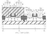
図52を参照して、次に、写真製版法によって、PMOSトランジスタの形成予定領域を覆ってフォトレジスト241を形成する。次に、フォトレジスト241を注入マスクに用いて、イオン注入法によって、n型の不純物をシリコン層31の上面内に注入することにより、不純物導入領域701を形成する。
Referring to FIG. 52, then, by photolithography, a
図53を参照して、次に、フォトレジスト241を除去する。次に、写真製版法によって、NMOSトランジスタの形成予定領域を覆ってフォトレジスト251を形成する。次に、フォトレジスト251を注入マスクに用いて、イオン注入法によって、p型の不純物をシリコン層32の上面内に注入することにより、不純物導入領域702を形成する。
Referring to FIG. 53, then, the photoresist is removed 24 1. Next, by photolithography, a
図54を参照して、次に、フォトレジスト251を除去する。次に、シリコン及びポリシリコンはエッチングされやすく、シリコン酸化膜及びシリコン窒化膜はエッチングされにくい条件で、異方性ドライエッチングを行う。これにより、ゲート絶縁膜61,62及び素子分離絶縁膜5,23から露出している部分のシリコン層31,32がエッチングされて、凹部141,142が形成される。また、ポリシリコン膜191,192の上部が併せてエッチングされて、ゲート電極71,72が形成される。
Referring to FIG. 54, then, the photoresist is removed 25 1. Next, anisotropic dry etching is performed under the condition that silicon and polysilicon are easily etched and the silicon oxide film and the silicon nitride film are hardly etched. As a result, portions of the silicon layers 3 1 and 3 2 exposed from the
図55を参照して、次に、写真製版法によって、PMOSトランジスタの形成予定領域を覆ってフォトレジスト242を形成する。次に、フォトレジスト242を注入マスクに用いて、イオン注入法によって、n型の不純物をシリコン層31の上面内に注入することにより、不純物導入領域111を形成する。
Referring to FIG. 55, then, by photolithography, a
図56を参照して、次に、フォトレジスト242を除去する。次に、写真製版法によって、NMOSトランジスタの形成予定領域を覆ってフォトレジスト252を形成する。次に、フォトレジスト252を注入マスクに用いて、イオン注入法によって、p型の不純物をシリコン層32の上面内に注入することにより、不純物導入領域112を形成する。
Referring to FIG. 56, then, the photoresist is removed 24 2. Next, by photolithography, a
その後、フォトレジスト252を除去した後、ゲート電極71,72及びソース・ドレイン領域121,122の各上面をシリサイド化することにより、半導体装置が完成する。
Then, after removing the
本実施の形態11に係る半導体装置の第1の製造方法によると、図45〜51に示した工程内では写真製版工程がトータル2回で足りる。そのため、図52〜56に示した工程内で写真製版工程がトータル4回必要である上記第2の製造方法と比較して、製造工程数を削減できるという効果が得られる。 According to the first manufacturing method of the semiconductor device according to the eleventh embodiment, the photolithography process in the processes shown in FIGS. Therefore, an effect is obtained that the number of manufacturing steps can be reduced as compared with the above-described second manufacturing method, which requires a total of four photolithography steps in the steps shown in FIGS.
一方、本実施の形態11に係る半導体装置の第2の製造方法によると、図54に示した1回のエッチング工程によって、凹部141,142が併せて形成される。そのため、凹部141,142が別個のエッチング工程によって形成される上記第1の製造方法と比較すると、エッチングに伴ってエッチングチャンバ内に発生するゴミを低減できる。その結果、歩留まりを向上できるという効果が得られる。また、エッチング及びイオン注入の双方の影響を受けるフォトレジスト24,25と比較すると、イオン注入の影響のみを受けるフォトレジスト242,252はアッシングによって除去しやすいという効果も得られる。
On the other hand, in the second method of manufacturing a semiconductor device according to
実施の形態12.
図57は、本発明の実施の形態12に係る半導体装置の製造方法の一工程を示す断面図である。まず、上記実施の形態1と同様の方法により、図6に示した構造を得る。
FIG. 57 is a cross-sectional view showing a step of a method of manufacturing a semiconductor device according to
次に、イオン注入法によって、凹部14の形成予定領域におけるシリコン層3内に、シリコンイオン80を注入する。注入濃度は、1015/cm2程度のオーダーである。但し、シリコンイオン80の代わりに、アルゴンイオン又はゲルマニウムイオン等を注入してもよい。これにより、凹部14の形成予定領域におけるシリコン層3がアモルファス化されて、アモルファスシリコン領域81が形成される。イオン注入法によってアモルファスシリコン領域81が形成されるため、シリコン層3の上面からアモルファスシリコン領域81の底面までの深さは、ウェハ面内において均一となる。その後は、図7に示した工程以降の工程が順に実行される。
Next,
このように本実施の形態12に係る半導体装置の製造方法によると、凹部14の形成予定領域におけるシリコン層3をアモルファス化した後に、アモルファスシリコン領域81をエッチングすることによって、凹部14が形成される。アモルファスシリコン領域81は、シリコン層3の他の部分(即ち単結晶シリコン領域)に比べてエッチングレートが十分に高い。従って、アモルファスシリコン領域81と単結晶シリコン領域とのエッチングレートの差に起因して、ウェハ面内において凹部14の深さを均一にすることができる。
As described above, according to the method of manufacturing a semiconductor device according to the twelfth embodiment, the
以上では、本実施の形態12に係る発明を上記実施の形態1に適用した例について述べたが、本実施の形態12に係る発明は、他の全ての実施の形態にも適用することが可能である。 In the above, the example in which the invention according to the twelfth embodiment is applied to the first embodiment has been described. However, the invention according to the twelfth embodiment can be applied to all the other embodiments. It is.
1 シリコン基板、2 BOX層、3 シリコン層、4 SOI基板、5 素子分離絶縁膜、6 ゲート絶縁膜、7 ゲート電極、8,13,43,52,53 コバルトシリサイド層、9,41,42 サイドウォール、10,11,70 不純物導入領域、12 ソース・ドレイン領域、14,21,22 凹部、15,17,18,20 シリコン酸化膜、16,19 ポリシリコン膜、40,60,62 シリコン窒化膜、50,51 シリコン層。
Claims (11)
前記半導体層の主面内に部分的に形成され、前記絶縁層とによって前記半導体層の一部を挟む底面を有する素子分離絶縁膜と、
前記素子分離絶縁膜によって規定される素子形成領域内において、前記半導体層の前記主面上に部分的に形成されたゲート構造と、
前記素子形成領域内において、前記ゲート構造から露出している部分の前記半導体層の前記主面内に形成され、前記ゲート構造の下方のチャネル形成領域を挟んで対を成す凹部と、
前記凹部の底面内に形成され、前記チャネル形成領域を挟んで対を成し、その底面又はその空乏層が前記絶縁層に到達し、前記第1導電型とは異なる第2導電型のソース・ドレイン領域と
を備える、半導体装置。 An SOI substrate having a structure in which a semiconductor substrate, an insulating layer, and a semiconductor layer of the first conductivity type are stacked in this order;
An element isolation insulating film partially formed in the main surface of the semiconductor layer and having a bottom surface sandwiching a part of the semiconductor layer with the insulating layer;
A gate structure partially formed on the main surface of the semiconductor layer in an element forming region defined by the element isolation insulating film;
A recess formed in the main surface of the portion of the semiconductor layer exposed from the gate structure in the element formation region and forming a pair with a channel formation region below the gate structure interposed therebetween;
A source / source of a second conductivity type different from the first conductivity type is formed in the bottom surface of the concave portion and forms a pair with the channel formation region interposed therebetween, and the bottom surface or a depletion layer thereof reaches the insulating layer. A semiconductor device comprising: a drain region.
前記半導体層の前記主面内に形成された、比較的低濃度の第1の不純物導入領域と、
前記第1の不純物導入領域よりも深く形成された、比較的高濃度の第2の不純物導入領域と
を有し、
前記半導体層の前記主面から前記凹部の前記底面までの深さは、前記半導体層の前記主面から前記第1の不純物導入領域の底面までの深さよりも浅い、請求項1〜3のいずれか一つに記載の半導体装置。 The source / drain region is
A first impurity introduction region having a relatively low concentration formed in the main surface of the semiconductor layer;
A second impurity introduction region having a relatively high concentration formed deeper than the first impurity introduction region;
The depth from the main surface of the semiconductor layer to the bottom surface of the recess is smaller than the depth from the main surface of the semiconductor layer to the bottom surface of the first impurity introduction region. The semiconductor device according to any one of the above.
前記半導体層の前記主面内に形成された、比較的低濃度の第1の不純物導入領域と、
前記第1の不純物導入領域よりも深く形成された、比較的高濃度の第2の不純物導入領域と、
前記半導体層の前記主面内に形成された第3の不純物導入領域と
を有し、
前記半導体層の前記主面から前記第3の不純物導入領域の底面までの深さは、前記半導体層の前記主面から前記第1の不純物導入領域の底面までの深さよりも深く、
前記半導体層の前記主面から前記凹部の前記底面までの深さは、前記半導体層の前記主面から前記第3の不純物導入領域の前記底面までの深さよりも浅い、請求項1〜3のいずれか一つに記載の半導体装置。 The source / drain region is
A first impurity introduction region having a relatively low concentration formed in the main surface of the semiconductor layer;
A second impurity introduction region having a relatively high concentration formed deeper than the first impurity introduction region;
A third impurity-introduced region formed in the main surface of the semiconductor layer;
A depth from the main surface of the semiconductor layer to a bottom surface of the third impurity-doped region is deeper than a depth from the main surface of the semiconductor layer to a bottom surface of the first impurity-doped region;
The depth from the main surface of the semiconductor layer to the bottom surface of the recess is smaller than the depth from the main surface of the semiconductor layer to the bottom surface of the third impurity introduction region. The semiconductor device according to any one of the above.
前記半導体層の前記主面上に形成されたゲート絶縁膜と、
前記ゲート絶縁膜上に形成されたゲート電極と、
前記ゲート電極の側面に形成された第1のサイドウォールと
を有し、
前記半導体装置は、
前記第1のサイドウォールに接して前記凹部の前記底面上に形成された第2のサイドウォールと、
前記第2のサイドウォールから露出している部分の前記ソース・ドレイン領域上に形成された、金属−半導体化合物層と
をさらに備える、請求項1〜6のいずれか一つに記載の半導体装置。 The gate structure comprises:
A gate insulating film formed on the main surface of the semiconductor layer,
A gate electrode formed on the gate insulating film;
A first sidewall formed on a side surface of the gate electrode,
The semiconductor device includes:
A second sidewall formed on the bottom surface of the recess in contact with the first sidewall;
The semiconductor device according to claim 1, further comprising a metal-semiconductor compound layer formed on a portion of the source / drain region exposed from the second sidewall.
前記金属−半導体化合物層は、前記第2及び第3のサイドウォールから露出している部分の前記ソース・ドレイン領域上に形成されている、請求項7に記載の半導体装置。 A third sidewall formed on the bottom surface of the concave portion in contact with the element isolation insulating film;
The semiconductor device according to claim 7, wherein the metal-semiconductor compound layer is formed on portions of the source / drain regions exposed from the second and third sidewalls.
前記半導体領域上に形成された金属−半導体化合物層と
をさらに備える、請求項1〜6のいずれか一つに記載の半導体装置。 A semiconductor region formed on the bottom surface of the recess,
The semiconductor device according to claim 1, further comprising a metal-semiconductor compound layer formed on the semiconductor region.
前記半導体装置は、前記NMOSトランジスタ及び前記PMOSトランジスタのうちのいずれか一方である、請求項1〜9のいずれか一つに記載の半導体装置。 An NMOS transistor and a PMOS transistor are formed in the SOI substrate,
The semiconductor device according to claim 1, wherein the semiconductor device is one of the NMOS transistor and the PMOS transistor.
前記半導体装置は、前記第1及び第2のトランジスタのうちのいずれか一方である、請求項1〜9のいずれか一つに記載の半導体装置。
In the SOI substrate, a first transistor that operates at a relatively low power supply voltage and a second transistor that operates at a relatively high power supply voltage are formed.
The semiconductor device according to claim 1, wherein the semiconductor device is one of the first and second transistors.
Priority Applications (6)
| Application Number | Priority Date | Filing Date | Title |
|---|---|---|---|
| JP2003295234A JP2004241755A (en) | 2003-01-15 | 2003-08-19 | Semiconductor device |
| KR10-2004-0000165A KR100523310B1 (en) | 2003-01-15 | 2004-01-03 | Semiconductor device |
| US10/754,539 US7067881B2 (en) | 2003-01-15 | 2004-01-12 | Semiconductor device |
| TW093100764A TWI231044B (en) | 2003-01-15 | 2004-01-13 | Semiconductor device |
| CNB2004100018675A CN100336228C (en) | 2003-01-15 | 2004-01-15 | Semiconductor device |
| US11/197,397 US20050275021A1 (en) | 2003-01-15 | 2005-08-05 | Semiconductor device |
Applications Claiming Priority (2)
| Application Number | Priority Date | Filing Date | Title |
|---|---|---|---|
| JP2003006641 | 2003-01-15 | ||
| JP2003295234A JP2004241755A (en) | 2003-01-15 | 2003-08-19 | Semiconductor device |
Publications (2)
| Publication Number | Publication Date |
|---|---|
| JP2004241755A true JP2004241755A (en) | 2004-08-26 |
| JP2004241755A5 JP2004241755A5 (en) | 2006-09-28 |
Family
ID=32964739
Family Applications (1)
| Application Number | Title | Priority Date | Filing Date |
|---|---|---|---|
| JP2003295234A Pending JP2004241755A (en) | 2003-01-15 | 2003-08-19 | Semiconductor device |
Country Status (5)
| Country | Link |
|---|---|
| US (2) | US7067881B2 (en) |
| JP (1) | JP2004241755A (en) |
| KR (1) | KR100523310B1 (en) |
| CN (1) | CN100336228C (en) |
| TW (1) | TWI231044B (en) |
Cited By (8)
| Publication number | Priority date | Publication date | Assignee | Title |
|---|---|---|---|---|
| JP2006310772A (en) * | 2005-03-28 | 2006-11-09 | Toshiba Corp | Fin-type channel transistor and method for manufacturing thereof |
| JP2007042964A (en) * | 2005-08-05 | 2007-02-15 | Matsushita Electric Ind Co Ltd | Semiconductor device and method of manufacturing same |
| JP2007173356A (en) * | 2005-12-20 | 2007-07-05 | Renesas Technology Corp | Semiconductor device and its manufacturing method |
| JP2007201240A (en) * | 2006-01-27 | 2007-08-09 | Renesas Technology Corp | Semiconductor device and its manufacturing method |
| JP2008515205A (en) * | 2004-09-29 | 2008-05-08 | インターナショナル・ビジネス・マシーンズ・コーポレーション | Structure and method for fabricating strained channel field effect transistors using sacrificial spacers |
| CN102208448A (en) * | 2011-05-24 | 2011-10-05 | 西安电子科技大学 | Polycrystalline Si1-xGex/metal parallel covering double-gate strained SiGe-on-insulator (SSGOI) n metal oxide semiconductor field effect transistor (MOSFET) device structure |
| JP2015073137A (en) * | 2006-12-05 | 2015-04-16 | 株式会社半導体エネルギー研究所 | Semiconductor device and semiconductor device manufacturing method |
| JP2015073138A (en) * | 2006-12-05 | 2015-04-16 | 株式会社半導体エネルギー研究所 | Semiconductor device and semiconductor device manufacturing method |
Families Citing this family (39)
| Publication number | Priority date | Publication date | Assignee | Title |
|---|---|---|---|---|
| KR100543472B1 (en) | 2004-02-11 | 2006-01-20 | 삼성전자주식회사 | Semiconductor device having depletion barrier layer at source/drain regions and method of forming the same |
| US8669145B2 (en) * | 2004-06-30 | 2014-03-11 | International Business Machines Corporation | Method and structure for strained FinFET devices |
| JP4175650B2 (en) * | 2004-08-26 | 2008-11-05 | シャープ株式会社 | Manufacturing method of semiconductor device |
| JP4440080B2 (en) * | 2004-11-12 | 2010-03-24 | 株式会社東芝 | Semiconductor device and manufacturing method thereof |
| JP4081071B2 (en) * | 2004-11-26 | 2008-04-23 | 株式会社東芝 | Semiconductor memory device and manufacturing method thereof |
| US7465972B2 (en) | 2005-01-21 | 2008-12-16 | Taiwan Semiconductor Manufacturing Company, Ltd. | High performance CMOS device design |
| KR100632460B1 (en) * | 2005-02-03 | 2006-10-11 | 삼성전자주식회사 | Method for fabricating semiconductor device |
| JP4718894B2 (en) * | 2005-05-19 | 2011-07-06 | 株式会社東芝 | Manufacturing method of semiconductor device |
| US7118954B1 (en) * | 2005-05-26 | 2006-10-10 | United Microelectronics Corp. | High voltage metal-oxide-semiconductor transistor devices and method of making the same |
| JP2007005575A (en) * | 2005-06-24 | 2007-01-11 | Renesas Technology Corp | Semiconductor device and its manufacturing method |
| JP4822791B2 (en) * | 2005-10-04 | 2011-11-24 | ルネサスエレクトロニクス株式会社 | Semiconductor memory device |
| TW200733244A (en) * | 2005-10-06 | 2007-09-01 | Nxp Bv | Semiconductor device |
| US7659172B2 (en) * | 2005-11-18 | 2010-02-09 | International Business Machines Corporation | Structure and method for reducing miller capacitance in field effect transistors |
| US20070212861A1 (en) * | 2006-03-07 | 2007-09-13 | International Business Machines Corporation | Laser surface annealing of antimony doped amorphized semiconductor region |
| US7820519B2 (en) | 2006-11-03 | 2010-10-26 | Freescale Semiconductor, Inc. | Process of forming an electronic device including a conductive structure extending through a buried insulating layer |
| US8188543B2 (en) * | 2006-11-03 | 2012-05-29 | Freescale Semiconductor, Inc. | Electronic device including a conductive structure extending through a buried insulating layer |
| US7572706B2 (en) * | 2007-02-28 | 2009-08-11 | Freescale Semiconductor, Inc. | Source/drain stressor and method therefor |
| DE102007030053B4 (en) * | 2007-06-29 | 2011-07-21 | Advanced Micro Devices, Inc., Calif. | Reduce pn junction capacitance in a transistor by lowering drain and source regions |
| GB0717976D0 (en) * | 2007-09-14 | 2007-10-31 | Tavkhelldze Avto | Quantum interference depression effect MOS transistor |
| US7687862B2 (en) * | 2008-05-13 | 2010-03-30 | Infineon Technologies Ag | Semiconductor devices with active regions of different heights |
| CN101728263B (en) * | 2008-10-24 | 2011-07-06 | 中芯国际集成电路制造(上海)有限公司 | Method for controlling source/drain junction capacitance and method for forming PMOS transistor |
| WO2010049086A2 (en) * | 2008-10-31 | 2010-05-06 | Advanced Micro Devices, Inc. | Recessed drain and source areas in combination with advanced silicide formation in transistors |
| DE102008054075B4 (en) * | 2008-10-31 | 2010-09-23 | Advanced Micro Devices, Inc., Sunnyvale | Semiconductor device having a lowered drain and source region in conjunction with a method of complex silicide fabrication in transistors |
| US7759142B1 (en) * | 2008-12-31 | 2010-07-20 | Intel Corporation | Quantum well MOSFET channels having uni-axial strain caused by metal source/drains, and conformal regrowth source/drains |
| US8105887B2 (en) * | 2009-07-09 | 2012-01-31 | International Business Machines Corporation | Inducing stress in CMOS device |
| US9209098B2 (en) * | 2011-05-19 | 2015-12-08 | Taiwan Semiconductor Manufacturing Company, Ltd. | HVMOS reliability evaluation using bulk resistances as indices |
| US8748285B2 (en) | 2011-11-28 | 2014-06-10 | International Business Machines Corporation | Noble gas implantation region in top silicon layer of semiconductor-on-insulator substrate |
| US8603868B2 (en) * | 2011-12-19 | 2013-12-10 | International Business Machines Corporation | V-groove source/drain MOSFET and process for fabricating same |
| JP6083930B2 (en) * | 2012-01-18 | 2017-02-22 | キヤノン株式会社 | Photoelectric conversion device, imaging system, and method of manufacturing photoelectric conversion device |
| US8872228B2 (en) * | 2012-05-11 | 2014-10-28 | Taiwan Semiconductor Manufacturing Company, Ltd. | Strained-channel semiconductor device fabrication |
| JP5944266B2 (en) | 2012-08-10 | 2016-07-05 | ルネサスエレクトロニクス株式会社 | Semiconductor device and manufacturing method thereof |
| US9698024B2 (en) | 2012-12-06 | 2017-07-04 | Taiwan Semiconductor Manufacturing Co., Ltd. | Partial SOI on power device for breakdown voltage improvement |
| US9202916B2 (en) * | 2013-12-27 | 2015-12-01 | Taiwan Semiconductor Manufacturing Co., Ltd. | Semiconductor device structure |
| US9941388B2 (en) * | 2014-06-19 | 2018-04-10 | Globalfoundries Inc. | Method and structure for protecting gates during epitaxial growth |
| CN105762106B (en) * | 2014-12-18 | 2021-02-19 | 联华电子股份有限公司 | Semiconductor device and manufacturing process thereof |
| US10050147B2 (en) * | 2015-07-24 | 2018-08-14 | Taiwan Semiconductor Manufacturing Co., Ltd. | Semiconductor device and manufacturing method thereof |
| KR102619874B1 (en) | 2016-06-23 | 2024-01-03 | 삼성전자주식회사 | Semiconductor device having an impurity region |
| US9741850B1 (en) * | 2016-08-12 | 2017-08-22 | United Microelectronics Corp. | Semiconductor device and method for forming the same |
| US20230157007A1 (en) * | 2021-11-17 | 2023-05-18 | Nanya Technology Corporation | Memory array structure with contact enhancement sidewall spacers |
Family Cites Families (8)
| Publication number | Priority date | Publication date | Assignee | Title |
|---|---|---|---|---|
| US5710450A (en) * | 1994-12-23 | 1998-01-20 | Intel Corporation | Transistor with ultra shallow tip and method of fabrication |
| FR2749977B1 (en) * | 1996-06-14 | 1998-10-09 | Commissariat Energie Atomique | QUANTUM WELL MOS TRANSISTOR AND METHODS OF MANUFACTURE THEREOF |
| US5889331A (en) * | 1996-12-31 | 1999-03-30 | Intel Corporation | Silicide for achieving low sheet resistance on poly-Si and low Si consumption in source/drain |
| JP3070501B2 (en) | 1997-01-20 | 2000-07-31 | 日本電気株式会社 | Semiconductor device |
| US6777759B1 (en) | 1997-06-30 | 2004-08-17 | Intel Corporation | Device structure and method for reducing silicide encroachment |
| US6518155B1 (en) * | 1997-06-30 | 2003-02-11 | Intel Corporation | Device structure and method for reducing silicide encroachment |
| JP4823408B2 (en) * | 2000-06-08 | 2011-11-24 | ルネサスエレクトロニクス株式会社 | Nonvolatile semiconductor memory device |
| JP2002141420A (en) * | 2000-10-31 | 2002-05-17 | Mitsubishi Electric Corp | Semiconductor device and manufacturing method of it |
-
2003
- 2003-08-19 JP JP2003295234A patent/JP2004241755A/en active Pending
-
2004
- 2004-01-03 KR KR10-2004-0000165A patent/KR100523310B1/en not_active IP Right Cessation
- 2004-01-12 US US10/754,539 patent/US7067881B2/en not_active Expired - Fee Related
- 2004-01-13 TW TW093100764A patent/TWI231044B/en not_active IP Right Cessation
- 2004-01-15 CN CNB2004100018675A patent/CN100336228C/en not_active Expired - Fee Related
-
2005
- 2005-08-05 US US11/197,397 patent/US20050275021A1/en not_active Abandoned
Cited By (9)
| Publication number | Priority date | Publication date | Assignee | Title |
|---|---|---|---|---|
| JP2008515205A (en) * | 2004-09-29 | 2008-05-08 | インターナショナル・ビジネス・マシーンズ・コーポレーション | Structure and method for fabricating strained channel field effect transistors using sacrificial spacers |
| JP2006310772A (en) * | 2005-03-28 | 2006-11-09 | Toshiba Corp | Fin-type channel transistor and method for manufacturing thereof |
| JP2007042964A (en) * | 2005-08-05 | 2007-02-15 | Matsushita Electric Ind Co Ltd | Semiconductor device and method of manufacturing same |
| JP2007173356A (en) * | 2005-12-20 | 2007-07-05 | Renesas Technology Corp | Semiconductor device and its manufacturing method |
| JP2007201240A (en) * | 2006-01-27 | 2007-08-09 | Renesas Technology Corp | Semiconductor device and its manufacturing method |
| US8350331B2 (en) | 2006-01-27 | 2013-01-08 | Renesas Electronics Corporation | Semiconductor device and manufacturing method for the same |
| JP2015073137A (en) * | 2006-12-05 | 2015-04-16 | 株式会社半導体エネルギー研究所 | Semiconductor device and semiconductor device manufacturing method |
| JP2015073138A (en) * | 2006-12-05 | 2015-04-16 | 株式会社半導体エネルギー研究所 | Semiconductor device and semiconductor device manufacturing method |
| CN102208448A (en) * | 2011-05-24 | 2011-10-05 | 西安电子科技大学 | Polycrystalline Si1-xGex/metal parallel covering double-gate strained SiGe-on-insulator (SSGOI) n metal oxide semiconductor field effect transistor (MOSFET) device structure |
Also Published As
| Publication number | Publication date |
|---|---|
| CN1519946A (en) | 2004-08-11 |
| US20050275021A1 (en) | 2005-12-15 |
| KR100523310B1 (en) | 2005-10-24 |
| KR20040065998A (en) | 2004-07-23 |
| US20040227185A1 (en) | 2004-11-18 |
| US7067881B2 (en) | 2006-06-27 |
| TW200414547A (en) | 2004-08-01 |
| CN100336228C (en) | 2007-09-05 |
| TWI231044B (en) | 2005-04-11 |
Similar Documents
| Publication | Publication Date | Title |
|---|---|---|
| JP2004241755A (en) | Semiconductor device | |
| US10263078B2 (en) | Method of manufacturing a MISFET on an SOI substrate | |
| US20080064173A1 (en) | Semiconductor device, cmos device and fabricating methods of the same | |
| JP5153121B2 (en) | Field effect transistor device and method for forming the same | |
| JP2701762B2 (en) | Semiconductor device and manufacturing method thereof | |
| US20080090360A1 (en) | Methods for fabricating multiple finger transistors | |
| KR20030004144A (en) | Semiconductor device and method for manufacturing the same | |
| US7648880B2 (en) | Nitride-encapsulated FET (NNCFET) | |
| KR101326393B1 (en) | Semiconductor device | |
| JP2009158677A (en) | Method of manufacturing semiconductor device and method of manufacturing semiconductor device for hybrid transistor | |
| JP2002353449A (en) | Method of manufacturing semiconductor element | |
| US7723777B2 (en) | Semiconductor device and method for making same | |
| US7514747B2 (en) | Silicon-on-insulator semiconductor device | |
| JP2003060064A (en) | Mosfet, semiconductor device and its fabricating method | |
| JP6574885B2 (en) | Manufacturing method of semiconductor device | |
| TWI626678B (en) | High gain transistor for analog applications | |
| JP2006049365A (en) | Semiconductor device | |
| JP2005259945A (en) | Semiconductor device and manufacturing method thereof | |
| JP2018148244A (en) | Semiconductor device | |
| JP3038740B2 (en) | Method for manufacturing semiconductor device | |
| KR101231229B1 (en) | Method for manufacturing transistor in semiconductor device | |
| KR100943133B1 (en) | Transistor of semiconductor device and forming method thereof | |
| JP2004031529A (en) | Semiconductor device and its manufacturing method | |
| JP2005101064A (en) | Method for manufacturing semiconductor device | |
| KR20070001592A (en) | Method for forming gate of semiconductor device |
Legal Events
| Date | Code | Title | Description |
|---|---|---|---|
| A521 | Request for written amendment filed |
Free format text: JAPANESE INTERMEDIATE CODE: A523 Effective date: 20060811 |
|
| A621 | Written request for application examination |
Free format text: JAPANESE INTERMEDIATE CODE: A621 Effective date: 20060811 |
|
| A131 | Notification of reasons for refusal |
Free format text: JAPANESE INTERMEDIATE CODE: A131 Effective date: 20090707 |
|
| A977 | Report on retrieval |
Free format text: JAPANESE INTERMEDIATE CODE: A971007 Effective date: 20090709 |
|
| A02 | Decision of refusal |
Free format text: JAPANESE INTERMEDIATE CODE: A02 Effective date: 20091104 |