JP2004201440A - Method and apparatus for pulse width modulation, power conversion method, and power converter - Google Patents
Method and apparatus for pulse width modulation, power conversion method, and power converter Download PDFInfo
- Publication number
- JP2004201440A JP2004201440A JP2002368421A JP2002368421A JP2004201440A JP 2004201440 A JP2004201440 A JP 2004201440A JP 2002368421 A JP2002368421 A JP 2002368421A JP 2002368421 A JP2002368421 A JP 2002368421A JP 2004201440 A JP2004201440 A JP 2004201440A
- Authority
- JP
- Japan
- Prior art keywords
- voltage
- pulse width
- width modulation
- command signal
- voltage command
- Prior art date
- Legal status (The legal status is an assumption and is not a legal conclusion. Google has not performed a legal analysis and makes no representation as to the accuracy of the status listed.)
- Granted
Links
Images


Classifications
-
- H—ELECTRICITY
- H02—GENERATION; CONVERSION OR DISTRIBUTION OF ELECTRIC POWER
- H02M—APPARATUS FOR CONVERSION BETWEEN AC AND AC, BETWEEN AC AND DC, OR BETWEEN DC AND DC, AND FOR USE WITH MAINS OR SIMILAR POWER SUPPLY SYSTEMS; CONVERSION OF DC OR AC INPUT POWER INTO SURGE OUTPUT POWER; CONTROL OR REGULATION THEREOF
- H02M7/00—Conversion of ac power input into dc power output; Conversion of dc power input into ac power output
- H02M7/42—Conversion of dc power input into ac power output without possibility of reversal
- H02M7/44—Conversion of dc power input into ac power output without possibility of reversal by static converters
- H02M7/48—Conversion of dc power input into ac power output without possibility of reversal by static converters using discharge tubes with control electrode or semiconductor devices with control electrode
- H02M7/53—Conversion of dc power input into ac power output without possibility of reversal by static converters using discharge tubes with control electrode or semiconductor devices with control electrode using devices of a triode or transistor type requiring continuous application of a control signal
- H02M7/537—Conversion of dc power input into ac power output without possibility of reversal by static converters using discharge tubes with control electrode or semiconductor devices with control electrode using devices of a triode or transistor type requiring continuous application of a control signal using semiconductor devices only, e.g. single switched pulse inverters
- H02M7/5387—Conversion of dc power input into ac power output without possibility of reversal by static converters using discharge tubes with control electrode or semiconductor devices with control electrode using devices of a triode or transistor type requiring continuous application of a control signal using semiconductor devices only, e.g. single switched pulse inverters in a bridge configuration
- H02M7/53871—Conversion of dc power input into ac power output without possibility of reversal by static converters using discharge tubes with control electrode or semiconductor devices with control electrode using devices of a triode or transistor type requiring continuous application of a control signal using semiconductor devices only, e.g. single switched pulse inverters in a bridge configuration with automatic control of output voltage or current
Abstract
Description
【0001】
【発明の属する技術分野】
本発明は、電力変換器を制御するための新規なパルス幅変調方法とその装置及び電力変換方法と電力変換器に関する。
【0002】
【従来の技術】
【非特許文献1】Derivation of motor line-current waveforms from the DC-link current of an inverter"IEE PROCEEDING、 Vol.136、Pt. B、 JULY 1989、pp.196-204
【特許文献1】特開2001-327173号公報
【特許文献2】特開2002-119062号公報
【特許文献3】特開2002- 95263号公報
【0003】
直流をパルス幅変調により交流に変換する電力変換器において、直流側の電流から交流側の電流を検出する方法として、非特許文献1に記載の方法がある。また、この電流検出方法に適したパルス幅変調方式としては、特許文献1及び特許文献2に記載の方法がある。PWM制御部及び電流検出部の詳細は例えば、特許文献3に記載されている。
【0004】
【発明が解決しようとする課題】
非特許文献1においては、交流電圧が低い場合、直流側の電流パルス幅が小さくなるため、直流側の電流を安定して検出することが難しい。これに対し、特許文献1では、パルス幅変調の搬送波の一周期前半では、直流側の電流パルス幅が電流を安定に検出するのに十分な幅となるように補正し、後半で交流側電圧が所望の電圧となるように補正を行う。このため、後半では電流検出に必要なパルス幅が確保されないこと、及び搬送波の周期の2分の1の周期で変調波を演算する必要があり、演算には高性能なマイクロコンピュータが必要となる。また、特許文献1においても、電流を検出するのに必要な電流パルス幅が確保できない場合がある。
【0005】
更に、特許文献1及び特許文献2に記載の方法では、ある相のスイッチングと他の相のスイッチングが短時間で行われる場合が存在し、このときに発生する相互干渉により正常なスイッチングができない現象を防止することはできない。
【0006】
以上のように、従来の直流を交流に変換するパルス幅変調を用いた電力変換器において、直流電流Idcから電力変換器の出力電流を検出する場合、相間の電圧指令信号が小さい場合、直流電流Idcのパルス幅が狭くなり、検出が困難である。
【0007】
本発明の目的は、直流側の電流パルス幅を電流検出が可能な幅以上にすることができ、スイッチングの相互干渉が発生しないパルス幅変調方法とその装置及び電力変換方法と電力変換器を提供することにある。
【0008】
【課題を解決するための手段】
本発明は、3つの第1指令信号における各々3つの指令信号差の中の任意の2つ又は3つの前記指令信号の差をいずれも予め定められた値以上になるように第2指令信号を演算するステップと、該第2指令信号に基づきパルス幅変調するステップとを有することを特徴とするパルス幅変調方法にある。
【0009】
本発明は、より具体的には、3つの第1指令信号に基づき演算された3つの第2指令信号をパルス幅変調するパルス幅変調方法において、任意の2つの第2指令信号の差をいずれも予め定められた値以上及び前記3つの第1指令信号と前記3つの第2指令信号とのそれぞれの差の積算値である3つの誤差積算値がいずれも予め定められた値以下となるように前記第1指令信号に基づき前記第2指令信号を演算するステップと、前記第2指令信号をパルス幅変調するステップとを有すること、又、3つの第1指令信号と該3つの第1指令信号に基づき補正された3つの第2指令信号との差の積算値である3つの誤差積算値を前記3つの第1指令信号にそれぞれ加算し3つの第3指令信号を演算するステップと、任意の2つの前記第3指令信号差を予め定められた値以上になるように前記第2指令信号を演算するステップとを有することを特徴とする。
【0010】
本発明は、電力変換方法として、第1交流電圧指令信号に基づき第2交流電圧指令信号を演算する電圧指令信号補正ステップと、前記第2交流電圧指令信号に基づきパルス幅変調を行いゲート信号を出力するPWM制御ステップと、前記ゲート信号に基づき直流電圧をスイチングし交流電圧に変換するステップとを有し,前記パルス幅変調は前述に記載のパルス幅変調方法よりなることを特徴とし、又外部から与えられる速度指令信号に基づき前記第1交流電圧指令信号を出力するモータ制御ステップを有することを特徴とする。
【0011】
本発明は、3つの指令信号における任意の2つの前記指令信号の差が予め定められた値以上になるように演算する補正手段と、該演算された出力をパルス幅変調するパルス幅変調手段とを有することを特徴とするパルス幅変調装置にある。
【0012】
又、本発明は、3つの第1指令信号に基づき演算された3つの第2指令信号をパルス幅変調するパルス幅変調手段を有するパルス幅変調装置において、前記第2指令信号の任意の2つの指令信号の差を予め定められた値以上及び前記3つの第1指令信号と前記3つの第2指令信号とのそれぞれの差の積算値が予め定められた値以下となるように前記第2指令信号を演算する補正手段を有すること、又、3つの第1指令信号と該3つの第1指令信号に基づき補正された3つの第2指令信号との差の積算値である3つの誤差積算値を前記3つの第1指令信号にそれぞれ加算し3つの第3指令信号を演算する演算手段と、任意の2つの第3指令信号差を予め定められた値以上になるように前記第2指令信号を補正する補正手段とを有することを特徴とする。
【0013】
本発明は、第1交流電圧指令信号に基づき第2交流電圧指令信号を演算する電圧指令補正部と、前記第2の交流電圧指令信号に基づきパルス幅変調を行いゲート信号を出力するPWM制御部と、前記ゲート信号に基づき直流電圧をスイチングし交流電圧に変換するスイッチング素子とを有する直流電圧を交流電圧に変換する電力変換器において,前記パルス幅変調を前述に記載のパルス幅変調装置により行うことを特徴とする。
【0014】
即ち、本発明により、3つの入力信号の各々の差の中の任意の2つの変調波の差を最低値以上にすることができるため、パルス幅変調した結果であるパルス出力において、任意の2つのパルスが変化する間隔を前記最低値に相当する時間以上にできる。また、このパルス幅変調方式を電力変換器に適用することにより、直流電流のパルス幅も前記最低値に相当する時間以上となるため、直流電流の検出が可能になり、直流側の電流パルス幅を必ず電流検出が可能な幅以上にすることができる。また、パルスが変化する間隔が確保されるため、スイッチングの相互干渉を抑制することができる。
【0015】
又、3つの信号とそれぞれの誤差積算値を加算し、加算結果の任意の2つの指令信号の差が最低値以上になるように補正し、補正結果に基づきパルス幅変調すると共に、補正結果と前記加算手段の加算結果の差から誤差積算値を更新するパルス幅変調方法が好ましい。
【0016】
また、直流電流のパルス幅が必ず確保されることから、補正結果の更新を搬送波の半周期毎又はその整数倍にしても、電流検出に支障は来さないため、演算周期を大きくすることができ、パルス幅変調方法の単位時間あたりの演算量を低減することができる。前記指令信号は電圧指令信号であり、前記補正により生じる誤差を前記電圧指令信号に加算することが好ましい。
【0017】
【発明の実施の形態】
(実施例1)
図1は、本発明のパルス幅変調方法を用いた電力変換器の一例を示す構成図である。図1において、整流回路2、平滑コンデンサ3、電流検出器5、電流検出部7、外部から与えられる速度指令に基づき前記第1の交流電圧指令信号を出力するモータ制御部8、前記第1交流電圧指令信号に基づき第2交流電圧指令信号に補正する電圧指令補正部9、前記第2の交流電圧指令信号に基づきパルス幅変調を行いゲート信号を出力するPWM制御部6、前記ゲート信号に基づき直流電圧をスイチングし交流電圧に変換するスイッチング素子Qu、Qv、Qw、Qx、Qy及びQz、を有する直流電圧を交流電圧に変換する電力変換器10と、交流電源1と、モータ4とを備えたものである。
【0018】
交流電源1から供給される電圧を整流回路2で整流し、さらに平滑コンデンサ3で平滑し、直流電圧に変換する。変換された直流電圧をスイッチング素子Qu、Qv、Qw、Qx、Qy、及びQzをスイッチングすることにより、モータ4に接続されたU相、V相及びW相の電圧を制御する。
【0019】
電流検出器5は、スイッチング素子Qx、Qy、及びQzから平滑コンデンサ3に流れる直流電流Idcを検出し、電流検出部7では検出した直流電流IdcとPWM制御部6が出力するゲート信号Gu、Gv、Gw、Gx、Gy、及びGzからモータ4に流れるU相モータ電流Iu、V相モータ電流Iv、及びW相モータ電流Iwを検出する。検出したモータ電流Iu、Iv、及びIwと外部から与えられる速度指令Fr*に基づき、モータ制御部8は第1のU相交流電圧指令信号Eu、第1のV相交流電圧指令信号Ev、及び第1のW相交流電圧指令信号Ewを出力する。
【0020】
電圧指令補正部9では、第1の交流電圧指令信号Eu、Ev、及びEwを補正することにより、第2のU相交流電圧指令信号Eu'、第2のV相交流電圧指令信号Ev'及び第2のW相交流電圧指令信号Ew'を出力し、PWM制御部6は第2の交流電圧指令信号Eu'、Ev'、及びEw'に基づきパルス幅変調を行い、スイッチング素子Qu、Qv、Qw、Qx、Qy、及びQzのスイッチングをそれぞれ指令するゲート信号Gu、Gv、Gw、Gx、Gy、及びGzを出力する。
【0021】
尚,本実施例では,交流電源1から整流回路2及び平滑コンデンサ3から直流電圧を生成しているが,これを直流電源に置き換えた場合には整流回路2及び平滑コンデンサ3は不要である。
【0022】
電圧指令補正部9では,第2の交流電圧指令信号Eu'、Ev'、及びEw'のうちの任意の2つの交流電圧指令信号の差が予め定められた値以上になるようするとともに,第1の交流電圧指令信号Eu、Ev、及びEwと第2の交流電圧指令信号Eu'、Ev'、及びEw'とのそれぞれの差を積算した誤差積算値dEu,dEv,及びdEwの絶対値がある値以上にならないように第2の交流電圧指令信号Eu'、Ev'、及びEw'を演算する。
【0023】
具体的には,電圧指令補正部9では,第1の交流電圧指令信号Eu、Ev、及びEwと第2の交流電圧指令信号Eu'、Ev'、及びEw'とのそれぞれの差を積算した誤差積算値dEu,dEv,及びdEwを求め,誤差積算値dEu,dEv,及びdEwと第1の交流電圧指令信号Eu、Ev、及びEwをそれぞれ加算した値に基づき,第2の交流電圧指令信号Eu'、Ev'、及びEw'のうちの任意の2つの交流電圧指令信号の差が予め定められた値以上になるよう処理を行う。
【0024】
電圧指令補正部9について,図2〜図5を用いてさらに詳細に説明する。図2は、電圧指令補正部9が出力である第2の交流電圧指令信号Eu'、Ev'、及びEw'を更新するタイミングを示す図である。図2において、201はPWM制御部6のパルス幅変調で用いる搬送波、202〜208は電圧指令補正部9が出力を更新するタイミングである。電圧指令補正部9は搬送波201の半周期毎に後述する処理を行い、第2の交流電圧指令信号Eu'、Ev'、及びEw'を出力する。図3、4に示す処理がメインの処理であり、図5に示す処理はサブルーチンである。
【0025】
図3は、電圧指令補正部のメインの処理を行う流れを示す図である。電圧指令補正部9では最初に、処理300を実行する。処理300では、U相交流電圧指令信号EuとU相誤差積算値dEuの加算結果を第3のU相交流電圧指令信号Eu0に、V相交流電圧指令信号EvとV相誤差積算値dEvの加算結果を第3のV相交流電圧指令信号Ev0に、U相交流電圧指令信号EuとU相誤差積算値dEuの加算結果を第3のW相交流電圧指令信号Ev0に、それぞれ代入して、次に処理301を実行する。
【0026】
処理301では、第3のU相交流電圧指令信号Eu0と第3のV相交流電圧指令信号Ev0を比較し、Eu0がEv0以上である場合は、処理302を実行し、Eu0がEv0未満である場合は、次に図4の処理401を実行する。
【0027】
処理302では、第3のV相交流電圧指令信号Ev0と第3のW相交流電圧指令信号Ew0を比較し、Ev0がEw0以上である場合は、処理303を実行し、Ev0がEw0未満である場合は、処理306を実行する。
【0028】
処理303では、第3のU相交流電圧指令信号Eu0を第1の最大電圧Eaに、第3のV相交流電圧指令信号Ev0を第1の中間電圧Ebに、第3のW相交流電圧指令信号Ew0を第1の最小電圧Ecに、それぞれ代入して、処理304を実行する。処理304の補正処理の詳細は後述する。
【0029】
処理304の後、処理305を実行し、第2の最大電圧Ea'を第2のU相交流電圧指令信号Eu'に、第2の中間電圧Eb'を第2のV相交流電圧指令信号Ev'に、第2の最小電圧Ec'を第2のW相交流電圧指令信号Ew'に、それぞれ代入して、次に処理313を実行する。
【0030】
処理313では、第3のU相交流電圧指令信号Eu0から第2のU相交流電圧指令信号Eu'を減算した値で、U相誤差積算値dEuを、第3のV相交流電圧指令信号Ev0から第2のV相交流電圧指令信号Ev'を減算した値で、V相誤差積算値dEvを、第3のW相交流電圧指令信号Ew0から第2のW相交流電圧指令信号Ew'を減算した値で、W相誤差積算値dEwを、それぞれ更新し、電圧指令補正部9の処理を終了する。
【0031】
又、処理302の後、処理306を実行する場合、処理306では、第3のU相交流電圧指令信号Eu0と第3のW相交流電圧指令信号Ew0を比較し、Eu0がEw0以上である場合は、次に処理307を実行し、Eu0がEw0未満である場合は、処理310を実行する。
【0032】
処理306の後、処理307を実行する場合、処理307では、第3のU相交流電圧指令信号Eu0を第1の最大電圧Eaに、第3のW相交流電圧指令信号Ew0を第1の中間電圧Ebに、第3のV相交流電圧指令信号Ev0を第1の最小電圧Ecに、それぞれ代入して、処理308を実行する。処理308の補正処理の詳細は後述する。
【0033】
処理308の後、処理309を実行し、第2の最大電圧Ea'を第2のU相交流電圧指令信号Eu'に、第2の中間電圧Eb'を第2のW相交流電圧指令信号Ew'に、第2の最小電圧Ec'を第2のV相交流電圧指令信号Ev'に、それぞれ代入して、処理313を実行し、電圧指令補正部9の処理を終了する。
【0034】
処理306の後、処理310を実行する場合、処理310では、第3のW相交流電圧指令信号Ew0を第1の最大電圧Eaに、第3のU相交流電圧指令信号Eu0を第1の中間電圧Ebに、第3のV相交流電圧指令信号Ev0を第1の最小電圧Ecに、それぞれ代入して、処理311を実行する。処理311の補正処理の詳細は後述する。
【0035】
処理311の後、処理312を実行し、第2の最大電圧Ea'を第2のW相交流電圧指令信号Ew'に、第2の中間電圧Eb'を第2のU相交流電圧指令信号Eu'に、第2の最小電圧Ec'を第2のV相交流電圧指令信号Ev'に、それぞれ代入して、処理313を実行し、電圧指令補正部9の処理を終了する。
【0036】
図4は、図3の電圧指令補正部9のメインの処理を行う流れの他の部分を示す図である。図4に処理301においてEu0がEv0未満である場合は、処理401を実行する。処理401では、第3のU相交流電圧指令信号Ew0と第3のW相交流電圧指令信号Ew0を比較し、Eu0がEw0以上である場合は、次に処理402を実行し、Eu0がEw0未満である場合は、処理405を実行する。
【0037】
処理402では、第3のV相交流電圧指令信号Ev0を第1の最大電圧Eaに、第3のU相交流電圧指令信号Eu0を第1の中間電圧Ebに、第3のW相交流電圧指令信号Ew0を第1の最小電圧Ecに、それぞれ代入して、処理403を実行する。
【0038】
処理403の後、処理404を実行し、第2の最大電圧Ea'を第2のV相交流電圧指令信号Ev'に、第2の中間電圧Eb'を第2のU相交流電圧指令信号Eu'に、第2の最小電圧Ec'を第2のW相交流電圧指令信号Ew'に、それぞれ代入して、処理313を実行して、電圧指令補正部9の処理を終了する。
【0039】
処理405では、第3のU相交流電圧指令信号Eu0と第3のW相交流電圧指令信号Ew0を比較し、Eu0がEw0以上である場合は、処理406を実行し、Eu0がEw0未満である場合は、次に処理409を実行する。
【0040】
処理406では、第3のV相交流電圧指令信号Ev0を第1の最大電圧Eaに、第3のW相交流電圧指令信号Ew0を第1の中間電圧Ebに、第3のU相交流電圧指令信号Eu0を第1の最小電圧Ecに、それぞれ代入して、処理407を実行する。
【0041】
処理407の後、処理408を実行し、第2の最大電圧Ea'を第2のV相交流電圧指令信号Ev'に、第2の中間電圧Eb'を第2のW相交流電圧指令信号Ew'に、第2の最小電圧Ec'を第2のU相交流電圧指令信号Eu'に、それぞれ代入して、処理313を実行し、電圧指令補正部9の処理を終了する。
【0042】
処理409では、第3のW相交流電圧指令信号Ew0を第1の最大電圧Eaに、第3のV相交流電圧指令信号Ev0を第1の中間電圧Ebに、第3のU相交流電圧指令信号Eu0を第1の最小電圧Ecに、それぞれ代入して、処理410を実行する。
【0043】
処理410の後、処理411を実行し、第2の最大電圧Ea'を第2のW相交流電圧指令信号Ew'に、第2の中間電圧Eb'を第2のV相交流電圧指令信号Ev'に、第2の最小電圧Ec'を第2のU相交流電圧指令信号Eu'に、それぞれ代入して、処理313を実行し、電圧指令補正部9の処理を終了する。
【0044】
以上の処理により、第3の交流電圧指令信号Eu0、Ev0、及びEw0の内、最大の値を第1の最大電圧Eaに、真ん中の値を第1の中間電圧Ebに、最小の値を第1の最小電圧Ecにそれぞれ代入し、補正処理を実行する。補正処理の実行結果である第2の最大電圧Ea'、第2の中間電圧Eb'、及び第2の最小電圧Ec'を第3の交流電圧指令信号Eu0、Ev0、及びEw0の大小関係に従い、第2の交流電圧指令信号Eu'、Ev'、及びEw'に代入する。また、補正を行うことによる第1の交流電圧指令信号Eu、Ev、及びEwと第2の交流電圧指令信号Eu'、Ev'、及びEw'との誤差は誤差積算値dEu、dEv、及びdEwで管理され、誤差積算値dEu、dEv、及びdEwを加算した第3の交流電圧指令信号Eu0、Ev0、及びEw0で処理を行うことにより、前回までの誤差を含めて演算するため、誤差積算値が増加し続けることはない。
【0045】
図5は、図3の処理304、処理308、処理311、及び図4の処理403、処理407、処理410で実行する補正処理の流れを示す図である。補正処理では、直流電流のパルス幅を決める最大電圧と中間電圧の差、及び最小電圧と中間電圧の差が直流電流を検出するために必要なパルス幅に相当する最低電圧Emin以上となるように補正を行う。
【0046】
補正処理では、初めの処理501では、第1の最大電圧Eaと第1の中間電圧Ebの差と最低電圧Eminを比較し、EaとEbの差がEmin以上である場合、次に処理502を実行し、EaとEbの差がEmin未満である場合、次に処理503を実行する。処理502では、補正の必要がないため、第1の最大電圧Eaを第2の最大電圧Ea'にそのまま代入し、処理504を実行する。
【0047】
処理503では、補正が必要であるため、第1の中間電圧Ebに最低電圧Eminを加算した値を第2の最大電圧Ea'に代入し、処理504を実行する。これにより、第2の最大電圧Eaと第1の中間電圧Eb(第2の中間電圧Ebと同じ)の差は、最低電圧Eminになり、また大小関係も変わらない。
【0048】
処理504では、第1の中間電圧Ebと第1の最小電圧Ecの差と最低電圧Eminを比較し、EbとEcの差がEmin以上である場合、処理505を実行し、EbとEcの差がEmin未満である場合、次に処理506を実行する。
【0049】
処理505では、補正の必要がないため、第1の最小電圧Ecを第2の最小電圧Ec'にそのまま代入し、処理507を実行する。
【0050】
処理506では、補正が必要であるため、第1の中間電圧Ebから最低電圧Eminを減算した値を第2の最小電圧Eb'に代入し、処理507を実行する。これにより、第2の最小電圧Ecと第1の中間電圧Eb(第2の中間電圧Ebと同じ)の差は、最低電圧Eminになり、また大小関係も変わらない。処理507では、第1の中間電圧Ebを第2の中間電圧Eb'に代入する。
【0051】
以上説明した補正処理により、第2の最大電圧Ea'と第2の中間電圧Eb'の差及び第2の中間電圧Eb'と第2の最小電圧Ec'の差は最低電圧Emin以上となる。また、補正の前後で大小関係が変化しないことから、第2の最大電圧Ea'≧第2の中間電圧Eb'≧第2の最小電圧Ec'である。なお、処理503で第1の中間電圧Ebに加算する値及び処理506でEbから減算する値に最低電圧Eminを用いているが、最低電圧Eminに変えて、最低電圧Eminより大きい値を用いても、補正の目的を達成することはできる。ただし、このときには補正量が大きくなるため、補正前後での電圧の誤差が大きくなる。
【0052】
又、最大値(Ea)と中間値(Eb)の差をある値(Emin)以上、中間値(Eb)と最小値(Ec)の差をある値(Emin)以上であり、従って最大値(Ea)と最小値(Ec)の差はある値(Emin)以上になり、本実施例において、第1交流電圧指令信号における各々3つの指令信号差はいずれも予め定められた値以上である。
【0053】
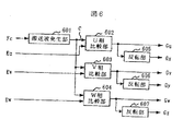
図6は、PWM制御部6の構成を示す回路図である。搬送波発生部601、U相比較部602、V相比較部603、W相比較部604および反転部605、606、607を有する。搬送波発生部601は、搬送波周波数指令Fcに基づいて、周波数Fcの三角波である搬送波Cを出力する。ゲート信号Guを出力するU相比較部602は、U相交流電圧指令信号Euと搬送波Cを比較して、U相交流電圧指令信号Euが大きいときはHレベルを出力し、小さいときはLレベルを出力する。また、ゲート信号Gxを出力する反転部605は、ゲート信号GuがLレベルのときHレベルを出力し、ゲート信号GuがHレベルのときLレベルを出力する。
【0054】
同様に、ゲート信号Gvを出力するV相比較部603は、V相交流電圧指令信号Evと搬送波Cを比較して、又、ゲート信号Gwを出力するW相比較部604は、W相交流電圧指令信号Ewと搬送波Cを比較して、U相比較部602と同様に出力する。また、ゲート信号Gyを出力する反転部606及びゲート信号Gzを出力する反転部607は、ゲート信号Gxと同様に出力する。
【0055】
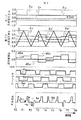
図7は、本実施例の具体的動作を説明する図である。図7に示すグラフは横軸は時間で、縦軸は各々第1の交流電圧指令信号Eu、Ev、及びEw、第2の交流電圧指令信号Eu'、Ev'及びEw'とパルス幅変調の搬送波C、誤差積算値dEu、dEv及びdEw、ゲート信号Gu、Gv、及びGw、直流電流Idcである。
【0056】
第1の交流電圧指令信号Eu、Ev、及びEwは、図1に示す電圧指令補正部6の入力信号であり、それらの値はそれぞれ0.3、-0.1及び-0.3である。第2の交流電圧指令信号Eu'、Ev'及びEw'は第1の交流電圧指令信号Eu、Ev、及びEwに基づいて各々の差を予め定められた値(0.3)以上に補正されたものであり、図に示すように各信号ともに逐次変化している。
【0057】
誤差積算値dEu、dEv及びdEwは、第1の交流電圧指令信号Eu、Ev、及びEwと第2の交流電圧指令信号Eu'、Ev'及びEw'との差の積算値であり、その初期値はそれぞれ0.0、0.0、及び0.1である場合を示している。また、最低電圧Eminは0.3であり、誤差積算値dEu、dEv及びdEwの絶対値はいずれも所定値以上である。
【0058】
例として、時刻T1における電圧指令補正部9の動作は以下の通りである。図3の処理300において、第3の交流電圧指令信号Eu0、Ev0、及びEw0には、それぞれ0.3、-0.1、-0.2を代入する。このとき、Eu0>Ev0>Ew0であるから図3の処理301、処理302を経て処理303を実行する。処理303において、第1の最大電圧Eaには0.3、第1の中間電圧Ebには-0.1、第1の最小電圧Ecには-0.2を代入する。次に、図3の補正処理304、即ち図5に示す補正処理を実行する。
【0059】
補正処理304では、図5の処理501において、Ea-Eb=0.4と最低電圧Emin=0.3を比較する。Ea-EbがEmin以上であるから、処理502を実行し、第2の最大電圧Ea'には0.3を代入する。次の処理504では、Eb-Ec=0.1と最低電圧Emin=0.3を比較して、Eb-EcがEmin未満であるから、処理506を実行する。処理506では、第2の最小電圧Ec'に-0.4を代入する。処理507では、第2の中間電圧Eb'に-0.1を代入し、補正処理が終了する。
【0060】
次に図3の処理305を実行し、第2の交流電圧指令信号Eu'、Ev'及びEw'に、それぞれ0.3、-0.1、-0.4を代入する。次の処理313において、誤差積算値dEu、dEv及びdEwはそれぞれ0.0、0.0、-0.2に更新される。
【0061】
以上説明した電圧指令補正部9の出力する第2の交流電圧指令信号Eu'、Ev'及びEw'と、搬送波Cに基づき、PWM制御部6においてパルス幅変調を行う。PWM制御部6では、搬送波Cと変調波である第2の交流電圧指令信号Eu'、Ev'及びEw'の大きさをそれぞれ比較し、変調波の方が大きい場合は対応するゲート信号にHレベルを、小さい場合はLレベルを出力する。
【0062】
よって、時刻T1〜T2の期間では、ゲート信号Gu、Gv及びGwがすべてLレベルの状態から、はじめにU相ゲート信号GuがHレベルに変わり、第2のU相交流電圧指令信号Eu'と第2のV相交流電流指令Ev'の差に相当する時間だけ遅れて、V相ゲート信号GvがHレベルに変わる。その後、第2のV相交流電圧指令信号Ev'と第2のW相交流電流指令Ew'の差に相当する時間だけ遅れて、W相ゲート信号GwがHレベルに変わる。よって、第2の交流電圧指令信号Eu'、Ev'、及びEw'の相互の差が最低電圧Emin以上であることから、任意のゲート信号が変化した後、他のゲート信号が変化するまでには、少なくとも最低電圧Eminに相当する時間が確保される。
【0063】
次に時刻T1〜T2の期間における、直流電流Idcとゲート信号の関係を説明する。図7では、U相モータ電流Iu及びV相モータ電流Ivが正、W相モータ電流Iwが負の場合を示している。ゲート信号Gu、Gv、及びGwがすべてLレベルの状態では、ゲート信号Gx、Gy、GzはすべてHである。このとき、スイッチング素子Qu、Qv、QwがOFF状態、スイッチング素子Qx、Qy、QzがON状態であるから、電流はスイッチング素子Qx及びQyからモータ4に流れ、モータ4からスイッチング素子Qzに流れ、再びスイッチング素子Qu及びQyに戻ってくる。このため、直流側には電流が流れず、直流電流Idcは0である。
【0064】
次に、U相ゲート信号GuがHレベルに変わると、X相ゲート信号GxはLレベルに変わり、スイチング素子QuがON状態、スイッチング素子QxがOFF状態になる。このとき、電流は平滑コンデンサ3の正極から、スイッチング素子Quを経てモータ4に流れ、モータ4からスイッチング素子Qy、Qzを経て平滑コンデンサ3の負極に流れる。よって、直流電流IdcにはU相モータ電流Iuと同じ電流が流れる。よって、この期間に直流電流を検出するとU相モータ電流Iuが検出できる。
【0065】
次に、V相ゲート信号GvがHレベルに変わると、Y相ゲート信号GyはLレベルに変わり、スイチング素子QvがON状態、スイッチング素子QyがOFF状態になる。このとき、電流は平滑コンデンサ3の正極から、スイッチング素子Qu、Qvを経てモータ4に流れ、モータ4からスイッチング素子Qzを経て平滑コンデンサ3の負極に流れる。よって、直流電流IdcにはW相モータ電流Iwと大きさが同じで極性が反転した電流が流れる。よって、この期間に直流電流を検出するとW相モータ電流Iwが検出できる。
【0066】
次に、W相ゲート信号GwがHレベルに変わると、Z相ゲート信号GzはLレベルに変わり、スイチング素子QwがON状態、スイッチング素子QzがOFF状態になる。このときは、ゲート信号Gu、Gv、及びGwがすべてLレベルの時と同様、直流電流Idcは0である。
【0067】
よって、ゲート信号GuがLレベルからHレベルに変化してから、ゲート信号GvがLレベルからHレベルに変化するまでの期間及びゲート信号GvがLレベルからHレベルに変化してから、ゲート信号GwがLレベルからHレベルに変化するまでの期間が、直流電流Idcを検出するのに十分な時間だけ確保される必要がある。この期間は、第2のU相交流電圧指令信号Eu'と第2のV相交流電圧指令信号Ev'の差及び第2のV相交流電圧指令信号Ev'と第2のW相交流電圧指令信号Ew'の差により決まるため、これらの差が最低電圧Emin以上になるように補正される場合、最低電圧Eminを直流電流Idcを検出するのに十分な時間に相当する値に設定することにより、直流電流Idcを検出する期間が確保できる。
【0068】
また、時刻T1〜8の期間での第2の交流電圧指令信号Eu'、Ev'、及びEw'の平均はそれぞれ0.33、-0.10、-0.29であり、第1の交流電圧指令信号Eu、Ev、Ewとほぼ等しくなる。また、第2の交流電圧指令信号Eu'、Ev'、及びEw'の平均と第1の交流電圧指令信号Eu、Ev、Ewの間の誤差は、W相誤差積算値dEuが0.1であること、時刻T7〜T8でのU相誤差積算値dEuが0.2であることにより管理されている。
【0069】
更に,図7からも明らかなように誤差積算値dEu,dEv,及びdEwの絶対値はある値以下になる。
【0070】
本実施例では,補正による電圧誤差を抑制するため誤差積算値を用いているが,電圧誤差に対する要求が厳しくない用途においては,誤差積算値に関する処理を省略できる。具体的には,図3の処理300における誤差積算値dEu,dEv,及びdEwを0として,第3の交流電圧指令信号Eu0、Ev0、及びEw0として第1の交流電圧指令信号Eu、Ev、及びEwを用い,処理313を省略することにより実現される。これにより,処理を削減することができる。この場合,電圧指令補正部9では、第1の交流電圧指令信号Eu、Ev、及びEwに基づき,第2の交流電圧指令信号Eu'、Ev'、及びEw'のうちの任意の2つの交流電圧指令信号の差が予め定められた値以上になるよう処理を行うことになる。
【0071】
本実施例によれば、直流電流Idcのパルス幅は必ず電流検出が可能な幅が確保され、任意スイッチングと任意スイッチングの間に必要な期間が確保されるため、スイッチングの相互干渉は発生しない。又、本実施例においては、小容量インバータのモータ電流のCTレス化とその電流検出の高性能化、汎用化、大容量でのスイッチング素子の保護が得られ、低速での電流検出を安定に行うことができる。
【0072】
更に、本実施例においては、低電圧、高キャリアでも直流電流をサンプルしホールドでき、他相スイッチングに伴う狭幅リカバリを防止することができる。
【0073】
又、本実施例によれば、任意の2相の変調波の差を最低値以上にすることができるため、パルス幅変調した結果であるパルス出力において、任意の2つのパルスが変化する間隔を最低値に相当する時間以上にできる。また、このパルス幅変調方式を電力変換器に適用することにより、直流電流のパルス幅も最低値に相当する時間以上となるため、直流電流の検出が可能になる。
【0074】
更に、直流電流の電流パルス幅が必ず電流検出が可能な幅以上に確保されることから、補正結果の更新を搬送波の半周期の整数倍にしても、電流検出に支障は来さないため、演算周期を大きくすることができ、パルス幅変調方法の単位時間あたりの演算量を低減でき、又パルスが変化する間隔が確保されるため、スイッチングの相互干渉が発生しないパルス幅変調が得られる。
【0075】
(実施例2)
図8は、電圧指令補正部が出力である第2の交流電圧指令信号Eu'、Ev'、及びEw'を更新するタイミングを変更した例を示す図である。図8において、201はPWM制御部6のパルス幅変調で用いる搬送波、801〜804は電圧指令補正部9が出力を更新するタイミングである。電圧指令補正部9は搬送波201の1周期毎に第2の交流電圧指令信号Eu'、Ev'、及びEw'を出力する。本実施例では、直流電流Idcのパルス幅は必ず確保されることから、搬送波の半周期で必ず電流検出を行うことができる。このため、図8に示すように出力タイミングを1周期に一度にした場合においても、電流検出には何ら問題はない。さらに、電圧指令信号の更新周期が長くなることが問題にならない範囲で、出力タイミングの周期を搬送波の半周期の整数倍で伸ばすことが可能である。これにより、電圧指令補正部9の演算周期も長くすることが可能となり、単位時間あたりの演算量の低減を図ることができる。他、実施例1と同様の効果が得られる。
【0076】
【発明の効果】
本発明によれば、直流電流の電流パルス幅が必ず電流検出が可能な幅以上に確保され、スイッチングの相互干渉が発生しないパルス幅変調方法とその装置及び電力変換方法と電力変換器を提供することができる。
【図面の簡単な説明】
【図1】本発明のパルス幅変調装置の構成図。
【図2】電圧指令補正部の第2の交流電圧指令信号を更新するタイミングを示す図。
【図3】電圧指令補正部の処理手順を示すフロー図。
【図4】電圧指令補正部の処理手順を示すフロー図。
【図5】図3及び図4の補正処理部の処理手順を示すフロー図。
【図6】本発明に係るPWM制御部の構成を示す回路図。
【図7】本発明のパルス幅変調方法の動作例を示す図。
【図8】電圧指令補正部の第2の交流電圧指令信号を更新するタイミングを示す図。
【符号の説明】
1…交流電源、2…整流回路、3…平滑コンデンサ、4…モータ、5…電流検出器、6…PWM制御部、7…電流検出部、8…モータ制御部、9…電圧指令補正部、10…電力変換器、Qu、Qv、Qw、Qx、Qy及びQz…スイッチング素子。[0001]
TECHNICAL FIELD OF THE INVENTION
The present invention relates to a novel pulse width modulation method and apparatus for controlling a power converter, a power conversion method, and a power converter.
[0002]
[Prior art]
[Non-Patent Document 1] Derivation of motor line-current waveforms from the DC-link current of an inverter "IEE PROCEEDING, Vol.136, Pt.B, JULY 1989, pp.196-204
[Patent Document 1] JP-A-2001-327173
[Patent Document 2] JP-A-2002-119062
[Patent Document 3] JP-A-2002-95263
[0003]
In a power converter that converts a direct current into an alternating current by pulse width modulation, there is a method described in
[0004]
[Problems to be solved by the invention]
In
[0005]
Further, in the methods described in
[0006]
As described above, in the conventional power converter using pulse width modulation for converting DC to AC, when detecting the output current of the power converter from the DC current Idc, when the voltage command signal between phases is small, the DC current The pulse width of Idc is narrow, making detection difficult.
[0007]
SUMMARY OF THE INVENTION An object of the present invention is to provide a pulse width modulation method, an apparatus, a power conversion method, and a power converter, in which a current pulse width on the DC side can be made larger than a width capable of current detection and no switching mutual interference occurs. Is to do.
[0008]
[Means for Solving the Problems]
According to the present invention, the second command signal is set so that any two or three of the three command signal differences in the three first command signals are each equal to or greater than a predetermined value. The pulse width modulation method includes a step of performing an operation and a step of performing pulse width modulation based on the second command signal.
[0009]
More specifically, the present invention relates to a pulse width modulation method for performing pulse width modulation on three second command signals calculated based on three first command signals, wherein a difference between any two second command signals is determined. Also, the three error integrated values, which are the integrated values of the differences between the three first command signals and the three second command signals, are all equal to or greater than a predetermined value and are equal to or less than a predetermined value. Calculating the second command signal based on the first command signal; and performing pulse width modulation on the second command signal. The three first command signals and the three first command signals Adding three error integrated values, which are the integrated values of the differences between the three second command signals based on the signals, to the three first command signals to calculate three third command signals; Difference between the two third command signals Characterized by a step of calculating the second command signal so that the above predetermined value.
[0010]
According to the present invention, as a power conversion method, a voltage command signal correcting step of calculating a second AC voltage command signal based on a first AC voltage command signal, and performing a pulse width modulation based on the second AC voltage command signal to generate a gate signal A PWM control step of outputting, and a step of switching a DC voltage based on the gate signal and converting the DC voltage into an AC voltage, wherein the pulse width modulation is performed by the pulse width modulation method described above. And a motor control step of outputting the first AC voltage command signal based on the speed command signal given from the controller.
[0011]
The present invention provides a correction means for calculating a difference between two arbitrary command signals in three command signals to be equal to or more than a predetermined value, and a pulse width modulation means for pulse width modulating the calculated output. Wherein the pulse width modulation device comprises:
[0012]
Also, the present invention provides a pulse width modulation device having pulse width modulation means for pulse width modulating three second command signals calculated based on three first command signals, wherein any two of the second command signals are The second command is set such that the difference between the command signals is equal to or greater than a predetermined value and the integrated value of the difference between each of the three first command signals and the three second command signals is equal to or less than a predetermined value. Signal correcting means, and three error integrated values which are integrated values of differences between three first command signals and three second command signals corrected based on the three first command signals. To the three first command signals to calculate three third command signals, and the second command signal so that any two third command signal differences are equal to or greater than a predetermined value. Correction means for correcting To.
[0013]
The present invention provides a voltage command correction unit that calculates a second AC voltage command signal based on a first AC voltage command signal, and a PWM control unit that performs pulse width modulation based on the second AC voltage command signal and outputs a gate signal And a switching element for switching a DC voltage based on the gate signal to convert the DC voltage to an AC voltage. The power converter for converting a DC voltage to an AC voltage performs the pulse width modulation by the pulse width modulation device described above. It is characterized by the following.
[0014]
That is, according to the present invention, the difference between any two modulated waves in the difference between each of the three input signals can be made equal to or more than the minimum value. The interval at which one pulse changes can be made longer than the time corresponding to the minimum value. In addition, by applying this pulse width modulation method to the power converter, the pulse width of the DC current is also equal to or longer than the time corresponding to the minimum value, so that the DC current can be detected, and the current pulse width on the DC side can be detected. Can always be greater than or equal to the width that allows current detection. Further, since the interval at which the pulse changes is ensured, mutual interference of switching can be suppressed.
[0015]
Further, the three signals and their respective error integrated values are added, and the difference between any two command signals of the addition result is corrected so as to be equal to or more than a minimum value. Pulse width modulation is performed based on the correction result. A pulse width modulation method for updating the error integrated value from the difference between the addition results of the adding means is preferable.
[0016]
Further, since the pulse width of the DC current is always ensured, even if the correction result is updated every half cycle of the carrier wave or an integral multiple thereof, the current detection will not be hindered. Thus, the amount of calculation per unit time of the pulse width modulation method can be reduced. Preferably, the command signal is a voltage command signal, and an error generated by the correction is added to the voltage command signal.
[0017]
BEST MODE FOR CARRYING OUT THE INVENTION
(Example 1)
FIG. 1 is a configuration diagram showing an example of a power converter using the pulse width modulation method of the present invention. In FIG. 1, a
[0018]
The voltage supplied from the
[0019]
The
[0020]
The voltage
[0021]
In this embodiment, the DC voltage is generated from the
[0022]
The voltage
[0023]
Specifically, the voltage
[0024]
The voltage
[0025]
FIG. 3 is a diagram illustrating a flow of performing a main process of the voltage command correction unit. First, the voltage
[0026]
In process 301, the third U-phase AC voltage command signal Eu0 is compared with the third V-phase AC voltage command signal Ev0. If Eu0 is equal to or greater than Ev0, process 302 is executed, and Eu0 is less than Eu0. In this case, the
[0027]
In process 302, the third V-phase AC voltage command signal Ev0 is compared with the third W-phase AC voltage command signal Ew0, and if Ev0 is equal to or greater than Ew0, process 303 is executed, and Ev0 is less than Ew0. If so, the process 306 is executed.
[0028]
In the process 303, the third U-phase AC voltage command signal Eu0 is set to the first maximum voltage Ea, the third V-phase AC voltage command signal Ev0 is set to the first intermediate voltage Eb, and the third W-phase AC voltage command The
[0029]
After the
[0030]
In the process 313, the U-phase error integrated value dEu is obtained by subtracting the second U-phase AC voltage command signal Eu ′ from the third U-phase AC voltage command signal Eu0, and the third V-phase AC voltage command signal Ev0 Is subtracted from the second V-phase AC voltage command signal Ev ', and the V-phase error integrated value dEv is subtracted from the third W-phase AC voltage command signal Ew0. The W-phase error integrated values dEw are updated with the values thus obtained, and the processing of the voltage
[0031]
When the process 306 is executed after the process 302, the process 306 compares the third U-phase AC voltage command signal Eu0 with the third W-phase AC voltage command signal Eu0, and when Eu0 is equal to or greater than Eu0. Executes the
[0032]
When the
[0033]
After the
[0034]
When the
[0035]
After the process 311, a process 312 is executed to convert the second maximum voltage Ea ′ into the second W-phase AC voltage command signal Ew ′ and the second intermediate voltage Eb ′ into the second U-phase AC voltage command signal Eu. , The second minimum voltage Ec ′ is substituted for the second V-phase AC voltage command signal Ev ′, and the process 313 is executed, and the process of the voltage
[0036]
FIG. 4 is a diagram showing another part of the flow of performing the main processing of the voltage
[0037]
In
[0038]
After the
[0039]
In the
[0040]
In
[0041]
After the
[0042]
In the
[0043]
After the
[0044]
By the above processing, of the third AC voltage command signals Eu0, Ev0, and Ew0, the maximum value is the first maximum voltage Ea, the middle value is the first intermediate voltage Eb, and the minimum value is the first intermediate voltage Eb. Substitution is performed for each of the minimum voltages Ec of 1 to execute a correction process. The second maximum voltage Ea ′, the second intermediate voltage Eb ′, and the second minimum voltage Ec ′, which are the execution results of the correction processing, are determined according to the magnitude relationship of the third AC voltage command signals Eu0, Ev0, and Ew0, Substitute for the second AC voltage command signals Eu ', Ev', and Ew '. Further, errors between the first AC voltage command signals Eu, Ev, and Ew and the second AC voltage command signals Eu ′, Ev ′, and Ew ′ due to the correction are error integrated values dEu, dEv, and dEw. By performing processing with the third AC voltage command signals Eu0, Ev0, and Ew0 to which the error integrated values dEu, dEv, and dEw are added, the error integrated value is calculated including the error up to the previous time. Will not continue to increase.
[0045]
FIG. 5 is a diagram showing the flow of the correction process executed in the
[0046]
In the correction processing, in the first processing 501, the difference between the first maximum voltage Ea and the first intermediate voltage Eb is compared with the minimum voltage Emin. If the difference between Ea and Eb is equal to or more than Emin, the
[0047]
In the
[0048]
In the
[0049]
In the
[0050]
In the
[0051]
By the correction processing described above, the difference between the second maximum voltage Ea 'and the second intermediate voltage Eb' and the difference between the second intermediate voltage Eb 'and the second minimum voltage Ec' are equal to or higher than the minimum voltage Emin. Further, since the magnitude relationship does not change before and after the correction, the second maximum voltage Ea ′ ≧ the second intermediate voltage Eb ′ ≧ the second minimum voltage Ec ′. Note that the minimum voltage Emin is used for the value to be added to the first intermediate voltage Eb in the
[0052]
Further, the difference between the maximum value (Ea) and the intermediate value (Eb) is equal to or greater than a certain value (Emin), and the difference between the intermediate value (Eb) and the minimum value (Ec) is equal to or greater than a certain value (Emin). The difference between Ea) and the minimum value (Ec) is equal to or greater than a certain value (Emin). In the present embodiment, each of the three command signal differences in the first AC voltage command signal is equal to or greater than a predetermined value.
[0053]
FIG. 6 is a circuit diagram showing a configuration of the
[0054]
Similarly, V-
[0055]
FIG. 7 is a diagram illustrating a specific operation of the present embodiment. In the graph shown in FIG. 7, the horizontal axis represents time, and the vertical axis represents the first AC voltage command signals Eu, Ev, and Ew, the second AC voltage command signals Eu ′, Ev ′, and Ew ′, and the pulse width modulation. The carrier C, error integrated values dEu, dEv, and dEw, gate signals Gu, Gv, and Gw, and DC current Idc.
[0056]
The first AC voltage command signals Eu, Ev, and Ew are input signals of the voltage
[0057]
The error integrated values dEu, dEv, and dEw are the integrated values of the differences between the first AC voltage command signals Eu, Ev, and Ew and the second AC voltage command signals Eu ′, Ev ′, and Ew ′. The values are 0.0, 0.0, and 0.1, respectively. The minimum voltage Emin is 0.3, and the absolute values of the error integrated values dEu, dEv, and dEw are all equal to or greater than a predetermined value.
[0058]
As an example, the operation of the voltage
[0059]
In the
[0060]
Next, the
[0061]
Based on the second AC voltage command signals Eu ′, Ev ′ and Ew ′ output from the voltage
[0062]
Therefore, in the period from time T1 to T2, the gate signals Gu, Gv, and Gw are all at the L level, the U-phase gate signal Gu first changes to the H level, and the second U-phase AC voltage command signal Eu ′ and the The V-phase gate signal Gv changes to the H level after a delay corresponding to the difference between the two V-phase AC current commands Ev '. Thereafter, the W-phase gate signal Gw changes to the H level after a delay corresponding to the difference between the second V-phase AC voltage command signal Ev 'and the second W-phase AC current command Ew'. Therefore, since the difference between the second AC voltage command signals Eu ′, Ev ′, and Ew ′ is equal to or more than the minimum voltage Emin, after any gate signal changes, the other gate signals change. At least a time corresponding to the minimum voltage Emin is secured.
[0063]
Next, the relationship between the DC current Idc and the gate signal during the period from time T1 to T2 will be described. FIG. 7 shows a case where the U-phase motor current Iu and the V-phase motor current Iv are positive and the W-phase motor current Iw is negative. When the gate signals Gu, Gv, and Gw are all at the L level, the gate signals Gx, Gy, Gz are all at the H level. At this time, since the switching elements Qu, Qv, and Qw are in the OFF state and the switching elements Qx, Qy, and Qz are in the ON state, current flows from the switching elements Qx and Qy to the motor 4, flows from the motor 4 to the switching element Qz, It returns to the switching elements Qu and Qy again. Therefore, no current flows on the DC side, and the DC current Idc is zero.
[0064]
Next, when the U-phase gate signal Gu changes to H level, the X-phase gate signal Gx changes to L level, the switching element Qu is turned on, and the switching element Qx is turned off. At this time, the current flows from the positive electrode of the smoothing
[0065]
Next, when the V-phase gate signal Gv changes to H level, the Y-phase gate signal Gy changes to L level, and the switching element Qv is turned on and the switching element Qy is turned off. At this time, current flows from the positive electrode of the smoothing
[0066]
Next, when the W-phase gate signal Gw changes to the H level, the Z-phase gate signal Gz changes to the L level, the switching element Qw is turned on, and the switching element Qz is turned off. At this time, the DC current Idc is 0 as in the case where the gate signals Gu, Gv, and Gw are all at the L level.
[0067]
Therefore, the period from when the gate signal Gu changes from the L level to the H level until the gate signal Gv changes from the L level to the H level, and after the gate signal Gv changes from the L level to the H level, A period until Gw changes from the L level to the H level needs to be secured for a time sufficient to detect the DC current Idc. During this period, the difference between the second U-phase AC voltage command signal Eu ′ and the second V-phase AC voltage command signal Ev ′ and the second V-phase AC voltage command signal Ev ′ and the second W-phase AC voltage command Since these differences are corrected so as to be equal to or higher than the minimum voltage Emin, the minimum voltage Emin is set to a value corresponding to a time sufficient to detect the DC current Idc. , A period for detecting the DC current Idc can be secured.
[0068]
The averages of the second AC voltage command signals Eu ′, Ev ′, and Ew ′ during the period from time T1 to time T8 are 0.33, −0.10, −0.29, respectively, and the first AC voltage command signals Eu, Ev , Ew. The error between the average of the second AC voltage command signals Eu ', Ev', and Ew 'and the first AC voltage command signals Eu, Ev, Ew is that the W-phase error integrated value dEu is 0.1. , And the U-phase error integrated value dEu between times T7 and T8 is 0.2.
[0069]
Further, as is apparent from FIG. 7, the absolute values of the error integrated values dEu, dEv, and dEw become smaller than a certain value.
[0070]
In this embodiment, the error integrated value is used to suppress the voltage error due to the correction. However, in applications where the demand for the voltage error is not strict, the processing relating to the error integrated value can be omitted. Specifically, the error integrated values dEu, dEv, and dEw in the
[0071]
According to the present embodiment, the pulse width of the DC current Idc always has a width capable of detecting the current, and a necessary period between the arbitrary switchings is ensured, so that no switching mutual interference occurs. Also, in this embodiment, the motor current of the small-capacity inverter can be made CT-less, and the performance of the current detection can be improved, generalized, and the protection of the switching element with a large capacity can be obtained. It can be carried out.
[0072]
Further, in the present embodiment, a DC current can be sampled and held even at a low voltage and a high carrier, and a narrow recovery accompanying the other-phase switching can be prevented.
[0073]
Further, according to the present embodiment, the difference between any two-phase modulated waves can be made equal to or more than the minimum value. Therefore, in the pulse output obtained as a result of the pulse width modulation, the interval at which any two pulses change is determined. It can be longer than the time corresponding to the minimum value. Further, by applying this pulse width modulation method to the power converter, the pulse width of the DC current is also equal to or longer than the time corresponding to the minimum value, so that the DC current can be detected.
[0074]
Further, since the current pulse width of the DC current is always ensured to be equal to or greater than the width capable of detecting the current, even if the update of the correction result is an integral multiple of a half cycle of the carrier wave, the current detection is not hindered. The operation cycle can be increased, the amount of operation per unit time of the pulse width modulation method can be reduced, and the interval at which the pulse changes is secured, so that pulse width modulation that does not cause switching interference can be obtained.
[0075]
(Example 2)
FIG. 8 is a diagram illustrating an example in which the timing of updating the second AC voltage command signals Eu ′, Ev ′, and Ew ′ output from the voltage command correction unit is changed. 8,
[0076]
【The invention's effect】
According to the present invention, there is provided a pulse width modulation method, an apparatus, a power conversion method, and a power converter in which a current pulse width of a direct current is always ensured to be equal to or greater than a width capable of detecting a current and no mutual interference of switching occurs. be able to.
[Brief description of the drawings]
FIG. 1 is a configuration diagram of a pulse width modulation device according to the present invention.
FIG. 2 is a diagram showing timing for updating a second AC voltage command signal of a voltage command correction unit.
FIG. 3 is a flowchart showing a processing procedure of a voltage command correction unit.
FIG. 4 is a flowchart showing a processing procedure of a voltage command correction unit.
FIG. 5 is a flowchart showing a processing procedure of a correction processing unit in FIGS. 3 and 4;
FIG. 6 is a circuit diagram showing a configuration of a PWM control unit according to the present invention.
FIG. 7 is a diagram showing an operation example of the pulse width modulation method of the present invention.
FIG. 8 is a diagram showing timing for updating a second AC voltage command signal of a voltage command correction unit.
[Explanation of symbols]
REFERENCE SIGNS
Claims (13)
Priority Applications (5)
| Application Number | Priority Date | Filing Date | Title |
|---|---|---|---|
| JP2002368421A JP4069741B2 (en) | 2002-12-19 | 2002-12-19 | Pulse width modulation method and power converter |
| TW092119308A TWI227590B (en) | 2002-12-19 | 2003-07-15 | Pulse width modulation method and device thereof, power conversion method and power converter |
| US10/737,999 US7433403B2 (en) | 2002-12-19 | 2003-12-18 | Pulse width modulation method for a power converter |
| DE10360034A DE10360034A1 (en) | 2002-12-19 | 2003-12-19 | Processes for pulse width modulation, pulse width modulator, process for current conversion and current converter |
| US12/246,174 US7920395B2 (en) | 2002-12-19 | 2008-10-06 | Pulse width modulation method for a power converter |
Applications Claiming Priority (1)
| Application Number | Priority Date | Filing Date | Title |
|---|---|---|---|
| JP2002368421A JP4069741B2 (en) | 2002-12-19 | 2002-12-19 | Pulse width modulation method and power converter |
Related Child Applications (1)
| Application Number | Title | Priority Date | Filing Date |
|---|---|---|---|
| JP2006279403A Division JP2007006700A (en) | 2006-10-13 | 2006-10-13 | Power conversion apparatus |
Publications (2)
| Publication Number | Publication Date |
|---|---|
| JP2004201440A true JP2004201440A (en) | 2004-07-15 |
| JP4069741B2 JP4069741B2 (en) | 2008-04-02 |
Family
ID=32677117
Family Applications (1)
| Application Number | Title | Priority Date | Filing Date |
|---|---|---|---|
| JP2002368421A Expired - Fee Related JP4069741B2 (en) | 2002-12-19 | 2002-12-19 | Pulse width modulation method and power converter |
Country Status (4)
| Country | Link |
|---|---|
| US (2) | US7433403B2 (en) |
| JP (1) | JP4069741B2 (en) |
| DE (1) | DE10360034A1 (en) |
| TW (1) | TWI227590B (en) |
Cited By (6)
| Publication number | Priority date | Publication date | Assignee | Title |
|---|---|---|---|---|
| WO2010103733A1 (en) * | 2009-03-09 | 2010-09-16 | 株式会社日立産機システム | Power conversion device, and method for controlling thereof |
| JP2013059246A (en) * | 2011-09-09 | 2013-03-28 | Samsung Electro-Mechanics Co Ltd | Apparatus and method for driving motor with initial correction function |
| JP2013153625A (en) * | 2012-01-26 | 2013-08-08 | Daikin Ind Ltd | Power converter control device |
| JP2013153626A (en) * | 2012-01-26 | 2013-08-08 | Daikin Ind Ltd | Power converter control device |
| JP2013153632A (en) * | 2012-01-26 | 2013-08-08 | Daikin Ind Ltd | Power converter control device |
| JP2013162536A (en) * | 2012-02-01 | 2013-08-19 | Mitsubishi Electric Corp | Power conversion device |
Families Citing this family (9)
| Publication number | Priority date | Publication date | Assignee | Title |
|---|---|---|---|---|
| JP4069741B2 (en) * | 2002-12-19 | 2008-04-02 | 株式会社日立製作所 | Pulse width modulation method and power converter |
| JP2009055748A (en) * | 2007-08-29 | 2009-03-12 | Sanyo Electric Co Ltd | Current detector unit and motor control device |
| US7977898B2 (en) * | 2008-07-21 | 2011-07-12 | GM Global Technology Operations LLC | Current sensing for a multi-phase DC/DC boost converter |
| JP5253470B2 (en) * | 2010-09-13 | 2013-07-31 | 三菱電機株式会社 | Inverter control device |
| JP5737445B2 (en) | 2013-03-05 | 2015-06-17 | ダイキン工業株式会社 | Power converter control device |
| JP5908424B2 (en) * | 2013-03-25 | 2016-04-26 | 日立オートモティブシステムズステアリング株式会社 | Motor control device and power steering device |
| KR20150019187A (en) * | 2013-08-13 | 2015-02-25 | 현대모비스 주식회사 | Vehicle Power Supplying Apparatus |
| US9293978B2 (en) | 2014-01-20 | 2016-03-22 | Cummins Power Generation Ip, Inc. | Split phase power conversion apparatuses, methods and systems |
| JP7064932B2 (en) * | 2018-04-17 | 2022-05-11 | 日立Astemo株式会社 | Inverter control device, inverter control method, inverter control program |
Family Cites Families (5)
| Publication number | Priority date | Publication date | Assignee | Title |
|---|---|---|---|---|
| JP3664040B2 (en) | 2000-05-17 | 2005-06-22 | 日産自動車株式会社 | PWM inverter for motor control |
| JP3610897B2 (en) | 2000-09-14 | 2005-01-19 | 三菱電機株式会社 | INVERTER DEVICE, COMPRESSOR DRIVE DEVICE, REFRIGERATION / AIR CONDITIONER, INVERTER DEVICE CONTROL METHOD |
| JP3665812B2 (en) | 2000-10-03 | 2005-06-29 | 株式会社日立製作所 | Pulse width modulation method, apparatus and power converter |
| JP4045105B2 (en) * | 2002-01-30 | 2008-02-13 | 株式会社日立産機システム | Pulse width modulation method, power conversion device, and inverter device |
| JP4069741B2 (en) * | 2002-12-19 | 2008-04-02 | 株式会社日立製作所 | Pulse width modulation method and power converter |
-
2002
- 2002-12-19 JP JP2002368421A patent/JP4069741B2/en not_active Expired - Fee Related
-
2003
- 2003-07-15 TW TW092119308A patent/TWI227590B/en not_active IP Right Cessation
- 2003-12-18 US US10/737,999 patent/US7433403B2/en active Active
- 2003-12-19 DE DE10360034A patent/DE10360034A1/en not_active Ceased
-
2008
- 2008-10-06 US US12/246,174 patent/US7920395B2/en not_active Expired - Lifetime
Cited By (8)
| Publication number | Priority date | Publication date | Assignee | Title |
|---|---|---|---|---|
| WO2010103733A1 (en) * | 2009-03-09 | 2010-09-16 | 株式会社日立産機システム | Power conversion device, and method for controlling thereof |
| JP2010213407A (en) * | 2009-03-09 | 2010-09-24 | Hitachi Industrial Equipment Systems Co Ltd | Power conversion device and control method thereof |
| US8710781B2 (en) | 2009-03-09 | 2014-04-29 | Hitachi Industrial Equipment Systems Co., Ltd. | Power conversion device and method for controlling thereof |
| JP2013059246A (en) * | 2011-09-09 | 2013-03-28 | Samsung Electro-Mechanics Co Ltd | Apparatus and method for driving motor with initial correction function |
| JP2013153625A (en) * | 2012-01-26 | 2013-08-08 | Daikin Ind Ltd | Power converter control device |
| JP2013153626A (en) * | 2012-01-26 | 2013-08-08 | Daikin Ind Ltd | Power converter control device |
| JP2013153632A (en) * | 2012-01-26 | 2013-08-08 | Daikin Ind Ltd | Power converter control device |
| JP2013162536A (en) * | 2012-02-01 | 2013-08-19 | Mitsubishi Electric Corp | Power conversion device |
Also Published As
| Publication number | Publication date |
|---|---|
| US7920395B2 (en) | 2011-04-05 |
| JP4069741B2 (en) | 2008-04-02 |
| US20090040797A1 (en) | 2009-02-12 |
| TWI227590B (en) | 2005-02-01 |
| US7433403B2 (en) | 2008-10-07 |
| US20040131114A1 (en) | 2004-07-08 |
| TW200414660A (en) | 2004-08-01 |
| DE10360034A1 (en) | 2004-08-05 |
Similar Documents
| Publication | Publication Date | Title |
|---|---|---|
| US7920395B2 (en) | Pulse width modulation method for a power converter | |
| US9484839B2 (en) | Power converter, power generating system, apparatus for controlling power converter, and method for controlling power converter | |
| US9509229B2 (en) | Power supply apparatus including power conversion circuit controlled by PWM control circuit | |
| KR20160122923A (en) | Apparatus and method for generating offset voltage of 3-phase inverter | |
| JP7136314B2 (en) | Power control method and power control device | |
| JP6178433B2 (en) | Power converter | |
| US20150188454A1 (en) | Inverter device, control circuit for inverter device, and method for controlling inverter device | |
| JP2014011944A (en) | Power conversion system and power conversion method | |
| JP2009100505A (en) | 3-level power converter | |
| US10291111B1 (en) | Feedback control for parallel power converter synchronization | |
| JP6131360B1 (en) | Power converter | |
| JP5270272B2 (en) | Inverter control circuit, grid-connected inverter system provided with this inverter control circuit, program for realizing this inverter control circuit, and recording medium recording this program | |
| JP5351390B2 (en) | Power converter | |
| JP2003209976A (en) | Pwm inverter and its current detecting method | |
| JPH03107373A (en) | Power converter and control method thereof | |
| JP2000050529A (en) | Method for limiting current of power converter | |
| JP4493432B2 (en) | Inverter control device | |
| JP6837576B2 (en) | Power converter | |
| JP2007097394A (en) | Electric power transformer | |
| JP2006074951A (en) | Controller for ac motor | |
| JP2007006700A (en) | Power conversion apparatus | |
| JPH10248262A (en) | Power conversion device and its control method | |
| JP2006166664A (en) | Control method of voltage type inverter | |
| JP2014187742A (en) | Inverter device | |
| JP6440067B2 (en) | Power converter |
Legal Events
| Date | Code | Title | Description |
|---|---|---|---|
| A621 | Written request for application examination |
Free format text: JAPANESE INTERMEDIATE CODE: A621 Effective date: 20041004 |
|
| A977 | Report on retrieval |
Free format text: JAPANESE INTERMEDIATE CODE: A971007 Effective date: 20060714 |
|
| A131 | Notification of reasons for refusal |
Free format text: JAPANESE INTERMEDIATE CODE: A131 Effective date: 20060815 |
|
| A521 | Written amendment |
Free format text: JAPANESE INTERMEDIATE CODE: A523 Effective date: 20061016 |
|
| A131 | Notification of reasons for refusal |
Free format text: JAPANESE INTERMEDIATE CODE: A131 Effective date: 20070206 |
|
| A521 | Written amendment |
Free format text: JAPANESE INTERMEDIATE CODE: A523 Effective date: 20070409 |
|
| A02 | Decision of refusal |
Free format text: JAPANESE INTERMEDIATE CODE: A02 Effective date: 20070724 |
|
| A521 | Written amendment |
Free format text: JAPANESE INTERMEDIATE CODE: A523 Effective date: 20070925 |
|
| A911 | Transfer to examiner for re-examination before appeal (zenchi) |
Free format text: JAPANESE INTERMEDIATE CODE: A911 Effective date: 20071113 |
|
| TRDD | Decision of grant or rejection written | ||
| A01 | Written decision to grant a patent or to grant a registration (utility model) |
Free format text: JAPANESE INTERMEDIATE CODE: A01 Effective date: 20071225 |
|
| A61 | First payment of annual fees (during grant procedure) |
Free format text: JAPANESE INTERMEDIATE CODE: A61 Effective date: 20080107 |
|
| R150 | Certificate of patent or registration of utility model |
Free format text: JAPANESE INTERMEDIATE CODE: R150 |
|
| FPAY | Renewal fee payment (event date is renewal date of database) |
Free format text: PAYMENT UNTIL: 20110125 Year of fee payment: 3 |
|
| FPAY | Renewal fee payment (event date is renewal date of database) |
Free format text: PAYMENT UNTIL: 20110125 Year of fee payment: 3 |
|
| FPAY | Renewal fee payment (event date is renewal date of database) |
Free format text: PAYMENT UNTIL: 20120125 Year of fee payment: 4 |
|
| FPAY | Renewal fee payment (event date is renewal date of database) |
Free format text: PAYMENT UNTIL: 20130125 Year of fee payment: 5 |
|
| LAPS | Cancellation because of no payment of annual fees |