JP2004193619A - 光散乱を強化した発光素子 - Google Patents
光散乱を強化した発光素子 Download PDFInfo
- Publication number
- JP2004193619A JP2004193619A JP2003411688A JP2003411688A JP2004193619A JP 2004193619 A JP2004193619 A JP 2004193619A JP 2003411688 A JP2003411688 A JP 2003411688A JP 2003411688 A JP2003411688 A JP 2003411688A JP 2004193619 A JP2004193619 A JP 2004193619A
- Authority
- JP
- Japan
- Prior art keywords
- layer
- textured
- textured layer
- substrate
- light emitting
- Prior art date
- Legal status (The legal status is an assumption and is not a legal conclusion. Google has not performed a legal analysis and makes no representation as to the accuracy of the status listed.)
- Pending
Links
- 238000000149 argon plasma sintering Methods 0.000 title abstract description 5
- 239000000758 substrate Substances 0.000 claims abstract description 54
- 238000000034 method Methods 0.000 claims abstract description 27
- 150000004767 nitrides Chemical class 0.000 claims abstract description 5
- 239000000463 material Substances 0.000 claims description 25
- 229910002704 AlGaN Inorganic materials 0.000 claims description 18
- 229910052594 sapphire Inorganic materials 0.000 claims description 16
- 239000010980 sapphire Substances 0.000 claims description 16
- 239000000203 mixture Substances 0.000 claims description 10
- 238000005530 etching Methods 0.000 claims description 8
- VYPSYNLAJGMNEJ-UHFFFAOYSA-N Silicium dioxide Chemical compound O=[Si]=O VYPSYNLAJGMNEJ-UHFFFAOYSA-N 0.000 claims description 5
- 238000000137 annealing Methods 0.000 claims description 3
- 235000012239 silicon dioxide Nutrition 0.000 claims description 2
- 239000000377 silicon dioxide Substances 0.000 claims description 2
- 238000000151 deposition Methods 0.000 claims 5
- 229910052581 Si3N4 Inorganic materials 0.000 claims 1
- XUIMIQQOPSSXEZ-UHFFFAOYSA-N Silicon Chemical compound [Si] XUIMIQQOPSSXEZ-UHFFFAOYSA-N 0.000 claims 1
- 229910052710 silicon Inorganic materials 0.000 claims 1
- 239000010703 silicon Substances 0.000 claims 1
- HQVNEWCFYHHQES-UHFFFAOYSA-N silicon nitride Chemical compound N12[Si]34N5[Si]62N3[Si]51N64 HQVNEWCFYHHQES-UHFFFAOYSA-N 0.000 claims 1
- 238000004519 manufacturing process Methods 0.000 description 8
- 238000010586 diagram Methods 0.000 description 7
- 239000004065 semiconductor Substances 0.000 description 7
- 239000013078 crystal Substances 0.000 description 6
- 239000002019 doping agent Substances 0.000 description 6
- 230000006911 nucleation Effects 0.000 description 6
- 238000010899 nucleation Methods 0.000 description 6
- 238000005229 chemical vapour deposition Methods 0.000 description 5
- 229910052782 aluminium Inorganic materials 0.000 description 3
- XAGFODPZIPBFFR-UHFFFAOYSA-N aluminium Chemical compound [Al] XAGFODPZIPBFFR-UHFFFAOYSA-N 0.000 description 3
- 239000007789 gas Substances 0.000 description 3
- IJGRMHOSHXDMSA-UHFFFAOYSA-N Atomic nitrogen Chemical compound N#N IJGRMHOSHXDMSA-UHFFFAOYSA-N 0.000 description 2
- GYHNNYVSQQEPJS-UHFFFAOYSA-N Gallium Chemical compound [Ga] GYHNNYVSQQEPJS-UHFFFAOYSA-N 0.000 description 2
- 238000010521 absorption reaction Methods 0.000 description 2
- 230000005540 biological transmission Effects 0.000 description 2
- 230000000694 effects Effects 0.000 description 2
- 238000000605 extraction Methods 0.000 description 2
- 229910052733 gallium Inorganic materials 0.000 description 2
- 229910052751 metal Inorganic materials 0.000 description 2
- 239000002184 metal Substances 0.000 description 2
- 230000003287 optical effect Effects 0.000 description 2
- 238000000059 patterning Methods 0.000 description 2
- 238000004544 sputter deposition Methods 0.000 description 2
- 229910002058 ternary alloy Inorganic materials 0.000 description 2
- -1 thickness Substances 0.000 description 2
- 238000001429 visible spectrum Methods 0.000 description 2
- 230000004888 barrier function Effects 0.000 description 1
- 230000015572 biosynthetic process Effects 0.000 description 1
- 230000008859 change Effects 0.000 description 1
- 230000008878 coupling Effects 0.000 description 1
- 238000010168 coupling process Methods 0.000 description 1
- 238000005859 coupling reaction Methods 0.000 description 1
- 230000007423 decrease Effects 0.000 description 1
- 230000008020 evaporation Effects 0.000 description 1
- 238000001704 evaporation Methods 0.000 description 1
- 238000002513 implantation Methods 0.000 description 1
- 229910052738 indium Inorganic materials 0.000 description 1
- APFVFJFRJDLVQX-UHFFFAOYSA-N indium atom Chemical compound [In] APFVFJFRJDLVQX-UHFFFAOYSA-N 0.000 description 1
- 230000004048 modification Effects 0.000 description 1
- 238000012986 modification Methods 0.000 description 1
- 238000001451 molecular beam epitaxy Methods 0.000 description 1
- 230000000877 morphologic effect Effects 0.000 description 1
- 229910052757 nitrogen Inorganic materials 0.000 description 1
- NJPPVKZQTLUDBO-UHFFFAOYSA-N novaluron Chemical compound C1=C(Cl)C(OC(F)(F)C(OC(F)(F)F)F)=CC=C1NC(=O)NC(=O)C1=C(F)C=CC=C1F NJPPVKZQTLUDBO-UHFFFAOYSA-N 0.000 description 1
- 239000002245 particle Substances 0.000 description 1
- 230000037361 pathway Effects 0.000 description 1
- 239000002243 precursor Substances 0.000 description 1
- 230000008569 process Effects 0.000 description 1
- 230000001902 propagating effect Effects 0.000 description 1
- 229910002059 quaternary alloy Inorganic materials 0.000 description 1
- 230000009467 reduction Effects 0.000 description 1
- 238000007788 roughening Methods 0.000 description 1
- 239000004576 sand Substances 0.000 description 1
- 238000006748 scratching Methods 0.000 description 1
- 230000002393 scratching effect Effects 0.000 description 1
- HBMJWWWQQXIZIP-UHFFFAOYSA-N silicon carbide Chemical compound [Si+]#[C-] HBMJWWWQQXIZIP-UHFFFAOYSA-N 0.000 description 1
- 229910010271 silicon carbide Inorganic materials 0.000 description 1
- 101150077190 sinI gene Proteins 0.000 description 1
- 230000003595 spectral effect Effects 0.000 description 1
- 239000012780 transparent material Substances 0.000 description 1
- 238000002211 ultraviolet spectrum Methods 0.000 description 1
Images


Classifications
-
- H—ELECTRICITY
- H01—ELECTRIC ELEMENTS
- H01L—SEMICONDUCTOR DEVICES NOT COVERED BY CLASS H10
- H01L33/00—Semiconductor devices having potential barriers specially adapted for light emission; Processes or apparatus specially adapted for the manufacture or treatment thereof or of parts thereof; Details thereof
- H01L33/02—Semiconductor devices having potential barriers specially adapted for light emission; Processes or apparatus specially adapted for the manufacture or treatment thereof or of parts thereof; Details thereof characterised by the semiconductor bodies
- H01L33/20—Semiconductor devices having potential barriers specially adapted for light emission; Processes or apparatus specially adapted for the manufacture or treatment thereof or of parts thereof; Details thereof characterised by the semiconductor bodies with a particular shape, e.g. curved or truncated substrate
- H01L33/22—Roughened surfaces, e.g. at the interface between epitaxial layers
Landscapes
- Engineering & Computer Science (AREA)
- Manufacturing & Machinery (AREA)
- Computer Hardware Design (AREA)
- Microelectronics & Electronic Packaging (AREA)
- Power Engineering (AREA)
- Led Devices (AREA)
- Optical Elements Other Than Lenses (AREA)
Abstract
【解決手段】 基板、基板の上に重なるテクスチャ加工層、テクスチャ加工層の上に重なる少なくとも1つのIII族窒化物層、及び、実質的に平面の発光領域を含む発光素子。散乱層を組み込んだ素子は、幾つかの異なる方法によって形成することができる。第1の方法では、エピタキシアル層が堆積され、次にエッチングしてテクスチャ加工層を形成する。第2の方法では、フォトマスクを堆積させ、フォトマスクに開口部を生成するためにパターン化する。次に、フォトマスクに形成した開口内にテクスチャ加工層が選択的に堆積される。第3の方法では、テクスチャ加工層は、三次元の成長に有利な条件下で堆積され、次に任意選択的に焼き鈍しされる。
【選択図】 図2A
Description
テクスチャ加工層を組み込んだ素子は、幾つかの異なる方法によって形成することができる。第1の方法では、エピタキシアル層が堆積され、次にエッチングしてテクスチャ加工層を形成する。第2の方法では、マスクを堆積させ、マスクに開口部を生成するためにパターン化する。次に、マスクに形成した開口内にテクスチャ加工層が選択的に堆積される。第3の方法では、テクスチャ加工層は、三次元の成長に有利な条件下で堆積され、次に任意選択的に焼き鈍しされる。
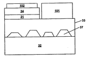
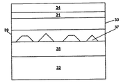
テクスチャ加工層37は、図2Aから図2Cに示されているように活性領域31のn型側か、又は図2Dに示されているように活性領域31のp型側に配置されてもよい。一般的に、活性領域31は平面である。
図2Dは、テクスチャ加工層37が活性領域31のp型側に配置された構造を示している。テクスチャ加工層37は、活性領域31上に直接形成しても良いし、又は、p型領域34の一部分34A又はp型領域34とは別の追加層によって活性領域31から分離されても良い。図2Dに示されている構造の一例では、層34Aは、p型ドープ処理したAlGaN層、テクスチャ加工層37は、AlGaN層、及び、平坦化層39及びp型層24Bは、p型GaN層とすることができる。
三次元及び横方向に成長させる技術は、本明細書において引用により組み込まれる、J・ハン他著「GaN有機金属化学蒸着時の形態進化に対するH2の影響」、応用物理学レター、71(21)、3114〜3116ページ(1997年、11月24日)において更に詳細に検討されている。
当業者には、上述の説明及び添付の図面から、本発明に対する様々な変形が明らかになるであろう。従って、本発明は、特許請求の範囲によってのみ限定されるものとする。
32 基板
33 n型領域
34 p型領域
37 テクスチャ加工層
101 n接点
102 p接点
Claims (32)
- 基板と、
該基板の上に重なるテクスチャ加工層と、
該テクスチャ加工層の上に重なる少なくとも1つのIII族窒化物層と、
実質的に平面の発光領域と、
を含むことを特徴とする発光素子。 - 前記テクスチャ加工層は、前記基板と前記発光領域との間に配置されることを特徴とする請求項1に記載の素子。
- 前記テクスチャ加工層は、前記発光領域の上に重なることを特徴とする請求項1に記載の素子。
- 前記基板は、約2.4よりも小さい屈折率を有することを特徴とする請求項1に記載の素子。
- 前記基板は、サファイアであることを特徴とする請求項1に記載の素子。
- 前記テクスチャ加工層は、光学的に透明であることを特徴とする請求項1に記載の素子。
- 前記少なくとも1つのIII族窒化物層は、前記テクスチャ加工層のテクスチャ加工された表面に隣接し、
該テクスチャ加工層及び該少なくとも1つのIII族窒化物層は、異なる屈折率を有する、
ことを特徴とする請求項1に記載の素子。 - 前記テクスチャ加工層の屈折率は、前記少なくとも1つのIII族窒化物層の屈折率よりも小さいことを特徴とする請求項1に記載の素子。
- 前記テクスチャ加工層は、AlGaNであることを特徴とする請求項1に記載の素子。
- 前記テクスチャ加工層は、約50%から約100%のAl組成を有するAlGaNであることを特徴とする請求項1に記載の素子。
- 前記テクスチャ加工層は、AlNであることを特徴とする請求項1に記載の素子。
- 前記テクスチャ加工層は、アイランドを含む断面を有することを特徴とする請求項1に記載の素子。
- 前記アイランドは、高さが約0.06ミクロンから約10ミクロンであることを特徴とする請求項12に記載の素子。
- 前記アイランドは、高さが約0.06ミクロンから約1ミクロンであることを特徴とする請求項13に記載の素子。
- 前記アイランドは、幅が約0.06ミクロンから約10ミクロンであることを特徴とする請求項13に記載の素子。
- 前記アイランドは、幅が約0.06ミクロンから約1ミクロンであることを特徴とする請求項13に記載の素子。
- 前記テクスチャ加工層は、前記基板に隣接することを特徴とする請求項1に記載の素子。
- 前記テクスチャ加工層の上に重なる共形層を更に含み、
該共形層は、下に重なる該テクスチャ加工層と実質的に共形である、
ことを特徴とする請求項1に記載の素子。 - 前記基板と前記テクスチャ加工層との間に配置されたIII族窒化物層を更に含むことを特徴とする請求項1に記載の素子。
- 前記テクスチャ加工層は、λnを該テクスチャ加工層の前記発光領域によって放射された光の波長とすると、約λn/4に等しいか又はそれ以上の寸法を有する三次元形態を含むことを特徴とする請求項1に記載の素子。
- 前記テクスチャ加工層の上に重なる前記少なくとも1つのIII族窒化物層は、該テクスチャ加工層に隣接する平坦でない表面、及び該テクスチャ加工層の反対側の平面を含むことを特徴とする請求項1に記載の素子。
- n型領域と、
該n型領域とp型領域との間に前記発光領域が配置されるようなp型領域と、
該n型領域上に形成されたn接点と、
該p型領域上に形成されたp接点と、
該n接点及びp接点と電気的に接続されたリードと、
前記発光領域の反対側の前記基板の側面に配置された覆いと、
を更に含むことを特徴とする請求項1に記載の素子。 - 基板の上に重なるテクスチャ加工層を形成する段階と、
該基板の上に重なる実質的に平面の発光領域を形成する段階と、
該テクスチャ加工層の上に重なる少なくとも1つのIII族窒化物層を形成する段階と、
を含むことを特徴とする、発光素子を形成する方法。 - 前記テクスチャ加工層は、III族窒化物材料であることを特徴とする請求項23に記載の方法。
- テクスチャ加工層を形成する段階は、
エピタキシアル材料の層を堆積させる段階と、
三次元表面を形成するために、該エピタキシアル材料の一部分をエッチングで取り除く段階と、
を含むことを特徴とする請求項24に記載の方法。 - 前記エピタキシアル材料の一部分をエッチングで取り除く段階は、H2、N2、NH3、HCl、及びそれらの混合物から成るグループから選択されたエッチャントを用いてエッチングする段階を含むことを特徴とする請求項25に記載の方法。
- テクスチャ加工層を形成する段階は、
III族窒化物材料の層を堆積させる段階と、
該III族窒化物材料の層を焼き鈍しする段階と、
を含むことを特徴とする請求項24に記載の方法。 - 前記III族窒化物材料の一部分をエッチングで取り除く段階を更に含むことを特徴とする請求項27に記載の方法。
- テクスチャ加工層を形成する段階は、
基板の上にマスク層を堆積させる段階と、
該マスク層に複数の開口部を作り出す段階と、
該マスク層の該開口部に前記テクスチャ加工層の少なくとも一部分を堆積させる段階と、
を含むことを特徴とする請求項24に記載の方法。 - 前記マスク層は、二酸化珪素、窒化珪素、及びオキシナイトライド珪素のうちの1つであることを特徴とする請求項29に記載の方法。
- 前記基板は、サファイアであることを特徴とする請求項24に記載の方法。
- テクスチャ加工層を形成する段階は、エピタキシアル材料の三次元層を堆積させる段階を含むことを特徴とする請求項24に記載の方法。
Applications Claiming Priority (1)
| Application Number | Priority Date | Filing Date | Title |
|---|---|---|---|
| US10/317,956 US7071494B2 (en) | 2002-12-11 | 2002-12-11 | Light emitting device with enhanced optical scattering |
Related Child Applications (1)
| Application Number | Title | Priority Date | Filing Date |
|---|---|---|---|
| JP2011183905A Division JP5134119B2 (ja) | 2002-12-11 | 2011-08-25 | 光散乱を強化した発光素子 |
Publications (2)
| Publication Number | Publication Date |
|---|---|
| JP2004193619A true JP2004193619A (ja) | 2004-07-08 |
| JP2004193619A5 JP2004193619A5 (ja) | 2007-02-15 |
Family
ID=32325961
Family Applications (2)
| Application Number | Title | Priority Date | Filing Date |
|---|---|---|---|
| JP2003411688A Pending JP2004193619A (ja) | 2002-12-11 | 2003-12-10 | 光散乱を強化した発光素子 |
| JP2011183905A Expired - Lifetime JP5134119B2 (ja) | 2002-12-11 | 2011-08-25 | 光散乱を強化した発光素子 |
Family Applications After (1)
| Application Number | Title | Priority Date | Filing Date |
|---|---|---|---|
| JP2011183905A Expired - Lifetime JP5134119B2 (ja) | 2002-12-11 | 2011-08-25 | 光散乱を強化した発光素子 |
Country Status (4)
| Country | Link |
|---|---|
| US (1) | US7071494B2 (ja) |
| EP (1) | EP1429396B1 (ja) |
| JP (2) | JP2004193619A (ja) |
| TW (1) | TW200414573A (ja) |
Cited By (11)
| Publication number | Priority date | Publication date | Assignee | Title |
|---|---|---|---|---|
| JP2006140357A (ja) * | 2004-11-12 | 2006-06-01 | Mitsubishi Cable Ind Ltd | 窒化物半導体発光素子 |
| JP2007128925A (ja) * | 2004-09-23 | 2007-05-24 | Philips Lumileds Lightng Co Llc | テクスチャ基板上で成長させるiii族発光素子 |
| JP2007221142A (ja) * | 2006-02-14 | 2007-08-30 | Samsung Electro Mech Co Ltd | 半導体発光素子及びその製造方法 |
| JP2008010809A (ja) * | 2006-06-26 | 2008-01-17 | Tekcore Co Ltd | 光抽出スポットの配列を組み込む発光ダイオード及び発光ダイオードの形成方法 |
| DE112007001207T5 (de) | 2006-05-23 | 2009-04-02 | Alps Electric Co., Ltd. | Verfahren zum Herstellen eines lichtemittierenden Halbleiterelements |
| JP2009176805A (ja) * | 2008-01-22 | 2009-08-06 | Tekcore Co Ltd | 発光ダイオード基板粗面処理の方法 |
| KR101068157B1 (ko) | 2009-05-12 | 2011-09-27 | 전북대학교산학협력단 | 에어패스를 포함하는 발광소자 및 그 제조방법 |
| KR101068158B1 (ko) | 2009-05-12 | 2011-09-27 | 전북대학교산학협력단 | 에어면을 포함하는 발광소자 및 그 제조방법 |
| JP2013048301A (ja) * | 2010-01-08 | 2013-03-07 | Taiwan Semiconductor Manufacturing Co Ltd | 光デバイス |
| CN103390707A (zh) * | 2012-05-08 | 2013-11-13 | 华夏光股份有限公司 | 半导体发光装置及其制造方法 |
| JP2014183285A (ja) * | 2013-03-21 | 2014-09-29 | Stanley Electric Co Ltd | 発光素子 |
Families Citing this family (45)
| Publication number | Priority date | Publication date | Assignee | Title |
|---|---|---|---|---|
| US6900067B2 (en) * | 2002-12-11 | 2005-05-31 | Lumileds Lighting U.S., Llc | Growth of III-nitride films on mismatched substrates without conventional low temperature nucleation layers |
| US7781795B2 (en) * | 2003-12-22 | 2010-08-24 | Showa Denko K.K. | Group III nitride semiconductor device and light-emitting device using the same |
| KR100581831B1 (ko) * | 2004-02-05 | 2006-05-23 | 엘지전자 주식회사 | 발광 다이오드 |
| JP2007533164A (ja) * | 2004-04-15 | 2007-11-15 | トラスティーズ オブ ボストン ユニバーシティ | テクスチャ出しされた半導体層を特徴とする光学装置 |
| US8035113B2 (en) * | 2004-04-15 | 2011-10-11 | The Trustees Of Boston University | Optical devices featuring textured semiconductor layers |
| DE102004050891B4 (de) * | 2004-10-19 | 2019-01-10 | Lumileds Holding B.V. | Lichtmittierende III-Nitrid-Halbleitervorrichtung |
| KR100664988B1 (ko) | 2004-11-04 | 2007-01-09 | 삼성전기주식회사 | 광추출효율이 향상된 반도체 발광소자 |
| US20070145386A1 (en) | 2004-12-08 | 2007-06-28 | Samsung Electro-Mechanics Co., Ltd. | Semiconductor light emitting device and method of manufacturing the same |
| KR100624449B1 (ko) | 2004-12-08 | 2006-09-18 | 삼성전기주식회사 | 요철 구조를 포함하는 발광 소자 및 그 제조 방법 |
| KR101154744B1 (ko) * | 2005-08-01 | 2012-06-08 | 엘지이노텍 주식회사 | 질화물 발광 소자 및 그 제조 방법 |
| WO2007081719A2 (en) | 2006-01-05 | 2007-07-19 | Illumitex, Inc. | Separate optical device for directing light from an led |
| KR20070081184A (ko) | 2006-02-10 | 2007-08-16 | 삼성전기주식회사 | 질화물계 반도체 발광소자 및 그 제조방법 |
| KR100828873B1 (ko) * | 2006-04-25 | 2008-05-09 | 엘지이노텍 주식회사 | 질화물 반도체 발광소자 및 그 제조방법 |
| WO2008042351A2 (en) * | 2006-10-02 | 2008-04-10 | Illumitex, Inc. | Led system and method |
| JP2008124060A (ja) * | 2006-11-08 | 2008-05-29 | Showa Denko Kk | Iii族窒化物化合物半導体発光素子の製造方法、及びiii族窒化物化合物半導体発光素子、並びにランプ |
| JP4433317B2 (ja) * | 2006-12-15 | 2010-03-17 | 豊田合成株式会社 | Iii族窒化物系化合物半導体結晶の製造方法 |
| US7663148B2 (en) * | 2006-12-22 | 2010-02-16 | Philips Lumileds Lighting Company, Llc | III-nitride light emitting device with reduced strain light emitting layer |
| US20080149946A1 (en) * | 2006-12-22 | 2008-06-26 | Philips Lumileds Lighting Company, Llc | Semiconductor Light Emitting Device Configured To Emit Multiple Wavelengths Of Light |
| CN101452982A (zh) * | 2007-11-29 | 2009-06-10 | 富士迈半导体精密工业(上海)有限公司 | 固态发光器件 |
| US7985979B2 (en) | 2007-12-19 | 2011-07-26 | Koninklijke Philips Electronics, N.V. | Semiconductor light emitting device with light extraction structures |
| TW200929593A (en) * | 2007-12-20 | 2009-07-01 | Nat Univ Tsing Hua | Light source with reflective pattern structure |
| US7829358B2 (en) | 2008-02-08 | 2010-11-09 | Illumitex, Inc. | System and method for emitter layer shaping |
| US8592800B2 (en) * | 2008-03-07 | 2013-11-26 | Trustees Of Boston University | Optical devices featuring nonpolar textured semiconductor layers |
| KR101533296B1 (ko) | 2008-07-08 | 2015-07-02 | 삼성전자주식회사 | 패턴 형성 기판을 구비한 질화물 반도체 발광소자 및 그제조방법 |
| TW201034256A (en) | 2008-12-11 | 2010-09-16 | Illumitex Inc | Systems and methods for packaging light-emitting diode devices |
| KR101064082B1 (ko) * | 2009-01-21 | 2011-09-08 | 엘지이노텍 주식회사 | 발광 소자 |
| US8449128B2 (en) | 2009-08-20 | 2013-05-28 | Illumitex, Inc. | System and method for a lens and phosphor layer |
| US8585253B2 (en) | 2009-08-20 | 2013-11-19 | Illumitex, Inc. | System and method for color mixing lens array |
| EP2341558B1 (en) | 2009-12-30 | 2019-04-24 | IMEC vzw | Method of manufacturing a semiconductor device |
| US8203153B2 (en) | 2010-01-15 | 2012-06-19 | Koninklijke Philips Electronics N.V. | III-V light emitting device including a light extracting structure |
| RU2461916C1 (ru) * | 2011-01-12 | 2012-09-20 | Государственное образовательное учреждение высшего профессионального образования Томский государственный университет систем управления и радиоэлектроники (ТУСУР) | Полупроводниковый светоизлучающий прибор |
| RU2504867C2 (ru) * | 2012-01-10 | 2014-01-20 | Федеральное государственное бюджетное образовательное учреждение высшего профессионального образования Томский государственный университет систем управления и радиоэлектроники | Способ изготовления светодиода |
| JP2014056879A (ja) * | 2012-09-11 | 2014-03-27 | Rohm Co Ltd | 半導体発光素子 |
| US20140078722A1 (en) * | 2012-09-19 | 2014-03-20 | Venntis Technologies LLC | Illuminator with device for scattering light |
| CN103094440B (zh) * | 2013-01-11 | 2016-03-09 | 厦门市三安光电科技有限公司 | 氮化物发光二极管及其制作方法 |
| KR20150039926A (ko) * | 2013-10-04 | 2015-04-14 | 엘지이노텍 주식회사 | 발광소자 |
| TWI640104B (zh) * | 2014-05-30 | 2018-11-01 | 日商日亞化學工業股份有限公司 | 氮化物半導體元件及其製造方法 |
| WO2015181671A1 (en) * | 2014-05-30 | 2015-12-03 | Koninklijke Philips N.V. | Light-emitting device with patterned substrate |
| US10516084B2 (en) | 2014-10-31 | 2019-12-24 | eLux, Inc. | Encapsulated fluid assembly emissive elements |
| US20160211431A1 (en) * | 2015-01-21 | 2016-07-21 | Korea Institute Of Science And Technology | Heat radiation sheet, light emitting device, and heat radiation back sheet for photovoltaic module, each including boron nitride heat dissipation layer |
| DE102015109761B4 (de) | 2015-06-18 | 2022-01-27 | OSRAM Opto Semiconductors Gesellschaft mit beschränkter Haftung | Verfahren zur Herstellung eines Nitrid-Halbleiterbauelements und Nitrid-Halbleiterbauelement |
| CN105576096B (zh) * | 2016-03-15 | 2018-08-10 | 河源市众拓光电科技有限公司 | 一种采用SiN插入层在Si衬底上生长的LED外延片的制备方法 |
| KR102587958B1 (ko) * | 2017-02-03 | 2023-10-11 | 삼성전자주식회사 | 메타 광학 소자 및 그 제조 방법 |
| CN111066158B (zh) * | 2017-09-07 | 2022-05-03 | 苏州晶湛半导体有限公司 | 发光器件表面粗化的方法与发光器件 |
| US20210366703A1 (en) * | 2020-05-20 | 2021-11-25 | Asahi Kasei Kabushiki Kaisha | Nitride semiconductor element |
Citations (2)
| Publication number | Priority date | Publication date | Assignee | Title |
|---|---|---|---|---|
| WO2001041225A2 (en) * | 1999-12-03 | 2001-06-07 | Cree Lighting Company | Enhanced light extraction in leds through the use of internal and external optical elements |
| JP2002280611A (ja) * | 2001-03-21 | 2002-09-27 | Mitsubishi Cable Ind Ltd | 半導体発光素子 |
Family Cites Families (26)
| Publication number | Priority date | Publication date | Assignee | Title |
|---|---|---|---|---|
| US5032893A (en) | 1988-04-01 | 1991-07-16 | Cornell Research Foundation, Inc. | Method for reducing or eliminating interface defects in mismatched semiconductor eiplayers |
| JP2953468B2 (ja) * | 1989-06-21 | 1999-09-27 | 三菱化学株式会社 | 化合物半導体装置及びその表面処理加工方法 |
| US4971928A (en) | 1990-01-16 | 1990-11-20 | General Motors Corporation | Method of making a light emitting semiconductor having a rear reflecting surface |
| JP2737563B2 (ja) | 1992-08-18 | 1998-04-08 | 三菱電機株式会社 | 半導体発光装置 |
| EP0952617B1 (en) | 1993-04-28 | 2004-07-28 | Nichia Corporation | Gallium nitride-based III-V group compound semiconductor device |
| TW253999B (ja) | 1993-06-30 | 1995-08-11 | Hitachi Cable | |
| US5631190A (en) | 1994-10-07 | 1997-05-20 | Cree Research, Inc. | Method for producing high efficiency light-emitting diodes and resulting diode structures |
| US5814839A (en) | 1995-02-16 | 1998-09-29 | Sharp Kabushiki Kaisha | Semiconductor light-emitting device having a current adjusting layer and a uneven shape light emitting region, and method for producing same |
| US5779924A (en) | 1996-03-22 | 1998-07-14 | Hewlett-Packard Company | Ordered interface texturing for a light emitting device |
| JP3164016B2 (ja) | 1996-05-31 | 2001-05-08 | 住友電気工業株式会社 | 発光素子および発光素子用ウエハの製造方法 |
| US5929467A (en) | 1996-12-04 | 1999-07-27 | Sony Corporation | Field effect transistor with nitride compound |
| CN1292458C (zh) | 1997-04-11 | 2006-12-27 | 日亚化学工业株式会社 | 氮化物半导体的生长方法、氮化物半导体衬底及器件 |
| US6015979A (en) | 1997-08-29 | 2000-01-18 | Kabushiki Kaisha Toshiba | Nitride-based semiconductor element and method for manufacturing the same |
| JP3955367B2 (ja) | 1997-09-30 | 2007-08-08 | フィリップス ルミレッズ ライティング カンパニー リミテッド ライアビリティ カンパニー | 光半導体素子およびその製造方法 |
| JP3925753B2 (ja) | 1997-10-24 | 2007-06-06 | ソニー株式会社 | 半導体素子およびその製造方法ならびに半導体発光素子 |
| US6091085A (en) | 1998-02-19 | 2000-07-18 | Agilent Technologies, Inc. | GaN LEDs with improved output coupling efficiency |
| US6051849A (en) | 1998-02-27 | 2000-04-18 | North Carolina State University | Gallium nitride semiconductor structures including a lateral gallium nitride layer that extends from an underlying gallium nitride layer |
| US6046465A (en) | 1998-04-17 | 2000-04-04 | Hewlett-Packard Company | Buried reflectors for light emitters in epitaxial material and method for producing same |
| US6291839B1 (en) | 1998-09-11 | 2001-09-18 | Lulileds Lighting, U.S. Llc | Light emitting device having a finely-patterned reflective contact |
| JP3592553B2 (ja) * | 1998-10-15 | 2004-11-24 | 株式会社東芝 | 窒化ガリウム系半導体装置 |
| US6133589A (en) | 1999-06-08 | 2000-10-17 | Lumileds Lighting, U.S., Llc | AlGaInN-based LED having thick epitaxial layer for improved light extraction |
| JP3633447B2 (ja) * | 1999-09-29 | 2005-03-30 | 豊田合成株式会社 | Iii族窒化物系化合物半導体素子 |
| US6410942B1 (en) | 1999-12-03 | 2002-06-25 | Cree Lighting Company | Enhanced light extraction through the use of micro-LED arrays |
| KR100632760B1 (ko) * | 2001-03-21 | 2006-10-11 | 미츠비시 덴센 고교 가부시키가이샤 | 반도체 발광 소자 |
| JP3956637B2 (ja) * | 2001-04-12 | 2007-08-08 | ソニー株式会社 | 窒化物半導体の結晶成長方法及び半導体素子の形成方法 |
| US6563142B2 (en) | 2001-07-11 | 2003-05-13 | Lumileds Lighting, U.S., Llc | Reducing the variation of far-field radiation patterns of flipchip light emitting diodes |
-
2002
- 2002-12-11 US US10/317,956 patent/US7071494B2/en not_active Expired - Lifetime
-
2003
- 2003-11-07 EP EP03104120.5A patent/EP1429396B1/en not_active Expired - Lifetime
- 2003-12-08 TW TW092134565A patent/TW200414573A/zh unknown
- 2003-12-10 JP JP2003411688A patent/JP2004193619A/ja active Pending
-
2011
- 2011-08-25 JP JP2011183905A patent/JP5134119B2/ja not_active Expired - Lifetime
Patent Citations (2)
| Publication number | Priority date | Publication date | Assignee | Title |
|---|---|---|---|---|
| WO2001041225A2 (en) * | 1999-12-03 | 2001-06-07 | Cree Lighting Company | Enhanced light extraction in leds through the use of internal and external optical elements |
| JP2002280611A (ja) * | 2001-03-21 | 2002-09-27 | Mitsubishi Cable Ind Ltd | 半導体発光素子 |
Cited By (11)
| Publication number | Priority date | Publication date | Assignee | Title |
|---|---|---|---|---|
| JP2007128925A (ja) * | 2004-09-23 | 2007-05-24 | Philips Lumileds Lightng Co Llc | テクスチャ基板上で成長させるiii族発光素子 |
| JP2006140357A (ja) * | 2004-11-12 | 2006-06-01 | Mitsubishi Cable Ind Ltd | 窒化物半導体発光素子 |
| JP2007221142A (ja) * | 2006-02-14 | 2007-08-30 | Samsung Electro Mech Co Ltd | 半導体発光素子及びその製造方法 |
| DE112007001207T5 (de) | 2006-05-23 | 2009-04-02 | Alps Electric Co., Ltd. | Verfahren zum Herstellen eines lichtemittierenden Halbleiterelements |
| JP2008010809A (ja) * | 2006-06-26 | 2008-01-17 | Tekcore Co Ltd | 光抽出スポットの配列を組み込む発光ダイオード及び発光ダイオードの形成方法 |
| JP2009176805A (ja) * | 2008-01-22 | 2009-08-06 | Tekcore Co Ltd | 発光ダイオード基板粗面処理の方法 |
| KR101068157B1 (ko) | 2009-05-12 | 2011-09-27 | 전북대학교산학협력단 | 에어패스를 포함하는 발광소자 및 그 제조방법 |
| KR101068158B1 (ko) | 2009-05-12 | 2011-09-27 | 전북대학교산학협력단 | 에어면을 포함하는 발광소자 및 그 제조방법 |
| JP2013048301A (ja) * | 2010-01-08 | 2013-03-07 | Taiwan Semiconductor Manufacturing Co Ltd | 光デバイス |
| CN103390707A (zh) * | 2012-05-08 | 2013-11-13 | 华夏光股份有限公司 | 半导体发光装置及其制造方法 |
| JP2014183285A (ja) * | 2013-03-21 | 2014-09-29 | Stanley Electric Co Ltd | 発光素子 |
Also Published As
| Publication number | Publication date |
|---|---|
| JP2011238972A (ja) | 2011-11-24 |
| US7071494B2 (en) | 2006-07-04 |
| JP5134119B2 (ja) | 2013-01-30 |
| TW200414573A (en) | 2004-08-01 |
| EP1429396A1 (en) | 2004-06-16 |
| EP1429396B1 (en) | 2019-06-19 |
| US20040113163A1 (en) | 2004-06-17 |
Similar Documents
| Publication | Publication Date | Title |
|---|---|---|
| JP5134119B2 (ja) | 光散乱を強化した発光素子 | |
| US10062821B2 (en) | Light-emitting device | |
| JP6275817B2 (ja) | 仮像電子及び光学電子装置に対する平面コンタクト | |
| US8357923B2 (en) | External extraction light emitting diode based upon crystallographic faceted surfaces | |
| US9041005B2 (en) | Solid state lighting devices with cellular arrays and associated methods of manufacturing | |
| US9711687B2 (en) | Light emitting device with improved extraction efficiency | |
| US8574939B2 (en) | Semiconductor optoelectronics structure with increased light extraction efficiency and fabrication method thereof | |
| KR100638730B1 (ko) | 수직구조 3족 질화물 발광 소자의 제조 방법 | |
| US9000450B2 (en) | Grown photonic crystals in semiconductor light emitting devices | |
| TWI317565B (en) | Light emitting diode, method for manufacturing light emitting diode, integrated light emitting diode, method for manufacturing integrated light emitting diode, light emitting diode backlight, light emitting diode illumination device, light emitting diode | |
| US20060060888A1 (en) | Growth of III-nitride light emitting devices on textured substrates | |
| CN105009308B (zh) | 用于创建多孔反射接触件的方法和装置 | |
| US20150102381A1 (en) | Semiconductor light emitting device, wafer, and method for manufacturing nitride semiconductor crystal layer | |
| US9741897B2 (en) | Thin light emitting diode and fabrication method | |
| TW201121099A (en) | Semiconductor light-emitting device and method for manufacturing the same | |
| KR100593912B1 (ko) | 질화갈륨계 반도체 발광소자 및 그 제조 방법 | |
| JP2007242669A (ja) | 半導体発光装置及びその製造方法 | |
| JP2005072092A (ja) | 発光ダイオード装置及びその製造方法 | |
| TW200415802A (en) | Light-emitting diode device | |
| TW200408141A (en) | GaN-based Ⅲ-Ⅴ group compound semiconductor light-emitting diode and the manufacturing method thereof |
Legal Events
| Date | Code | Title | Description |
|---|---|---|---|
| A521 | Request for written amendment filed |
Free format text: JAPANESE INTERMEDIATE CODE: A523 Effective date: 20061211 |
|
| A621 | Written request for application examination |
Free format text: JAPANESE INTERMEDIATE CODE: A621 Effective date: 20061211 |
|
| A131 | Notification of reasons for refusal |
Free format text: JAPANESE INTERMEDIATE CODE: A131 Effective date: 20091214 |
|
| A521 | Request for written amendment filed |
Free format text: JAPANESE INTERMEDIATE CODE: A523 Effective date: 20100315 |
|
| A131 | Notification of reasons for refusal |
Free format text: JAPANESE INTERMEDIATE CODE: A131 Effective date: 20100816 |
|
| A521 | Request for written amendment filed |
Free format text: JAPANESE INTERMEDIATE CODE: A523 Effective date: 20101116 |
|
| A02 | Decision of refusal |
Free format text: JAPANESE INTERMEDIATE CODE: A02 Effective date: 20110425 |
|
| A521 | Request for written amendment filed |
Free format text: JAPANESE INTERMEDIATE CODE: A523 Effective date: 20110825 |