JP2004191355A - 照明及び画像取得システム - Google Patents
照明及び画像取得システム Download PDFInfo
- Publication number
- JP2004191355A JP2004191355A JP2003335093A JP2003335093A JP2004191355A JP 2004191355 A JP2004191355 A JP 2004191355A JP 2003335093 A JP2003335093 A JP 2003335093A JP 2003335093 A JP2003335093 A JP 2003335093A JP 2004191355 A JP2004191355 A JP 2004191355A
- Authority
- JP
- Japan
- Prior art keywords
- light
- imager
- flash
- inspection system
- image
- Prior art date
- Legal status (The legal status is an assumption and is not a legal conclusion. Google has not performed a legal analysis and makes no representation as to the accuracy of the status listed.)
- Pending
Links
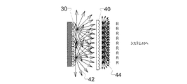
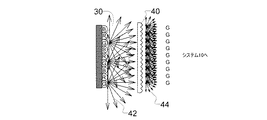
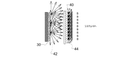
- 238000007689 inspection Methods 0.000 claims abstract description 37
- 230000003287 optical effect Effects 0.000 claims abstract description 29
- 230000007547 defect Effects 0.000 claims abstract description 23
- 239000002131 composite material Substances 0.000 claims abstract description 17
- 238000004519 manufacturing process Methods 0.000 claims abstract description 14
- 238000001228 spectrum Methods 0.000 claims abstract description 12
- 239000000758 substrate Substances 0.000 claims description 29
- 238000005286 illumination Methods 0.000 claims description 28
- 238000000034 method Methods 0.000 claims description 17
- 230000008569 process Effects 0.000 claims description 4
- 230000004044 response Effects 0.000 claims description 2
- 241000098700 Sarcocheilichthys parvus Species 0.000 claims 1
- 241000695776 Thorichthys aureus Species 0.000 claims 1
- 238000001514 detection method Methods 0.000 abstract description 2
- 239000003086 colorant Substances 0.000 description 6
- 238000010586 diagram Methods 0.000 description 6
- 230000003595 spectral effect Effects 0.000 description 6
- 239000011521 glass Substances 0.000 description 4
- 230000002950 deficient Effects 0.000 description 3
- 239000000969 carrier Substances 0.000 description 2
- 230000000052 comparative effect Effects 0.000 description 2
- 230000008859 change Effects 0.000 description 1
- 238000003384 imaging method Methods 0.000 description 1
- 238000000926 separation method Methods 0.000 description 1
- 229910052724 xenon Inorganic materials 0.000 description 1
- FHNFHKCVQCLJFQ-UHFFFAOYSA-N xenon atom Chemical compound [Xe] FHNFHKCVQCLJFQ-UHFFFAOYSA-N 0.000 description 1
Images


Classifications
-
- G—PHYSICS
- G01—MEASURING; TESTING
- G01N—INVESTIGATING OR ANALYSING MATERIALS BY DETERMINING THEIR CHEMICAL OR PHYSICAL PROPERTIES
- G01N21/00—Investigating or analysing materials by the use of optical means, i.e. using sub-millimetre waves, infrared, visible or ultraviolet light
- G01N21/84—Systems specially adapted for particular applications
- G01N21/88—Investigating the presence of flaws or contamination
- G01N21/8806—Specially adapted optical and illumination features
Landscapes
- General Health & Medical Sciences (AREA)
- General Physics & Mathematics (AREA)
- Life Sciences & Earth Sciences (AREA)
- Chemical & Material Sciences (AREA)
- Analytical Chemistry (AREA)
- Biochemistry (AREA)
- Health & Medical Sciences (AREA)
- Immunology (AREA)
- Physics & Mathematics (AREA)
- Pathology (AREA)
- Investigating Materials By The Use Of Optical Means Adapted For Particular Applications (AREA)
- Length Measuring Devices By Optical Means (AREA)
- Testing Or Measuring Of Semiconductors Or The Like (AREA)
- Image Input (AREA)
- Supply And Installment Of Electrical Components (AREA)
Applications Claiming Priority (1)
| Application Number | Priority Date | Filing Date | Title |
|---|---|---|---|
| US10/254,542 US6781687B2 (en) | 2002-09-26 | 2002-09-26 | Illumination and image acquisition system |
Publications (2)
| Publication Number | Publication Date |
|---|---|
| JP2004191355A true JP2004191355A (ja) | 2004-07-08 |
| JP2004191355A5 JP2004191355A5 (enExample) | 2006-11-02 |
Family
ID=32029037
Family Applications (1)
| Application Number | Title | Priority Date | Filing Date |
|---|---|---|---|
| JP2003335093A Pending JP2004191355A (ja) | 2002-09-26 | 2003-09-26 | 照明及び画像取得システム |
Country Status (3)
| Country | Link |
|---|---|
| US (1) | US6781687B2 (enExample) |
| JP (1) | JP2004191355A (enExample) |
| TW (1) | TWI289719B (enExample) |
Cited By (5)
| Publication number | Priority date | Publication date | Assignee | Title |
|---|---|---|---|---|
| JP2008502096A (ja) * | 2004-03-05 | 2008-01-24 | オプティクス ワン,インコーポレーテッド | 均一な像を形成する懐中電灯優先権主張本願は、2004年3月5日に出願された、米国出願番号10/794073の優先権を主張するものである。背景情報 |
| JP2012516063A (ja) * | 2009-01-26 | 2012-07-12 | ケーエルエー−テンカー・コーポレーション | ウエハ上の欠陥を検出するためのシステムおよび方法 |
| JP2013197338A (ja) * | 2012-03-21 | 2013-09-30 | Yamaha Motor Co Ltd | プリント配線板用撮像装置、表面実装機および実装システム |
| TWI410606B (zh) * | 2006-01-11 | 2013-10-01 | Orbotech Ltd | 用於高解析度處理具有欲成像微觀形體之大體平坦工件之裝置,用於蒐集具有微觀形體之工件影像之方法,及用於檢驗微觀物件之系統 |
| WO2021019609A1 (ja) | 2019-07-26 | 2021-02-04 | 株式会社Fuji | 対基板作業システム |
Families Citing this family (22)
| Publication number | Priority date | Publication date | Assignee | Title |
|---|---|---|---|---|
| JP2008507702A (ja) * | 2004-07-23 | 2008-03-13 | ネクステック ソリューションズ, インコーポレイテッド | 大型基板フラットパネル検査システム |
| US8121392B2 (en) * | 2004-10-25 | 2012-02-21 | Parata Systems, Llc | Embedded imaging and control system |
| US8237138B2 (en) * | 2005-09-08 | 2012-08-07 | X-Rite, Inc. | Systems and method for optical scatter imaging of latent image plates |
| US7567344B2 (en) * | 2006-05-12 | 2009-07-28 | Corning Incorporated | Apparatus and method for characterizing defects in a transparent substrate |
| BRPI0720067A2 (pt) * | 2006-12-12 | 2013-12-17 | Koninkl Philips Electronics Nv | Dispositivo de análise celular e métodos de operar e de fabricar um dispositivo de análise celular |
| WO2008075266A2 (en) | 2006-12-19 | 2008-06-26 | Philips Intellectual Property & Standards Gmbh | Colour sequential flash for digital image acquisition |
| TWI345053B (en) * | 2007-03-16 | 2011-07-11 | Ind Tech Res Inst | Image-acquiring system with high-spectrum resolution and method for the same |
| US7745771B2 (en) * | 2007-04-03 | 2010-06-29 | Delphi Technologies, Inc. | Synchronous imaging using segmented illumination |
| JP2009065146A (ja) * | 2007-08-15 | 2009-03-26 | Sony Corp | 半導体薄膜の形成方法および半導体薄膜の検査装置 |
| US8605275B2 (en) * | 2009-01-26 | 2013-12-10 | Kla-Tencor Corp. | Detecting defects on a wafer |
| US8144973B2 (en) * | 2009-03-24 | 2012-03-27 | Orbotech Ltd. | Multi-modal imaging |
| US9035673B2 (en) | 2010-01-25 | 2015-05-19 | Palo Alto Research Center Incorporated | Method of in-process intralayer yield detection, interlayer shunt detection and correction |
| KR101832526B1 (ko) * | 2010-08-05 | 2018-04-13 | 오르보테크 엘티디. | 조명 시스템 |
| WO2012139088A2 (en) * | 2011-04-08 | 2012-10-11 | Accusentry, Inc. | System and method for generating multiple, interlaced images using a single scanning camera with multiple, alternating light sources |
| CN103076344A (zh) * | 2012-12-27 | 2013-05-01 | 深圳市华星光电技术有限公司 | 显示面板的缺陷检测方法及其检测装置 |
| US9008410B2 (en) | 2013-03-13 | 2015-04-14 | Kla-Tencor Corporation | Single die inspection on a dark field inspection tool |
| KR102291659B1 (ko) * | 2013-12-22 | 2021-08-18 | 어플라이드 머티어리얼스, 인코포레이티드 | 증착을 위한 모니터링 시스템 및 그의 동작 방법 |
| DK3007430T3 (en) | 2014-10-10 | 2017-02-20 | Sick Ag | CAMERA SYSTEM AND INSPECTION AND / OR MEASUREMENT OF OBJECTS |
| US9870935B2 (en) | 2014-12-19 | 2018-01-16 | Applied Materials, Inc. | Monitoring system for deposition and method of operation thereof |
| JP6857079B2 (ja) * | 2017-05-09 | 2021-04-14 | 株式会社キーエンス | 画像検査装置 |
| TWI721385B (zh) * | 2018-07-08 | 2021-03-11 | 香港商康代影像技術方案香港有限公司 | 產生印刷電路板合成彩色影像之技術 |
| TWI848757B (zh) * | 2023-06-29 | 2024-07-11 | 宏瀨光電有限公司 | 多色閃頻取像檢測系統及其方法 |
Family Cites Families (9)
| Publication number | Priority date | Publication date | Assignee | Title |
|---|---|---|---|---|
| US5495337A (en) * | 1991-11-06 | 1996-02-27 | Machine Vision Products, Inc. | Method of visualizing minute particles |
| US5440385A (en) * | 1993-02-05 | 1995-08-08 | Pressco Technology, Inc. | Integrated isotropic illumination source for translucent item inspection |
| US6122048A (en) * | 1994-08-26 | 2000-09-19 | Pressco Technology Inc. | Integral field lens illumination for video inspection |
| US6522777B1 (en) * | 1998-07-08 | 2003-02-18 | Ppt Vision, Inc. | Combined 3D- and 2D-scanning machine-vision system and method |
| US6177682B1 (en) * | 1998-10-21 | 2001-01-23 | Novacam Tyechnologies Inc. | Inspection of ball grid arrays (BGA) by using shadow images of the solder balls |
| IL132817A (en) | 1999-11-08 | 2003-11-23 | Orbotech Schuh Gmbh & Co | Illumination and image acquisition system |
| TW468033B (en) | 2000-05-15 | 2001-12-11 | Orbotech Ltd | Microscope inspection system |
| US6552783B1 (en) * | 2000-06-28 | 2003-04-22 | Teradyne, Inc. | Optical system |
| US6621566B1 (en) * | 2000-10-02 | 2003-09-16 | Teradyne, Inc. | Optical inspection system having integrated component learning |
-
2002
- 2002-09-26 US US10/254,542 patent/US6781687B2/en not_active Expired - Fee Related
- 2002-12-30 TW TW091137863A patent/TWI289719B/zh not_active IP Right Cessation
-
2003
- 2003-09-26 JP JP2003335093A patent/JP2004191355A/ja active Pending
Cited By (10)
| Publication number | Priority date | Publication date | Assignee | Title |
|---|---|---|---|---|
| JP2008502096A (ja) * | 2004-03-05 | 2008-01-24 | オプティクス ワン,インコーポレーテッド | 均一な像を形成する懐中電灯優先権主張本願は、2004年3月5日に出願された、米国出願番号10/794073の優先権を主張するものである。背景情報 |
| TWI410606B (zh) * | 2006-01-11 | 2013-10-01 | Orbotech Ltd | 用於高解析度處理具有欲成像微觀形體之大體平坦工件之裝置,用於蒐集具有微觀形體之工件影像之方法,及用於檢驗微觀物件之系統 |
| JP2012516063A (ja) * | 2009-01-26 | 2012-07-12 | ケーエルエー−テンカー・コーポレーション | ウエハ上の欠陥を検出するためのシステムおよび方法 |
| US9880107B2 (en) | 2009-01-26 | 2018-01-30 | Kla-Tencor Corp. | Systems and methods for detecting defects on a wafer |
| US10605744B2 (en) | 2009-01-26 | 2020-03-31 | Kla-Tencor Corp. | Systems and methods for detecting defects on a wafer |
| JP2013197338A (ja) * | 2012-03-21 | 2013-09-30 | Yamaha Motor Co Ltd | プリント配線板用撮像装置、表面実装機および実装システム |
| WO2021019609A1 (ja) | 2019-07-26 | 2021-02-04 | 株式会社Fuji | 対基板作業システム |
| CN114128417A (zh) * | 2019-07-26 | 2022-03-01 | 株式会社富士 | 对基板作业系统 |
| CN114128417B (zh) * | 2019-07-26 | 2024-03-12 | 株式会社富士 | 对基板作业系统 |
| US12051188B2 (en) | 2019-07-26 | 2024-07-30 | Fuji Corporation | Substrate work system |
Also Published As
| Publication number | Publication date |
|---|---|
| TWI289719B (en) | 2007-11-11 |
| TW200405110A (en) | 2004-04-01 |
| US6781687B2 (en) | 2004-08-24 |
| US20040061850A1 (en) | 2004-04-01 |
Similar Documents
| Publication | Publication Date | Title |
|---|---|---|
| JP2004191355A (ja) | 照明及び画像取得システム | |
| JP2004191355A5 (enExample) | ||
| JP6259422B2 (ja) | マルチモード・イメージング | |
| KR101401146B1 (ko) | 미세 전도체를 가지는 패터닝된 장치를 검사하는 시스템 및방법 | |
| JP3354131B2 (ja) | 物品表面検査用照明 | |
| US6864498B2 (en) | Optical inspection system employing a staring array scanner | |
| KR20090031875A (ko) | 표면 검사 장치 | |
| JP2015148447A (ja) | 自動外観検査装置 | |
| JP2011123019A (ja) | 画像検査装置 | |
| KR101679314B1 (ko) | 다중 노광을 운용한 중복 노광 화상 믹싱의 검사 방법 | |
| CN111458294B (zh) | 检查装置 | |
| US6983066B2 (en) | Machine vision | |
| KR101124567B1 (ko) | 하이브리드 조명부를 포함하는 웨이퍼 검사 장치 | |
| JP3243385B2 (ja) | 物体の形状検査装置 | |
| US20020167660A1 (en) | Illumination for integrated circuit board inspection | |
| JP2021032598A (ja) | ウエーハ外観検査装置および方法 | |
| JP2008128811A (ja) | 欠陥検査装置 | |
| CN217820062U (zh) | 用于检测物体上的表面缺陷的设备 | |
| JP4386326B2 (ja) | プリント基板の検査方法およびこれに用いる装置 | |
| CN113466260B (zh) | 检查装置 | |
| JP2004146108A (ja) | 蛍光体検査方法及び装置 | |
| KR20100077960A (ko) | 기판검사용 조명장치 | |
| TW202538269A (zh) | 多重自動光學複判系統以及多重自動光學複判方法 | |
| WO2022153772A1 (ja) | 外観検査装置 | |
| IES20000277A2 (en) | Machine vision |
Legal Events
| Date | Code | Title | Description |
|---|---|---|---|
| A521 | Written amendment |
Free format text: JAPANESE INTERMEDIATE CODE: A523 Effective date: 20060915 |
|
| A621 | Written request for application examination |
Free format text: JAPANESE INTERMEDIATE CODE: A621 Effective date: 20060915 |
|
| A131 | Notification of reasons for refusal |
Free format text: JAPANESE INTERMEDIATE CODE: A131 Effective date: 20090519 |
|
| A601 | Written request for extension of time |
Free format text: JAPANESE INTERMEDIATE CODE: A601 Effective date: 20090807 |
|
| A602 | Written permission of extension of time |
Free format text: JAPANESE INTERMEDIATE CODE: A602 Effective date: 20090812 |
|
| A521 | Written amendment |
Free format text: JAPANESE INTERMEDIATE CODE: A523 Effective date: 20090924 |
|
| A02 | Decision of refusal |
Free format text: JAPANESE INTERMEDIATE CODE: A02 Effective date: 20091124 |