JP2004165194A - Semiconductor device and method of manufacturing the same - Google Patents
Semiconductor device and method of manufacturing the same Download PDFInfo
- Publication number
- JP2004165194A JP2004165194A JP2002325774A JP2002325774A JP2004165194A JP 2004165194 A JP2004165194 A JP 2004165194A JP 2002325774 A JP2002325774 A JP 2002325774A JP 2002325774 A JP2002325774 A JP 2002325774A JP 2004165194 A JP2004165194 A JP 2004165194A
- Authority
- JP
- Japan
- Prior art keywords
- main surface
- semiconductor chip
- wiring pattern
- electrode
- semiconductor device
- Prior art date
- Legal status (The legal status is an assumption and is not a legal conclusion. Google has not performed a legal analysis and makes no representation as to the accuracy of the status listed.)
- Granted
Links
- 239000004065 semiconductor Substances 0.000 title claims abstract description 355
- 238000004519 manufacturing process Methods 0.000 title claims abstract description 57
- 238000007789 sealing Methods 0.000 claims abstract description 61
- 238000000034 method Methods 0.000 claims description 96
- 230000001681 protective effect Effects 0.000 claims description 66
- 239000011810 insulating material Substances 0.000 claims description 61
- 239000000463 material Substances 0.000 claims description 33
- 229920005989 resin Polymers 0.000 claims description 32
- 239000011347 resin Substances 0.000 claims description 32
- 230000009477 glass transition Effects 0.000 claims description 18
- 238000000465 moulding Methods 0.000 claims description 14
- 238000005520 cutting process Methods 0.000 claims description 12
- 239000007788 liquid Substances 0.000 claims description 8
- 238000009413 insulation Methods 0.000 abstract 1
- 230000008569 process Effects 0.000 description 52
- 239000000758 substrate Substances 0.000 description 20
- 230000000704 physical effect Effects 0.000 description 15
- 229910000679 solder Inorganic materials 0.000 description 15
- 238000000206 photolithography Methods 0.000 description 13
- 230000015572 biosynthetic process Effects 0.000 description 8
- 230000000694 effects Effects 0.000 description 8
- 239000003822 epoxy resin Substances 0.000 description 8
- 229920000647 polyepoxide Polymers 0.000 description 8
- RYGMFSIKBFXOCR-UHFFFAOYSA-N Copper Chemical compound [Cu] RYGMFSIKBFXOCR-UHFFFAOYSA-N 0.000 description 6
- 239000010949 copper Substances 0.000 description 6
- 229910052802 copper Inorganic materials 0.000 description 5
- 229910052751 metal Inorganic materials 0.000 description 5
- 239000002184 metal Substances 0.000 description 5
- XAGFODPZIPBFFR-UHFFFAOYSA-N aluminium Chemical compound [Al] XAGFODPZIPBFFR-UHFFFAOYSA-N 0.000 description 4
- 238000000059 patterning Methods 0.000 description 4
- 238000007747 plating Methods 0.000 description 4
- 239000003566 sealing material Substances 0.000 description 4
- 229910052782 aluminium Inorganic materials 0.000 description 3
- 230000004888 barrier function Effects 0.000 description 3
- 238000011161 development Methods 0.000 description 3
- 230000018109 developmental process Effects 0.000 description 3
- 230000017525 heat dissipation Effects 0.000 description 3
- 238000010438 heat treatment Methods 0.000 description 3
- 230000001788 irregular Effects 0.000 description 3
- 229910001092 metal group alloy Inorganic materials 0.000 description 3
- PXHVJJICTQNCMI-UHFFFAOYSA-N nickel Substances [Ni] PXHVJJICTQNCMI-UHFFFAOYSA-N 0.000 description 3
- 238000005498 polishing Methods 0.000 description 3
- 238000012545 processing Methods 0.000 description 3
- 230000009467 reduction Effects 0.000 description 3
- 230000035882 stress Effects 0.000 description 3
- 239000004593 Epoxy Substances 0.000 description 2
- 239000000470 constituent Substances 0.000 description 2
- 238000013461 design Methods 0.000 description 2
- 239000010931 gold Substances 0.000 description 2
- 238000004544 sputter deposition Methods 0.000 description 2
- 229910000838 Al alloy Inorganic materials 0.000 description 1
- 229910000881 Cu alloy Inorganic materials 0.000 description 1
- 239000004642 Polyimide Substances 0.000 description 1
- ATJFFYVFTNAWJD-UHFFFAOYSA-N Tin Chemical compound [Sn] ATJFFYVFTNAWJD-UHFFFAOYSA-N 0.000 description 1
- 239000000919 ceramic Substances 0.000 description 1
- 238000000576 coating method Methods 0.000 description 1
- 239000004020 conductor Substances 0.000 description 1
- 230000007423 decrease Effects 0.000 description 1
- 230000000994 depressogenic effect Effects 0.000 description 1
- 238000010586 diagram Methods 0.000 description 1
- 238000007306 functionalization reaction Methods 0.000 description 1
- 239000011521 glass Substances 0.000 description 1
- PCHJSUWPFVWCPO-UHFFFAOYSA-N gold Chemical compound [Au] PCHJSUWPFVWCPO-UHFFFAOYSA-N 0.000 description 1
- 229910052737 gold Inorganic materials 0.000 description 1
- 230000001771 impaired effect Effects 0.000 description 1
- 230000006872 improvement Effects 0.000 description 1
- 238000003475 lamination Methods 0.000 description 1
- 238000001459 lithography Methods 0.000 description 1
- 230000004048 modification Effects 0.000 description 1
- 238000012986 modification Methods 0.000 description 1
- 229910052759 nickel Inorganic materials 0.000 description 1
- 239000011368 organic material Substances 0.000 description 1
- 229920001721 polyimide Polymers 0.000 description 1
- 230000007261 regionalization Effects 0.000 description 1
- 238000004528 spin coating Methods 0.000 description 1
- 230000008646 thermal stress Effects 0.000 description 1
Images


Classifications
-
- H—ELECTRICITY
- H01—ELECTRIC ELEMENTS
- H01L—SEMICONDUCTOR DEVICES NOT COVERED BY CLASS H10
- H01L24/00—Arrangements for connecting or disconnecting semiconductor or solid-state bodies; Methods or apparatus related thereto
- H01L24/01—Means for bonding being attached to, or being formed on, the surface to be connected, e.g. chip-to-package, die-attach, "first-level" interconnects; Manufacturing methods related thereto
- H01L24/18—High density interconnect [HDI] connectors; Manufacturing methods related thereto
- H01L24/19—Manufacturing methods of high density interconnect preforms
-
- H—ELECTRICITY
- H01—ELECTRIC ELEMENTS
- H01L—SEMICONDUCTOR DEVICES NOT COVERED BY CLASS H10
- H01L23/00—Details of semiconductor or other solid state devices
- H01L23/52—Arrangements for conducting electric current within the device in operation from one component to another, i.e. interconnections, e.g. wires, lead frames
- H01L23/538—Arrangements for conducting electric current within the device in operation from one component to another, i.e. interconnections, e.g. wires, lead frames the interconnection structure between a plurality of semiconductor chips being formed on, or in, insulating substrates
- H01L23/5389—Arrangements for conducting electric current within the device in operation from one component to another, i.e. interconnections, e.g. wires, lead frames the interconnection structure between a plurality of semiconductor chips being formed on, or in, insulating substrates the chips being integrally enclosed by the interconnect and support structures
-
- H—ELECTRICITY
- H01—ELECTRIC ELEMENTS
- H01L—SEMICONDUCTOR DEVICES NOT COVERED BY CLASS H10
- H01L24/00—Arrangements for connecting or disconnecting semiconductor or solid-state bodies; Methods or apparatus related thereto
- H01L24/93—Batch processes
- H01L24/95—Batch processes at chip-level, i.e. with connecting carried out on a plurality of singulated devices, i.e. on diced chips
- H01L24/97—Batch processes at chip-level, i.e. with connecting carried out on a plurality of singulated devices, i.e. on diced chips the devices being connected to a common substrate, e.g. interposer, said common substrate being separable into individual assemblies after connecting
-
- H—ELECTRICITY
- H01—ELECTRIC ELEMENTS
- H01L—SEMICONDUCTOR DEVICES NOT COVERED BY CLASS H10
- H01L2224/00—Indexing scheme for arrangements for connecting or disconnecting semiconductor or solid-state bodies and methods related thereto as covered by H01L24/00
- H01L2224/01—Means for bonding being attached to, or being formed on, the surface to be connected, e.g. chip-to-package, die-attach, "first-level" interconnects; Manufacturing methods related thereto
- H01L2224/02—Bonding areas; Manufacturing methods related thereto
- H01L2224/04—Structure, shape, material or disposition of the bonding areas prior to the connecting process
- H01L2224/04105—Bonding areas formed on an encapsulation of the semiconductor or solid-state body, e.g. bonding areas on chip-scale packages
-
- H—ELECTRICITY
- H01—ELECTRIC ELEMENTS
- H01L—SEMICONDUCTOR DEVICES NOT COVERED BY CLASS H10
- H01L2224/00—Indexing scheme for arrangements for connecting or disconnecting semiconductor or solid-state bodies and methods related thereto as covered by H01L24/00
- H01L2224/01—Means for bonding being attached to, or being formed on, the surface to be connected, e.g. chip-to-package, die-attach, "first-level" interconnects; Manufacturing methods related thereto
- H01L2224/18—High density interconnect [HDI] connectors; Manufacturing methods related thereto
- H01L2224/20—Structure, shape, material or disposition of high density interconnect preforms
- H01L2224/21—Structure, shape, material or disposition of high density interconnect preforms of an individual HDI interconnect
- H01L2224/211—Disposition
-
- H—ELECTRICITY
- H01—ELECTRIC ELEMENTS
- H01L—SEMICONDUCTOR DEVICES NOT COVERED BY CLASS H10
- H01L2224/00—Indexing scheme for arrangements for connecting or disconnecting semiconductor or solid-state bodies and methods related thereto as covered by H01L24/00
- H01L2224/01—Means for bonding being attached to, or being formed on, the surface to be connected, e.g. chip-to-package, die-attach, "first-level" interconnects; Manufacturing methods related thereto
- H01L2224/26—Layer connectors, e.g. plate connectors, solder or adhesive layers; Manufacturing methods related thereto
- H01L2224/31—Structure, shape, material or disposition of the layer connectors after the connecting process
- H01L2224/32—Structure, shape, material or disposition of the layer connectors after the connecting process of an individual layer connector
- H01L2224/321—Disposition
- H01L2224/32151—Disposition the layer connector connecting between a semiconductor or solid-state body and an item not being a semiconductor or solid-state body, e.g. chip-to-substrate, chip-to-passive
- H01L2224/32221—Disposition the layer connector connecting between a semiconductor or solid-state body and an item not being a semiconductor or solid-state body, e.g. chip-to-substrate, chip-to-passive the body and the item being stacked
- H01L2224/32225—Disposition the layer connector connecting between a semiconductor or solid-state body and an item not being a semiconductor or solid-state body, e.g. chip-to-substrate, chip-to-passive the body and the item being stacked the item being non-metallic, e.g. insulating substrate with or without metallisation
-
- H—ELECTRICITY
- H01—ELECTRIC ELEMENTS
- H01L—SEMICONDUCTOR DEVICES NOT COVERED BY CLASS H10
- H01L2224/00—Indexing scheme for arrangements for connecting or disconnecting semiconductor or solid-state bodies and methods related thereto as covered by H01L24/00
- H01L2224/01—Means for bonding being attached to, or being formed on, the surface to be connected, e.g. chip-to-package, die-attach, "first-level" interconnects; Manufacturing methods related thereto
- H01L2224/26—Layer connectors, e.g. plate connectors, solder or adhesive layers; Manufacturing methods related thereto
- H01L2224/31—Structure, shape, material or disposition of the layer connectors after the connecting process
- H01L2224/32—Structure, shape, material or disposition of the layer connectors after the connecting process of an individual layer connector
- H01L2224/321—Disposition
- H01L2224/32151—Disposition the layer connector connecting between a semiconductor or solid-state body and an item not being a semiconductor or solid-state body, e.g. chip-to-substrate, chip-to-passive
- H01L2224/32221—Disposition the layer connector connecting between a semiconductor or solid-state body and an item not being a semiconductor or solid-state body, e.g. chip-to-substrate, chip-to-passive the body and the item being stacked
- H01L2224/32245—Disposition the layer connector connecting between a semiconductor or solid-state body and an item not being a semiconductor or solid-state body, e.g. chip-to-substrate, chip-to-passive the body and the item being stacked the item being metallic
-
- H—ELECTRICITY
- H01—ELECTRIC ELEMENTS
- H01L—SEMICONDUCTOR DEVICES NOT COVERED BY CLASS H10
- H01L2224/00—Indexing scheme for arrangements for connecting or disconnecting semiconductor or solid-state bodies and methods related thereto as covered by H01L24/00
- H01L2224/73—Means for bonding being of different types provided for in two or more of groups H01L2224/10, H01L2224/18, H01L2224/26, H01L2224/34, H01L2224/42, H01L2224/50, H01L2224/63, H01L2224/71
- H01L2224/732—Location after the connecting process
- H01L2224/73251—Location after the connecting process on different surfaces
- H01L2224/73267—Layer and HDI connectors
-
- H—ELECTRICITY
- H01—ELECTRIC ELEMENTS
- H01L—SEMICONDUCTOR DEVICES NOT COVERED BY CLASS H10
- H01L2224/00—Indexing scheme for arrangements for connecting or disconnecting semiconductor or solid-state bodies and methods related thereto as covered by H01L24/00
- H01L2224/93—Batch processes
- H01L2224/95—Batch processes at chip-level, i.e. with connecting carried out on a plurality of singulated devices, i.e. on diced chips
- H01L2224/97—Batch processes at chip-level, i.e. with connecting carried out on a plurality of singulated devices, i.e. on diced chips the devices being connected to a common substrate, e.g. interposer, said common substrate being separable into individual assemblies after connecting
-
- H—ELECTRICITY
- H01—ELECTRIC ELEMENTS
- H01L—SEMICONDUCTOR DEVICES NOT COVERED BY CLASS H10
- H01L23/00—Details of semiconductor or other solid state devices
- H01L23/28—Encapsulations, e.g. encapsulating layers, coatings, e.g. for protection
- H01L23/31—Encapsulations, e.g. encapsulating layers, coatings, e.g. for protection characterised by the arrangement or shape
- H01L23/3107—Encapsulations, e.g. encapsulating layers, coatings, e.g. for protection characterised by the arrangement or shape the device being completely enclosed
- H01L23/3135—Double encapsulation or coating and encapsulation
-
- H—ELECTRICITY
- H01—ELECTRIC ELEMENTS
- H01L—SEMICONDUCTOR DEVICES NOT COVERED BY CLASS H10
- H01L2924/00—Indexing scheme for arrangements or methods for connecting or disconnecting semiconductor or solid-state bodies as covered by H01L24/00
- H01L2924/01—Chemical elements
- H01L2924/01004—Beryllium [Be]
-
- H—ELECTRICITY
- H01—ELECTRIC ELEMENTS
- H01L—SEMICONDUCTOR DEVICES NOT COVERED BY CLASS H10
- H01L2924/00—Indexing scheme for arrangements or methods for connecting or disconnecting semiconductor or solid-state bodies as covered by H01L24/00
- H01L2924/01—Chemical elements
- H01L2924/01005—Boron [B]
-
- H—ELECTRICITY
- H01—ELECTRIC ELEMENTS
- H01L—SEMICONDUCTOR DEVICES NOT COVERED BY CLASS H10
- H01L2924/00—Indexing scheme for arrangements or methods for connecting or disconnecting semiconductor or solid-state bodies as covered by H01L24/00
- H01L2924/01—Chemical elements
- H01L2924/01006—Carbon [C]
-
- H—ELECTRICITY
- H01—ELECTRIC ELEMENTS
- H01L—SEMICONDUCTOR DEVICES NOT COVERED BY CLASS H10
- H01L2924/00—Indexing scheme for arrangements or methods for connecting or disconnecting semiconductor or solid-state bodies as covered by H01L24/00
- H01L2924/01—Chemical elements
- H01L2924/01013—Aluminum [Al]
-
- H—ELECTRICITY
- H01—ELECTRIC ELEMENTS
- H01L—SEMICONDUCTOR DEVICES NOT COVERED BY CLASS H10
- H01L2924/00—Indexing scheme for arrangements or methods for connecting or disconnecting semiconductor or solid-state bodies as covered by H01L24/00
- H01L2924/01—Chemical elements
- H01L2924/01029—Copper [Cu]
-
- H—ELECTRICITY
- H01—ELECTRIC ELEMENTS
- H01L—SEMICONDUCTOR DEVICES NOT COVERED BY CLASS H10
- H01L2924/00—Indexing scheme for arrangements or methods for connecting or disconnecting semiconductor or solid-state bodies as covered by H01L24/00
- H01L2924/01—Chemical elements
- H01L2924/01033—Arsenic [As]
-
- H—ELECTRICITY
- H01—ELECTRIC ELEMENTS
- H01L—SEMICONDUCTOR DEVICES NOT COVERED BY CLASS H10
- H01L2924/00—Indexing scheme for arrangements or methods for connecting or disconnecting semiconductor or solid-state bodies as covered by H01L24/00
- H01L2924/01—Chemical elements
- H01L2924/01078—Platinum [Pt]
-
- H—ELECTRICITY
- H01—ELECTRIC ELEMENTS
- H01L—SEMICONDUCTOR DEVICES NOT COVERED BY CLASS H10
- H01L2924/00—Indexing scheme for arrangements or methods for connecting or disconnecting semiconductor or solid-state bodies as covered by H01L24/00
- H01L2924/01—Chemical elements
- H01L2924/01079—Gold [Au]
-
- H—ELECTRICITY
- H01—ELECTRIC ELEMENTS
- H01L—SEMICONDUCTOR DEVICES NOT COVERED BY CLASS H10
- H01L2924/00—Indexing scheme for arrangements or methods for connecting or disconnecting semiconductor or solid-state bodies as covered by H01L24/00
- H01L2924/01—Chemical elements
- H01L2924/01082—Lead [Pb]
-
- H—ELECTRICITY
- H01—ELECTRIC ELEMENTS
- H01L—SEMICONDUCTOR DEVICES NOT COVERED BY CLASS H10
- H01L2924/00—Indexing scheme for arrangements or methods for connecting or disconnecting semiconductor or solid-state bodies as covered by H01L24/00
- H01L2924/15—Details of package parts other than the semiconductor or other solid state devices to be connected
- H01L2924/151—Die mounting substrate
- H01L2924/156—Material
- H01L2924/15786—Material with a principal constituent of the material being a non metallic, non metalloid inorganic material
- H01L2924/15787—Ceramics, e.g. crystalline carbides, nitrides or oxides
-
- H—ELECTRICITY
- H01—ELECTRIC ELEMENTS
- H01L—SEMICONDUCTOR DEVICES NOT COVERED BY CLASS H10
- H01L2924/00—Indexing scheme for arrangements or methods for connecting or disconnecting semiconductor or solid-state bodies as covered by H01L24/00
- H01L2924/15—Details of package parts other than the semiconductor or other solid state devices to be connected
- H01L2924/181—Encapsulation
-
- H—ELECTRICITY
- H01—ELECTRIC ELEMENTS
- H01L—SEMICONDUCTOR DEVICES NOT COVERED BY CLASS H10
- H01L2924/00—Indexing scheme for arrangements or methods for connecting or disconnecting semiconductor or solid-state bodies as covered by H01L24/00
- H01L2924/30—Technical effects
- H01L2924/301—Electrical effects
- H01L2924/30107—Inductance
-
- H—ELECTRICITY
- H01—ELECTRIC ELEMENTS
- H01L—SEMICONDUCTOR DEVICES NOT COVERED BY CLASS H10
- H01L2924/00—Indexing scheme for arrangements or methods for connecting or disconnecting semiconductor or solid-state bodies as covered by H01L24/00
- H01L2924/30—Technical effects
- H01L2924/35—Mechanical effects
- H01L2924/351—Thermal stress
Abstract
Description
【0001】
【発明の属する技術分野】
この発明は、半導体装置及びその製造方法に関し、特に外部端子のさらなる増加に対応するための構成を有する半導体装置及びその製造方法に関する。
【0002】
【従来の技術】
近年、パッケージ化された半導体装置のさらなる小型化、薄型化が要求されている。この要求に応えるために、パッケージ外形サイズが半導体チップの外形サイズと実質的に同一である、ウェハレベルチップサイズパッケージ(WaferLevel Chip Size Package)(以下、単にWCSPとも称する。)と呼ばれるパッケージ形態が提案されている。
【0003】
WCSPは、半導体チップを含んでいる。この半導体チップは、所定の機能を有する回路素子及びこの回路素子上に電気的に接続されている複数の電極パッドを具えている。第1の主表面上には、複数の電極パッドを、露出させるように、絶縁膜が形成されている。
【0004】
この絶縁膜の表面上には、露出している電極パッドに接続され、かつ複数の配線パターンが形成されている。
【0005】
これらの配線パターン上には、電極ポストが形成されている。そして、この絶縁膜と配線パターンとを覆い、かつ電極ポストの頂面が露出するように封止部が形成されている。
【0006】
さらに、電極ポストの頂面上には、例えばBGAパッケージの場合には半田ボールとして設けられた、複数の外部端子を具えている。
【0007】
このようにWCSPは、半導体チップの回路形成面上に相当する領域に、複数の外部電極を、例えば格子状に設ける、いわゆるファンイン構造を有している。
【0008】
このようなファンイン構造の外部電極を具えている半導体チップを、プリント板上に搭載するにあたり、プリント板と外部電極との接続部における破断の発生を防止する目的で、電極パッドを有する半導体チップと、半導体チップ上の所定の位置に形成され、電極パッドに接続される配線と、配線上の所定の位置に形成され、配線に接続される外部電極と、外部電極に接続されるプリント板と、半導体チップ上に形成された基板を有していて、基板及びプリント板の熱膨張を整合させるための樹脂層が基板上に設けられている構成、特に外部電極が樹脂層上に設けられている半導体装置が知られている(例えば、特許文献1参照。)。
【0009】
【特許文献1】
特開2000−208556号公報(特許請求の範囲及び図5)
【0010】
【発明が解決しようとする課題】
半導体装置の高機能化に伴い、1つのパッケージ化された半導体装置に形成される外部端子の数は、ますます増加する傾向にある。従来、このような外部端子の増加に対する要求には、隣接する外部端子同士の間隔を狭める構成とすることで対応している。外部端子の配置間隔と配置位置とに関しては、以下説明するように設計の自由度が著しく制限されている。
【0011】
上述した従来のWCSPは、隣接する外部端子同士の最小間隔は、具体的には0.5mm程度とされている。また、7mm×7mm角のWCSPの場合には、設けられている外部端子の数は160程度である。
【0012】
パッケージ化された半導体装置のさらなる外部端子の増加に対する要求により、7mm×7mm角のWCSPに300程度の外部端子を設けることが望まれている。
【0013】
上述したWCSPにおいて、隣接する外部端子同士の間隔をより狭めて、WCSPの表面上により多数の外部電極を形成することは、技術的には不可能ではない。
【0014】
しかしながら、7mm×7mm角のWCSPの表面積に300個の外部端子を形成することは、かなり困難である。また、外部端子同士の間隔を狭めると、WCSPを実装基板上に実装するためには、極めて高度な技術が必要となる。
【0015】
例えば、複数の外部端子同士の間隔を、0.3mm〜0.7mm程度の範囲で、実装基板の実装ピッチに合わせて形成することが求められる場合もある。
【0016】
このような場合に、従来のパッケージの構成では、基板上に半導体チップを、いわゆるフリップチップ接続により接続して、当該半導体チップを基板を介して、外部電極と接続するか又はワイヤボンディングにより基板と半導体チップとを接続して、基板を介して外部電極と接続している。いずれの接続手法も基板を使用するため、また、ワイヤのループの高さ分の封止材が余計に必要となるため、パッケージが厚くなってしまう。さらには基板のコストがかかるため、パッケージが高価となってしまう。特にフリップチップ接続の場合には、より高価なビルドアップ基板が必要となることから、パッケージがより高価なものとなってしまう。
【0017】
また、一方、ワイヤボンディングによる接続を行った場合には、ワイヤ部分のインダクタンスが高くなってしまう。
【0018】
そこで、この発明の目的は、外部端子の配置間隔と配置位置の設計自由度が高まると共に、パッケージ自体のコンパクト化が可能な構成を有する半導体装置を提供することにある。
【0019】
【課題を解決するための手段】
この目的の達成を図るため、この発明の半導体装置は、下記のような構成上の特徴を有している。すなわちこの発明の半導体装置は、下地と、この下地上に設けられている、複数の電極パッドを具えている第1の主表面と、第1の主表面上に電極パッドが露出するように形成されている表面保護膜と、第1の主表面と対向する第2の主表面と、表面保護膜の表面と第2の主表面との間の複数の側面とを有する半導体チップとを含んでいる。
【0020】
絶縁性の拡張部が、半導体チップの側面を囲むように形成されている。
【0021】
電極パッドの各々には、複数の配線パターンが電気的に接続され、電極パッドから拡張部の表面上へと導出されている。
【0022】
配線パターン上には、配線パターンの一部分を露出するように封止部が、形成されている。
【0023】
拡張部の上側を含む領域の前記配線パターン上には、複数の外部端子が設けられている。
【0024】
この発明の半導体装置の構成によれば、半導体チップを囲むように設けられている拡張部上を含む領域にも、外部電極を設けることができる構成としてあるので、外部電極の配置間隔及び配置位置等の設計の自由度を増大させた半導体装置を提供することができる。また、この発明の半導体装置は、いわゆるWCSPの製造工程を適用することで、基板等のインターポーザを使用しない構成とすることができるので、ワイヤボンディング接続との比較では、さらなる動作の高速化、高機能化、多機能化及びコンパクト化を図ることができる。また、フリップチップ接続との比較では、同等の電気的特性をより安価に得ることができる。
【0025】
また、この発明の半導体装置の製造方法の主要工程は下記の通りである。
【0026】
(1)下地上に、複数の半導体チップが配置される複数の半導体チップ配置領域を所定の間隔で、設定する。
【0027】
(2)下地上の半導体チップ配置領域以外の領域に、拡張部を、絶縁性の材料により形成する。
【0028】
(3)半導体チップ配置領域上に、複数の電極パッドを具えている第1の主表面と、第1の主表面上に電極パッドが露出するように形成されている表面保護膜と、第1の主表面と対向する第2の主表面と、表面保護膜の表面と第2の主表面との間の複数の側面とを有する半導体チップを、第2の主表面と半導体チップ配置領域とが対面するように設ける。
【0029】
(4)電極パッドから拡張部上を含む領域へと導出されている配線パターンを形成する。
【0030】
(5)配線パターン上に、封止部を、拡張部上を含む領域の配線パターンの一部分を露出するように形成する。
【0031】
(6)拡張部上を含む領域の配線パターン上に複数の外部端子を形成する。
【0032】
(7)複数の半導体チップ間を切断して、半導体チップを含む半導体装置の個片化を行う。
【0033】
この発明の半導体装置の製造方法によれば、より簡易な工程で、高機能化、多機能化及びコンパクト化された半導体装置を提供することができる。特に外部電極の配置間隔及び配置位置等の設計の自由度を極めて大きくすることができる。
【0034】
【発明の実施の形態】
以下、図面を参照して、この発明の実施形態につき説明する。なお、図面には、この発明が理解できる程度に各構成成分の形状、大きさ及び配置関係が概略的に示されているに過ぎず、これによりこの発明が特に限定されるものではない。また、以下の説明において、特定の材料、条件及び数値条件等を用いることがあるが、これらは好適例の一つに過ぎず、従って、何らこれらに限定されない。また、以下の説明に用いる各図において同様の構成成分については、同一の符号を付して示し、その重複する説明を省略する場合もあることを理解されたい。
【0035】
(第1の実施の形態)
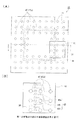
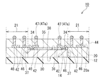
図1及び図2を参照して、この発明の第1の実施の形態の半導体装置につき説明する。図1(A)は第1の実施の形態の半導体装置の構成を説明するための上面からみた概略的な平面図であり、図1(B)は、配線パターンと電極ポストとの接続関係を説明するために、図1(A)の一部領域を拡大して示した概略的な要部平面図である。また、図2は、図1(A)のI−I破線により切断した切断面を示す概略的な断面図である。
【0036】
この発明の第1の実施の形態の半導体装置10は、下地12上に、半導体チップ30を具えている。
【0037】
下地12は、例えばガラスエポキシ、又はポリイミド等の有機材料からなる板状体又はシート状体、セラミック基板、金属基板及びSi基板等から、所望により適宜選択することができる。半導体チップの放熱効果を高めることができるので、好ましくは金属基板を選択するのがよい。
【0038】
なお、以下、半導体装置10及び半導体チップ30の形状は、直方体とした例につき説明するが、何ら直方体に限定されるものではない。
【0039】
この半導体チップ30は、所定の機能を有する回路素子(図示せず。)を具えている。半導体チップ30は第1の主表面36と、この第1の主表面36に対向する第2の主表面38を具えている。半導体チップ30は、第1の主表面36上に表面保護膜35と、この表面保護膜35の表面と第2の主表面38との間に存在する1又は2以上の側面37とを具えている。この表面保護膜35は絶縁性の材料により構成されている。回路素子に接続されている複数の電極パッド34は、第1の主表面36上に、表面保護膜35から少なくともその一部分が露出するように、第1の主表面36の周縁に沿って形成されている。
【0040】
そして、この半導体チップ30は、下地12上に、第1の主表面36が上面となるように、すなわち第2の主表面38が、下地12の半導体チップ配置領域14に対面するように設けられている。
【0041】
また、この発明の半導体装置10は、下地12上の半導体チップ配置領域以外の領域に、拡張部20を具えている。拡張部20は、下地12上の半導体チップ配置領域14に配置されている半導体チップ30の側面37、すなわち表面保護膜35の表面及び第2の主表面36及び38以外の面を囲むように、設けられている。このとき、半導体チップ30の表面保護膜35の表面のレベルは、拡張部20の第1の面20aのレベルと実質的に同一のレベルとなるようにされる。
【0042】
この拡張部20は、例えばエポキシ樹脂等の絶縁性の材料から適宜選択して形成することができる。また、従来適用されるいわゆる液状樹脂又はモールド樹脂を適用することができる。
【0043】
拡張部20は、製造工程において、この発明の半導体装置10に生じる反りの発生を抑制するために、好ましくは、後に形成される封止部の成形収縮よりも大きい成形収縮を有する絶縁性の材料により形成するのがよい。
【0044】
ここでいう「成形収縮」とは、成形工程において生じる材料単体での収縮を意味する。すなわち「成形収縮」とは、成形温度における硬化収縮と成形温度から常温に戻るまでの熱収縮との和に相当する(以下の説明においても同様。)。
【0045】
すなわち、拡張部20は、材料としてガラス転移点より低い温度範囲での線膨張係数が1.5×10⁻⁵/℃よりも小さく、かつ弾性率が7.8〜22GPaの範囲の絶縁性の液状樹脂により形成するのがよい。拡張部20にモールド樹脂を適用する場合については後述する。
【0046】
拡張部20の第1の面20a及び表面保護膜35上には、配線パターン42が、電極パッド34に電気的に接続されて形成されている。配線パターン42は、電極パッド34に電気的に接続されるように、電極パッド34、すなわち表面保護膜35の上側から拡張部20の上側を含む領域、すなわち拡張された領域21へと導出されるパターンを含んで形成される。
【0047】
これら配線パターン42が形成されている表面保護膜35及び拡張部20を覆うように封止部44が設けられている。配線パターン42各々からこの封止部44を貫通して、この封止部44の表面に達する電極ポスト46がそれぞれ設けられている。これら電極ポスト46の一部は、半導体チップ30の上側(真上)に設けられており、また、残りの電極ポスト46は拡張部20の上側(真上)に設けられている。通常は、これら電極ポスト46は、一定の間隔で配列させてある。また、各電極ポスト46の一部分、すなわち頂面(表面)は、封止部44の表面に露出している。この電極ポスト46はポスト電極とも称せられ、その露出された頂面には外部端子47が設けられている。外部端子47としては通常、半田ボール47aを設けている。この外部端子47は電極パッド34の配列間隔よりも広い間隔で配列されて設けられている。
【0048】
ここで、図1(B)を用いて、電極パッド34と配線パターン42との接続関係につき説明する。これらの接続関係の理解を容易にするために図1(A)の部分領域(実線で囲まれた領域)11を拡大して示してある。配線パターン42は、外部端子47の下部に接続されて位置する電極ポスト(図2に46で示す。)と、対応する電極パッド34とが規則的、かつ電気的に接続されている。これら配線パターン42を構成する配線として、例えば長配線42a、中配線42b及び短配線42cを設ける。これらの配線42a、42b及び42cを、それぞれ対応する電極パッド34に、1つの配線と1つの電極パッドという、1対1の接続関係で、接続してある。配線パターン42は、適用可能な配線プロセスルールに従って、配線幅、配線間隔及び最適角度等を決定して、可能な限り最短距離となるように電極パッド34に接続される。
【0049】
この配線パターン42は、半導体チップ30の上側(真上)の領域及び拡張部20の上側(真上)、すなわち拡張された領域21の境界にまたがるように設けられている。
【0050】
そのため、配線パターン42のうち、この境界上及び境界近傍のある程度の長さの部分領域をより太い、すなわち幅広あるいは肉厚の配線とするのがよい。
【0051】
このように、特にエッジ部効果とか、熱ストレス等により応力が集中しやすいと思われるパターン42の部分領域を太く形成しておくことにより、半導体装置10の動作の信頼性が向上する。
【0052】
この拡張部20の上側(真上)の領域は、外部端子形成領域を半導体素子の表面領域外に拡張している意味で拡張された領域21と称せられる。この構成例では拡張された領域21にも電極ポスト46が形成されている。そして、配線パターン42及び電極ポスト46を覆うように、封止部44を形成する。封止部44は電極ポスト46の一部分が露出するように形成されている。
【0053】
この電極ポスト46を介して、外部端子47が形成されている。電極ポストを介さずに、封止部44から配線パターン42の一部分を露出させて、直接的に配線パターン42に外部端子を接続する構成とすることもできる。
【0054】
この構成例では、外部端子47を、例えば半田ボール47aで形成している。これら半田ボール47aは、露出している電極ポスト46の頂面に設けられていて、これら電極ポスト46を介して、配線パターン42と接続されている。この隣接する電極ポスト46同士の配列及びその間隔は、例えばプリント基板等への実装を考慮して、所望の配列及び間隔とすることができる。
【0055】
既に説明したとおり、これら電極ポスト46は、半導体チップ30の上側に対応する表面積の範囲のみならず、拡張部20の上側、すなわち拡張された領域21にも設けてある。従って、電極ポスト46の配置位置及び配置間隔の設計の自由度が増す。すなわち、より実装が容易になるように、外部端子47の配置間隔の制限を緩和して、例えば実装基板側の構成上の要件に沿った、より広い間隔で形成することができる。具体的には拡張部20の面積を適宜調整することで、適切な配置間隔で、所望の数の外部電極を形成することができる。
【0056】
この発明の半導体装置10の構成によれば、半導体チップ30の真上の領域外、すなわち拡張された領域21に、外部端子47を設ける構成としてあるので、半導体装置10をいわゆるファンアウト構造又は表面保護膜35上の領域にも外部端子47が形成されているファンイン/ファンアウト構造として構成することが可能である。従って、外部端子47の配置間隔及び配置位置等の設計の自由度を大きくすることができる。
【0057】
また、この発明の半導体装置10は、いわゆるWCSPの製造工程を利用して、基板等のインターポーザを使用せずに半導体チップ30と外部電極47とを直接的に接続する構成とすることができるので、上述の効果に加えて、例えばワイヤボンディング接続との比較では、さらなる動作の高速化、高機能化、多機能化及びコンパクト化を図ることができる。また、例えばフリップチップ接続との比較では、同等の電気的特性を有する半導体装置10をより安価に得ることができる。
【0058】
次に図3(A)〜図9(B)を参照して、第1の実施の形態の半導体装置の製造方法につき説明する。
【0059】
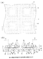
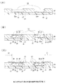
原則として、各図(A)はこの発明の半導体装置の構成を説明するための概略的な部分的平面図であり、各図の(B)は(A)図のI−I破線により切断した切断面を示す概略的な断面図である。なお、例外として、図5(B)は、図5(A)に示した、実線11で囲まれた部分を拡大して示す拡大図であり、さらに図6は、図5(A)のI−I線に沿って切断して示した断面図である。
【0060】
また、この発明の半導体装置の製造方法を説明するにあたり、各図では下地上に2(縦)×X(横;Xは2以上の正数)の格子状に複数の半導体チップを配置して、同時に複数の半導体装置10を製造する例を図示してある。しかしながら、これに限定されず、より多数の半導体チップをより多くの数からなる格子状に配列して同時に製造することもできる。
【0061】
予め、下地12上に、後の工程で複数の半導体チップ30が載置される半導体チップ領域14を設定しておく。なお、半導体チップ配置領域14の輪郭は、半導体チップ30の第2の主表面38の輪郭と実質的に一致している。隣接する半導体チップ配置領域14同士間の間隔は、互いに等間隔としておく。この間隔は、後に個片化する工程に必要なマージン面積、所望の外部端子の数に応じて形成される拡張部20の面積等を考慮して、決定される。
【0062】
まず、図3(A)及び(B)に示したように、下地12上に設定された半導体チップ配置領域14以外の領域に、半導体チップ配置領域14が露出するように、絶縁性の材料20’を設ける。この絶縁性の材料20’は、例えばエポキシ樹脂等の絶縁性の材料より適宜選択して形成することができる。また、従来適用されるいわゆる液状樹脂又はモールド樹脂を適用することができる。
【0063】
拡張部20の形成には例えば以下の方法が適用可能である。
【0064】
絶縁性の材料20’を、例えばある程度の粘度を有する絶縁性のエポキシ樹脂等とする。
【0065】
▲1▼ ディスペンス法により、半導体チップ配置領域14を露出させて、供給する。この絶縁性の材料20’を、選択された絶縁性の材料20’に最適な条件及び処理により硬化する。
【0066】
▲2▼ 精密印刷法により、半導体チップ配置領域14を露出させて、絶縁性の材料20’を供給する。この絶縁性の材料20’を、選択された絶縁性の材料20’に最適な条件及び処理により硬化する。
【0067】
▲3▼ フォトリソグラフィ法より、下地12全面に供給した後に、従来公知のマスク、露光及び現像工程により、選択された絶縁性の材料20’に最適な条件及び処理で、パターニングを行うことで、拡張部20を形成する。
【0068】
ここでいう絶縁性の材料20’とは、例えば常温で、ある程度の粘性を有するペースト状のエポキシ樹脂等の材料であり、例えば加熱、紫外線照射等の好適な処理により硬化することができる材料である。
【0069】
拡張部20は、製造工程において、半導体装置10に生じてしまう反りの発生を防止するために、好ましくは、後に形成される封止部の成形収縮よりも小さい成形収縮を有する絶縁性の材料により形成するのがよい。具体的には、拡張部20は、ガラス転移温度よりも低い温度範囲で線膨張係数が1.5×10⁻⁵/℃よりも小さく、かつ弾性率が7.8〜22GPaの範囲の液状樹脂により形成するのがよい。
【0070】
特に拡張部20にモールド樹脂を適用した場合には、厚さ方向の寸法精度を高めることができるので、より高精度に拡張部20を形成することができる。
【0071】
次いで、図4に示したように、露出している半導体チップ配置領域14上に半導体装置30を設ける。
【0072】
この半導体チップ30は、所定の機能を有する回路素子(図示せず。)を具えている。半導体チップ30は第1の主表面36と、この第1の主表面36に対向する第2の主表面38を具えている。半導体チップ30は、第1の主表面36上に表面保護膜35と、この表面保護膜35の表面と第2の主表面38との間に存在する1又は2以上の側面37とを具えている。この表面保護膜35は絶縁性の材料により構成されている。回路素子に接続されている複数の電極パッド34は、第1の主表面36上に、表面保護膜35から少なくともその一部分が露出するように、第1の主表面36の周縁に沿って形成されている。
【0073】
半導体チップ30は、第2の主表面38が下地12上の半導体チップ配置領域14に対面するように、表面保護膜35の表面及び第2の主表面38以外の面、すなわち側面37を、拡張部20が囲むように配置する。このとき、表面保護膜35の表面のレベル(高さ)d1と、硬化処理後の拡張部20の第1の面20aのレベルd2とが、実質的に同一のレベルとなるように、かつ半導体チップ30と拡張部20との間に間隙が生じないように、拡張部20の厚さを含め形成領域及び/又は半導体チップの外形サイズを調節しておく。
【0074】
好ましくは、半導体チップ配置領域14上には、何らかの接着手段を設けておくのがよい。そしてこの接着手段により半導体チップ30を半導体チップ配置領域14上に接着保持しておくのがよい。
【0075】
上述では、まず、拡張部20を絶縁性の材料20’を設けてこれを硬化処理することにより形成した後に、半導体チップ30を半導体チップ配置領域14上に設ける例を説明したが、絶縁性の材料20’、例えばある程度の粘度を有する絶縁性のエポキシ樹脂を半導体チップ配置領域14以外の領域に上述の▲1▼又は▲2▼の方法により設け、半導体チップ配置領域14上に半導体チップ30を設けた後に、絶縁性の材料20’の硬化を行って拡張部20を形成する工程としてもよい。このとき、絶縁性の材料20’は、表面保護膜35の表面のレベルと硬化後の拡張部20の第1の面20aのレベルとが実質的に同一のレベルとなるように、絶縁性の材料20’の厚さを調節すればよい。
【0076】
然る後、図5及び図6に示したように、表面保護膜35上及び拡張部20の第1の面20a上に、複数の配線パターン42を形成する。これら配線パターン42の形成は、それぞれの配線パターン42が対応する電極パッド34に電気的に接続するように設定してから、形成されるべき外部端子の配置を考慮して行う。これら複数の配線パターン42には、電極パッド34から拡張部20上、すなわち拡張された領域21へと導出されたパターンが含まれている。
【0077】
具体的には適用可能な配線プロセスルールに従って、配線幅、配線間隔及び最適角度等を決定して、可能な限り最短距離となるように接続する。例えば図示したように半導体チップ30の周縁に沿って形成されている複数の電極パッド34に対して、原則として最短距離となるように、長配線42a、中配線42b及び短配線42cを一組とする配線パターン群を複数組形成し、一方の端部をそれぞれ対応する電極パッド34に接続する。そして、他方の端部には、電極ポスト搭載用のパッドを形成して、電極ポストを介して外部端子47(半田ボール47a)を接続してある。特に長配線42a及び中配線42bは、表面保護膜35に設けられている電極パッド34から、拡張部20の上側(真上)に導出されるように設けてある。
【0078】
なお、図4(A)及び図5(A)において、説明を容易にするために、電極パッド34の配置数は、実際よりも少ない数として概略的に図示してある(以下の図においても同様。)。
【0079】
この配線パターン42の形成は、拡張部20の第1の面20aの上側(真上)の領域を含む所望の領域に、スパッタ及びフォトリソグラフィ等の従来公知のWCSPの製造工程における配線パターンの形成プロセスにより、例えば銅、アルミニウム及び金属合金等の適宜の材料を選択して、行うことができる。
【0080】
この配線パターン42の形成工程において、上述した半導体チップ30と拡張部20との間にわずかながら間隙が生じてしまう可能性もある。この配線パターン42に、このような間隙等に基因する応力が集中すると想定される場合には、この応力が集中する配線パターン42の部分を実質的に含む配線パターン42の領域を若干太く、すなわち幅広または肉厚に形成してもよい。
【0081】
次いで、図7(A)及び(B)に示したように、各配線パターン42の表面上に、これらと電気的に接続される電極ポストをそれぞれ形成する。これら電極ポスト46を拡張部20の上側(真上)の拡張された領域21と、半導体チップ30の上側(真上)の領域とに設けてある。これら電極ポスト46は、格子状に所定の間隔で配列するように形成する。この間隔は、上述したように実装を考慮した間隔、すなわち一定な、或いは不規則の間隔とすることができる。
【0082】
この電極ポスト46はメッキ及びフォトリソグラフィ等の従来公知のWCSPの製造工程における電極ポスト46の形成プロセスにより、材料を適宜選択して、行うことができる。
【0083】
さらに拡張部20の第1の面20aの上側(真上)及び半導体チップ30の上側(真上)に形成されている配線パターン42及び電極ポスト46を覆うように、封止部44を形成する。
【0084】
この封止工程は、従来公知の方法により、従来公知の封止材料、例えばエポキシ系のモールド樹脂を使用して実施することができる。
【0085】
ここで一般的に使用されるモールド樹脂としては、例えば線膨張係数が0.6〜1.3×10⁻⁵/℃の範囲であり、ガラス転移温度(Tg)が125〜220℃の範囲であり、弾性率が9.8〜24GPa(1000〜2450kg/mm2)の範囲の物性値を有するものが挙げられる。
【0086】
製造工程における半導体装置10の反りの発生を防止するために、特に拡張部20を、封止部44と同様にいわゆるモールド樹脂で形成する場合には、成形収縮が封止部44よりも大きくなるように決定される。例えば、拡張部20及び封止部44を形成するモールド樹脂の物性について、以下の組み合わせが挙げられる。
【0087】
▲1▼ 拡張部/封止部:拡張部のモールド樹脂の物性は、ガラス転移温度よりも低い温度範囲での線膨張係数が1.1〜1.5×10−5/℃の範囲であって、かつガラス転移温度(Tg)が170℃よりも大きい/封止部のモールド樹脂の物性は、ガラス転移温度よりも低い温度範囲での線膨張係数が1.0×10−5/℃より小さく、ガラス転移温度(Tg)が125〜220℃の範囲であり、かつ弾性率が14.7〜24GPa(1500〜2450kg/mm2)の範囲。
【0088】
▲2▼ 拡張部/封止部:拡張部のモールド樹脂の物性は、ガラス転移温度よりも低い温度範囲での線膨張係数が1.1〜1.7×10−5/℃の範囲であって、かつガラス転移温度(Tg)が170℃よりも小さく、弾性率が9.8〜19.6GPa(1000〜2000kg/mm2)/封止部のモールド樹脂の物性は、ガラス転移温度よりも低い温度範囲での線膨張係数が1.0×10−5/℃より小さく、ガラス転移温度(Tg)が125〜220℃の範囲であり、弾性率が14.7〜24GPa(1500〜2450kg/mm2)の範囲。
【0089】
▲3▼ 拡張部/封止部:拡張部のモールド樹脂の物性は、ガラス転移温度よりも低い温度範囲での線膨張係数が1.1〜1.7×10−5/℃の範囲であり、かつ弾性率が13.7GPa(1400kg/mm2)であり、かつガラス転移温度(Tg)が125℃〜170℃の範囲/封止部のモールド樹脂の物性は、ガラス転移温度よりも低い温度範囲での線膨張係数が1.0×10−5/℃より小さく、ガラス転移温度(Tg)が125〜220℃の範囲であり、かつ弾性率が14.7〜24GPa(1500〜2450kg/mm2)の範囲。
【0090】
然る後、図8(A)及び(B)に示したように、封止部44をその表面側から削り取って、電極ポスト46の頂面(上面とも称する。)の一部分を、露出させる。
【0091】
この工程は、従来公知の研削や、研磨工程を適用して行う。
【0092】
また、封止部44の形成に、フィルム成形等の方法を適用することもできる。その場合には、電極ポスト46に実質的に負荷をかけることがない。また、その場合には、上述した封止部44に対する研削工程を要せずに電極ポスト46の頂面を封止部44の表面に露出するように直接的に形成する。
【0093】
このとき、露出した電極ポスト46の上面に、選択される材料により何らかの処理を行ってもよい。例えば材料を銅とした場合にはバリアメタル層として薄いNi(ニッケル)膜等を形成してもよい。
【0094】
次いで、封止部44の表面から露出している電極ポスト46を介して電極ポスト46の上面に、外部端子47として例えば半田ボール47aを、形成する。
【0095】
次いで、図9(A)及び(B)に示したように、一点破線aで示した切断線に沿って、複数の半導体チップ同士の間を切断して、半導体チップを含む半導体装置として個片化する。
【0096】
この個片化工程は、好ましくは高速回転するブレードにより、切削することにより行うのがよい。
【0097】
このように第1の実施の形態の製造方法によれば、いわゆるWCSPの製造工程を適用できるので半導体装置10を製造するための特別な工程を使用することなく半導体装置10を簡易な工程で製造することができる。
【0098】
(第2の実施の形態)
次に図10〜図12(C)を参照して、この発明の第2の実施の形態の半導体装置及びその製造方法につき説明する。なお、後述する製造工程において、適用される材料、工程の実施条件等は第1の実施の形態とほぼ同様であるので、その詳細な説明は省略する。また、各図において、平面図は第1の実施の形態で説明した図と同様であるのでその詳細な説明は省略する。
【0099】
図10を参照して、この発明の第2の実施の形態の半導体装置につき説明する。図10は第2の実施の形態の半導体装置の概略的な断面図である。
【0100】
この発明の第2の実施の形態の半導体装置10は、下地12を具えている。下地12上には、半導体チップ配置領域14が設定されている。
【0101】
そして下地12上には、絶縁性の拡張部20が形成されている。拡張部20は、半導体チップ配置領域14の輪郭と一致する底面部22aを有する凹部22を具えている。
【0102】
凹部22内には、半導体チップ30が設けられている。この半導体チップ30は、所定の機能を有する回路素子(図示せず。)を具えている。半導体チップ30は第1の主表面36と、この第1の主表面36に対向する第2の主表面38を具えている。半導体チップ30は、第1の主表面36上に表面保護膜35と、この表面保護膜35の表面と第2の主表面38との間に存在する1又は2以上の側面37とを具えている。この表面保護膜35は絶縁性の材料により構成されている。回路素子に接続されている複数の電極パッド34は、第1の主表面36上に、表面保護膜35から少なくともその一部分が露出するように、第1の主表面36の周縁に沿って形成されている。
【0103】
そして、この半導体チップ30は、第1の主表面36が上面となるように、すなわち第2の主表面38が、拡張部20の凹部22の底面部22aに対面するように設けられている。
【0104】
結果として、拡張部20は、半導体チップ30の表面保護膜35以外の面、すなわち、側面37及び第2の主表面38を囲むように、設けられている。この拡張部20は、表面保護膜35の表面のレベルと、硬化処理後の拡張部20の第1の面20aのレベルとが、実質的に同一のレベルとなるように、形成される。
【0105】
この拡張部20を形成するための材料の物性等の要件については、第1の実施の形態で既に説明したとおりであるので、その詳細な説明を省略する。
【0106】
拡張部20の第1の面20a及び表面保護膜35上には、図5で説明したのと同様に、複数の配線パターンを具えた配線パターン42が、露出している電極パッド34に電気的に接続されて形成されている。
【0107】
配線パターン42は、半導体チップ30の出力信号、半導体装置10に要求される外部端子の配置位置等を考慮して、所望のパターンで形成することができる。
【0108】
この配線パターン42は、半導体チップ30の上側(真上)の領域及び拡張部20の上側(真上)の領域の境界にまたがるように設けられている。すなわち、少なくとも複数の配線パターン42のうち一部分は、表面保護膜35から露出している電極パッド34のそれぞれと個別的に、かつ電気的に接続されて、拡張部20の上側、すなわち拡張された領域21に導出されている。
【0109】
この配線パターン42が形成されている拡張部20の第1の面20a上及び表面保護膜35上には、封止部44が、配線パターン42の一部分を露出するように形成されている。
【0110】
そして、この露出している配線パターン42上であって、拡張部20上を含む領域には、外部端子47が接続されている。
【0111】
この構成例では拡張された領域21にも例えば電極ポスト46を介して、外部端子47が形成されている。
【0112】
この構成例では、外部端子47を、例えば半田ボール47aで形成している。これら半田ボール47aは、電極ポスト46の頂面と接触して設けられていて、これら電極ポスト46を介して、配線パターン42と接続されている。この隣接する電極ポスト46同士の配列及びその間隔は、例えばプリント基板等への実装を考慮して、所望の配列及び間隔とすることができる。
【0113】
既に説明したとおり、これら電極ポスト46は、半導体チップ30の上側に対応する表面積の範囲のみならず、拡張部20の上側にも設けている。従って、電極ポスト46、すなわち外部端子47の配置位置及び配置間隔の設計の自由度が増す。すなわち、より実装が容易になるように、電極ポスト46、すなわち外部端子47の配置間隔の制限を緩和して、例えば実装基板側の構成上の要件に沿った、より広い間隔で形成することができる。具体的には拡張部20の面積を適宜調整することで、適切な配置間隔で、所望の数の外部電極を形成することができる。
【0114】
この発明の第2の実施の形態の半導体装置10は、第1の実施の形態の半導体装置の構成により得られる効果に加えて、半導体チップ30の第2の主表面38も拡張部20により覆う構成としてあるので、半導体チップ30を外部環境からより効果的に保護することができる。
【0115】
次に図11(A)〜図12(C)を参照して、第2の実施の形態の半導体装置の製造方法につき説明する。
【0116】
各図は、第2の実施の形態の半導体装置の製造方法を説明するための概略的な断面図である。
【0117】
予め、下地12上に、適用される半導体チップ30の外形サイズに合わせて半導体チップ配置領域14を設定しておく。隣接する半導体チップ配置領域14同士間の間隔は、互いに等間隔としておく。この間隔は、後に個片化する工程に必要なマージン面積、所望の外部端子の数に応じて形成される拡張部の面積等を考慮して、決定される。
【0118】
まず、図11(A)に示したように、この下地12上に、拡張部20を形成するための絶縁性の材料20’を設ける。ここでいう絶縁性の材料20’とは、例えば常温である程度の粘性を有するペースト状の樹脂等の材料であり、例えば加熱、紫外線照射等の好適な処理により硬化することができる材料である。例えばエポキシ樹脂等の絶縁性の材料より適宜選択することができる。また、例えばエポキシ樹脂として、従来適用されるいわゆる液状樹脂又はモールド樹脂を適用することができる。
【0119】
拡張部20の形成方法については、第1の実施の形態で説明した▲1▼ディスペンス法、▲2▼精密印刷法及び▲3▼フォトリソグラフィ法により、同様の工程で拡張部20を形成することが可能である。
【0120】
絶縁性の材料20’は、半導体チップ30を設けるための凹部22を具えるように下地12上に設けられる。この凹部22は、半導体チップ配置領域14の輪郭と一致する底面部22aを具えるように形成される。この凹部22の底面部22a側の厚さd3は、例えば後に設けられる半導体チップの放熱性等を考慮して、適宜設定することができる。
【0121】
まず、絶縁性の材料20’として、例えばある程度の粘度を有する絶縁性のエポキシ樹脂を、下地12上の全面に凹部22の底面部22a側の厚さd3に等しい厚さで、上述のディスペンス方式、精密印刷方式等の方法により設ける。
【0122】
次いで、これらのうちいずれかの方法で、例えば硬化処理後に、後に設けられる半導体チップの厚さd1と等しくなるように、半導体チップ配置領域14に相当する領域以外の領域に、さらに絶縁性の材料20’を設けて、凹部22を形成するように2段階の工程により、拡張部20を、形成する。
【0123】
また、例えばフォトリソグラフィ法によるパターニングを行うこともできる。すなわち、凹部22の底面部22aの厚さd3と、例えば硬化処理後に半導体チップ30の厚さd1との和d2(=d1+d3)に等しい厚さとなるように、下地12上全面に絶縁性の材料20’を設ける。次いで、下地12の半導体チップ配置領域14に相当する領域を、設定された底面部22aの側の厚さd3だけ残るように、すなわち半導体チップ30の厚さd1の分だけ、マスク、露光及び現像等の従来公知の工程により除去することで、凹部22を具えた絶縁性の材料20’のパターンを下地12上に形成する。
【0124】
この絶縁性の材料20’のパターニングは、1段階の工程で行うこともできる。例えばディスペンス方式により、凹部22の底面部を形成する際には、絶縁性の材料20’の下地12上への吐出量を減少させるように調節することで形成する。
【0125】
例えば印刷方式を適用する場合にも、マスクと下地12との間の距離を調整しつつ、設ける絶縁性の材料20’の量を調整することで、1段階の工程によりパターニングを行うことができる。
【0126】
次に、図11(B)に示したように、パターニングされた絶縁性の材料20’の凹部22に半導体チップ30を設ける。
【0127】
この半導体チップ30は、所定の機能を有する回路素子(図示せず。)を具えている。半導体チップ30は第1の主表面36と、この第1の主表面36に対向する第2の主表面38を具えている。半導体チップ30は、第1の主表面36上に表面保護膜35と、この表面保護膜35の表面と第2の主表面38との間に存在する1又は2以上の側面37とを具えている。この表面保護膜35は絶縁性の材料により構成されている。回路素子に接続されている複数の電極パッド34は、第1の主表面36上に、表面保護膜35から少なくともその一部分が露出するように、第1の主表面36の周縁に沿って形成されている。
【0128】
半導体チップ30は、第2の主表面38が、凹部22の底面部22aに対面するように、設けられている。半導体チップ30は、凹部22の底面部22aの絶縁性の材料20’の粘性により保持される。
【0129】
ここで、選択された絶縁性の材料20’に好適な条件で、例えば加熱、紫外線照射等の硬化処理することで、拡張部20を形成する。このとき、半導体チップ30の第2の主表面38に接している凹部22の底面部22aの絶縁性の材料20’も硬化される。このように半導体チップ30は、底面部22aを介して、下地12上に、接着保持される。
【0130】
半導体チップ30は、表面保護膜35以外の面、すなわち側面37及び第2の主表面38が拡張部20により、囲まれる。
【0131】
このとき、表面保護膜35の表面のレベルと、硬化処理後の拡張部20の第1の面20aのレベルとは、実質的に同一のレベルとなるようにされる。
【0132】
この例では、絶縁性の材料20’の硬化処理前に半導体チップ30を凹部内に設け、しかる後に硬化処理を行う例を説明したが、例えば上述のフォトリソグラフィ法等により、半導体チップ30を凹部22に設ける前に、絶縁性の材料20’により形成されたパターンを硬化処理して拡張部20を形成することもできる。この場合には、形成された拡張部20の凹部22内に半導体チップ30を設ける。
【0133】
このとき、好ましくは、凹部22の底面部22aに何らかの接着手段を設けておくのがよい。そして、この接着手段により半導体チップ30を凹部22に接着保持するのがよい。
【0134】
然る後、図11(C)に示したように、表面保護膜35の上側(真上)及び拡張部20の第1の面20aの上側(真上)、すなわち拡張された領域21に、複数の配線パターンを含む配線パターン42を形成する。
【0135】
この配線パターン42は、表面保護膜35の上側(真上)から拡張部20の第1の面20aの上側(真上)の領域を含む領域に、導出されるようにスパッタ及びフォトリソグラフィ等の従来公知のWCSPの製造工程における配線パターンの形成プロセスにより、例えばアルミニウム、銅及び金属合金等の適宜の材料を選択して、行うことができる。
【0136】
次いで、図12(A)に示したように、配線パターン42の表面上であって、拡張部20上に相当する領域、すなわち拡張された領域21を含む領域に、複数の電極ポスト46を、例えば格子状に所定の間隔で形成する。この複数の電極ポスト46同士の間隔は、上述したように実装を考慮した間隔として、すなわち一定な、或いは不規則の間隔とすることができる。
【0137】
この電極ポスト46はメッキ及びフォトリソグラフィ等の従来公知のWCSPの製造工程における電極ポスト46の形成プロセスにより、適宜の材料を選択して、行うことができる。
【0138】
さらに拡張部20及び/又は半導体チップ30上に形成されている配線パターン42及び電極ポスト46を覆うように、封止部44を形成する。
【0139】
この封止部44の形成工程は、従来公知の封止工程により、従来公知の封止材料、例えばエポキシ系のモールド樹脂を使用して実施することができる。
【0140】
適用されるモールド樹脂の物性等の要件については、第1の実施の形態と同様であるのでその詳細な説明は省略する。
【0141】
拡張部20及び封止部44のモールド樹脂の物性の組み合わせ例についても第1の実施の形態と同様であるので、ここでは説明を省略する。
【0142】
然る後、図12(B)に示したように、封止部44をその表面側から削り取って、電極ポスト46の頂面(上面とも称する。)を、露出させる。
【0143】
この工程は、従来公知の研削や、研磨工程を適用して行う。
【0144】
そして、封止部44の表面から露出している電極ポスト46を介してその上面に、外部端子47として例えば半田ボール47aを形成する。
【0145】
次いで、図12(C)に示したように、隣接する半導体チップ同士の間を切断して、半導体チップを含む半導体装置として個片化する。
【0146】
この個片化工程は、好ましくは高速回転するブレードにより、切削することにより行うのがよい。
【0147】
このように第2の実施の形態の製造方法によれば、特に半導体チップ30の第2の主表面38側が、拡張部20により効果的に保護されている半導体装置10を簡易な工程で製造することができる。
【0148】
(第3の実施の形態)
次に図13(A)〜(D)を参照して、この発明の第3の実施の形態の半導体装置につき説明する。この第3の実施の形態の半導体装置10は、上述の第1及び第2の実施の形態の半導体装置10の構成に加えて、拡張部20の第1の面20a及び半導体チップ30の表面保護膜35上に、絶縁膜40が形成されていることを特徴としている。また、拡張部20が、半導体チップ30側に、向かうほど徐々に薄くなっていく形状の傾斜を有する内側壁24を具えることを特徴としている。
【0149】
なお、後述する製造工程において、適用される材料、工程の実施条件等は、既に説明した第1の実施の形態とほぼ同様であるので、その詳細な説明は省略する。また、各図において、平面図についても、第1の実施の形態で既に説明した図と同様であるのでその図示及び詳細な説明は省略する。
【0150】
図13(A)、(B)、(C)及び(D)を参照して、この発明の第3の実施の形態の半導体装置につき説明する。図13(A)、(B)、(C)及び(D)は第3の実施の形態の半導体装置の概略的な断面図である。図13(A)は、第1の実施の形態の半導体装置に絶縁膜40を設けた構成例である。図13(B)は、図13(A)の変形例であって、拡張部20が半導体チップ30側に向かうほど徐々に肉薄となっていく形状の傾斜を有する内側壁24を具える構成例である。図13(C)は、第2の実施の形態の半導体チップに絶縁膜40を設けた構成例である。図13(D)は、図13(C)の変形例であって、拡張部20が、半導体チップ30側に向かうほど徐々に肉薄となっていく形状の傾斜を有する内側壁24を具える構成例である。
【0151】
この発明の第3の実施の形態の半導体装置10は、いずれも下地12を具えている。
【0152】
そして、下地12上の半導体チップ配置領域14には、拡張部20が形成されている。図13(A)及び(B)の構成例では、半導体チップ配置領域14が露出するように拡張部20が設けられている。図13(C)及び(D)の構成例の場合には、拡張部20は、後に半導体チップが設けられる凹部22を具えている。凹部22は、半導体チップ配置領域14の輪郭と一致する底面部22aを具えている。
【0153】
そして、半導体チップ配置領域14上又は凹部22内には半導体チップ30が設けられている。
【0154】
この半導体チップ30は、上述したように、所定の機能を有する回路素子(図示せず。)を具えている。半導体チップ30は第1の主表面36と、この第1の主表面36に対向する第2の主表面38を具えている。半導体チップ30は、第1の主表面36上に表面保護膜35と、この表面保護膜35の表面と第2の主表面38との間に存在する1又は2以上の側面37とを具えている。この表面保護膜35は絶縁性の材料により構成されている。回路素子に接続されている複数の電極パッド34は、第1の主表面36上に、表面保護膜35から少なくともその一部分が露出するように、第1の主表面36の周縁に沿って形成されている。
【0155】
そして、この半導体チップ30は、第1の主表面36が上面となるように、すなわち第2の主表面38が、半導体チップ配置領域14上又は拡張部20の凹部22の底面部22aに対面するように設けられている。
【0156】
結果として、拡張部20は、図13(A)及び(B)の構成においては、半導体チップ30の側面37を囲むように設けられている。図13(C)及び(D)の構成の場合には、拡張部20は半導体チップ30の表面保護膜35の表面以外の面、すなわち側面37及び第2の主表面38を囲むように、設けられている。このとき、表面保護膜35の表面のレベルと、硬化処理後の拡張部20の第1の面20aのレベルとは、実質的に同一のレベルとなるようにされる。
【0157】
拡張部20を形成するための材料の物性等の要件については、第1及び第2の実施の形態と同様であるのでここではその詳細な説明を省略する。
【0158】
拡張部20の第1の面20a及び半導体チップ30の表面保護膜35上には、半導体チップ30の電極パッド34が露出するように、絶縁膜40が形成されている。
【0159】
絶縁膜40上には複数の配線パターン42が形成されている。配線パターン42は、外部端子47の下部に接続されて位置する電極ポストと、対応する電極パッド34とが規則的、かつ電気的に接続されている。これら配線パターン42を構成する配線として、例えば長配線42a、中配線42b及び短配線42cを設ける。これらの配線42a、42b及び42cを、それぞれ対応する電極パッド34に、1つの配線と1つの電極パッドという、1対1の接続関係で、接続してある。
【0160】
これら複数の配線パターン42は、少なくともそのうち一部が半導体チップの上側(真上)の領域、すなわち電極パッド34に電気的に接続されて、ここから拡張部20の上側の領域へまたがるように導出されている。
【0161】
拡張部20の上側(真上)の領域は、外部端子形成領域を半導体チップ30の表面領域外に拡張している意味で拡張された領域21と称せられる。この構成例では拡張された領域21にも電極ポスト46を介して外部端子47とが形成されている。
【0162】
この構成例では、外部端子47を、例えば半田ボール47aで形成している。これら半田ボール47aは、電極ポスト46の頂面に設けられていて、これら電極ポスト46を介して、配線パターン42と電気的に接続されている。この隣接する電極ポスト46同士の配列及びその間隔は、例えばプリント基板等への実装を考慮して、所望の配列及び間隔とすることができる。
【0163】
絶縁膜40の表面上には、複数の配線パターンを具えた配線パターン42が、露出している電極パッド34に電気的に接続されて形成されている。
【0164】
配線パターン42は、半導体チップ30の出力信号、半導体装置10に要求される外部端子の配置位置等を考慮して、所望のパターンで形成することができる。
【0165】
この発明の第3の実施の形態の半導体装置10は、上述した第1の実施の形態で得られる効果に加えて、例えば拡張部20の表面と、半導体チップ30の表面とに段差が生じてしまう場合、拡張部20が半導体チップ30側に向かうほど徐々に肉薄となっていく形状の傾斜を有する内側壁24を有する場合、又は拡張部20の表面にうねりや窪みが生じてしまった場合等に、絶縁膜40用の材料により、後に配線パターンが形成できる程度に、段差、うねり及び/又は窪みの程度を緩和するか、又は絶縁膜40を平坦に形成することができる。従って、後の配線パターンの形成工程、電極ポストの形成工程をより安定した状態で行えるので、半導体装置10の信頼性を向上させる効果が得られる。
【0166】
次に図14(A)〜図15(C)を参照して、第3の実施の形態の半導体装置の製造方法につき説明する。ここでは図13(D)に示した構成例を代表として例示し、他の構成例と対比しながら説明する。
【0167】
各図は、第3の実施の形態の半導体装置の各製造工程を説明するための概略的な断面図である。
【0168】
予め、下地12上に、適用される半導体チップ30の外形サイズに合わせて半導体チップ配置領域14を設定しておく。隣接する半導体チップ領域14同士間の間隔は、互いに等間隔としておく。この間隔は、例えば後に個片化する工程に必要なマージン面積、所望の外部端子の数に応じて形成される拡張部の面積等を考慮して、決定される。
【0169】
まず、図14(A)に示したように、この下地12上に、拡張部20を形成するための絶縁性の材料20’を設ける。絶縁性の材料20’の物性等の要件については第1の実施の形態と同様であるのでその詳細な説明は省略する。
【0170】
この絶縁性の材料20’は、後の工程で半導体チップを設けるための凹部22を形成するように下地12上に設けられる。この凹部22は、半導体チップ配置領域14の輪郭と一致する底面部22aを具えるように形成される。この凹部22の底面部22a側の厚さd3は、例えば後に設けられる半導体チップ30の放熱性等を考慮して、適宜設定することができる。
【0171】
また、半導体装置10が図13(A)及び(B)に示した構成をとる場合には、下地12上の半導体チップ配置領域14が露出するように設ける。
【0172】
拡張部20の形成に適用可能な方法については、第1の実施の形態で説明したとおりであるのでその詳細な説明を省略する。
【0173】
図13(C)及び(D)に示した構成とする場合には、第1及び第2の実施の形態で説明したように、絶縁性の材料20’を、下地12上の全面に凹部22の底面部22a側の厚さd3に等しい厚さで、ディスペンス方式、精密印刷方式又はフォトリソグラフィ法等を適用して、1段階又は2段階の工程により凹部22を具えた拡張部20を形成する。
【0174】
このとき、硬化処理の硬化条件によって、拡張部20の凹部(開口部)22に半導体チップ30側に向かうほど徐々に肉薄となっていく形状の傾斜を有する内側壁24を形成することができる。例えば標準的な硬化工程によっても内側壁24を形成することができる。好ましくは、例えば初期硬化を適正な温度よりも高温で、材料の表面側のみが硬化する程度の時間で加熱を行った後、適正な温度で材料(層)の内部まで硬化することにより、傾斜を有する内側壁24を形成することができる。
【0175】
また、例えばフォトリソグラフィ法によるマスク、露光及び現像工程により、半導体チップ30に向かうほど徐々に肉薄となっていく内側壁24を形成することもできる。このフォトリソグラフィ法による傾斜を有する内側壁24の形成工程によれば、より精密に傾斜の角度を設定して形成することが容易になる。
【0176】
次に、図14(B)に示したように、傾斜を有する内側壁24の表面に沿って滑らせるようにして拡張部20の凹部22内に半導体チップ30を設ける。
【0177】
なお、図13(A)及び(C)の構成とする場合には、半導体チップ30を設けた後に、絶縁性の材料20’を硬化して、半導体チップ30を半導体素子配置領域14上又は凹部22内に設けた状態で拡張部20を形成してもよい。
【0178】
結果として、半導体チップ30は、表面保護膜35の表面以外の面、すなわち側面37及び第2の主表面38とが拡張部20により、囲まれる。図13(A)及び(C)の構成とする場合には、表面保護膜35の表面及び第2の主表面以外の面、すなわち側面37が拡張部20により囲まれる。
【0179】
このとき、好ましくは、表面保護膜35の表面のレベルと、硬化処理後の拡張部20の第1の面20aのレベルとは、実質的に同一のレベルとなるようにされる。
【0180】
次いで、表面保護膜35と拡張部20の表面20上には、絶縁膜40が形成される。
【0181】
絶縁膜40は、半導体チップ30の電極パッド34が露出するように形成される。
【0182】
このとき、一旦電極パッド34を覆うように絶縁膜40を形成した後、又は絶縁膜40の材料を設けた後に、例えばフォトリソグラフィ法等を用いて、電極パッド34を露出させる工程としてもよい。
【0183】
上述したように拡張部20の第1の面20aと、半導体チップ30の表面保護膜35との境界に段差が生じてしまう場合がある。また、拡張部20の第1の面20aにうねりや窪みが生じてしまう場合もある。これらの場合には、絶縁膜40用の材料により、後に配線パターン42が形成できる程度に、この段差の程度を緩和するか、又は絶縁膜40を平坦に形成することもできる。
【0184】
この絶縁膜40は、例えば拡張部20の材質等に応じた適宜の材料を用い、好適な方法を選択して実施すればよい。例えば、絶縁膜40の形成工程はスピンコート法、印刷法又は直接塗布プロセス等の従来公知の方法により、実施することができる。
【0185】
然る後、図14(C)に示したように、絶縁膜40の表面上に、複数の配線パターン42を形成する。
【0186】
この配線パターン42は、表面保護膜35の上側(真上)から拡張部20の第1の面20aの上側(真上)の領域を含む領域に、導出されるパターンを含むようにスパッタ及びフォトリソグラフィ等の従来公知のWCSPの製造工程における配線パターンの形成プロセスにより、例えばアルミニウム、銅及び金属合金等の適宜の材料を選択して、行うことができる。
【0187】
次いで、図15(A)に示したように、配線パターン42の表面上であって、拡張部20の上側(真上)に相当する領域、すなわち拡張された領域21を含む領域に、複数の電極ポスト46を、例えば格子状に所定の間隔で形成する。この複数の電極ポスト46同士の間隔は、上述したように実装を考慮した間隔として、すなわち一定な、或いは不規則の間隔とすることができる。
【0188】
この電極ポスト46はメッキ及びフォトリソグラフィ等の従来公知のWCSPの製造工程における電極ポスト46の形成プロセスにより、適宜の材料を選択して、行うことができる。
【0189】
さらに拡張部20及び/又は半導体チップ30上に形成されている配線パターン42及び電極ポスト46を覆うように、封止部44を形成する。
【0190】
この封止部44の形成工程は、従来公知の封止工程により、従来公知の封止材料、例えばエポキシ系のモールド樹脂を使用して実施することができる。
【0191】
適用されるモールド樹脂の物性等の要件については、第1の実施の形態と同様であるのでその詳細な説明は省略する。
【0192】
拡張部20及び封止部44のモールド樹脂の物性の組み合わせ例についても第1の実施の形態と同様であるので、ここでは説明を省略する。
【0193】
然る後、図15(B)に示したように、封止部44をその表面側から削り取って、電極ポスト46の頂面(上面とも称する。)を、露出させる。
【0194】
この工程は、従来公知の研削や、研磨工程を適用して行う。
【0195】
そして、封止部44の表面から露出している電極ポスト46を介してその上面に、外部端子47として例えば半田ボール47aを形成する。
【0196】
次いで、図15(C)に示したように、隣接する半導体チップ同士の間を切断して、所定の機能を発揮する単一の半導体装置を含む構造体として個片化する。
【0197】
この個片化工程は、好ましくは高速回転するブレードにより、切削することにより行うのがよい。
【0198】
このように第3の実施の形態の製造方法によれば、特に、半導体チップ30の第2の主表面38側が、拡張部20により効果的に保護されている半導体装置10を簡易な工程で製造することができる。
【0199】
この発明の半導体装置10を、例えば複数個積層する構成とすることもできる。この場合には、例えば従来公知の方法により拡張部20にスルーホールを形成し、積層用の端子を形成すればよい。
【0200】
この発明のすべての実施の形態において、電極ポスト46は、アルミニウム、銅等の導電性材料により形成するのがよい。好ましくは銅により形成するのがよい。このとき電極ポスト46の表面に薄い酸化層を形成しておくのがよい。このようにすれば電極ポスト46と封止部44の接着性が向上するため、耐湿性が向上する。
【0201】
さらにこの発明のすべての実施の形態において、外部端子47として半田ボール47aを電極ポスト46上に形成する、いわゆるBGA(Ball GridArray)型につき説明したが、これに限定されない。例えば、いわゆるLGA(Land Grid Array)型等の構成することもできる。
【0202】
具体的には、露出している電極ポスト46表面に直接的に半田層を形成するか、電極ポスト46表面にバリアメタル層を形成した後、このバリアメタル層上に金(Au)メッキ層を形成する。或いは電極ポスト46表面に直接的にSn(スズ)層を形成して、これを外部端子とする構成としてもよい。
【0203】
また、この発明のすべての実施の形態において、封止部の形状は、いわゆるソーカットタイプのみならず、この発明の目的を損なわない範囲で、下地及び/又は拡張部の外形と合っていなくともよい。
【0204】
【発明の効果】
この発明の半導体装置の構成によれば、搭載される半導体チップの側面部を囲むように設けられている拡張部上、すなわち拡張された領域を含む領域にも、外部端子を設けることができる、いわゆるファンアウト構造又はファンイン/ファンアウト構造が可能な構成としてあるので、外部端子の配置間隔及び配置位置等の設計の自由度を大きくすることができる。
【0205】
この発明の半導体装置は、いわゆるWCSPの製造工程を利用して、基板等のインターポーザを使用せずに直接的に半導体チップと外部電極とを接続する構成とすることができるので、上述の効果に加えて、ワイヤボンディング接続との比較では、さらなる動作の高速化、高機能化、多機能化及びコンパクト化を図ることができる。また、フリップチップ接続との比較では、同等の電気的特性をより安価に得ることができる。
【0206】
この発明の製造方法によれば、第1、第2及び第3の実施の形態の半導体装置を簡易な工程で製造することができる。特に絶縁膜を設けない構成例によれば、工程の削減による効率的な製造及びさらなるコスト削減効果が期待される。さらに半導体装置の第2の主表面に接するように、拡張部の材料を設ける例によれば、硬化により、これらを互いに接着することができるので、より容易に半導体装置を製造することができる。また、傾斜している内側壁を有する拡張部をあらかじめ構成する構成例によれば、内側壁の表面上を滑らせるようにして開口部(凹部)内に位置決めして半導体チップを効率的に設けることができるので、製造工程の効率のさらなる向上が期待される。
【図面の簡単な説明】
【図1】(A)はこの発明の半導体装置の構成を説明するための上面からみた概略的な平面図であり、(B)は、配線パターンと電極パッドとの接続関係を説明するために、(A)の一部領域を拡大して示した概略的な要部平面図である。
【図2】図1(A)のI−I破線により切断した第1の実施の形態の半導体装置の切断面を示す概略的な断面図である。
【図3】(A)及び(B)は、この発明の第1の実施の形態の半導体装置の製造方法を説明するための上面からみた概略的な平面図及び断面図(1)である。
【図4】(A)及び(B)は、この発明の第1の実施の形態の半導体装置の製造方法を説明するための上面からみた概略的な平面図及び断面図(2)である。
【図5】(A)及び(B)は、この発明の第1の実施の形態の半導体装置の製造方法を説明するための上面からみた概略的な平面図及び要部拡大平面図(3)である。
【図6】この発明の第1の実施の形態の半導体装置の製造方法を説明するための概略的な断面図(3−2)である。
【図7】(A)及び(B)は、この発明の第1の実施の形態の半導体装置の製造方法を説明するための上面からみた概略的な平面図及び断面図(4)である。
【図8】(A)及び(B)は、この発明の第1の実施の形態の半導体装置の製造方法を説明するための上面からみた概略的な平面図及び断面図(5)である。
【図9】(A)及び(B)は、この発明の第1の実施の形態の半導体装置の製造方法を説明するための上面からみた概略的な平面図及び断面図(6)である。
【図10】この発明の第2の実施の形態の半導体装置の構成を説明するための概略的な断面図である。
【図11】(A)、(B)及び(C)は、この発明の第2の実施の形態の半導体装置の製造方法を説明するための概略的な断面図(1)である。
【図12】(A)、(B)及び(C)は、この発明の第2の実施の形態の半導体装置の製造方法を説明するための概略的な断面図(2)である。
【図13】(A)、(B)、(C)及び(D)は、この発明の第3の実施の形態の半導体装置の構成例を説明するための概略的な断面図である。
【図14】(A)、(B)及び(C)は、この発明の第3の実施の形態の半導体装置の製造方法を説明するための概略的な断面図(1)である。
【図15】(A)、(B)及び(C)は、この発明の第3の実施の形態の半導体装置の製造方法を説明するための概略的な断面図(2)である。
【符号の説明】
10:半導体装置
11:部分領域
12:下地
14:半導体チップ配置領域
20:拡張部
20a:第1の面
20b:第2の面
21:拡張された領域
22:開口部(凹部)
22a:底面部
24:内側壁
30:半導体チップ
34:電極パッド
35:表面保護膜
36:第1の主表面
38:第2の主表面
40:絶縁膜
42:配線パターン
42a:長配線
42b:中配線
42c:短配線
44:封止部
46:電極ポスト
47:外部端子
47a:半田ボール[0001]
BACKGROUND OF THE INVENTION
The present invention relates to a semiconductor device and a method for manufacturing the same, and more particularly to a semiconductor device having a configuration for dealing with a further increase in external terminals and a method for manufacturing the same.
[0002]
[Prior art]
In recent years, further reduction in size and thickness of packaged semiconductor devices has been demanded. In order to meet this requirement, a package form called a wafer level chip size package (hereinafter also simply referred to as WCSP) is proposed in which the package outer size is substantially the same as the outer size of the semiconductor chip. Has been.
[0003]
The WCSP includes a semiconductor chip. The semiconductor chip includes a circuit element having a predetermined function and a plurality of electrode pads electrically connected to the circuit element. An insulating film is formed on the first main surface so as to expose the plurality of electrode pads.
[0004]
On the surface of the insulating film, a plurality of wiring patterns connected to the exposed electrode pads are formed.
[0005]
Electrode posts are formed on these wiring patterns. A sealing portion is formed so as to cover the insulating film and the wiring pattern and to expose the top surface of the electrode post.
[0006]
Furthermore, on the top surface of the electrode post, for example, in the case of a BGA package, a plurality of external terminals provided as solder balls are provided.
[0007]
As described above, the WCSP has a so-called fan-in structure in which a plurality of external electrodes are provided in a region corresponding to the circuit formation surface of a semiconductor chip, for example, in a lattice shape.
[0008]
A semiconductor chip having an electrode pad for the purpose of preventing the breakage at the connecting portion between the printed board and the external electrode when mounting the semiconductor chip having the external electrode of such a fan-in structure on the printed board. A wiring formed at a predetermined position on the semiconductor chip and connected to the electrode pad; an external electrode formed at a predetermined position on the wiring and connected to the wiring; and a printed board connected to the external electrode; A structure having a substrate formed on a semiconductor chip and having a resin layer on the substrate for matching the thermal expansion of the substrate and the printed board, in particular, an external electrode is provided on the resin layer. A known semiconductor device is known (for example, see Patent Document 1).
[0009]
[Patent Document 1]
JP 2000-208556 A (Claims and FIG. 5)
[0010]
[Problems to be solved by the invention]
As the functionality of semiconductor devices increases, the number of external terminals formed in one packaged semiconductor device tends to increase. Conventionally, such a demand for an increase in the number of external terminals is addressed by a configuration in which the interval between adjacent external terminals is narrowed. Regarding the arrangement interval and arrangement position of the external terminals, the degree of freedom of design is remarkably limited as described below.
[0011]
In the conventional WCSP described above, the minimum interval between adjacent external terminals is specifically about 0.5 mm. In the case of a 7 mm × 7 mm square WCSP, the number of external terminals provided is about 160.
[0012]
Due to the demand for further increase in external terminals of packaged semiconductor devices, it is desired to provide about 300 external terminals on a 7 mm × 7 mm square WCSP.
[0013]
In the WCSP described above, it is technically impossible to form a larger number of external electrodes on the surface of the WCSP by narrowing the interval between adjacent external terminals.
[0014]
However, it is quite difficult to form 300 external terminals on the surface area of a 7 mm × 7 mm square WCSP. Further, if the interval between the external terminals is reduced, an extremely advanced technique is required to mount the WCSP on the mounting substrate.
[0015]
For example, it may be required to form the intervals between the plurality of external terminals within a range of about 0.3 mm to 0.7 mm according to the mounting pitch of the mounting substrate.
[0016]
In such a case, in a conventional package configuration, a semiconductor chip is connected on a substrate by so-called flip chip connection, and the semiconductor chip is connected to an external electrode through the substrate or by wire bonding. The semiconductor chip is connected to the external electrode through the substrate. Since any of the connection methods uses a substrate, and an extra sealing material for the height of the wire loop is required, the package becomes thick. Furthermore, the cost of the substrate increases, and the package becomes expensive. In particular, in the case of flip chip connection, a more expensive build-up substrate is required, so that the package becomes more expensive.
[0017]
On the other hand, when the connection by wire bonding is performed, the inductance of the wire portion is increased.
[0018]
SUMMARY OF THE INVENTION Accordingly, an object of the present invention is to provide a semiconductor device having a configuration capable of increasing the degree of freedom in designing the arrangement intervals and arrangement positions of external terminals and making the package itself compact.
[0019]
[Means for Solving the Problems]
In order to achieve this object, the semiconductor device of the present invention has the following structural features. That is, the semiconductor device according to the present invention is formed so that the base, the first main surface provided with the plurality of electrode pads provided on the base, and the electrode pads exposed on the first main surface. And a semiconductor chip having a second main surface opposite to the first main surface, and a plurality of side surfaces between the surface of the surface protective film and the second main surface. Yes.
[0020]
An insulating extension is formed so as to surround the side surface of the semiconductor chip.
[0021]
A plurality of wiring patterns are electrically connected to each electrode pad and led out from the electrode pad onto the surface of the extension.
[0022]
A sealing portion is formed on the wiring pattern so as to expose a part of the wiring pattern.
[0023]
A plurality of external terminals are provided on the wiring pattern in a region including the upper side of the extended portion.
[0024]
According to the configuration of the semiconductor device of the present invention, since the external electrode can be provided also in the region including the extended portion provided so as to surround the semiconductor chip, the arrangement interval and the arrangement position of the external electrode It is possible to provide a semiconductor device having an increased degree of design freedom. In addition, since the semiconductor device of the present invention can be configured not to use an interposer such as a substrate by applying a so-called WCSP manufacturing process, the operation speed can be further increased compared with the wire bonding connection. Functionalization, multifunctionalization, and compactness can be achieved. Further, in comparison with flip-chip connection, equivalent electrical characteristics can be obtained at a lower cost.
[0025]
The main steps of the semiconductor device manufacturing method of the present invention are as follows.
[0026]
(1) A plurality of semiconductor chip placement areas in which a plurality of semiconductor chips are placed are set on a base at predetermined intervals.
[0027]
(2) The extended portion is formed of an insulating material in a region other than the semiconductor chip arrangement region on the base.
[0028]
(3) A first main surface having a plurality of electrode pads on the semiconductor chip arrangement region, a surface protective film formed so as to expose the electrode pads on the first main surface, and a first A semiconductor chip having a second main surface facing the main surface of the semiconductor chip and a plurality of side surfaces between the surface of the surface protective film and the second main surface, and the second main surface and the semiconductor chip arrangement region are Provide to face each other.
[0029]
(4) A wiring pattern led out from the electrode pad to a region including on the extended portion is formed.
[0030]
(5) A sealing portion is formed on the wiring pattern so as to expose a part of the wiring pattern in a region including the extension portion.
[0031]
(6) A plurality of external terminals are formed on the wiring pattern in the region including the extension portion.
[0032]
(7) A plurality of semiconductor chips are cut to singulate a semiconductor device including the semiconductor chips.
[0033]
According to the method for manufacturing a semiconductor device of the present invention, it is possible to provide a highly functional, multi-functional and compact semiconductor device by a simpler process. In particular, the degree of freedom in designing the arrangement interval and arrangement position of the external electrodes can be greatly increased.
[0034]
DETAILED DESCRIPTION OF THE INVENTION
Hereinafter, embodiments of the present invention will be described with reference to the drawings. In the drawings, only the shapes, sizes, and arrangement relationships of the respective constituent components are schematically shown to such an extent that the present invention can be understood, and the present invention is not particularly limited thereby. In the following description, specific materials, conditions, numerical conditions, and the like may be used. However, these are merely preferred examples, and are not limited to these. In addition, it should be understood that the same constituent components are denoted by the same reference numerals in the drawings used for the following description, and redundant description thereof may be omitted.
[0035]
(First embodiment)
A semiconductor device according to a first embodiment of the present invention will be described with reference to FIGS. FIG. 1A is a schematic plan view seen from the upper surface for explaining the configuration of the semiconductor device of the first embodiment, and FIG. 1B shows the connection relationship between the wiring pattern and the electrode post. FIG. 2 is a schematic plan view of an essential part showing a part of the area of FIG. FIG. 2 is a schematic cross-sectional view showing a cut surface taken along a broken line II in FIG.
[0036]
The
[0037]
The base 12 can be appropriately selected as desired from, for example, a plate-like body or a sheet-like body made of an organic material such as glass epoxy or polyimide, a ceramic substrate, a metal substrate, and a Si substrate. Since the heat dissipation effect of the semiconductor chip can be enhanced, it is preferable to select a metal substrate.
[0038]
In addition, although the shape of the
[0039]
The
[0040]
The
[0041]
In addition, the
[0042]
The
[0043]
In order to suppress the occurrence of warpage occurring in the
[0044]
Here, “molding shrinkage” means shrinkage of a single material that occurs in the molding process. That is, “molding shrinkage” corresponds to the sum of curing shrinkage at the molding temperature and heat shrinkage from the molding temperature to normal temperature (the same applies to the following description).
[0045]
That is, the expanded
[0046]
On the
[0047]
A sealing
[0048]
Here, the connection relationship between the
[0049]
The
[0050]
Therefore, in the
[0051]
As described above, the reliability of the operation of the
[0052]
The region on the upper side (directly above) of the extended
[0053]
[0054]
In this configuration example, the
[0055]
As already described, these
[0056]
According to the configuration of the
[0057]
Further, the
[0058]
Next, with reference to FIGS. 3A to 9B, a method of manufacturing the semiconductor device of the first embodiment will be described.
[0059]
In principle, each figure (A) is a schematic partial plan view for explaining the configuration of the semiconductor device of the present invention, and (B) in each figure is cut along the II broken line in FIG. It is a schematic sectional drawing which shows a cut surface. Note that, as an exception, FIG. 5B is an enlarged view showing a portion surrounded by the
[0060]
Further, in explaining the method of manufacturing a semiconductor device of the present invention, in each drawing, a plurality of semiconductor chips are arranged in a lattice pattern of 2 (vertical) × X (horizontal; X is a positive number of 2 or more) on the base. An example in which a plurality of
[0061]
A
[0062]
First, as shown in FIGS. 3A and 3B, the insulating
[0063]
For example, the following method can be applied to form the extended
[0064]
The insulating
[0065]
(1) The semiconductor
[0066]
(2) An insulating
[0067]
(3) After supplying the entire surface of the base 12 by photolithography, patterning is performed under conditions and processing optimum for the selected insulating
[0068]
The insulating
[0069]
In order to prevent the warpage that may occur in the
[0070]
In particular, when a mold resin is applied to the extended
[0071]
Next, as shown in FIG. 4, the
[0072]
The
[0073]
The
[0074]
Preferably, some bonding means is provided on the semiconductor
[0075]
In the above description, the example in which the
[0076]
Thereafter, as shown in FIGS. 5 and 6, a plurality of
[0077]
Specifically, according to the applicable wiring process rule, the wiring width, the wiring interval, the optimum angle, etc. are determined, and the connection is made so as to have the shortest possible distance. For example, as shown in the figure, a set of
[0078]
4A and 5A, for ease of explanation, the number of
[0079]
The
[0080]
In the process of forming the
[0081]
Next, as shown in FIGS. 7A and 7B, electrode posts electrically connected to these are formed on the surface of each
[0082]
The
[0083]
Further, the sealing
[0084]
This sealing step can be performed by a conventionally known method using a conventionally known sealing material, for example, an epoxy mold resin.
[0085]
As a mold resin generally used here, for example, the linear expansion coefficient is in the range of 0.6 to 1.3 × 10 −5 / ° C., and the glass transition temperature (Tg) is in the range of 125 to 220 ° C. Yes, and those having a physical property value in a range of 9.8 to 24 GPa (1000 to 2450 kg / mm 2 ).
[0086]
In order to prevent the warpage of the
[0087]
(1) Expansion part / sealing part: The physical properties of the mold resin in the expansion part are such that the linear expansion coefficient in the temperature range lower than the glass transition temperature is in the range of 1.1 to 1.5 × 10 −5 / ° C. In addition, the glass transition temperature (Tg) is larger than 170 ° C./The physical properties of the molding resin in the sealing portion are such that the linear expansion coefficient in a temperature range lower than the glass transition temperature is 1.0 × 10 −5 / ° C. The glass transition temperature (Tg) is in the range of 125 to 220 ° C. and the elastic modulus is in the range of 14.7 to 24 GPa (1500 to 2450 kg / mm 2 ).
[0088]
(2) Expansion part / sealing part: The physical properties of the mold resin in the expansion part are such that the linear expansion coefficient in the temperature range lower than the glass transition temperature is in the range of 1.1 to 1.7 × 10 −5 / ° C. In addition, the glass transition temperature (Tg) is smaller than 170 ° C., the elastic modulus is 9.8 to 19.6 GPa (1000 to 2000 kg / mm 2 ) / the physical properties of the molding resin of the sealing portion are higher than the glass transition temperature. The linear expansion coefficient in a low temperature range is smaller than 1.0 × 10 −5 / ° C., the glass transition temperature (Tg) is in the range of 125 to 220 ° C., and the elastic modulus is 14.7 to 24 GPa (1500 to 2450 kg / mm 2 ) range.
[0089]
(3) Expansion part / sealing part: The physical property of the mold resin in the expansion part is such that the linear expansion coefficient in the temperature range lower than the glass transition temperature is in the range of 1.1 to 1.7 × 10 −5 / ° C. In addition, the elastic modulus is 13.7 GPa (1400 kg / mm 2 ), and the glass transition temperature (Tg) is in the range of 125 ° C. to 170 ° C./The physical properties of the molding resin in the sealing portion are lower than the glass transition temperature. The linear expansion coefficient in the range is smaller than 1.0 × 10 −5 / ° C., the glass transition temperature (Tg) is in the range of 125 to 220 ° C., and the elastic modulus is 14.7 to 24 GPa (1500 to 2450 kg / mm). 2 ) Range.
[0090]
Thereafter, as shown in FIGS. 8A and 8B, the sealing
[0091]
This step is performed by applying a conventionally known grinding or polishing step.
[0092]
A method such as film forming can also be applied to the formation of the sealing
[0093]
At this time, the upper surface of the exposed
[0094]
Next, for example,
[0095]
Next, as shown in FIGS. 9A and 9B, a plurality of semiconductor chips are cut along a cutting line indicated by a one-dot broken line a to obtain a semiconductor device including the semiconductor chips. Turn into.
[0096]
This singulation process is preferably performed by cutting with a blade rotating at high speed.
[0097]
As described above, according to the manufacturing method of the first embodiment, since the so-called WCSP manufacturing process can be applied, the
[0098]
(Second Embodiment)
Next, a semiconductor device and a manufacturing method thereof according to the second embodiment of the present invention will be described with reference to FIGS. Note that, in the manufacturing process described later, applied materials, execution conditions of the process, and the like are substantially the same as those in the first embodiment, and thus detailed description thereof is omitted. Moreover, in each figure, since the top view is the same as the figure demonstrated in 1st Embodiment, the detailed description is abbreviate | omitted.
[0099]
A semiconductor device according to the second embodiment of the present invention will be described with reference to FIG. FIG. 10 is a schematic cross-sectional view of the semiconductor device according to the second embodiment.
[0100]
The
[0101]
An insulating
[0102]
A
[0103]
The
[0104]
As a result, the
[0105]
Since requirements such as physical properties of the material for forming the
[0106]
On the
[0107]
The
[0108]
The
[0109]
On the
[0110]
An
[0111]
In this configuration example, an
[0112]
In this configuration example, the
[0113]
As already described, these
[0114]
In the
[0115]
Next, with reference to FIGS. 11A to 12C, description will be made on a semiconductor device manufacturing method according to the second embodiment.
[0116]
Each drawing is a schematic cross-sectional view for explaining the method for manufacturing the semiconductor device of the second embodiment.
[0117]
The semiconductor
[0118]
First, as shown in FIG. 11A, an insulating
[0119]
As for the method of forming the
[0120]
The insulating
[0121]
First, as the insulating
[0122]
Next, by any of these methods, for example, after the curing process, an insulating material is further formed in a region other than the region corresponding to the semiconductor
[0123]
Further, for example, patterning by photolithography can be performed. That is, an insulating material is formed on the entire surface of the base 12 so that the thickness d3 of the
[0124]
The patterning of the insulating
[0125]
For example, even when a printing method is applied, patterning can be performed in a single step by adjusting the amount of the insulating
[0126]
Next, as shown in FIG. 11B, the
[0127]
The
[0128]
The
[0129]
Here, the
[0130]
In the
[0131]
At this time, the surface level of the surface
[0132]
In this example, the
[0133]
At this time, it is preferable to provide some bonding means on the
[0134]
Thereafter, as shown in FIG. 11C, the upper side (directly above) the surface
[0135]
This
[0136]
Next, as shown in FIG. 12A, a plurality of
[0137]
The
[0138]
Further, the sealing
[0139]
The formation process of this sealing
[0140]
Since requirements such as physical properties of the applied mold resin are the same as those in the first embodiment, detailed description thereof is omitted.
[0141]
An example of the combination of the physical properties of the mold resin of the extended
[0142]
Thereafter, as shown in FIG. 12B, the sealing
[0143]
This step is performed by applying a conventionally known grinding or polishing step.
[0144]
Then, for example,
[0145]
Next, as shown in FIG. 12C, the adjacent semiconductor chips are cut and separated into individual semiconductor devices including the semiconductor chips.
[0146]
This singulation process is preferably performed by cutting with a blade rotating at high speed.
[0147]
As described above, according to the manufacturing method of the second embodiment, the
[0148]
(Third embodiment)
Next, with reference to FIGS. 13A to 13D, a semiconductor device according to a third embodiment of the present invention will be described. In the
[0149]
Note that, in the manufacturing process described later, applied materials, process execution conditions, and the like are substantially the same as those of the first embodiment described above, and thus detailed description thereof is omitted. In each figure, the plan view is also the same as the figure already described in the first embodiment, and the illustration and detailed description thereof are omitted.
[0150]
A semiconductor device according to a third embodiment of the present invention will be described with reference to FIGS. 13 (A), (B), (C) and (D). FIGS. 13A, 13B, 13C, and 13D are schematic cross-sectional views of the semiconductor device of the third embodiment. FIG. 13A shows a configuration example in which an insulating
[0151]
Each of the
[0152]
An
[0153]
A
[0154]
As described above, the
[0155]
The
[0156]
As a result, the
[0157]
Since requirements such as physical properties of the material for forming the
[0158]
An insulating
[0159]
A plurality of
[0160]
The plurality of
[0161]
The region on the upper side (directly above) of the extended
[0162]
In this configuration example, the
[0163]
A
[0164]
The
[0165]
In the
[0166]
Next, with reference to FIGS. 14A to 15C, description will be made on a semiconductor device manufacturing method according to the third embodiment. Here, the configuration example illustrated in FIG. 13D is illustrated as a representative example, and will be described in comparison with other configuration examples.
[0167]
Each drawing is a schematic cross-sectional view for explaining each manufacturing process of the semiconductor device according to the third embodiment.
[0168]
The semiconductor
[0169]
First, as shown in FIG. 14A, an insulating
[0170]
This insulating
[0171]
When the
[0172]
Since a method applicable to the formation of the extended
[0173]
In the case of the configuration shown in FIGS. 13C and 13D, as described in the first and second embodiments, the insulating
[0174]
At this time, depending on the curing conditions of the curing process, it is possible to form the
[0175]
Further, the
[0176]
Next, as shown in FIG. 14B, the
[0177]
13A and 13C, after the
[0178]
As a result, in the
[0179]
At this time, preferably, the level of the surface of the surface
[0180]
Next, an insulating
[0181]
The insulating
[0182]
At this time, after the insulating
[0183]
As described above, there may be a step at the boundary between the
[0184]
The insulating
[0185]
Thereafter, as shown in FIG. 14C, a plurality of
[0186]
This
[0187]
Next, as shown in FIG. 15A, a plurality of regions on the surface of the
[0188]
The
[0189]
Further, the sealing
[0190]
The formation process of this sealing
[0191]
Since requirements such as physical properties of the applied mold resin are the same as those in the first embodiment, detailed description thereof is omitted.
[0192]
An example of the combination of the physical properties of the mold resin of the extended
[0193]
Thereafter, as shown in FIG. 15B, the sealing
[0194]
This step is performed by applying a conventionally known grinding or polishing step.
[0195]
Then, for example,
[0196]
Next, as shown in FIG. 15C, adjacent semiconductor chips are cut to form a structure including a single semiconductor device that exhibits a predetermined function.
[0197]
This singulation process is preferably performed by cutting with a blade rotating at high speed.
[0198]
As described above, according to the manufacturing method of the third embodiment, in particular, the
[0199]
For example, a plurality of
[0200]
In all the embodiments of the present invention, the
[0201]
Furthermore, in all the embodiments of the present invention, the so-called BGA (Ball Grid Array) type in which the
[0202]
Specifically, a solder layer is directly formed on the exposed
[0203]
Further, in all the embodiments of the present invention, the shape of the sealing portion is not limited to the so-called saw cut type, and may not match the outer shape of the base and / or the extended portion as long as the object of the present invention is not impaired. Good.
[0204]
【The invention's effect】
According to the configuration of the semiconductor device of the present invention, the external terminal can be provided on the extended portion provided so as to surround the side surface portion of the semiconductor chip to be mounted, that is, in the region including the expanded region. Since the so-called fan-out structure or fan-in / fan-out structure is possible, it is possible to increase the degree of freedom in designing the arrangement intervals and arrangement positions of the external terminals.
[0205]
The semiconductor device according to the present invention can be configured to directly connect the semiconductor chip and the external electrode without using an interposer such as a substrate by utilizing a so-called WCSP manufacturing process. In addition, in comparison with wire bonding connection, it is possible to further increase the operation speed, increase the function, increase the number of functions, and reduce the size. Further, in comparison with flip-chip connection, equivalent electrical characteristics can be obtained at a lower cost.
[0206]
According to the manufacturing method of the present invention, the semiconductor devices of the first, second and third embodiments can be manufactured by a simple process. In particular, according to the configuration example in which the insulating film is not provided, an efficient manufacturing and a further cost reduction effect due to the reduction of the process are expected. Furthermore, according to the example in which the material of the extension portion is provided so as to be in contact with the second main surface of the semiconductor device, these can be bonded to each other by curing, so that the semiconductor device can be manufactured more easily. Further, according to the configuration example in which the extended portion having the inclined inner wall is configured in advance, the semiconductor chip is efficiently provided by positioning in the opening (recess) so as to slide on the surface of the inner wall. Therefore, further improvement in the efficiency of the manufacturing process is expected.
[Brief description of the drawings]
FIG. 1A is a schematic plan view seen from the upper surface for explaining the configuration of a semiconductor device of the present invention, and FIG. 1B is a diagram for explaining a connection relationship between a wiring pattern and electrode pads. It is the schematic principal part top view which expanded and showed the partial area | region of (A).
FIG. 2 is a schematic cross-sectional view showing a cut surface of the semiconductor device of the first embodiment taken along the II broken line in FIG.
FIGS. 3A and 3B are a schematic plan view and a cross-sectional view (1) as viewed from the top for explaining the method for manufacturing a semiconductor device according to the first embodiment of the present invention; FIGS.
FIGS. 4A and 4B are a schematic plan view and a cross-sectional view (2) as viewed from the top for explaining the method for manufacturing a semiconductor device according to the first embodiment of the present invention; FIGS.
FIGS. 5A and 5B are a schematic plan view and an enlarged plan view of a main part as viewed from the top for explaining the method for manufacturing a semiconductor device according to the first embodiment of the present invention; FIGS. It is.
FIG. 6 is a schematic cross sectional view (3-2) for illustrating the method for manufacturing the semiconductor device according to the first embodiment of the present invention;
FIGS. 7A and 7B are a schematic plan view and a cross-sectional view (4) seen from the top for explaining the method for manufacturing a semiconductor device according to the first embodiment of the present invention; FIGS.
FIGS. 8A and 8B are a schematic plan view and a cross-sectional view (5) as viewed from the top for explaining the method for manufacturing a semiconductor device according to the first embodiment of the present invention; FIGS.
FIGS. 9A and 9B are a schematic plan view and a cross-sectional view (6) seen from the top for explaining the method for manufacturing a semiconductor device according to the first embodiment of the present invention; FIGS.
FIG. 10 is a schematic cross sectional view for illustrating a configuration of a semiconductor device according to a second embodiment of the present invention.
FIGS. 11A, 11B, and 11C are schematic cross-sectional views (1) for explaining the method for manufacturing the semiconductor device according to the second embodiment of the invention; FIGS.
FIGS. 12A, 12B, and 12C are schematic cross-sectional views (2) for explaining the method of manufacturing the semiconductor device according to the second embodiment of the invention; FIGS.
FIGS. 13A, 13B, and 13D are schematic cross-sectional views for explaining a configuration example of a semiconductor device according to a third embodiment of the present invention;
FIGS. 14A, 14B, and 14C are schematic cross-sectional views (1) for explaining the method of manufacturing the semiconductor device according to the third embodiment of the invention; FIGS.
FIGS. 15A, 15B, and 15C are schematic cross-sectional views (2) for explaining the method of manufacturing the semiconductor device according to the third embodiment of the invention; FIGS.
[Explanation of symbols]
10: Semiconductor device 11: Partial region 12: Base 14: Semiconductor chip placement region 20: Expanded
22a: bottom 24: inner side wall 30: semiconductor chip 34: electrode pad 35: surface protective film 36: first main surface 38: second main surface 40: insulating film 42:
Claims (23)
前記下地上に設けられている、複数の電極パッドを具えている第1の主表面と、該第1の主表面上に前記電極パッドが露出するように形成されている表面保護膜と、前記第1の主表面と対向する第2の主表面と、前記表面保護膜の表面と第2の主表面との間の複数の側面とを有する半導体チップと、
前記半導体チップの前記側面を囲むように形成されている絶縁性の拡張部と、
前記電極パッドの各々に電気的に接続され、前記電極パッドから前記拡張部の表面上へと導出されている、複数の配線パターンと、
前記配線パターン上に、該配線パターンの一部分を露出するように形成されている封止部と、
前記拡張部の上側を含む領域の前記配線パターン上に設けられた複数の外部端子と
を具えていることを特徴とする半導体装置。The groundwork,
A first main surface provided with a plurality of electrode pads provided on the base; a surface protection film formed so as to expose the electrode pads on the first main surface; A semiconductor chip having a second main surface facing the first main surface, and a plurality of side surfaces between the surface of the surface protective film and the second main surface;
An insulating extension formed so as to surround the side surface of the semiconductor chip;
A plurality of wiring patterns electrically connected to each of the electrode pads and led out from the electrode pads onto the surface of the extension;
A sealing portion formed on the wiring pattern so as to expose a part of the wiring pattern;
A semiconductor device comprising: a plurality of external terminals provided on the wiring pattern in a region including the upper side of the extended portion.
前記封止部は、前記電極ポストの頂面を露出するように形成されていることを特徴とする請求項1に記載の半導体装置。Comprising a plurality of electrode posts formed between the wiring pattern and the external terminals;
The semiconductor device according to claim 1, wherein the sealing portion is formed so as to expose a top surface of the electrode post.
(2)前記下地上の前記半導体チップ配置領域以外の領域に、拡張部を、絶縁性の材料により形成する工程と、
(3)前記半導体チップ配置領域上に、複数の電極パッドを具えている第1の主表面と、該第1の主表面上に前記電極パッドが露出するように形成されている表面保護膜と、前記第1の主表面と対向する第2の主表面と、前記表面保護膜の表面と第2の主表面との間の複数の側面とを有する半導体チップを、該第2の主表面と前記半導体チップ配置領域とが対面するように設ける工程と、
(4)前記電極パッドから前記拡張部上を含む領域へと導出されている配線パターンを形成する工程と、
(5)前記配線パターン上に、封止部を、前記拡張部上を含む領域の配線パターンの一部分を露出するように形成する工程と、
(6)前記拡張部上を含む領域の前記配線パターン上に複数の外部端子を形成する工程と、
(7)複数の前記半導体チップ間を切断して、該半導体チップを含む半導体装置の個片化を行う工程と
を含むことを特徴とする半導体装置の製造方法。(1) a step of setting a plurality of semiconductor chip placement regions on which a plurality of semiconductor chips are placed at a predetermined interval;
(2) forming an extension portion with an insulating material in an area other than the semiconductor chip arrangement area on the base;
(3) A first main surface having a plurality of electrode pads on the semiconductor chip arrangement region, and a surface protection film formed so as to expose the electrode pads on the first main surface; A semiconductor chip having a second main surface opposite to the first main surface and a plurality of side surfaces between the surface of the surface protective film and the second main surface; Providing the semiconductor chip placement region so as to face each other;
(4) forming a wiring pattern led out from the electrode pad to a region including the extension portion;
(5) forming a sealing portion on the wiring pattern so as to expose a part of the wiring pattern in a region including the extension portion;
(6) forming a plurality of external terminals on the wiring pattern in a region including the extension portion;
(7) A method for manufacturing a semiconductor device, comprising: cutting a plurality of the semiconductor chips into individual pieces to separate the semiconductor device including the semiconductor chips.
(2)前記下地上の前記半導体チップ配置領域以外の領域に、拡張部を、絶縁性の材料により形成する工程と、
(3)前記半導体チップ配置領域上に、複数の電極パッドを具えている第1の主表面と、該第1の主表面上に前記電極パッドが露出するように形成されている表面保護膜と、前記第1の主表面と対向する第2の主表面と、前記表面保護膜の表面と第2の主表面との間の複数の側面とを有する半導体チップを、該第2の主表面と前記半導体チップ配置領域とが対面するように設ける工程と、
(4)前記電極パッドから前記拡張部上を含む領域へと導出されている配線パターンを形成する工程と、
(5)前記拡張部上の前記配線パターンの一部分上の各々に、複数の電極ポストを形成する工程と、
(6)前記配線パターン及び前記電極ポスト上に、該電極ポストの頂面を露出するように封止部を形成する工程と、
(7)露出した前記電極ポストの頂面上に外部端子を形成する工程と、
(8)複数の前記半導体チップ間を切断して、該半導体チップを含む半導体装置の個片化を行う工程と
を含むことを特徴とする半導体装置の製造方法。(1) a step of setting a plurality of semiconductor chip placement regions on which a plurality of semiconductor chips are placed at a predetermined interval;
(2) forming an extension portion with an insulating material in an area other than the semiconductor chip arrangement area on the base;
(3) A first main surface having a plurality of electrode pads on the semiconductor chip arrangement region, and a surface protection film formed so as to expose the electrode pads on the first main surface; A semiconductor chip having a second main surface opposite to the first main surface and a plurality of side surfaces between the surface of the surface protective film and the second main surface; Providing the semiconductor chip placement region so as to face each other;
(4) forming a wiring pattern led out from the electrode pad to a region including the extension portion;
(5) forming a plurality of electrode posts on each of a part of the wiring pattern on the extended portion;
(6) forming a sealing portion on the wiring pattern and the electrode post so as to expose a top surface of the electrode post;
(7) forming an external terminal on the exposed top surface of the electrode post;
(8) A method of manufacturing a semiconductor device, comprising: cutting a plurality of the semiconductor chips and separating the semiconductor devices including the semiconductor chips.
前記(3)工程と前記(4)工程との間に、前記絶縁性の材料を硬化して、拡張部を形成する工程をさらに含む
ことを特徴とする請求項5又は6に記載の半導体装置の製造方法。The step (2) is a step of covering a region other than the semiconductor chip arrangement region on the base with an insulating material,
The semiconductor device according to claim 5, further comprising a step of curing the insulating material to form an extended portion between the step (3) and the step (4). Manufacturing method.
前記下地上に設けられていて、絶縁性の材料により形成されている、凹部を有する拡張部と、
複数の電極パッドを具えている第1の主表面と、該第1の主表面上に前記電極パッドが露出するように形成されている表面保護膜と、前記第1の主表面と対向する第2の主表面と、前記表面保護膜の表面と第2の主表面との間の複数の側面とを有し、該側面が前記拡張部に囲まれるように、前記拡張部の凹部内に設けられている半導体チップと、
前記電極パッドの各々に電気的に接続され、前記電極パッドから前記拡張部の表面上へと導出されている、複数の配線パターンと、
前記配線パターン上に、該配線パターンの一部分を露出するように形成されている封止部と、
前記拡張部の上側を含む領域の前記配線パターン上に設けられた複数の外部端子と
を具えていることを特徴とする半導体装置。The groundwork,
An extension having a recess, which is provided on the base and is made of an insulating material;
A first main surface having a plurality of electrode pads; a surface protection film formed on the first main surface so as to expose the electrode pads; and a first surface facing the first main surface. 2 and a plurality of side surfaces between the surface of the surface protective film and the second main surface, and provided in the recess of the extension portion so that the side surfaces are surrounded by the extension portion. A semiconductor chip,
A plurality of wiring patterns electrically connected to each of the electrode pads and led out from the electrode pads onto the surface of the extension;
A sealing portion formed on the wiring pattern so as to expose a part of the wiring pattern;
A semiconductor device comprising: a plurality of external terminals provided on the wiring pattern in a region including the upper side of the extended portion.
前記封止部は、前記電極ポストの頂面を露出するように形成されていることを特徴とする請求項8に記載の半導体装置。Comprising a plurality of electrode posts formed between the wiring pattern and the external terminals;
The semiconductor device according to claim 8, wherein the sealing portion is formed so as to expose a top surface of the electrode post.
(2)前記半導体チップ配置領域上に凹部が形成されるように、絶縁性の材料からなる拡張部を形成する工程と、
(3)前記凹部内に、複数の電極パッドを具えている第1の主表面と、該第1の主表面上に前記電極パッドが露出するように形成されている表面保護膜と、前記第1の主表面と対向する第2の主表面と、前記表面保護膜の表面と第2の主表面との間の複数の側面とを有する半導体チップを、該第2の主表面と対面するように設ける工程と、
(4)前記電極パッドから前記拡張部上を含む領域へと導出されている配線パターンを形成する工程と、
(5)前記拡張部上を含む領域の前記配線パターン上に複数の外部端子を形成する工程と、
(6)複数の前記半導体チップ間を切断して、該半導体チップを含む半導体装置の個片化を行う工程と
を含むことを特徴とする半導体装置の製造方法。(1) a step of setting a plurality of semiconductor chip placement regions on which a plurality of semiconductor chips are placed at a predetermined interval;
(2) forming an extension portion made of an insulating material so that a recess is formed on the semiconductor chip placement region;
(3) a first main surface having a plurality of electrode pads in the recess, a surface protection film formed so as to expose the electrode pads on the first main surface, and the first A semiconductor chip having a second main surface opposite to the first main surface and a plurality of side surfaces between the surface of the surface protective film and the second main surface so as to face the second main surface A step of providing
(4) forming a wiring pattern led out from the electrode pad to a region including the extension portion;
(5) forming a plurality of external terminals on the wiring pattern in a region including the extension portion;
(6) A method for manufacturing a semiconductor device, comprising: cutting a plurality of the semiconductor chips into individual pieces to separate the semiconductor device including the semiconductor chips.
(2)前記半導体チップ配置領域上に凹部が形成されるように、絶縁性の材料からなる拡張部を形成する工程と、
(3)前記凹部内に、複数の電極パッドを具えている第1の主表面と、該第1の主表面上に前記電極パッドが露出するように形成されている表面保護膜と、前記第1の主表面と対向する第2の主表面と、前記表面保護膜の表面と第2の主表面との間の複数の側面とを有する半導体チップを、該第2の主表面と対面するように設ける工程と、
(4)前記電極パッドから前記拡張部上を含む領域へと導出されている配線パターンを形成する工程と、
(5)前記拡張部上の前記配線パターンの一部分上の各々に、複数の電極ポストを形成する工程と、
(6)前記配線パターン及び前記電極ポスト上に、該電極ポストの頂面を露出するように封止部を形成する工程と、
(7)露出した前記電極ポストの頂面上に外部端子を形成する工程と、
(8)複数の前記半導体チップ間を切断して、該半導体チップを含む半導体装置の個片化を行う工程と
を含むことを特徴とする半導体装置の製造方法。(1) a step of setting a plurality of semiconductor chip placement regions on which a plurality of semiconductor chips are placed at a predetermined interval;
(2) forming an extension portion made of an insulating material so that a recess is formed on the semiconductor chip placement region;
(3) a first main surface having a plurality of electrode pads in the recess, a surface protection film formed so as to expose the electrode pads on the first main surface, and the first A semiconductor chip having a second main surface opposite to the first main surface and a plurality of side surfaces between the surface of the surface protective film and the second main surface so as to face the second main surface A step of providing
(4) forming a wiring pattern led out from the electrode pad to a region including the extension portion;
(5) forming a plurality of electrode posts on each of a part of the wiring pattern on the extended portion;
(6) forming a sealing portion on the wiring pattern and the electrode post so as to expose a top surface of the electrode post;
(7) forming an external terminal on the exposed top surface of the electrode post;
(8) A method of manufacturing a semiconductor device, comprising: cutting a plurality of the semiconductor chips and separating the semiconductor devices including the semiconductor chips.
前記(3)工程と前記(4)工程との間に、前記絶縁性の材料を硬化して、拡張部を形成する工程をさらに含む
ことを特徴とする請求項12又は13に記載の半導体装置の製造方法。The step (2) is a step of covering a region other than the semiconductor chip arrangement region on the base with an insulating material,
14. The semiconductor device according to claim 12, further comprising a step of curing the insulating material to form an extended portion between the step (3) and the step (4). Manufacturing method.
前記下地上に設けられていて、傾斜を有する内側壁を具えた凹部を有する絶縁性の拡張部と、
複数の電極パッドを具えている第1の主表面と、該第1の主表面上に前記電極パッドが露出するように形成されている表面保護膜と、前記第1の主表面と対向する第2の主表面と、前記表面保護膜の表面と第2の主表面との間の複数の側面とを有していて、前記側面が前記拡張部に囲まれるように前記拡張部の凹部内に設けられている半導体チップと、
前記電極パッドの一部分が露出するように、前記内側壁の表面上、前記拡張部の表面上及び前記表面保護膜上に形成されている絶縁膜と、
前記絶縁膜上に形成されていて、前記電極パッドの各々に電気的に接続され、前記電極パッドから前記拡張部の表面上へと導出されている、複数の配線パターンと、
前記配線パターン及び前記絶縁膜上に、該配線パターンの一部分を露出させて形成されている封止部と、
前記拡張部の上側を含む領域の前記配線パターン上に設けられた複数の外部端子と
を具えていることを特徴とする半導体装置。The groundwork,
An insulating extension provided on the base and having a recess with an inclined inner wall;
A first main surface having a plurality of electrode pads; a surface protection film formed on the first main surface so as to expose the electrode pads; and a first surface facing the first main surface. 2 and a plurality of side surfaces between the surface of the surface protective film and the second main surface, and in the recess of the extension portion so that the side surface is surrounded by the extension portion. A provided semiconductor chip; and
An insulating film formed on the surface of the inner wall, on the surface of the extension, and on the surface protective film so that a part of the electrode pad is exposed;
A plurality of wiring patterns formed on the insulating film, electrically connected to each of the electrode pads, and led out from the electrode pads onto the surface of the extension;
A sealing portion formed on the wiring pattern and the insulating film by exposing a part of the wiring pattern;
A semiconductor device comprising: a plurality of external terminals provided on the wiring pattern in a region including the upper side of the extended portion.
前記封止部は、前記電極ポストの頂面を露出するように形成されていることを特徴とする請求項15に記載の半導体装置。Comprising a plurality of electrode posts formed between the wiring pattern and the external terminals;
The semiconductor device according to claim 15, wherein the sealing portion is formed so as to expose a top surface of the electrode post.
(2)前記下地上の前記半導体チップ配置領域以外の領域に、絶縁性の材料からなる拡張部を形成する工程と、
(3)前記半導体チップ配置領域に、複数の電極パッドを具えている第1の主表面と、該第1の主表面上に前記電極パッドが露出するように形成されている表面保護膜と、前記第1の主表面と対向する第2の主表面と、前記表面保護膜の表面と第2の主表面との間の複数の側面とを有する半導体チップを、該第2の主表面と前記半導体チップ配置領域とが対面するように設ける工程と、
(4)前記拡張部の表面上及び前記表面保護膜上に、絶縁膜を、前記電極パッドを露出するように形成する工程と、
(5)前記電極パッドから前記拡張部上を含む領域へと導出されている配線パターンを形成する工程と、
(6)前記配線パターンが形成されている前記絶縁膜上に、封止部を、前記拡張部上に位置する該配線パターンの一部分を露出させて形成する工程と、
(7)前記拡張部の上側を含む領域の前記配線パターン上に、複数の外部端子を接続して形成する工程と、
(8)複数の前記半導体チップ間を切断して、該半導体チップを含む半導体装置の個片化を行う工程と
を含むことを特徴とする半導体装置の製造方法。(1) a step of setting a plurality of semiconductor chip placement regions on which a plurality of semiconductor chips are placed at a predetermined interval;
(2) forming an extension portion made of an insulating material in a region other than the semiconductor chip arrangement region on the base;
(3) a first main surface having a plurality of electrode pads in the semiconductor chip arrangement region, and a surface protection film formed so as to expose the electrode pads on the first main surface; A semiconductor chip having a second main surface opposite to the first main surface, and a plurality of side surfaces between the surface of the surface protective film and the second main surface, the second main surface and the Providing the semiconductor chip placement region so as to face each other;
(4) forming an insulating film on the surface of the extension portion and on the surface protective film so as to expose the electrode pads;
(5) forming a wiring pattern led out from the electrode pad to a region including the extension portion;
(6) forming a sealing portion on the insulating film on which the wiring pattern is formed, exposing a part of the wiring pattern located on the extended portion;
(7) connecting and forming a plurality of external terminals on the wiring pattern in the region including the upper side of the extended portion;
(8) A method of manufacturing a semiconductor device, comprising: cutting a plurality of the semiconductor chips and separating the semiconductor devices including the semiconductor chips.
(2)前記下地上の前記半導体チップ配置領域以外の領域に、絶縁性の材料からなる拡張部を形成する工程と、
(3)前記半導体チップ配置領域に、複数の電極パッドを具えている第1の主表面と、該第1の主表面上に前記電極パッドが露出するように形成されている表面保護膜と、前記第1の主表面と対向する第2の主表面と、前記表面保護膜の表面と第2の主表面との間の複数の側面とを有する半導体チップを、該第2の主表面と前記半導体チップ配置領域とが対面するように設ける工程と、
(4)前記拡張部の表面上及び前記表面保護膜上に、絶縁膜を、前記電極パッドを露出するように形成する工程と、
(5)前記電極パッドから前記拡張部上を含む領域へと導出されている配線パターンを形成する工程と、
(6)前記拡張部上の前記配線パターンの一部分上の各々に、複数の電極ポストを形成する工程と、
(7)前記配線パターン及び前記電極ポスト上に、該電極ポストの頂面を露出するように封止部を形成する工程と、
(8)露出した前記電極ポストの頂面上に外部端子を形成する工程と、
(9)複数の前記半導体チップ間を切断して、該半導体チップを含む半導体装置の個片化を行う工程と
を含むことを特徴とする半導体装置の製造方法。(1) a step of setting a plurality of semiconductor chip placement regions on which a plurality of semiconductor chips are placed at a predetermined interval;
(2) forming an extension portion made of an insulating material in a region other than the semiconductor chip arrangement region on the base;
(3) a first main surface having a plurality of electrode pads in the semiconductor chip arrangement region, and a surface protection film formed so as to expose the electrode pads on the first main surface; A semiconductor chip having a second main surface opposite to the first main surface, and a plurality of side surfaces between the surface of the surface protective film and the second main surface, the second main surface and the Providing the semiconductor chip placement region so as to face each other;
(4) forming an insulating film on the surface of the extension portion and on the surface protective film so as to expose the electrode pads;
(5) forming a wiring pattern led out from the electrode pad to a region including the extension portion;
(6) forming a plurality of electrode posts on each of a part of the wiring pattern on the extended portion;
(7) forming a sealing portion on the wiring pattern and the electrode post so as to expose a top surface of the electrode post;
(8) forming an external terminal on the exposed top surface of the electrode post;
(9) A method for manufacturing a semiconductor device, comprising: cutting a plurality of the semiconductor chips into individual pieces to separate the semiconductor device including the semiconductor chips.
ことを特徴とする請求項19又は20に記載の半導体装置の製造方法。The step (2) is a step of covering a region other than the semiconductor chip arrangement region on the base with an insulating material, and the insulating property is provided between the step (3) and the step (4). 21. The method of manufacturing a semiconductor device according to claim 19, further comprising a step of curing the material of the step of forming the extended portion.
(2)前記下地上の前記半導体チップ配置領域上に凹部を具えるように、絶縁性の材料を設ける工程と、
(3)前記凹部内に、複数の電極パッドを具えている第1の主表面と、該第1の主表面上に前記電極パッドが露出するように形成されている表面保護膜と、前記第1の主表面と対向する第2の主表面と、前記表面保護膜の表面と第2の主表面との間の複数の側面とを有する半導体チップを、該第2の主表面と前記半導体チップ配置領域とが対面するように設ける工程と、
(4)前記絶縁性の材料を硬化して、拡張部を形成する工程と、
(5)前記拡張部の表面上及び前記表面保護膜上に、絶縁膜を、前記電極パッドを露出するように形成する工程と、
(6)前記電極パッドから前記拡張部上を含む領域へと導出されている配線パターンを形成する工程と、
(7)前記配線パターンが形成されている前記絶縁膜上に、封止部を、前記拡張部上に位置する該配線パターンの一部分を露出させて形成する工程と、
(8)前記拡張部の上側を含む領域の前記配線パターン上に、複数の外部端子を接続して形成する工程と、
(9)複数の前記半導体チップ間を切断して、該半導体チップを含む半導体装置の個片化を行う工程と
を含むことを特徴とする半導体装置の製造方法。(1) a step of setting a semiconductor chip arrangement region in which a plurality of semiconductor chips are arranged on a base at a predetermined interval;
(2) providing an insulating material so as to provide a recess on the semiconductor chip arrangement region on the base;
(3) a first main surface having a plurality of electrode pads in the recess, a surface protection film formed so as to expose the electrode pads on the first main surface, and the first A semiconductor chip having a second main surface opposite to the first main surface and a plurality of side surfaces between the surface of the surface protective film and the second main surface; and the second main surface and the semiconductor chip. A step of providing the arrangement region so as to face each other;
(4) curing the insulating material to form an extension;
(5) forming an insulating film on the surface of the extension portion and on the surface protective film so as to expose the electrode pads;
(6) forming a wiring pattern led out from the electrode pad to a region including the extension portion;
(7) forming a sealing portion on the insulating film on which the wiring pattern is formed, exposing a part of the wiring pattern located on the extended portion;
(8) connecting and forming a plurality of external terminals on the wiring pattern in the region including the upper side of the extended portion;
(9) A method for manufacturing a semiconductor device, comprising: cutting a plurality of the semiconductor chips into individual pieces to separate the semiconductor device including the semiconductor chips.
(2)前記下地上の前記半導体チップ配置領域上に凹部を具えるように、絶縁性の材料を設ける工程と、
(3)前記凹部内に、複数の電極パッドを具えている第1の主表面と、該第1の主表面上に前記電極パッドが露出するように形成されている表面保護膜と、前記第1の主表面と対向する第2の主表面と、前記表面保護膜の表面と第2の主表面との間の複数の側面とを有する半導体チップを、該第2の主表面と対面するように設ける工程と、
(4)前記絶縁性の材料を硬化して、拡張部を形成する工程と、
(5)前記拡張部の表面上及び前記表面保護膜上に、絶縁膜を、前記電極パッドを露出するように形成する工程と、
(6)前記電極パッドから前記拡張部上を含む領域へと導出されている配線パターンを形成する工程と、
(7)前記拡張部上の前記配線パターンの一部分上の各々に、複数の電極ポストを形成する工程と、
(8)前記配線パターン及び前記電極ポスト上に、該電極ポストの頂面を露出するように封止部を形成する工程と、
(9)露出した前記電極ポストの頂面上に外部端子を形成する工程と、
(10)複数の前記半導体チップ間を切断して、該半導体チップを含む半導体装置の個片化を行う工程と
を含むことを特徴とする半導体装置の製造方法。(1) a step of setting a semiconductor chip arrangement region in which a plurality of semiconductor chips are arranged on a base at a predetermined interval;
(2) providing an insulating material so as to provide a recess on the semiconductor chip arrangement region on the base;
(3) a first main surface having a plurality of electrode pads in the recess, a surface protection film formed so as to expose the electrode pads on the first main surface, and the first A semiconductor chip having a second main surface opposite to the first main surface and a plurality of side surfaces between the surface of the surface protective film and the second main surface so as to face the second main surface A step of providing
(4) curing the insulating material to form an extension;
(5) forming an insulating film on the surface of the extension portion and on the surface protective film so as to expose the electrode pads;
(6) forming a wiring pattern led out from the electrode pad to a region including the extension portion;
(7) forming a plurality of electrode posts on each of a part of the wiring pattern on the extended portion;
(8) forming a sealing portion on the wiring pattern and the electrode post so as to expose a top surface of the electrode post;
(9) forming an external terminal on the exposed top surface of the electrode post;
(10) A method of manufacturing a semiconductor device, comprising: cutting a plurality of the semiconductor chips and separating the semiconductor devices including the semiconductor chips.
Priority Applications (3)
| Application Number | Priority Date | Filing Date | Title |
|---|---|---|---|
| JP2002325774A JP3617647B2 (en) | 2002-11-08 | 2002-11-08 | Semiconductor device and manufacturing method thereof |
| US10/697,318 US7109579B2 (en) | 2002-11-08 | 2003-10-31 | Semiconductor device with improved design freedom of external terminal |
| US11/508,212 US8039310B2 (en) | 2002-11-08 | 2006-08-23 | Method of manufacturing semiconductor device with improved design freedom of external terminal |
Applications Claiming Priority (1)
| Application Number | Priority Date | Filing Date | Title |
|---|---|---|---|
| JP2002325774A JP3617647B2 (en) | 2002-11-08 | 2002-11-08 | Semiconductor device and manufacturing method thereof |
Publications (2)
| Publication Number | Publication Date |
|---|---|
| JP2004165194A true JP2004165194A (en) | 2004-06-10 |
| JP3617647B2 JP3617647B2 (en) | 2005-02-09 |
Family
ID=32211955
Family Applications (1)
| Application Number | Title | Priority Date | Filing Date |
|---|---|---|---|
| JP2002325774A Expired - Fee Related JP3617647B2 (en) | 2002-11-08 | 2002-11-08 | Semiconductor device and manufacturing method thereof |
Country Status (2)
| Country | Link |
|---|---|
| US (2) | US7109579B2 (en) |
| JP (1) | JP3617647B2 (en) |
Cited By (3)
| Publication number | Priority date | Publication date | Assignee | Title |
|---|---|---|---|---|
| US7667315B2 (en) | 2005-03-02 | 2010-02-23 | Oki Semiconductor Co., Ltd. | Semiconductor device having a frame portion and an opening portion with mountable semiconductor chips therein |
| JP2012109297A (en) * | 2010-11-15 | 2012-06-07 | Shinko Electric Ind Co Ltd | Semiconductor package and method for manufacturing the same |
| JP2012248754A (en) * | 2011-05-30 | 2012-12-13 | Lapis Semiconductor Co Ltd | Method of manufacturing semiconductor device and semiconductor device |
Families Citing this family (11)
| Publication number | Priority date | Publication date | Assignee | Title |
|---|---|---|---|---|
| JP3819395B2 (en) * | 2004-02-20 | 2006-09-06 | 沖電気工業株式会社 | Manufacturing method of semiconductor device |
| DE102004049654B3 (en) * | 2004-10-11 | 2006-04-13 | Infineon Technologies Ag | Semiconductor device with plastic housing and method for producing the same |
| JP4755486B2 (en) * | 2005-11-17 | 2011-08-24 | Okiセミコンダクタ株式会社 | Semiconductor device and manufacturing method thereof |
| JP5107529B2 (en) * | 2006-05-09 | 2012-12-26 | ラピスセミコンダクタ株式会社 | Semiconductor device and manufacturing method thereof |
| CN102332408B (en) * | 2010-07-13 | 2015-05-13 | 矽品精密工业股份有限公司 | Chip scale package and production method thereof |
| US9748154B1 (en) * | 2010-11-04 | 2017-08-29 | Amkor Technology, Inc. | Wafer level fan out semiconductor device and manufacturing method thereof |
| JP2012134270A (en) * | 2010-12-21 | 2012-07-12 | Shinko Electric Ind Co Ltd | Semiconductor device and manufacturing method of the same |
| US9142426B2 (en) * | 2011-06-20 | 2015-09-22 | Cyntec Co., Ltd. | Stack frame for electrical connections and the method to fabricate thereof |
| DE112018003873T5 (en) * | 2017-04-24 | 2020-04-23 | Rohm Co., Ltd. | ELECTRONIC COMPONENT AND SEMICONDUCTOR DEVICE |
| CN107808872B (en) * | 2017-11-01 | 2019-09-13 | 无锡中微高科电子有限公司 | A kind of ball grid array Plastic Package preparation method that cavity is downward |
| US20210125959A1 (en) * | 2019-10-24 | 2021-04-29 | Texas Instruments Incorporated | Metal-covered chip scale packages |
Citations (6)
| Publication number | Priority date | Publication date | Assignee | Title |
|---|---|---|---|---|
| JPH06236941A (en) * | 1992-10-26 | 1994-08-23 | Texas Instr Inc <Ti> | Electricity, high dense interconnection rand grid array package device with electric and interconnection and its preparation |
| JPH11312756A (en) * | 1998-04-28 | 1999-11-09 | Nec Corp | Semiconductor device |
| JP2002016173A (en) * | 2000-06-30 | 2002-01-18 | Mitsubishi Electric Corp | Semiconductor device |
| JP2002083893A (en) * | 2000-06-30 | 2002-03-22 | Nec Corp | Semiconductor package substrate, semiconductor device and their manufacturing methods |
| JP2002231854A (en) * | 2001-02-01 | 2002-08-16 | Casio Comput Co Ltd | Semiconductor device and its manufacturing method |
| JP2002270716A (en) * | 2001-03-09 | 2002-09-20 | Sumitomo Bakelite Co Ltd | Method of manufacturing two-layer wiring semiconductor device, and its semiconductor device |
Family Cites Families (23)
| Publication number | Priority date | Publication date | Assignee | Title |
|---|---|---|---|---|
| US4989063A (en) * | 1988-12-09 | 1991-01-29 | The United States Of America As Represented By The Secretary Of The Air Force | Hybrid wafer scale microcircuit integration |
| JPH08167630A (en) * | 1994-12-15 | 1996-06-25 | Hitachi Ltd | Chip connection structure |
| US6013948A (en) * | 1995-11-27 | 2000-01-11 | Micron Technology, Inc. | Stackable chip scale semiconductor package with mating contacts on opposed surfaces |
| WO1998045741A1 (en) * | 1997-04-08 | 1998-10-15 | Hitachi, Ltd. | Optical module, method for manufacturing optical module, and optical transmission device |
| AU7082798A (en) | 1997-04-30 | 1998-11-24 | Hitachi Chemical Company, Ltd. | Board for mounting semiconductor element, method for manufacturing the same, andsemiconductor device |
| JP3497722B2 (en) * | 1998-02-27 | 2004-02-16 | 富士通株式会社 | Semiconductor device, method of manufacturing the same, and transfer tray thereof |
| JP3832102B2 (en) * | 1998-08-10 | 2006-10-11 | ソニー株式会社 | Manufacturing method of semiconductor device |
| KR100290784B1 (en) * | 1998-09-15 | 2001-07-12 | 박종섭 | Stack Package and Manufacturing Method |
| JP2000124354A (en) | 1998-10-21 | 2000-04-28 | Matsushita Electric Ind Co Ltd | Chip-size package and its manufacture |
| JP2000208556A (en) | 1999-01-11 | 2000-07-28 | Nec Corp | Semiconductor device and production thereof |
| JP2000277682A (en) | 1999-03-25 | 2000-10-06 | Shinko Electric Ind Co Ltd | Semiconductor device, manufacture thereof and mounting structure of the semiconductor device |
| US6271469B1 (en) | 1999-11-12 | 2001-08-07 | Intel Corporation | Direct build-up layer on an encapsulated die package |
| US6154366A (en) * | 1999-11-23 | 2000-11-28 | Intel Corporation | Structures and processes for fabricating moisture resistant chip-on-flex packages |
| JP4403631B2 (en) | 2000-04-24 | 2010-01-27 | ソニー株式会社 | Manufacturing method of chip-shaped electronic component and manufacturing method of pseudo wafer used for manufacturing the same |
| JP2001313350A (en) * | 2000-04-28 | 2001-11-09 | Sony Corp | Chip-shaped electronic component and its manufacturing method, and pseudo-wafer used for manufacture of chip- shaped electronic component and its manufacturing method |
| US6709898B1 (en) * | 2000-10-04 | 2004-03-23 | Intel Corporation | Die-in-heat spreader microelectronic package |
| US6423570B1 (en) * | 2000-10-18 | 2002-07-23 | Intel Corporation | Method to protect an encapsulated die package during back grinding with a solder metallization layer and devices formed thereby |
| TW517361B (en) * | 2001-12-31 | 2003-01-11 | Megic Corp | Chip package structure and its manufacture process |
| FI119215B (en) * | 2002-01-31 | 2008-08-29 | Imbera Electronics Oy | A method for immersing a component in a substrate and an electronic module |
| GB0213261D0 (en) * | 2002-06-10 | 2002-07-17 | Anticancer Therapeutic Inv Sa | Method |
| US6770971B2 (en) * | 2002-06-14 | 2004-08-03 | Casio Computer Co., Ltd. | Semiconductor device and method of fabricating the same |
| JP3618331B2 (en) * | 2002-11-08 | 2005-02-09 | 沖電気工業株式会社 | Semiconductor device and manufacturing method thereof |
| JP3844467B2 (en) * | 2003-01-08 | 2006-11-15 | 沖電気工業株式会社 | Semiconductor device and manufacturing method thereof |
-
2002
- 2002-11-08 JP JP2002325774A patent/JP3617647B2/en not_active Expired - Fee Related
-
2003
- 2003-10-31 US US10/697,318 patent/US7109579B2/en not_active Expired - Fee Related
-
2006
- 2006-08-23 US US11/508,212 patent/US8039310B2/en not_active Expired - Fee Related
Patent Citations (6)
| Publication number | Priority date | Publication date | Assignee | Title |
|---|---|---|---|---|
| JPH06236941A (en) * | 1992-10-26 | 1994-08-23 | Texas Instr Inc <Ti> | Electricity, high dense interconnection rand grid array package device with electric and interconnection and its preparation |
| JPH11312756A (en) * | 1998-04-28 | 1999-11-09 | Nec Corp | Semiconductor device |
| JP2002016173A (en) * | 2000-06-30 | 2002-01-18 | Mitsubishi Electric Corp | Semiconductor device |
| JP2002083893A (en) * | 2000-06-30 | 2002-03-22 | Nec Corp | Semiconductor package substrate, semiconductor device and their manufacturing methods |
| JP2002231854A (en) * | 2001-02-01 | 2002-08-16 | Casio Comput Co Ltd | Semiconductor device and its manufacturing method |
| JP2002270716A (en) * | 2001-03-09 | 2002-09-20 | Sumitomo Bakelite Co Ltd | Method of manufacturing two-layer wiring semiconductor device, and its semiconductor device |
Cited By (3)
| Publication number | Priority date | Publication date | Assignee | Title |
|---|---|---|---|---|
| US7667315B2 (en) | 2005-03-02 | 2010-02-23 | Oki Semiconductor Co., Ltd. | Semiconductor device having a frame portion and an opening portion with mountable semiconductor chips therein |
| JP2012109297A (en) * | 2010-11-15 | 2012-06-07 | Shinko Electric Ind Co Ltd | Semiconductor package and method for manufacturing the same |
| JP2012248754A (en) * | 2011-05-30 | 2012-12-13 | Lapis Semiconductor Co Ltd | Method of manufacturing semiconductor device and semiconductor device |
Also Published As
| Publication number | Publication date |
|---|---|
| US20060278973A1 (en) | 2006-12-14 |
| US7109579B2 (en) | 2006-09-19 |
| US20040089944A1 (en) | 2004-05-13 |
| US8039310B2 (en) | 2011-10-18 |
| JP3617647B2 (en) | 2005-02-09 |
Similar Documents
| Publication | Publication Date | Title |
|---|---|---|
| US8039310B2 (en) | Method of manufacturing semiconductor device with improved design freedom of external terminal | |
| CN107689359B (en) | Semiconductor package including rewiring layer with embedded chip | |
| US7736944B2 (en) | Semiconductor device with improved design freedom of external terminal | |
| US7812434B2 (en) | Wafer level package with die receiving through-hole and method of the same | |
| US8178964B2 (en) | Semiconductor device package with die receiving through-hole and dual build-up layers over both side-surfaces for WLP and method of the same | |
| US6995041B2 (en) | Semiconductor package with circuit side polymer layer and wafer level fabrication method | |
| US20080157336A1 (en) | Wafer level package with die receiving through-hole and method of the same | |
| JP2008252087A (en) | Structure of semiconductor device package and method of the same | |
| KR20080055687A (en) | Wafer level package with good cte performance and method of the same | |
| JP2000228420A (en) | Semiconductor device and manufacture thereof | |
| CN111696951A (en) | Semiconductor package structure and manufacturing method thereof | |
| KR100452820B1 (en) | Method of defining electrode for circut device, and chip package and multilayer board using that | |
| JP4285079B2 (en) | Manufacturing method of semiconductor device | |
| JP4056360B2 (en) | Semiconductor device and manufacturing method thereof | |
| US8232639B2 (en) | Semiconductor-device mounted board and method of manufacturing the same | |
| JP4015787B2 (en) | Manufacturing method of semiconductor device | |
| JP2004342862A (en) | Semiconductor device and its manufacturing method, false wafer and its manufacturing method, and multi-chip module | |
| JP4131256B2 (en) | Semiconductor device and manufacturing method thereof | |
| JP3618331B2 (en) | Semiconductor device and manufacturing method thereof | |
| JP4631223B2 (en) | Semiconductor package and semiconductor device using the same | |
| TW201011877A (en) | Method for forming metal line and UBM in wafer level package | |
| KR20090032224A (en) | Semiconductor package and method of fabricating the same |
Legal Events
| Date | Code | Title | Description |
|---|---|---|---|
| A871 | Explanation of circumstances concerning accelerated examination |
Free format text: JAPANESE INTERMEDIATE CODE: A871 Effective date: 20040329 |
|
| A975 | Report on accelerated examination |
Free format text: JAPANESE INTERMEDIATE CODE: A971005 Effective date: 20040610 |
|
| A131 | Notification of reasons for refusal |
Free format text: JAPANESE INTERMEDIATE CODE: A131 Effective date: 20040615 |
|
| A521 | Request for written amendment filed |
Free format text: JAPANESE INTERMEDIATE CODE: A523 Effective date: 20040816 |
|
| A131 | Notification of reasons for refusal |
Free format text: JAPANESE INTERMEDIATE CODE: A131 Effective date: 20040914 |
|
| A521 | Request for written amendment filed |
Free format text: JAPANESE INTERMEDIATE CODE: A523 Effective date: 20041007 |
|
| TRDD | Decision of grant or rejection written | ||
| A01 | Written decision to grant a patent or to grant a registration (utility model) |
Free format text: JAPANESE INTERMEDIATE CODE: A01 Effective date: 20041102 |
|
| A61 | First payment of annual fees (during grant procedure) |
Free format text: JAPANESE INTERMEDIATE CODE: A61 Effective date: 20041102 |
|
| R150 | Certificate of patent or registration of utility model |
Ref document number: 3617647 Country of ref document: JP Free format text: JAPANESE INTERMEDIATE CODE: R150 Free format text: JAPANESE INTERMEDIATE CODE: R150 |
|
| FPAY | Renewal fee payment (event date is renewal date of database) |
Free format text: PAYMENT UNTIL: 20081119 Year of fee payment: 4 |
|
| FPAY | Renewal fee payment (event date is renewal date of database) |
Free format text: PAYMENT UNTIL: 20081119 Year of fee payment: 4 |
|
| FPAY | Renewal fee payment (event date is renewal date of database) |
Free format text: PAYMENT UNTIL: 20091119 Year of fee payment: 5 |
|
| S111 | Request for change of ownership or part of ownership |
Free format text: JAPANESE INTERMEDIATE CODE: R313111 |
|
| S531 | Written request for registration of change of domicile |
Free format text: JAPANESE INTERMEDIATE CODE: R313531 |
|
| FPAY | Renewal fee payment (event date is renewal date of database) |
Free format text: PAYMENT UNTIL: 20091119 Year of fee payment: 5 |
|
| R350 | Written notification of registration of transfer |
Free format text: JAPANESE INTERMEDIATE CODE: R350 |
|
| FPAY | Renewal fee payment (event date is renewal date of database) |
Free format text: PAYMENT UNTIL: 20101119 Year of fee payment: 6 |
|
| FPAY | Renewal fee payment (event date is renewal date of database) |
Free format text: PAYMENT UNTIL: 20101119 Year of fee payment: 6 |
|
| FPAY | Renewal fee payment (event date is renewal date of database) |
Free format text: PAYMENT UNTIL: 20111119 Year of fee payment: 7 |
|
| FPAY | Renewal fee payment (event date is renewal date of database) |
Free format text: PAYMENT UNTIL: 20111119 Year of fee payment: 7 |
|
| FPAY | Renewal fee payment (event date is renewal date of database) |
Free format text: PAYMENT UNTIL: 20121119 Year of fee payment: 8 |
|
| FPAY | Renewal fee payment (event date is renewal date of database) |
Free format text: PAYMENT UNTIL: 20121119 Year of fee payment: 8 |
|
| S533 | Written request for registration of change of name |
Free format text: JAPANESE INTERMEDIATE CODE: R313533 |
|
| FPAY | Renewal fee payment (event date is renewal date of database) |
Free format text: PAYMENT UNTIL: 20121119 Year of fee payment: 8 |
|
| R350 | Written notification of registration of transfer |
Free format text: JAPANESE INTERMEDIATE CODE: R350 |
|
| FPAY | Renewal fee payment (event date is renewal date of database) |
Free format text: PAYMENT UNTIL: 20121119 Year of fee payment: 8 |
|
| FPAY | Renewal fee payment (event date is renewal date of database) |
Free format text: PAYMENT UNTIL: 20131119 Year of fee payment: 9 |
|
| S531 | Written request for registration of change of domicile |
Free format text: JAPANESE INTERMEDIATE CODE: R313531 |
|
| R350 | Written notification of registration of transfer |
Free format text: JAPANESE INTERMEDIATE CODE: R350 |
|
| LAPS | Cancellation because of no payment of annual fees |