JP2004163673A - 表示装置 - Google Patents
表示装置 Download PDFInfo
- Publication number
- JP2004163673A JP2004163673A JP2002329712A JP2002329712A JP2004163673A JP 2004163673 A JP2004163673 A JP 2004163673A JP 2002329712 A JP2002329712 A JP 2002329712A JP 2002329712 A JP2002329712 A JP 2002329712A JP 2004163673 A JP2004163673 A JP 2004163673A
- Authority
- JP
- Japan
- Prior art keywords
- circuit
- current
- display device
- self
- drive
- Prior art date
- Legal status (The legal status is an assumption and is not a legal conclusion. Google has not performed a legal analysis and makes no representation as to the accuracy of the status listed.)
- Pending
Links
Images


Classifications
-
- G—PHYSICS
- G09—EDUCATION; CRYPTOGRAPHY; DISPLAY; ADVERTISING; SEALS
- G09G—ARRANGEMENTS OR CIRCUITS FOR CONTROL OF INDICATING DEVICES USING STATIC MEANS TO PRESENT VARIABLE INFORMATION
- G09G3/00—Control arrangements or circuits, of interest only in connection with visual indicators other than cathode-ray tubes
- G09G3/20—Control arrangements or circuits, of interest only in connection with visual indicators other than cathode-ray tubes for presentation of an assembly of a number of characters, e.g. a page, by composing the assembly by combination of individual elements arranged in a matrix no fixed position being assigned to or needed to be assigned to the individual characters or partial characters
- G09G3/22—Control arrangements or circuits, of interest only in connection with visual indicators other than cathode-ray tubes for presentation of an assembly of a number of characters, e.g. a page, by composing the assembly by combination of individual elements arranged in a matrix no fixed position being assigned to or needed to be assigned to the individual characters or partial characters using controlled light sources
- G09G3/30—Control arrangements or circuits, of interest only in connection with visual indicators other than cathode-ray tubes for presentation of an assembly of a number of characters, e.g. a page, by composing the assembly by combination of individual elements arranged in a matrix no fixed position being assigned to or needed to be assigned to the individual characters or partial characters using controlled light sources using electroluminescent panels
- G09G3/32—Control arrangements or circuits, of interest only in connection with visual indicators other than cathode-ray tubes for presentation of an assembly of a number of characters, e.g. a page, by composing the assembly by combination of individual elements arranged in a matrix no fixed position being assigned to or needed to be assigned to the individual characters or partial characters using controlled light sources using electroluminescent panels semiconductive, e.g. using light-emitting diodes [LED]
- G09G3/3208—Control arrangements or circuits, of interest only in connection with visual indicators other than cathode-ray tubes for presentation of an assembly of a number of characters, e.g. a page, by composing the assembly by combination of individual elements arranged in a matrix no fixed position being assigned to or needed to be assigned to the individual characters or partial characters using controlled light sources using electroluminescent panels semiconductive, e.g. using light-emitting diodes [LED] organic, e.g. using organic light-emitting diodes [OLED]
- G09G3/3225—Control arrangements or circuits, of interest only in connection with visual indicators other than cathode-ray tubes for presentation of an assembly of a number of characters, e.g. a page, by composing the assembly by combination of individual elements arranged in a matrix no fixed position being assigned to or needed to be assigned to the individual characters or partial characters using controlled light sources using electroluminescent panels semiconductive, e.g. using light-emitting diodes [LED] organic, e.g. using organic light-emitting diodes [OLED] using an active matrix
- G09G3/3233—Control arrangements or circuits, of interest only in connection with visual indicators other than cathode-ray tubes for presentation of an assembly of a number of characters, e.g. a page, by composing the assembly by combination of individual elements arranged in a matrix no fixed position being assigned to or needed to be assigned to the individual characters or partial characters using controlled light sources using electroluminescent panels semiconductive, e.g. using light-emitting diodes [LED] organic, e.g. using organic light-emitting diodes [OLED] using an active matrix with pixel circuitry controlling the current through the light-emitting element
- G09G3/3241—Control arrangements or circuits, of interest only in connection with visual indicators other than cathode-ray tubes for presentation of an assembly of a number of characters, e.g. a page, by composing the assembly by combination of individual elements arranged in a matrix no fixed position being assigned to or needed to be assigned to the individual characters or partial characters using controlled light sources using electroluminescent panels semiconductive, e.g. using light-emitting diodes [LED] organic, e.g. using organic light-emitting diodes [OLED] using an active matrix with pixel circuitry controlling the current through the light-emitting element the current through the light-emitting element being set using a data current provided by the data driver, e.g. by using a two-transistor current mirror
- G09G3/325—Control arrangements or circuits, of interest only in connection with visual indicators other than cathode-ray tubes for presentation of an assembly of a number of characters, e.g. a page, by composing the assembly by combination of individual elements arranged in a matrix no fixed position being assigned to or needed to be assigned to the individual characters or partial characters using controlled light sources using electroluminescent panels semiconductive, e.g. using light-emitting diodes [LED] organic, e.g. using organic light-emitting diodes [OLED] using an active matrix with pixel circuitry controlling the current through the light-emitting element the current through the light-emitting element being set using a data current provided by the data driver, e.g. by using a two-transistor current mirror the data current flowing through the driving transistor during a setting phase, e.g. by using a switch for connecting the driving transistor to the data driver
-
- G—PHYSICS
- G09—EDUCATION; CRYPTOGRAPHY; DISPLAY; ADVERTISING; SEALS
- G09G—ARRANGEMENTS OR CIRCUITS FOR CONTROL OF INDICATING DEVICES USING STATIC MEANS TO PRESENT VARIABLE INFORMATION
- G09G3/00—Control arrangements or circuits, of interest only in connection with visual indicators other than cathode-ray tubes
- G09G3/20—Control arrangements or circuits, of interest only in connection with visual indicators other than cathode-ray tubes for presentation of an assembly of a number of characters, e.g. a page, by composing the assembly by combination of individual elements arranged in a matrix no fixed position being assigned to or needed to be assigned to the individual characters or partial characters
- G09G3/22—Control arrangements or circuits, of interest only in connection with visual indicators other than cathode-ray tubes for presentation of an assembly of a number of characters, e.g. a page, by composing the assembly by combination of individual elements arranged in a matrix no fixed position being assigned to or needed to be assigned to the individual characters or partial characters using controlled light sources
- G09G3/30—Control arrangements or circuits, of interest only in connection with visual indicators other than cathode-ray tubes for presentation of an assembly of a number of characters, e.g. a page, by composing the assembly by combination of individual elements arranged in a matrix no fixed position being assigned to or needed to be assigned to the individual characters or partial characters using controlled light sources using electroluminescent panels
- G09G3/32—Control arrangements or circuits, of interest only in connection with visual indicators other than cathode-ray tubes for presentation of an assembly of a number of characters, e.g. a page, by composing the assembly by combination of individual elements arranged in a matrix no fixed position being assigned to or needed to be assigned to the individual characters or partial characters using controlled light sources using electroluminescent panels semiconductive, e.g. using light-emitting diodes [LED]
- G09G3/3208—Control arrangements or circuits, of interest only in connection with visual indicators other than cathode-ray tubes for presentation of an assembly of a number of characters, e.g. a page, by composing the assembly by combination of individual elements arranged in a matrix no fixed position being assigned to or needed to be assigned to the individual characters or partial characters using controlled light sources using electroluminescent panels semiconductive, e.g. using light-emitting diodes [LED] organic, e.g. using organic light-emitting diodes [OLED]
- G09G3/3275—Details of drivers for data electrodes
- G09G3/3283—Details of drivers for data electrodes in which the data driver supplies a variable data current for setting the current through, or the voltage across, the light-emitting elements
-
- G—PHYSICS
- G09—EDUCATION; CRYPTOGRAPHY; DISPLAY; ADVERTISING; SEALS
- G09G—ARRANGEMENTS OR CIRCUITS FOR CONTROL OF INDICATING DEVICES USING STATIC MEANS TO PRESENT VARIABLE INFORMATION
- G09G2300/00—Aspects of the constitution of display devices
- G09G2300/08—Active matrix structure, i.e. with use of active elements, inclusive of non-linear two terminal elements, in the pixels together with light emitting or modulating elements
- G09G2300/0809—Several active elements per pixel in active matrix panels
- G09G2300/0814—Several active elements per pixel in active matrix panels used for selection purposes, e.g. logical AND for partial update
-
- G—PHYSICS
- G09—EDUCATION; CRYPTOGRAPHY; DISPLAY; ADVERTISING; SEALS
- G09G—ARRANGEMENTS OR CIRCUITS FOR CONTROL OF INDICATING DEVICES USING STATIC MEANS TO PRESENT VARIABLE INFORMATION
- G09G2300/00—Aspects of the constitution of display devices
- G09G2300/08—Active matrix structure, i.e. with use of active elements, inclusive of non-linear two terminal elements, in the pixels together with light emitting or modulating elements
- G09G2300/0809—Several active elements per pixel in active matrix panels
- G09G2300/0842—Several active elements per pixel in active matrix panels forming a memory circuit, e.g. a dynamic memory with one capacitor
-
- G—PHYSICS
- G09—EDUCATION; CRYPTOGRAPHY; DISPLAY; ADVERTISING; SEALS
- G09G—ARRANGEMENTS OR CIRCUITS FOR CONTROL OF INDICATING DEVICES USING STATIC MEANS TO PRESENT VARIABLE INFORMATION
- G09G2310/00—Command of the display device
- G09G2310/02—Addressing, scanning or driving the display screen or processing steps related thereto
- G09G2310/0264—Details of driving circuits
- G09G2310/027—Details of drivers for data electrodes, the drivers handling digital grey scale data, e.g. use of D/A converters
-
- G—PHYSICS
- G09—EDUCATION; CRYPTOGRAPHY; DISPLAY; ADVERTISING; SEALS
- G09G—ARRANGEMENTS OR CIRCUITS FOR CONTROL OF INDICATING DEVICES USING STATIC MEANS TO PRESENT VARIABLE INFORMATION
- G09G2320/00—Control of display operating conditions
- G09G2320/02—Improving the quality of display appearance
- G09G2320/0233—Improving the luminance or brightness uniformity across the screen
-
- G—PHYSICS
- G09—EDUCATION; CRYPTOGRAPHY; DISPLAY; ADVERTISING; SEALS
- G09G—ARRANGEMENTS OR CIRCUITS FOR CONTROL OF INDICATING DEVICES USING STATIC MEANS TO PRESENT VARIABLE INFORMATION
- G09G2330/00—Aspects of power supply; Aspects of display protection and defect management
- G09G2330/02—Details of power systems and of start or stop of display operation
- G09G2330/028—Generation of voltages supplied to electrode drivers in a matrix display other than LCD
-
- G—PHYSICS
- G09—EDUCATION; CRYPTOGRAPHY; DISPLAY; ADVERTISING; SEALS
- G09G—ARRANGEMENTS OR CIRCUITS FOR CONTROL OF INDICATING DEVICES USING STATIC MEANS TO PRESENT VARIABLE INFORMATION
- G09G3/00—Control arrangements or circuits, of interest only in connection with visual indicators other than cathode-ray tubes
- G09G3/20—Control arrangements or circuits, of interest only in connection with visual indicators other than cathode-ray tubes for presentation of an assembly of a number of characters, e.g. a page, by composing the assembly by combination of individual elements arranged in a matrix no fixed position being assigned to or needed to be assigned to the individual characters or partial characters
- G09G3/34—Control arrangements or circuits, of interest only in connection with visual indicators other than cathode-ray tubes for presentation of an assembly of a number of characters, e.g. a page, by composing the assembly by combination of individual elements arranged in a matrix no fixed position being assigned to or needed to be assigned to the individual characters or partial characters by control of light from an independent source
- G09G3/36—Control arrangements or circuits, of interest only in connection with visual indicators other than cathode-ray tubes for presentation of an assembly of a number of characters, e.g. a page, by composing the assembly by combination of individual elements arranged in a matrix no fixed position being assigned to or needed to be assigned to the individual characters or partial characters by control of light from an independent source using liquid crystals
- G09G3/3611—Control of matrices with row and column drivers
- G09G3/3696—Generation of voltages supplied to electrode drivers
Abstract
【課題】白表示部分の面積に依存した明るさについて違和感を与えることなく電源回路の負担を軽減する。
【解決手段】表示画面DSを構成する複数の自己発光素子10と、複数の自己発光素子10に映像信号に対応した駆動電流をそれぞれ供給する駆動回路YD,XDとを備える。特に、駆動回路YD,XDは複数の自己発光素子10に流れる駆動電流の合計値の増大に伴って駆動電流を制限するように構成される。
【選択図】 図1
【解決手段】表示画面DSを構成する複数の自己発光素子10と、複数の自己発光素子10に映像信号に対応した駆動電流をそれぞれ供給する駆動回路YD,XDとを備える。特に、駆動回路YD,XDは複数の自己発光素子10に流れる駆動電流の合計値の増大に伴って駆動電流を制限するように構成される。
【選択図】 図1
Description
【0001】
【発明の属する技術分野】
本発明は、複数の表示画素が例えば有機EL素子のような自己発光素子を用いて構成される表示装置に関する。
【0002】
【従来の技術】
近年では、有機EL表示装置のような平面表示装置が注目され、パーソナルコンピュータ、情報携帯端末等の表示装置として盛んに研究開発が行われている。この有機EL表示装置は、有機EL表示装置は薄型軽量化の妨げとなるバックライトを必要とせず、高速な応答性から動画再生に適し、さらに低温で輝度低下しないために寒冷地でも使用できるという特徴を有する。
【0003】
この有機EL表示装置は、一般に供給電流量に対応する輝度で発光する有機EL素子を用いた複数の表示画素のマトリクスアレイおよびこれら表示画素をそれぞれ駆動する駆動回路を備える。駆動回路は例えばデジタル映像信号をアナログ映像信号に変換するD/A変換回路およびこのD/A変換回路によって参照される複数の階調基準電圧または電流を発生する階調基準回路を含む。この階調基準回路が例えば基準電源電圧を分圧してこれら階調基準電圧を発生する場合、D/A変換回路はデジタル映像信号に基づいてこれら階調基準電圧のいずれかを選択しアナログ映像信号として出力する。各表示素子はこのアナログ映像信号に基づいて駆動される。
【0004】
上述の有機EL表示装置では、表示画面の明るさが複数の有機EL素子にそれぞれ流れる電流に依存する。複数の有機EL素子を最高輝度で発光させて表示画面全体を白表示とする場合には、大きな電力がこれら有機EL素子にそれぞれ流れる電流の和に対応して消費される結果となる。また、この電力消費はこれら有機EL素子に流れる電流に見合った電源回路の電流供給能力を要求することから、電源回路の製造コストおよび外形寸法の増大を招く。
【0005】
【発明が解決しようとする課題】
有機EL表示装置が組み込まれる機器に依存した例えば製造コスト、消費電力、容積等の制約により上述の問題を回避する必要がある場合、従来は白表示用の輝度を暗く設定してこれら有機EL素子に流れる電流を低下させるようにしている。しかしながら、白表示部分の面積が表示画面全体の面積に対して少ない場合の輝度も暗いという印象を与えてしまう。
【0006】
本発明の目的は高階調表示の場合での電力消費を低減可能な表示装置を提供することにある。また、本発明の別の目的は、電源回路の負担を軽減できる表示装置を提供することにある。
【0007】
【課題を解決するための手段】
本発明によれば、表示画面を構成する複数の自己発光素子と、映像信号に対応した駆動電流をこれら複数の自己発光素子にそれぞれ供給する駆動回路とを備え、この駆動回路はこれら複数の自己発光素子に流れる駆動電流の合計値の増大に伴って駆動電流を制限するように構成される表示装置が提供される。
【0008】
この表示装置では、駆動回路がこれら複数の自己発光素子に流れる駆動電流の合計値の増大に伴って駆動電流を制限する。駆動電流の合計値は白表示部分の面積割合が表示画面全体に対して多くなった場合に著しく増大するが、この場合に複数の自己発光素子の輝度が駆動電流の制限により一律に低下するため、電源回路の負担を軽減できる。従って、電源回路の製造コストおよび外形寸法の増大を回避することができる。他方、白表示部分の面積割合が表示画面全体に対して少ない場合には、自己発光素子にそれぞれ流れる電流が表示画面全体を白表示にするときのように制限されないため、白表示部分が著しく暗いという印象を与えることも回避できる。上述のような理由から、本表示装置は白表示部分の面積割合に依存した明るさについて違和感を与えることなく電源回路の負担を軽減するきとが可能となる。
【0009】
【発明の実施の形態】
以下、本発明の一実施形態に係る有機EL表示装置について図面を参照して説明する。
【0010】
図1は有機EL表示装置の回路構成を概略的に示し、図2は図1に示す信号線駆動回路の構成を示し、図3は図1に示す階調基準回路および電流検出回路の構成を示す。この有機EL表示装置は有機ELパネルPNLと、外部回路基板PCBと、有機ELパネルPNLおよび外部回路基板PCB間に接続されるテープキャリアパッケージTCPを備える。
【0011】
有機ELパネルPNLは、例えばガラス基板上にマトリクス状に配置され表示画面DSを構成する複数の表示画素部PX、これら表示画素部PXの行に沿って配置されるm本の走査線Y(Y1〜Ym)これら走査線Yに略直交する方向に配置されるn本の信号線X(X1〜Xn)、およびこれら走査線Y1〜Ymを駆動する走査線駆動回路YDを含む。行方向に隣接する3個の表示画素部PXは1個のカラー表示画素を構成し、それぞれ赤色(R)、緑色(G)、および青色(B)で発光する。各表示画素部PXはこれらRGBのうちの対応色で発光する自己発光素子となる有機EL素子10、対応走査線Yからの制御により対応信号線X上のアナログ映像信号Vsigを取り込む画素スイッチ11、この画素スイッチ11からの映像信号Vsigを保持する容量素子12、およびこの容量素子12に保持される映像信号Vsigの制御により有機EL素子10に駆動電流DIDDを流す電流駆動素子13を含む。画素スイッチ11は例えばNチャネルポリシリコン薄膜トランジスタからなり、電流駆動用素子13は例えばPチャネルポリシリコン薄膜トランジスタからなる。有機EL素子10は電源線VDD,VSS間で電流駆動素子13と直列に接続される。
【0012】
具体的には、有機EL素子10がカソードにおいて電源線VSSに接続され、アノードにおいて電流駆動素子13の薄膜トランジスタのドレインに接続される。この電流駆動素子13の薄膜トランジスタはゲートにおいて画素スイッチ11の薄膜トランジスタのドレインに接続され、ソース電極において電源線VDDに接続される。画素スイッチ11の薄膜トランジスタはソース電極において信号線Xに接続され、ゲート電極において走査線Yに接続される。容量素子12は電源線VDDと電流駆動素子13の薄膜トランジスタのゲートおよび画素スイッチ11の薄膜トランジスタのドレインを結ぶ配線により形成される。尚、上述の走査線駆動回路YDは表示画素部PXの薄膜トランジスタと同一プロセスで形成される複数のPおよびNチャネルポリシリコン薄膜トランジスタの組み合わせにより構成される。
【0013】
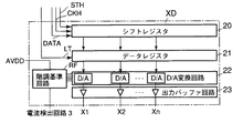
外部駆動回路PCBは、パーソナルコンピュータ等の信号源SGからデジタル形式で出力された映像データ信号DATAを受け取り、有機ELパネルPNLを駆動するために様々な制御信号を生成し、さらに映像データ信号DATAの並び替え等のデジタル処理を行うICチップからなるコントローラ部1、外部から供給される電源電圧を安定化して様々なレベルの内部電源電圧に変換するDC/DCコンバータ2を有する。コントローラ部1は様々な制御信号として例えば垂直走査制御信号CTYおよび水平走査制御信号CTXを発生する。ここで、垂直走査制御信号CTYは垂直スタート信号、垂直クロック信号を含む。水平走査制御信号CTXは水平スタート信号STH、水平クロック信号CKH、ラッチ信号LTを含む。垂直走査制御信号CTYはコントローラ部1から走査線駆動回路YDに供給され、水平走査制御信号CTXおよび映像データ信号DATAはコントローラ部1から信号線駆動回路XDに供給される。
【0014】
この外部駆動回路PCBはテープ・キャリア・パッケージ部TCPを介して有機ELパネルPNLに接続される。テープ・キャリア・パッケージ部TCPは各々フレキシブル配線基板上に駆動ICを実装した複数のテープ・キャリア・パッケージを並べたもので、n本の信号線X1,X2,X3,…Xnを映像信号に対応して駆動する信号線駆動回路XDおよび電源線VSSと電源線DVSSとの間に接続される電流検出回路3を含む。
【0015】
走査線駆動回路YDは垂直スタート信号を垂直クロック信号に同期してシフトすることによりm本の走査線Yを水平走査期間のうちの有効映像期間に順次選択するゲート駆動電圧(走査信号)を選択走査線Yに供給する。
【0016】
信号線駆動回路XDは、図2に示すように、水平スタート信号STHを水平クロック信号CKHに同期してシフトし、コントロール部1からの映像データ信号DATAを直並列変換するシフトレジスタ20、ラッチ信号LTの制御によりシフトレジスタ20から出力される映像データ信号DATAを順次取り込み保持し出力するデータレジスタ21、映像データ信号DATAをアナログ映像信号Vsigに変換するD/A変換回路22、このD/A変換回路22により参照される所定数の階調基準電圧VREF(V1〜Vk)を生成する階調基準回路RF、およびD/A変換回路22から得られるアナログ映像信号Vsigを電流増幅して信号線X1,X2,X3,…Xnに出力する出力バッファ回路23を含む。
【0017】
階調基準回路RFは図3に示すように電源線AVDDおよび電流検出回路3の出力端間に直列接続された抵抗R0〜Rkからなるラダー抵抗30を有し、ラダー抵抗30に印加される基準電源電圧を分圧して所定数の階調基準電圧VREF(V1〜Vk)を生成する。ここで、V1は最低階調の階調基準電圧であり、Vkは最高階調の階調基準電圧である。
【0018】
D/A変換回路22は各々データレジスタ21から供給される映像データ信号DATAに基づき所定数の階調基準電圧V1〜Vkのいずれかを選択し、さらにこれを抵抗分圧して対応するアナログ映像信号Vsigを出力する複数のD/A変換部(いわゆる抵抗DAC)で構成されている。出力バッファ回路23は各々対応D/A変換部からのアナログ映像信号Vsigを対応信号線Xに出力する複数のバッファアンプで構成される。
【0019】
各表示画素部PXは、DC/DCコンバータ2から電源線VDDおよびDVSS間に供給される画素駆動用電源電圧の下で動作する。走査線Yの走査信号が高レベルの期間、画素スイッチ11のNチャネル薄膜トランジスタがアクティブ状態であるため、信号線X上のアナログ映像信号Vsigが容量素子12の一端側電極に印加され、この容量素子12を充電する。尚、容量素子12の一端側電極に最終的にホールドされる電圧は、走査線Yの走査信号が低レベルとなった時に信号線Xに設定されているアナログ映像信号Vsigである。容量素子12の一端側電極はさらに電流駆動素子13のPチャネル薄膜トランジスタのゲートに接続され、他端側電極はこのPチャネル薄膜トランジスタのソースに接続されているため、容量素子12に充電された電圧は、Pチャネル型薄膜トランジスタのゲート−ソース間電圧Vgsとなる。Pチャネル型薄膜トランジスタのドレイン−ソース間電流Idsはゲート−ソース間Vgsによって増減する。この場合、電流Idsは有機EL素子10に流れる電流と同じであるため、アナログ映像信号Vsigによって有機EL素子10に流れる電流が変化し、この電流に対応する輝度で発光する。
【0020】
電流駆動素子13はPチャネル薄膜トランジスタであるため、図4に示すようにアナログ映像信号Vsigが小さいほど電源線VDDから各有機EL素子10を介して電源線VSSに流れる駆動電流DIDDは大きくなる。また、アナログ映像信号Vsigと映像データ信号の階調とは図5に示すようにアナログ映像信号Vsigが小さいほど階調値が大きくなる、つまり輝度を高めるような関係にある。
【0021】
上述の電流検出回路3は電源線VDDから複数の有機EL素子10を介して電源線VSSに流れる駆動電流DIDDの合計値Ielを検出するもので、抵抗ReおよびオペアンプAMPにより構成される。抵抗Reでの降下電圧Veはこの駆動電流DIDDの合計値Ielに依存して変化し、オペアンプAMPがこの降下電圧Veにほぼ等しいボルテージフォロワ電圧Ve’を出力端から出力する。
【0022】
この場合、階調基準回路RFのラダー抵抗30に印加される基準電源電圧は電流検出回路3から出力される電圧Ve’により補正される。具体的には、階調基準電圧Vkが電流検出回路3の出力電圧Ve’にほぼ等しく維持されるため、電圧Ve’が駆動電流DIDDの合計値Ielの増大に伴って増大すると、電圧Vkもこの増大分だけ図4に太い矢印で示すようにシフトする。このよう電圧Vkがシフトしても、電圧Vkと電圧V1との差はラダー抵抗30により等分されるため、映像信号Vsigと階調とは図5に示すものとほぼ同等の関係に維持される。
【0023】
上述した有機EL表示装置では、図6に示すように最高階調の基準階調電圧Vk(≒Ve’≒Ve)が従来のように一定でなく、この合計値Ielの増大に伴って上昇する。また、電圧Vkの上昇は、Pチャネル薄膜トランジスタである電流駆動素子13によって供給される駆動電流DIDDの合計値Ielを制限する結果となり、最終的には電圧Vkと駆動電流DIDDの合計値Ielとは電気的に平衡状態のところで保たれ、駆動電流DIDDの合計値Ielが定電流となる。
【0024】
図7に示すように、例えば従来では白表示部分の面積率が大きくなるにつれ、合計値Ielが大きくなるが、本発明は最高階調の階調基準電圧Vkが高くなるため合計値Ielの増加を抑えることができ、白表示部分の面積率が小さい時は高輝度で各有機EL素子10を発光させ、白表示部分の面積率が大きい時は低輝度で各有機EL素子10を発光させることにより全有機EL素子10で消費される駆動電流DIDDの合計値Ielに依存した電源回路の負担を軽減することが可能となる。
【0025】
尚、高階調大面積表示時、つまり白表示部分の面積率が大きいときは、輝度を下げても表示視認上目立たない。
【0026】
このように、駆動電流DIDDの総量に応じて輝度調整を行うことで、電力消費を抑制することが可能となる。
【0027】
また、駆動電流DIDDの総量の増大にともなうパネルの発熱を低減することができ、有機EL素子の劣化を抑制することができる。
【0028】
尚、本発明は上述の実施形態に限定されず、その要旨を逸脱しない範囲で様々に変形可能である。
【0029】
上述の実施形態では、映像信号の書き込みが電圧信号で行われる場合の表示画素について説明したが、これに限定されず、例えば図9に示すような電流信号で駆動されるものであってもよい。このような表示画素を有する表示装置に本発明を適用する場合の一例となる階調基準回路について説明する。つまり上述の実施形態では階調基準回路RFが所定数の階調基準電圧を発生するように構成されたが、D/A変換回路22が電流制御型である場合には、階調基準回路が図8に示すように基準電源電流に対して互いに異なる電流比に設定される所定数の階調基準電流IREF(I1からIk)をそれぞれ所定数の階調基準信号として出力するように接続した複数のカレントミラー能動素子からなるカレントミラー回路により構成される。具体的には、k+1個の薄膜トランジスタがカレントミラー能動素子として設けられる。第1の薄膜トランジスタのカレントパスは電源線AVDDおよび電流検出回路3の出力端間に接続され、ゲートは電源線AVDD側となる自身のドレインに接続される。残りk個の薄膜トランジスタのゲートは第1の薄膜トランジスタのゲートに共通に接続され、カレントパスは電源線AVDDおよびD/A変換回路22側に設けられたk個の階調基準電流入力端間にそれぞれ接続される。また、k個の薄膜トランジスタは第1の薄膜トランジスタのチャネル幅Wに対して、例えばチャネル幅W,2W,4W,8W,16W...2K−1Wを持つように設定される。これにより、第1の薄膜トランジスタに流れる電流を基準電源電流とし、これに対して互いに異なる電流比の階調基準電流I1からIkをD/A変換回路22に供給することになる。
【0030】
階調基準回路RFが上述のように構成される場合でも、階調基準電流I1からIkが電流検出回路3の出力電圧Ve’により一律にレベル補正する事ができるため、上述の実施形態と同様の効果を得ることができる。
【0031】
また、上述の実施形態では、単一の階調基準回路RFが全てのD/A変換回路22に対して共通に用いられたが、有機EL素子のような自己発光素子の発光特性は赤、緑、青のような発光色に対応して大きく異なる場合には、これら発光特性の種類に対応する複数の階調基準回路を設け、これら階調基準回路の各々について上述のような電流検出回路3を接続すればよい。
【0032】
【発明の効果】
以上のように本発明によれば、表示状態に違和感を与えることなく電源回路の負担を軽減できる表示装置を提供することができる。また、電力消費を抑制し、パネル発熱による素子劣化を抑制できる表示装置を提供することができる。
【図面の簡単な説明】
【図1】本発明の一実施形態に係る有機EL表示装置の回路構成を概略的に示す図である。
【図2】図1に示す信号線駆動回路の構成を示す図である。
【図3】図1に示す階調基準回路および電流検出回路の構成を示す図である。
【図4】図1に示す信号線に出力されるアナログ映像信号と有機EL素子に流れる駆動電流との関係を示すグラフである。
【図5】図1に示す信号線に出力されるアナログ映像信号と映像データ信号の階調との関係を示すグラフである。
【図6】図1に示す複数の有機EL素子に流れる駆動電流の合計値と最高階調の階調基準電圧出力との関係を示す図である。
【図7】図1に示す表示画面の白表示面積率と複数の有機EL素子に流れる駆動電流の合計値との関係を示すグラフである。
【図8】図3に示す階調基準回路を電流制御型のD/A変換回路に適用するための変形例の構成を示す図である。
【図9】表示画素の変形例を示す図である。
【符号の説明】
1…コントローラ部
2…DC/DCコンバータ
3…電流検出回路
10…有機EL素子
11…画素スイッチ
12…容量素子
13…電流駆動素子
Y…走査線
X…信号線
XD…信号線駆動回路
YD…走査線駆動回路
PX…表示画素部
PNL…有機ELパネル
PCB…外部回路基板
RF…階調基準回路
TCT…テープ・キャリア・パッケージ部
【発明の属する技術分野】
本発明は、複数の表示画素が例えば有機EL素子のような自己発光素子を用いて構成される表示装置に関する。
【0002】
【従来の技術】
近年では、有機EL表示装置のような平面表示装置が注目され、パーソナルコンピュータ、情報携帯端末等の表示装置として盛んに研究開発が行われている。この有機EL表示装置は、有機EL表示装置は薄型軽量化の妨げとなるバックライトを必要とせず、高速な応答性から動画再生に適し、さらに低温で輝度低下しないために寒冷地でも使用できるという特徴を有する。
【0003】
この有機EL表示装置は、一般に供給電流量に対応する輝度で発光する有機EL素子を用いた複数の表示画素のマトリクスアレイおよびこれら表示画素をそれぞれ駆動する駆動回路を備える。駆動回路は例えばデジタル映像信号をアナログ映像信号に変換するD/A変換回路およびこのD/A変換回路によって参照される複数の階調基準電圧または電流を発生する階調基準回路を含む。この階調基準回路が例えば基準電源電圧を分圧してこれら階調基準電圧を発生する場合、D/A変換回路はデジタル映像信号に基づいてこれら階調基準電圧のいずれかを選択しアナログ映像信号として出力する。各表示素子はこのアナログ映像信号に基づいて駆動される。
【0004】
上述の有機EL表示装置では、表示画面の明るさが複数の有機EL素子にそれぞれ流れる電流に依存する。複数の有機EL素子を最高輝度で発光させて表示画面全体を白表示とする場合には、大きな電力がこれら有機EL素子にそれぞれ流れる電流の和に対応して消費される結果となる。また、この電力消費はこれら有機EL素子に流れる電流に見合った電源回路の電流供給能力を要求することから、電源回路の製造コストおよび外形寸法の増大を招く。
【0005】
【発明が解決しようとする課題】
有機EL表示装置が組み込まれる機器に依存した例えば製造コスト、消費電力、容積等の制約により上述の問題を回避する必要がある場合、従来は白表示用の輝度を暗く設定してこれら有機EL素子に流れる電流を低下させるようにしている。しかしながら、白表示部分の面積が表示画面全体の面積に対して少ない場合の輝度も暗いという印象を与えてしまう。
【0006】
本発明の目的は高階調表示の場合での電力消費を低減可能な表示装置を提供することにある。また、本発明の別の目的は、電源回路の負担を軽減できる表示装置を提供することにある。
【0007】
【課題を解決するための手段】
本発明によれば、表示画面を構成する複数の自己発光素子と、映像信号に対応した駆動電流をこれら複数の自己発光素子にそれぞれ供給する駆動回路とを備え、この駆動回路はこれら複数の自己発光素子に流れる駆動電流の合計値の増大に伴って駆動電流を制限するように構成される表示装置が提供される。
【0008】
この表示装置では、駆動回路がこれら複数の自己発光素子に流れる駆動電流の合計値の増大に伴って駆動電流を制限する。駆動電流の合計値は白表示部分の面積割合が表示画面全体に対して多くなった場合に著しく増大するが、この場合に複数の自己発光素子の輝度が駆動電流の制限により一律に低下するため、電源回路の負担を軽減できる。従って、電源回路の製造コストおよび外形寸法の増大を回避することができる。他方、白表示部分の面積割合が表示画面全体に対して少ない場合には、自己発光素子にそれぞれ流れる電流が表示画面全体を白表示にするときのように制限されないため、白表示部分が著しく暗いという印象を与えることも回避できる。上述のような理由から、本表示装置は白表示部分の面積割合に依存した明るさについて違和感を与えることなく電源回路の負担を軽減するきとが可能となる。
【0009】
【発明の実施の形態】
以下、本発明の一実施形態に係る有機EL表示装置について図面を参照して説明する。
【0010】
図1は有機EL表示装置の回路構成を概略的に示し、図2は図1に示す信号線駆動回路の構成を示し、図3は図1に示す階調基準回路および電流検出回路の構成を示す。この有機EL表示装置は有機ELパネルPNLと、外部回路基板PCBと、有機ELパネルPNLおよび外部回路基板PCB間に接続されるテープキャリアパッケージTCPを備える。
【0011】
有機ELパネルPNLは、例えばガラス基板上にマトリクス状に配置され表示画面DSを構成する複数の表示画素部PX、これら表示画素部PXの行に沿って配置されるm本の走査線Y(Y1〜Ym)これら走査線Yに略直交する方向に配置されるn本の信号線X(X1〜Xn)、およびこれら走査線Y1〜Ymを駆動する走査線駆動回路YDを含む。行方向に隣接する3個の表示画素部PXは1個のカラー表示画素を構成し、それぞれ赤色(R)、緑色(G)、および青色(B)で発光する。各表示画素部PXはこれらRGBのうちの対応色で発光する自己発光素子となる有機EL素子10、対応走査線Yからの制御により対応信号線X上のアナログ映像信号Vsigを取り込む画素スイッチ11、この画素スイッチ11からの映像信号Vsigを保持する容量素子12、およびこの容量素子12に保持される映像信号Vsigの制御により有機EL素子10に駆動電流DIDDを流す電流駆動素子13を含む。画素スイッチ11は例えばNチャネルポリシリコン薄膜トランジスタからなり、電流駆動用素子13は例えばPチャネルポリシリコン薄膜トランジスタからなる。有機EL素子10は電源線VDD,VSS間で電流駆動素子13と直列に接続される。
【0012】
具体的には、有機EL素子10がカソードにおいて電源線VSSに接続され、アノードにおいて電流駆動素子13の薄膜トランジスタのドレインに接続される。この電流駆動素子13の薄膜トランジスタはゲートにおいて画素スイッチ11の薄膜トランジスタのドレインに接続され、ソース電極において電源線VDDに接続される。画素スイッチ11の薄膜トランジスタはソース電極において信号線Xに接続され、ゲート電極において走査線Yに接続される。容量素子12は電源線VDDと電流駆動素子13の薄膜トランジスタのゲートおよび画素スイッチ11の薄膜トランジスタのドレインを結ぶ配線により形成される。尚、上述の走査線駆動回路YDは表示画素部PXの薄膜トランジスタと同一プロセスで形成される複数のPおよびNチャネルポリシリコン薄膜トランジスタの組み合わせにより構成される。
【0013】
外部駆動回路PCBは、パーソナルコンピュータ等の信号源SGからデジタル形式で出力された映像データ信号DATAを受け取り、有機ELパネルPNLを駆動するために様々な制御信号を生成し、さらに映像データ信号DATAの並び替え等のデジタル処理を行うICチップからなるコントローラ部1、外部から供給される電源電圧を安定化して様々なレベルの内部電源電圧に変換するDC/DCコンバータ2を有する。コントローラ部1は様々な制御信号として例えば垂直走査制御信号CTYおよび水平走査制御信号CTXを発生する。ここで、垂直走査制御信号CTYは垂直スタート信号、垂直クロック信号を含む。水平走査制御信号CTXは水平スタート信号STH、水平クロック信号CKH、ラッチ信号LTを含む。垂直走査制御信号CTYはコントローラ部1から走査線駆動回路YDに供給され、水平走査制御信号CTXおよび映像データ信号DATAはコントローラ部1から信号線駆動回路XDに供給される。
【0014】
この外部駆動回路PCBはテープ・キャリア・パッケージ部TCPを介して有機ELパネルPNLに接続される。テープ・キャリア・パッケージ部TCPは各々フレキシブル配線基板上に駆動ICを実装した複数のテープ・キャリア・パッケージを並べたもので、n本の信号線X1,X2,X3,…Xnを映像信号に対応して駆動する信号線駆動回路XDおよび電源線VSSと電源線DVSSとの間に接続される電流検出回路3を含む。
【0015】
走査線駆動回路YDは垂直スタート信号を垂直クロック信号に同期してシフトすることによりm本の走査線Yを水平走査期間のうちの有効映像期間に順次選択するゲート駆動電圧(走査信号)を選択走査線Yに供給する。
【0016】
信号線駆動回路XDは、図2に示すように、水平スタート信号STHを水平クロック信号CKHに同期してシフトし、コントロール部1からの映像データ信号DATAを直並列変換するシフトレジスタ20、ラッチ信号LTの制御によりシフトレジスタ20から出力される映像データ信号DATAを順次取り込み保持し出力するデータレジスタ21、映像データ信号DATAをアナログ映像信号Vsigに変換するD/A変換回路22、このD/A変換回路22により参照される所定数の階調基準電圧VREF(V1〜Vk)を生成する階調基準回路RF、およびD/A変換回路22から得られるアナログ映像信号Vsigを電流増幅して信号線X1,X2,X3,…Xnに出力する出力バッファ回路23を含む。
【0017】
階調基準回路RFは図3に示すように電源線AVDDおよび電流検出回路3の出力端間に直列接続された抵抗R0〜Rkからなるラダー抵抗30を有し、ラダー抵抗30に印加される基準電源電圧を分圧して所定数の階調基準電圧VREF(V1〜Vk)を生成する。ここで、V1は最低階調の階調基準電圧であり、Vkは最高階調の階調基準電圧である。
【0018】
D/A変換回路22は各々データレジスタ21から供給される映像データ信号DATAに基づき所定数の階調基準電圧V1〜Vkのいずれかを選択し、さらにこれを抵抗分圧して対応するアナログ映像信号Vsigを出力する複数のD/A変換部(いわゆる抵抗DAC)で構成されている。出力バッファ回路23は各々対応D/A変換部からのアナログ映像信号Vsigを対応信号線Xに出力する複数のバッファアンプで構成される。
【0019】
各表示画素部PXは、DC/DCコンバータ2から電源線VDDおよびDVSS間に供給される画素駆動用電源電圧の下で動作する。走査線Yの走査信号が高レベルの期間、画素スイッチ11のNチャネル薄膜トランジスタがアクティブ状態であるため、信号線X上のアナログ映像信号Vsigが容量素子12の一端側電極に印加され、この容量素子12を充電する。尚、容量素子12の一端側電極に最終的にホールドされる電圧は、走査線Yの走査信号が低レベルとなった時に信号線Xに設定されているアナログ映像信号Vsigである。容量素子12の一端側電極はさらに電流駆動素子13のPチャネル薄膜トランジスタのゲートに接続され、他端側電極はこのPチャネル薄膜トランジスタのソースに接続されているため、容量素子12に充電された電圧は、Pチャネル型薄膜トランジスタのゲート−ソース間電圧Vgsとなる。Pチャネル型薄膜トランジスタのドレイン−ソース間電流Idsはゲート−ソース間Vgsによって増減する。この場合、電流Idsは有機EL素子10に流れる電流と同じであるため、アナログ映像信号Vsigによって有機EL素子10に流れる電流が変化し、この電流に対応する輝度で発光する。
【0020】
電流駆動素子13はPチャネル薄膜トランジスタであるため、図4に示すようにアナログ映像信号Vsigが小さいほど電源線VDDから各有機EL素子10を介して電源線VSSに流れる駆動電流DIDDは大きくなる。また、アナログ映像信号Vsigと映像データ信号の階調とは図5に示すようにアナログ映像信号Vsigが小さいほど階調値が大きくなる、つまり輝度を高めるような関係にある。
【0021】
上述の電流検出回路3は電源線VDDから複数の有機EL素子10を介して電源線VSSに流れる駆動電流DIDDの合計値Ielを検出するもので、抵抗ReおよびオペアンプAMPにより構成される。抵抗Reでの降下電圧Veはこの駆動電流DIDDの合計値Ielに依存して変化し、オペアンプAMPがこの降下電圧Veにほぼ等しいボルテージフォロワ電圧Ve’を出力端から出力する。
【0022】
この場合、階調基準回路RFのラダー抵抗30に印加される基準電源電圧は電流検出回路3から出力される電圧Ve’により補正される。具体的には、階調基準電圧Vkが電流検出回路3の出力電圧Ve’にほぼ等しく維持されるため、電圧Ve’が駆動電流DIDDの合計値Ielの増大に伴って増大すると、電圧Vkもこの増大分だけ図4に太い矢印で示すようにシフトする。このよう電圧Vkがシフトしても、電圧Vkと電圧V1との差はラダー抵抗30により等分されるため、映像信号Vsigと階調とは図5に示すものとほぼ同等の関係に維持される。
【0023】
上述した有機EL表示装置では、図6に示すように最高階調の基準階調電圧Vk(≒Ve’≒Ve)が従来のように一定でなく、この合計値Ielの増大に伴って上昇する。また、電圧Vkの上昇は、Pチャネル薄膜トランジスタである電流駆動素子13によって供給される駆動電流DIDDの合計値Ielを制限する結果となり、最終的には電圧Vkと駆動電流DIDDの合計値Ielとは電気的に平衡状態のところで保たれ、駆動電流DIDDの合計値Ielが定電流となる。
【0024】
図7に示すように、例えば従来では白表示部分の面積率が大きくなるにつれ、合計値Ielが大きくなるが、本発明は最高階調の階調基準電圧Vkが高くなるため合計値Ielの増加を抑えることができ、白表示部分の面積率が小さい時は高輝度で各有機EL素子10を発光させ、白表示部分の面積率が大きい時は低輝度で各有機EL素子10を発光させることにより全有機EL素子10で消費される駆動電流DIDDの合計値Ielに依存した電源回路の負担を軽減することが可能となる。
【0025】
尚、高階調大面積表示時、つまり白表示部分の面積率が大きいときは、輝度を下げても表示視認上目立たない。
【0026】
このように、駆動電流DIDDの総量に応じて輝度調整を行うことで、電力消費を抑制することが可能となる。
【0027】
また、駆動電流DIDDの総量の増大にともなうパネルの発熱を低減することができ、有機EL素子の劣化を抑制することができる。
【0028】
尚、本発明は上述の実施形態に限定されず、その要旨を逸脱しない範囲で様々に変形可能である。
【0029】
上述の実施形態では、映像信号の書き込みが電圧信号で行われる場合の表示画素について説明したが、これに限定されず、例えば図9に示すような電流信号で駆動されるものであってもよい。このような表示画素を有する表示装置に本発明を適用する場合の一例となる階調基準回路について説明する。つまり上述の実施形態では階調基準回路RFが所定数の階調基準電圧を発生するように構成されたが、D/A変換回路22が電流制御型である場合には、階調基準回路が図8に示すように基準電源電流に対して互いに異なる電流比に設定される所定数の階調基準電流IREF(I1からIk)をそれぞれ所定数の階調基準信号として出力するように接続した複数のカレントミラー能動素子からなるカレントミラー回路により構成される。具体的には、k+1個の薄膜トランジスタがカレントミラー能動素子として設けられる。第1の薄膜トランジスタのカレントパスは電源線AVDDおよび電流検出回路3の出力端間に接続され、ゲートは電源線AVDD側となる自身のドレインに接続される。残りk個の薄膜トランジスタのゲートは第1の薄膜トランジスタのゲートに共通に接続され、カレントパスは電源線AVDDおよびD/A変換回路22側に設けられたk個の階調基準電流入力端間にそれぞれ接続される。また、k個の薄膜トランジスタは第1の薄膜トランジスタのチャネル幅Wに対して、例えばチャネル幅W,2W,4W,8W,16W...2K−1Wを持つように設定される。これにより、第1の薄膜トランジスタに流れる電流を基準電源電流とし、これに対して互いに異なる電流比の階調基準電流I1からIkをD/A変換回路22に供給することになる。
【0030】
階調基準回路RFが上述のように構成される場合でも、階調基準電流I1からIkが電流検出回路3の出力電圧Ve’により一律にレベル補正する事ができるため、上述の実施形態と同様の効果を得ることができる。
【0031】
また、上述の実施形態では、単一の階調基準回路RFが全てのD/A変換回路22に対して共通に用いられたが、有機EL素子のような自己発光素子の発光特性は赤、緑、青のような発光色に対応して大きく異なる場合には、これら発光特性の種類に対応する複数の階調基準回路を設け、これら階調基準回路の各々について上述のような電流検出回路3を接続すればよい。
【0032】
【発明の効果】
以上のように本発明によれば、表示状態に違和感を与えることなく電源回路の負担を軽減できる表示装置を提供することができる。また、電力消費を抑制し、パネル発熱による素子劣化を抑制できる表示装置を提供することができる。
【図面の簡単な説明】
【図1】本発明の一実施形態に係る有機EL表示装置の回路構成を概略的に示す図である。
【図2】図1に示す信号線駆動回路の構成を示す図である。
【図3】図1に示す階調基準回路および電流検出回路の構成を示す図である。
【図4】図1に示す信号線に出力されるアナログ映像信号と有機EL素子に流れる駆動電流との関係を示すグラフである。
【図5】図1に示す信号線に出力されるアナログ映像信号と映像データ信号の階調との関係を示すグラフである。
【図6】図1に示す複数の有機EL素子に流れる駆動電流の合計値と最高階調の階調基準電圧出力との関係を示す図である。
【図7】図1に示す表示画面の白表示面積率と複数の有機EL素子に流れる駆動電流の合計値との関係を示すグラフである。
【図8】図3に示す階調基準回路を電流制御型のD/A変換回路に適用するための変形例の構成を示す図である。
【図9】表示画素の変形例を示す図である。
【符号の説明】
1…コントローラ部
2…DC/DCコンバータ
3…電流検出回路
10…有機EL素子
11…画素スイッチ
12…容量素子
13…電流駆動素子
Y…走査線
X…信号線
XD…信号線駆動回路
YD…走査線駆動回路
PX…表示画素部
PNL…有機ELパネル
PCB…外部回路基板
RF…階調基準回路
TCT…テープ・キャリア・パッケージ部
Claims (5)
- 表示画面を構成する複数の自己発光素子と、映像信号に対応した駆動電流を前記複数の自己発光素子にそれぞれ供給する駆動回路とを備え、前記駆動回路は前記複数の自己発光素子に流れる駆動電流の合計値の増大に伴って前記駆動電流を制限するように構成されることを特徴とする表示装置。
- 前記駆動回路は前記映像信号をデジタル形式からアナログ形式に変換するD/A変換回路と、前記D/A変換回路によって参照される所定数の階調基準信号を発生する階調基準回路と、前記複数の自己発光素子に流れる駆動電流の合計値を検出し、この合計値に対応して前記階調基準回路から発生される所定数の階調基準信号を一律にレベル補正する補正回路とを含むことを特徴とする請求項1に記載の表示装置。
- 前記階調基準回路は基準電源電圧に対して互いに異なる電圧比に設定される所定数の階調基準電圧をそれぞれ前記所定数の階調基準信号として出力するように接続した複数の抵抗素子からなる分圧回路を含むことを特徴とする請求項2に記載の表示装置。
- 前記階調基準回路は基準電源電流に対して互いに異なる電流比に設定される所定数の階調基準電流をそれぞれ前記所定数の階調基準信号として出力するように接続した複数のカレントミラー能動素子からなるカレントミラー回路を含むことを特徴とする請求項2に記載の表示装置。
- 前記自己発光素子は有機エレクトロルミネッセンス素子からなることを特徴とする請求項1に記載の表示装置。
Priority Applications (4)
| Application Number | Priority Date | Filing Date | Title |
|---|---|---|---|
| JP2002329712A JP2004163673A (ja) | 2002-11-13 | 2002-11-13 | 表示装置 |
| TW092131528A TWI244630B (en) | 2002-11-13 | 2003-11-11 | Display device |
| KR1020030079724A KR100610711B1 (ko) | 2002-11-13 | 2003-11-12 | 표시 장치 |
| US10/705,972 US7193592B2 (en) | 2002-11-13 | 2003-11-13 | Display device |
Applications Claiming Priority (1)
| Application Number | Priority Date | Filing Date | Title |
|---|---|---|---|
| JP2002329712A JP2004163673A (ja) | 2002-11-13 | 2002-11-13 | 表示装置 |
Publications (1)
| Publication Number | Publication Date |
|---|---|
| JP2004163673A true JP2004163673A (ja) | 2004-06-10 |
Family
ID=32290048
Family Applications (1)
| Application Number | Title | Priority Date | Filing Date |
|---|---|---|---|
| JP2002329712A Pending JP2004163673A (ja) | 2002-11-13 | 2002-11-13 | 表示装置 |
Country Status (4)
| Country | Link |
|---|---|
| US (1) | US7193592B2 (ja) |
| JP (1) | JP2004163673A (ja) |
| KR (1) | KR100610711B1 (ja) |
| TW (1) | TWI244630B (ja) |
Cited By (6)
| Publication number | Priority date | Publication date | Assignee | Title |
|---|---|---|---|---|
| JP2006119618A (ja) * | 2004-09-21 | 2006-05-11 | Casio Comput Co Ltd | ディスプレイパネル、その駆動方法及びその製造方法 |
| JP2006189806A (ja) * | 2004-12-06 | 2006-07-20 | Semiconductor Energy Lab Co Ltd | 表示装置及びその駆動方法 |
| JP2007121988A (ja) * | 2005-09-30 | 2007-05-17 | Seiko Epson Corp | 表示方法、表示装置及び電子機器 |
| JP2009205124A (ja) * | 2008-02-28 | 2009-09-10 | Samsung Mobile Display Co Ltd | 有機電界発光表示装置、および有機電界発光表示装置の駆動方法 |
| US7737923B2 (en) | 2005-09-16 | 2010-06-15 | Semiconductor Energy Laboratory Co., Ltd. | Display device and driving method of display device |
| US7911427B2 (en) | 2005-08-01 | 2011-03-22 | Samsung Mobile Display Co., Ltd. | Voltage based data driving circuit, light emitting display using the same, and method of driving the light emitting display |
Families Citing this family (17)
| Publication number | Priority date | Publication date | Assignee | Title |
|---|---|---|---|---|
| KR100589385B1 (ko) * | 2004-01-29 | 2006-06-14 | 삼성에스디아이 주식회사 | 발광 표시 장치 및 그 계조 전압 생성 방법 |
| KR100604058B1 (ko) * | 2004-09-24 | 2006-07-24 | 삼성에스디아이 주식회사 | 직류/직류 변환기와 이를 이용한 발광 표시장치 및 그의구동방법 |
| KR100658620B1 (ko) * | 2004-10-08 | 2006-12-15 | 삼성에스디아이 주식회사 | 전류 샘플/홀드 회로, 및 이를 이용한 표시 장치 및 그표시 패널과 구동 방법 |
| KR100590060B1 (ko) * | 2004-10-08 | 2006-06-14 | 삼성에스디아이 주식회사 | 계조 전류 생성 회로와 이를 이용한 표시 장치 및 그 표시패널과 구동 방법 |
| US8294648B2 (en) | 2004-10-08 | 2012-10-23 | Samsung Display Co., Ltd. | Gray-scale current generating circuit, display device using the same, and display panel and driving method thereof |
| KR100571647B1 (ko) * | 2005-03-31 | 2006-04-17 | 주식회사 하이닉스반도체 | 반도체 장치의 데이터 래치회로 |
| JP4379416B2 (ja) * | 2005-04-26 | 2009-12-09 | エプソンイメージングデバイス株式会社 | Led駆動回路、照明装置および電気光学装置 |
| KR100827642B1 (ko) * | 2006-04-25 | 2008-05-07 | 에스케이텔레시스 주식회사 | 방열구조를 가지는 이동통신 중계기 |
| KR100786509B1 (ko) * | 2006-06-08 | 2007-12-17 | 삼성에스디아이 주식회사 | 유기전계발광표시장치 및 그의 구동방법 |
| CN101681583B (zh) | 2007-05-16 | 2012-12-12 | 皇家飞利浦电子股份有限公司 | 用于显示器屏幕的动态功率控制 |
| TWI404011B (zh) * | 2009-03-18 | 2013-08-01 | Pervasive Display Co Ltd | 非揮發性顯示模組及非揮發性顯示裝置 |
| DE102009030176B4 (de) * | 2009-06-24 | 2014-02-06 | Init Innovative Informatikanwendungen In Transport-, Verkehrs- Und Leitsystemen Gmbh | Anordnung zur Ansteuerung von Licht emittierenden Dioden |
| DE102009030174B4 (de) * | 2009-06-24 | 2013-11-07 | Init Innovative Informatikanwendungen In Transport-, Verkehrs- Und Leitsystemen Gmbh | Schaltungsanordnung zur Ansteuerung von Licht emittierenden Dioden und Anzeigetafel |
| KR102115530B1 (ko) * | 2012-12-12 | 2020-05-27 | 삼성디스플레이 주식회사 | 표시 장치 및 그 구동 방법 |
| JP2014182345A (ja) * | 2013-03-21 | 2014-09-29 | Sony Corp | 階調電圧発生回路及び表示装置 |
| JP2014182346A (ja) | 2013-03-21 | 2014-09-29 | Sony Corp | 階調電圧発生回路及び表示装置 |
| CN110767170B (zh) * | 2019-11-05 | 2020-11-10 | 深圳市华星光电半导体显示技术有限公司 | 画面显示方法及画面显示装置 |
Family Cites Families (8)
| Publication number | Priority date | Publication date | Assignee | Title |
|---|---|---|---|---|
| US4812642A (en) * | 1986-04-24 | 1989-03-14 | Alps Electric Co., Ltd. | Optical coordinate system input device |
| KR100296872B1 (ko) | 1993-07-22 | 2001-10-24 | 김순택 | 전계방출표시소자로이루어지는디스플레이패널의자동휘도보정장치및그구동방법 |
| JPH08314414A (ja) * | 1995-05-12 | 1996-11-29 | Sony Corp | プラズマアドレス表示装置 |
| KR100569734B1 (ko) | 1997-12-31 | 2006-08-18 | 삼성전자주식회사 | 프로그램 가능한 감마 기준전압 발생회로 및 이를 이용한 액정표시 장치 |
| KR20010059960A (ko) | 1999-12-31 | 2001-07-06 | 김영남 | 전류미러를 이용한 전계방출표시기의 캐소드 구동회로 |
| US6628252B2 (en) * | 2000-05-12 | 2003-09-30 | Rohm Co., Ltd. | LED drive circuit |
| US6747623B2 (en) * | 2001-02-09 | 2004-06-08 | Semiconductor Energy Laboratory Co., Ltd. | Liquid crystal display device and method of driving the same |
| JP2003150115A (ja) * | 2001-08-29 | 2003-05-23 | Seiko Epson Corp | 電流生成回路、半導体集積回路、電気光学装置および電子機器 |
-
2002
- 2002-11-13 JP JP2002329712A patent/JP2004163673A/ja active Pending
-
2003
- 2003-11-11 TW TW092131528A patent/TWI244630B/zh not_active IP Right Cessation
- 2003-11-12 KR KR1020030079724A patent/KR100610711B1/ko active IP Right Grant
- 2003-11-13 US US10/705,972 patent/US7193592B2/en active Active
Cited By (8)
| Publication number | Priority date | Publication date | Assignee | Title |
|---|---|---|---|---|
| JP2006119618A (ja) * | 2004-09-21 | 2006-05-11 | Casio Comput Co Ltd | ディスプレイパネル、その駆動方法及びその製造方法 |
| JP2006189806A (ja) * | 2004-12-06 | 2006-07-20 | Semiconductor Energy Lab Co Ltd | 表示装置及びその駆動方法 |
| US7911427B2 (en) | 2005-08-01 | 2011-03-22 | Samsung Mobile Display Co., Ltd. | Voltage based data driving circuit, light emitting display using the same, and method of driving the light emitting display |
| US7737923B2 (en) | 2005-09-16 | 2010-06-15 | Semiconductor Energy Laboratory Co., Ltd. | Display device and driving method of display device |
| US8743030B2 (en) | 2005-09-16 | 2014-06-03 | Semiconductor Energy Laboratory Co., Ltd. | Display device and driving method of display device |
| JP2007121988A (ja) * | 2005-09-30 | 2007-05-17 | Seiko Epson Corp | 表示方法、表示装置及び電子機器 |
| JP2009205124A (ja) * | 2008-02-28 | 2009-09-10 | Samsung Mobile Display Co Ltd | 有機電界発光表示装置、および有機電界発光表示装置の駆動方法 |
| US8154196B2 (en) | 2008-02-28 | 2012-04-10 | Samsung Mobile Display Co., Ltd. | Organic light emitting display with improved power supply control and method of driving the same |
Also Published As
| Publication number | Publication date |
|---|---|
| KR20040042846A (ko) | 2004-05-20 |
| US20040095340A1 (en) | 2004-05-20 |
| TWI244630B (en) | 2005-12-01 |
| KR100610711B1 (ko) | 2006-08-09 |
| US7193592B2 (en) | 2007-03-20 |
| TW200425012A (en) | 2004-11-16 |
Similar Documents
| Publication | Publication Date | Title |
|---|---|---|
| KR100610711B1 (ko) | 표시 장치 | |
| KR100885966B1 (ko) | 유기 발광 표시 장치 및 그 구동 방법 | |
| US7375705B2 (en) | Reference voltage generation circuit, data driver, display device, and electronic instrument | |
| KR100842511B1 (ko) | 화상 표시 장치 | |
| KR101089050B1 (ko) | 반도체 장치 | |
| US7379044B2 (en) | Image display apparatus | |
| US7999768B2 (en) | Organic light emitting diode display and driving method thereof | |
| CN112349243B (zh) | 显示装置 | |
| KR100535286B1 (ko) | 표시 장치 및 그 구동 방법 | |
| US20050110720A1 (en) | Image display device | |
| KR100565390B1 (ko) | 표시 장치 | |
| US20050007392A1 (en) | Electro-optical device, method of driving electro-optical device, and electronic apparatus | |
| JP2006106696A (ja) | デジタル/アナログコンバータとこれを利用した表示装置,およびその表示パネルと駆動方法 | |
| JP2005134435A (ja) | 画像表示装置 | |
| US10546530B2 (en) | Pixel driving circuit and display device thereof | |
| JP5780650B2 (ja) | レベルシフタ回路、走査回路、表示装置、及び、電子機器 | |
| WO2004100119A1 (ja) | 電流出力型半導体回路、表示駆動用ソースドライバ、表示装置、電流出力方法 | |
| US8094097B2 (en) | Data line driving circuit, electro-optical device, data line driving method, and electronic apparatus | |
| JP4216558B2 (ja) | 表示装置およびその駆動方法 | |
| US7800562B2 (en) | Display device | |
| JP2012098334A (ja) | 発光素子表示装置 | |
| JP4752177B2 (ja) | 表示装置の駆動回路、表示装置の駆動方法、電気光学装置及び電子機器 | |
| KR20070101545A (ko) | 표시 장치 | |
| JP2006337992A (ja) | 表示装置の駆動方法 | |
| JP2004138946A (ja) | アクティブマトリクス型表示装置 |
Legal Events
| Date | Code | Title | Description |
|---|---|---|---|
| A621 | Written request for application examination |
Free format text: JAPANESE INTERMEDIATE CODE: A621 Effective date: 20051107 |
|
| A711 | Notification of change in applicant |
Free format text: JAPANESE INTERMEDIATE CODE: A711 Effective date: 20070514 |
|
| A131 | Notification of reasons for refusal |
Free format text: JAPANESE INTERMEDIATE CODE: A131 Effective date: 20090210 |
|
| A02 | Decision of refusal |
Free format text: JAPANESE INTERMEDIATE CODE: A02 Effective date: 20090609 |