JP2004111912A - ポリシリコンの平坦化方法およびその方法から得られるポリシリコンからなる薄膜トランジスタ - Google Patents
ポリシリコンの平坦化方法およびその方法から得られるポリシリコンからなる薄膜トランジスタ Download PDFInfo
- Publication number
- JP2004111912A JP2004111912A JP2003181382A JP2003181382A JP2004111912A JP 2004111912 A JP2004111912 A JP 2004111912A JP 2003181382 A JP2003181382 A JP 2003181382A JP 2003181382 A JP2003181382 A JP 2003181382A JP 2004111912 A JP2004111912 A JP 2004111912A
- Authority
- JP
- Japan
- Prior art keywords
- polysilicon
- etching
- laser annealing
- laser
- substrate
- Prior art date
- Legal status (The legal status is an assumption and is not a legal conclusion. Google has not performed a legal analysis and makes no representation as to the accuracy of the status listed.)
- Pending
Links
- 229910021420 polycrystalline silicon Inorganic materials 0.000 title claims abstract description 86
- 229920005591 polysilicon Polymers 0.000 title claims abstract description 83
- 238000000034 method Methods 0.000 title claims abstract description 57
- 239000010409 thin film Substances 0.000 title claims abstract description 11
- 238000005224 laser annealing Methods 0.000 claims abstract description 23
- 238000005530 etching Methods 0.000 claims abstract description 21
- 239000000758 substrate Substances 0.000 claims abstract description 15
- 230000003746 surface roughness Effects 0.000 claims description 26
- KRHYYFGTRYWZRS-UHFFFAOYSA-N Fluorane Chemical compound F KRHYYFGTRYWZRS-UHFFFAOYSA-N 0.000 claims description 13
- 238000001039 wet etching Methods 0.000 claims description 11
- XLYOFNOQVPJJNP-UHFFFAOYSA-N water Substances O XLYOFNOQVPJJNP-UHFFFAOYSA-N 0.000 claims description 7
- 238000001312 dry etching Methods 0.000 claims description 6
- 239000002904 solvent Substances 0.000 claims description 6
- XUIMIQQOPSSXEZ-UHFFFAOYSA-N Silicon Chemical compound [Si] XUIMIQQOPSSXEZ-UHFFFAOYSA-N 0.000 claims description 5
- 229910052710 silicon Inorganic materials 0.000 claims description 5
- 239000010703 silicon Substances 0.000 claims description 5
- 239000011521 glass Substances 0.000 claims description 4
- 230000001590 oxidative effect Effects 0.000 claims description 4
- 239000007789 gas Substances 0.000 claims description 3
- 229910000040 hydrogen fluoride Inorganic materials 0.000 claims description 3
- 238000002156 mixing Methods 0.000 claims description 3
- 239000000203 mixture Substances 0.000 claims description 3
- 238000001020 plasma etching Methods 0.000 claims description 3
- 239000010453 quartz Substances 0.000 claims description 3
- VYPSYNLAJGMNEJ-UHFFFAOYSA-N silicon dioxide Inorganic materials O=[Si]=O VYPSYNLAJGMNEJ-UHFFFAOYSA-N 0.000 claims description 3
- 239000000243 solution Substances 0.000 description 8
- 230000015572 biosynthetic process Effects 0.000 description 4
- 239000010408 film Substances 0.000 description 4
- 238000004519 manufacturing process Methods 0.000 description 4
- 238000010586 diagram Methods 0.000 description 3
- 230000000694 effects Effects 0.000 description 3
- 230000005684 electric field Effects 0.000 description 3
- 239000012535 impurity Substances 0.000 description 3
- 239000000126 substance Substances 0.000 description 3
- 229910017855 NH 4 F Inorganic materials 0.000 description 2
- 230000015556 catabolic process Effects 0.000 description 2
- 239000011159 matrix material Substances 0.000 description 2
- 238000011160 research Methods 0.000 description 2
- 230000002411 adverse Effects 0.000 description 1
- 238000000149 argon plasma sintering Methods 0.000 description 1
- 238000005229 chemical vapour deposition Methods 0.000 description 1
- 238000011161 development Methods 0.000 description 1
- 238000007429 general method Methods 0.000 description 1
- 239000012212 insulator Substances 0.000 description 1
- 238000005499 laser crystallization Methods 0.000 description 1
- 239000004973 liquid crystal related substance Substances 0.000 description 1
- 239000011259 mixed solution Substances 0.000 description 1
- 239000012299 nitrogen atmosphere Substances 0.000 description 1
- 239000002245 particle Substances 0.000 description 1
- 238000000206 photolithography Methods 0.000 description 1
- 238000005498 polishing Methods 0.000 description 1
- 238000011946 reduction process Methods 0.000 description 1
- 239000004065 semiconductor Substances 0.000 description 1
- 238000012546 transfer Methods 0.000 description 1
Images


Classifications
-
- H—ELECTRICITY
- H01—ELECTRIC ELEMENTS
- H01L—SEMICONDUCTOR DEVICES NOT COVERED BY CLASS H10
- H01L29/00—Semiconductor devices specially adapted for rectifying, amplifying, oscillating or switching and having potential barriers; Capacitors or resistors having potential barriers, e.g. a PN-junction depletion layer or carrier concentration layer; Details of semiconductor bodies or of electrodes thereof ; Multistep manufacturing processes therefor
- H01L29/66—Types of semiconductor device ; Multistep manufacturing processes therefor
- H01L29/66007—Multistep manufacturing processes
- H01L29/66075—Multistep manufacturing processes of devices having semiconductor bodies comprising group 14 or group 13/15 materials
- H01L29/66227—Multistep manufacturing processes of devices having semiconductor bodies comprising group 14 or group 13/15 materials the devices being controllable only by the electric current supplied or the electric potential applied, to an electrode which does not carry the current to be rectified, amplified or switched, e.g. three-terminal devices
- H01L29/66409—Unipolar field-effect transistors
- H01L29/66477—Unipolar field-effect transistors with an insulated gate, i.e. MISFET
- H01L29/66742—Thin film unipolar transistors
- H01L29/6675—Amorphous silicon or polysilicon transistors
-
- H—ELECTRICITY
- H01—ELECTRIC ELEMENTS
- H01L—SEMICONDUCTOR DEVICES NOT COVERED BY CLASS H10
- H01L29/00—Semiconductor devices specially adapted for rectifying, amplifying, oscillating or switching and having potential barriers; Capacitors or resistors having potential barriers, e.g. a PN-junction depletion layer or carrier concentration layer; Details of semiconductor bodies or of electrodes thereof ; Multistep manufacturing processes therefor
- H01L29/66—Types of semiconductor device ; Multistep manufacturing processes therefor
- H01L29/68—Types of semiconductor device ; Multistep manufacturing processes therefor controllable by only the electric current supplied, or only the electric potential applied, to an electrode which does not carry the current to be rectified, amplified or switched
- H01L29/76—Unipolar devices, e.g. field effect transistors
- H01L29/772—Field effect transistors
- H01L29/78—Field effect transistors with field effect produced by an insulated gate
- H01L29/786—Thin film transistors, i.e. transistors with a channel being at least partly a thin film
- H01L29/78603—Thin film transistors, i.e. transistors with a channel being at least partly a thin film characterised by the insulating substrate or support
-
- H—ELECTRICITY
- H01—ELECTRIC ELEMENTS
- H01L—SEMICONDUCTOR DEVICES NOT COVERED BY CLASS H10
- H01L29/00—Semiconductor devices specially adapted for rectifying, amplifying, oscillating or switching and having potential barriers; Capacitors or resistors having potential barriers, e.g. a PN-junction depletion layer or carrier concentration layer; Details of semiconductor bodies or of electrodes thereof ; Multistep manufacturing processes therefor
- H01L29/66—Types of semiconductor device ; Multistep manufacturing processes therefor
- H01L29/68—Types of semiconductor device ; Multistep manufacturing processes therefor controllable by only the electric current supplied, or only the electric potential applied, to an electrode which does not carry the current to be rectified, amplified or switched
- H01L29/76—Unipolar devices, e.g. field effect transistors
- H01L29/772—Field effect transistors
- H01L29/78—Field effect transistors with field effect produced by an insulated gate
- H01L29/786—Thin film transistors, i.e. transistors with a channel being at least partly a thin film
- H01L29/78651—Silicon transistors
- H01L29/7866—Non-monocrystalline silicon transistors
- H01L29/78672—Polycrystalline or microcrystalline silicon transistor
- H01L29/78675—Polycrystalline or microcrystalline silicon transistor with normal-type structure, e.g. with top gate
Landscapes
- Engineering & Computer Science (AREA)
- Microelectronics & Electronic Packaging (AREA)
- Power Engineering (AREA)
- Ceramic Engineering (AREA)
- Condensed Matter Physics & Semiconductors (AREA)
- General Physics & Mathematics (AREA)
- Physics & Mathematics (AREA)
- Computer Hardware Design (AREA)
- Manufacturing & Machinery (AREA)
- Chemical & Material Sciences (AREA)
- Crystallography & Structural Chemistry (AREA)
- Recrystallisation Techniques (AREA)
- Weting (AREA)
- Thin Film Transistor (AREA)
Abstract
【課題】本発明は、大面積のポリシリコン表面に応用出来る、ポリシリコンの平坦化方法および該方法により得られたポリシリコンからなる薄膜トランジスタを提供する。
【解決手段】基板の表面にポリシリコンを形成する工程、エッチングにより表面粗さを減少させる工程、および該ポリシリコン表面をレーザーアニールにより平坦化する工程からなるポリシリコンの平坦化方法である。
【選択図】 図2
【解決手段】基板の表面にポリシリコンを形成する工程、エッチングにより表面粗さを減少させる工程、および該ポリシリコン表面をレーザーアニールにより平坦化する工程からなるポリシリコンの平坦化方法である。
【選択図】 図2
Description
【0001】
【発明の属する技術分野】
本発明は、エッチングとレーザーアニールにより、表面粗さを減少させるポリシリコンの平坦化方法および該方法により得られたポリシリコンからなる薄膜トランジスタに関する。
【0002】
【従来の技術】
ポリシリコン薄膜トランジスタ(thin film transistor、TFT)は、アクティブマトリクス液晶ディスプレイ、アクティブマトリクス有機発光ディスプレイ(Active matrix organic light emitting display)、エスラムSRAM、プロジェクタ、およびコンパクトイメージセンサなど、様々な領域において、幅広く採用されている。
【0003】
現在のポリシリコンTFTは、表面構造が粗いため、素子の電気的特性(ブレークダウン電界、漏電、閾値下の振れ、臨界電圧、および電子/ホールの移動率等)に悪影響を及ぼす。また、ポリシリコンの粒子が大きくなるほど、表面が粗くなるため、状況はさらに悪化する。
【0004】
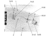
ポリシリコンの表面粗さは、製品の品質に直接影響を及ぼす。例えば、半導体製造工程において、ゲート酸化層をポリシリコン上に形成する場合、図1で示されるように、ポリシリコン層2の厚さが不均衡なため、その上部に形成されたゲート酸化層1の厚さも不均一になり、ポリシリコン層2中の隆起により、局部で大きい電界を形成し、ゲート酸化層1がブレークダウンし易くなり、漏電を増加させ、素子の信頼度に影響を与える。特に、薄いゲート酸化層を形成する場合では、さらに深刻な問題となる。
【0005】
さらに、フォトグラフィ工程において、ポリシリコンの表面の凹凸により、光散乱が生じ、尺寸定義を誤らせるため、工程中のパターン定義を困難にする。
【0006】
ポリシリコンの表面粗さに関して、化学機械研磨(chemical mechanical polishing、CMP)が提案されている(例えば、非特許文献1参照)。これによると、CMPにより、ポリシリコンの表面粗さは90Åから37Åに減少し、電子/ホール移動度、臨界電圧、閾値下の振れを改善することができる。
【0007】
また、CMPにより改善されたポリシリコン表面粗さが、TFT素子性能の効果を向上させることが開示されている(例えば、非特許文献2参照)。
【0008】
しかし、これらの方法では、大面積のポリシリコンの量産には適しておらず、ポリシリコンTFTの発展に伴い、大面積の基板(1m×1m、あるいは、それ以上)を用いて、大量に、尺寸の素子(例えば、低温ポリシリコンLTPS TFTなどの小さい素子)を製造する方法としては適さない。また、CMP後の表面粗さは、30〜40Åもあり、尺寸が極小化する趨勢下で、ポリシリコンの表面をさらに滑らかにする必要がある。
【0009】
したがって、未だ、大面積のポリシリコンの平坦化工程に適応できる方法であって、表面粗さを減少できる方法はない。
【0010】
【非特許文献1】
C.Y.Changら、米国電気電子技術者協会IEEE(international electrical and electronic engineering)の電子装置レター(electron device letter)1996年3月、VOL.17、No3、“Fabrication of thin film transistor by chemical mechanical polished polycrystalline silicon film”研究報告
【非特許文献2】
Alain C.K.Chanら、IEEE電子装置会議1999議事録、“Improve Thin−Film Transistor(TFT) Characteristics on chemical−mechanically polished polycrystalline silicon film”研究報告
【0011】
【発明が解決しようとする課題】
本発明は、大面積のポリシリコン表面に応用出来る、ポリシリコンの平坦化方法および該方法により得られたポリシリコンからなる薄膜トランジスタを提供する。
【0012】
【課題を解決するための手段】
すなわち、本発明は、基板の表面にポリシリコンを形成する工程、エッチングにより表面粗さを減少させる工程、および該ポリシリコン表面をレーザーアニールにより平坦化する工程からなるポリシリコンの平坦化方法に関する。
【0013】
エッチングが、ドライエッチングであることが好ましい。
【0014】
エッチングが、湿式エッチングであることが好ましい。
【0015】
湿式エッチングの溶剤が、緩衝酸化エッチング溶液または希フッ化水素酸であることが好ましい。
【0016】
湿式エッチング溶剤が、緩衝酸化エッチング溶液と水からなり、その混合比率が、1:300〜1:0であることが好ましい。
【0017】
希フッ化水素酸が、フッ化水素と水を1:600〜1:1で混合したものであることが好ましい。
【0018】
湿式エッチングの時間が、600秒以下であることが好ましい。
【0019】
ドライエッチングが、CF4ガスを用いたプラズマエッチングであることが好ましい。
【0020】
レーザーアニールのレーザーパルスの波長が、157〜351nmであることが好ましい。
【0021】
レーザーアニールのレーザーパルスの時間が、10ns〜1msであることが好ましい。
【0022】
レーザーアニールの基板の温度が、室温〜600℃であることが好ましい。
【0023】
レーザーアニールのレーザーパルスの周波数が、1Hz〜400Hzであることが好ましい。
【0024】
レーザーアニールのエネルギー密度が、ポリシリコンを完全に溶解する限界エネルギー密度より低いことが好ましい。
【0025】
レーザーアニールのエネルギー密度が、250〜350mJ/cm2であることが好ましい。
【0026】
基板が、ガラス、石英、シリコンウエハ、プラスチック、SOIであることが好ましい。
【0027】
本発明は、前記方法により製造されたポリシリコンからなる薄膜トランジスタに関する。
【0028】
【発明の実施の形態】
本発明のポリシリコン平坦化方法は、図2のフローチャートに示すように、4ポリシリコンの形成工程、5エッチングによる表面粗さ減少工程、および6ポリシリコン表面のレーザーアニールによる平坦化工程からなるポリシリコンの平坦化方法に関する。
【0029】
本発明に使用される基板は、ガラス、石英、シリコンウェハ、プラスチック、SOI(silicon on insulator)があげられるが、これらに限定されるものではなく、本発明の方法は、表面にポリシリコンを形成できる基板であればどのようなものでも使用することができる。
【0030】
ポリシリコンの形成工程により、表面にポリシリコンを形成した基板が提供される。ポリシリコンの形成方法は、レーザー結晶法あるいは、化学気相蒸着法などの方法があげられるが、これらに限定されるものではなく、一般的な形成方法であればいずれの方法も採用できる。また、ポリシリコンの形成工程により得られたポリシリコンの表面粗さは、約100Å以下である。
【0031】
つぎに、エッチングによる表面粗さ減少工程では、エッチングによりポリシリコンの表面を変化させ、自然酸化層、弱いボンディング部分、ポリシリコンの不純物などの不要物が除去され、表面粗さを初期的に減少することができる。エッチング方法としては、ドライエッチング、湿式エッチングがあげられる。
【0032】
ドライエッチングの方法は、一般的な方法であれば特に限定されないが、中でもCF4ガスによるプラズマエッチングが好ましい。
【0033】
湿式エッチングにおいて使用される溶剤は、緩衝酸化エッチング(buffered oxide etchant、BOE)溶液または希フッ化水素酸(diluted hydrofluoric acid、DHF)からなる溶剤が、ポリシリコン表面の自然酸化膜、表面の不純物、およびポリシリコンの結合が比較的弱い部分をエッチングすることができる点で好ましい。
【0034】
BOE溶液の組成は、NH4F(40%):HF(49%)が1:1〜200:1の混合溶液であることが好ましい。
【0035】
BOE溶液は、水で希釈することが好ましく、その混合比率は、BOE溶液:水が、1:300〜1:0が好ましい。
【0036】
DHFは、フッ化水素と水を1:600〜1:1で混合することが好ましい。
【0037】
湿式エッチングの時間は、600秒以下であることが好ましい。
【0038】
ポリシリコン表面のレーザーアニールによる平坦化工程は、レーザーアニールによりポリシリコン表面を部分的に溶解して、格子構造が再構成され、表面が平坦化され、表面粗さを減少することができる。
【0039】
使用するレーザーとしては、特に限定されるものではないが、エキシマレーザー(excimer laser)などがあげられる。
【0040】
また、温度、圧力、レーザーエネルギー密度などのパラメータは、用いられる機器の型により異なるため、適宜調整することが好ましい。
【0041】
例えば、複パルス位相は、98%であることが好ましく、周囲の環境は、1atmの窒素雰囲気下であることが好ましい。
【0042】
周波数は、1〜400Hzであることが好ましく、200Hzであることがより好ましい。
【0043】
波長は、157〜351nmが好ましく、308nmであることがより好ましい。
【0044】
エネルギー密度は、ポリシリコンが完全に溶解する限界エネルギー密度より低いことが好ましく、250〜350mJ/cm2であることがより好ましい。
【0045】
レーザーパルスの時間は、10ns〜1msであることが好ましく、55nsであることがより好ましい。
【0046】
基板の温度は、室温〜600℃であることが好ましい。
【0047】
本発明の方法によると、エッチングによりその表面構造を変化させ、自然酸化物、弱いボンディング部分、およびポリシリコンの不純物を除去して、表面粗さを初期的に減少させた後、レーザーアニール工程を施し、ポリシリコンを部分的に溶解させ、ポリシリコンの表面が再構築され、平坦化した表面を形成することができ、さらに、大面積のポリシリコン表面に適用することが出来るという長所がある。また、本発明の方法により得られたポリシリコンからなる薄膜トランジスタは、表面が平坦化されたポリシリコンを用いるため、素子の電気的特性(ブレークダウン電界、漏電、閾値下の振れ、臨界電圧、および電子/ホールの移動率等)に優れる。
【0048】
【実施例】
以下、実施をあげて本発明をさらに詳しく説明するが、本発明はかかる実施例のみに限定されるものではない。
【0049】
実施例1
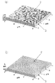
ポリシリコンを形成したガラス基板を、BOE溶液(BOE溶液:NH4F(40%):HF(49%)=20:1)に300秒間浸漬し、エッチングを行った。その後、エキシマレーザー(レーザーパルスの波長308nm、時間55ns、周波数200Hz、エネルギー密度350mJ/cm2、基板の温度25℃)により表面平坦化を行った。図3(a)は、平坦化される前のポリシリコンのTEM観察図(×100000倍)であり、図3(b)は、表面粗さが減少したポリシリコンのTEM観察図である。これより、未処理のポリシリコン(a)の隆起は、(b)の平坦な状態になり、ポリシリコンとゲート酸化層間の隆起がなく、滑らかなポリシリコン表面が得られることが分かる。また、図4(a)は、平坦化される前のポリシリコンのAFMの立体図(表面粗さは、約120Å)であり、図4(b)は、表面粗さが減少したポリシリコンのAFMの立体図(表面粗さは、約18Å)である。これより、ポリシリコンの表面粗さは、120Åから18Åに減少し、未処理の状態のわずか15%まで減少することがわかる。
【0050】
また、図5にレーザーパルスのエネルギー密度を変化させた結果を示す。未処理のポリシリコン(丸印)は、エッチング(三角印)およびレーザーアニール(四角印)工程後、ポリシリコン表面粗さが、未処理状態と比較して、30〜95%減少し、20Å以下まで減少する。CMPを用いる公知の方法(表面粗さ減少率50%)と比較して、本発明において提供される方法は、ポリシリコンを平坦化するとき、優れた効果を提供する。
【0051】
【発明の効果】
本発明の平坦化方法は、大面積のポリシリコン表面に応用出来、平坦化されたポリシリコンおよび該方法により得られたポリシリコンからなる薄膜トランジスタを提供することができる。
【図面の簡単な説明】
【図1】ポリシリコンとゲート酸化層のTEM観察画像である。
【図2】本発明の方法のフローチャートである。
【図3】(a)平坦化される前のポリシリコンのTEM観察像である。(b)表面粗さが減少したポリシリコンのTEM観察像である。
【図4】(a)平坦化される前のポリシリコンのAFM観察像である。(b)表面粗さが減少したポリシリコンのAFM観察像である。
【図5】未処理、エッチング後、レーザーアニール後のポリシリコン膜の表面粗さを示す図である。
【符号の説明】
1 ゲート酸化層
2 ポリシリコン層
3 基板
4 ポリシリコンの形成工程
5 エッチングによる表面粗さ減少工程
6 ポリシリコン表面のレーザーアニールによる平坦化工程
【発明の属する技術分野】
本発明は、エッチングとレーザーアニールにより、表面粗さを減少させるポリシリコンの平坦化方法および該方法により得られたポリシリコンからなる薄膜トランジスタに関する。
【0002】
【従来の技術】
ポリシリコン薄膜トランジスタ(thin film transistor、TFT)は、アクティブマトリクス液晶ディスプレイ、アクティブマトリクス有機発光ディスプレイ(Active matrix organic light emitting display)、エスラムSRAM、プロジェクタ、およびコンパクトイメージセンサなど、様々な領域において、幅広く採用されている。
【0003】
現在のポリシリコンTFTは、表面構造が粗いため、素子の電気的特性(ブレークダウン電界、漏電、閾値下の振れ、臨界電圧、および電子/ホールの移動率等)に悪影響を及ぼす。また、ポリシリコンの粒子が大きくなるほど、表面が粗くなるため、状況はさらに悪化する。
【0004】
ポリシリコンの表面粗さは、製品の品質に直接影響を及ぼす。例えば、半導体製造工程において、ゲート酸化層をポリシリコン上に形成する場合、図1で示されるように、ポリシリコン層2の厚さが不均衡なため、その上部に形成されたゲート酸化層1の厚さも不均一になり、ポリシリコン層2中の隆起により、局部で大きい電界を形成し、ゲート酸化層1がブレークダウンし易くなり、漏電を増加させ、素子の信頼度に影響を与える。特に、薄いゲート酸化層を形成する場合では、さらに深刻な問題となる。
【0005】
さらに、フォトグラフィ工程において、ポリシリコンの表面の凹凸により、光散乱が生じ、尺寸定義を誤らせるため、工程中のパターン定義を困難にする。
【0006】
ポリシリコンの表面粗さに関して、化学機械研磨(chemical mechanical polishing、CMP)が提案されている(例えば、非特許文献1参照)。これによると、CMPにより、ポリシリコンの表面粗さは90Åから37Åに減少し、電子/ホール移動度、臨界電圧、閾値下の振れを改善することができる。
【0007】
また、CMPにより改善されたポリシリコン表面粗さが、TFT素子性能の効果を向上させることが開示されている(例えば、非特許文献2参照)。
【0008】
しかし、これらの方法では、大面積のポリシリコンの量産には適しておらず、ポリシリコンTFTの発展に伴い、大面積の基板(1m×1m、あるいは、それ以上)を用いて、大量に、尺寸の素子(例えば、低温ポリシリコンLTPS TFTなどの小さい素子)を製造する方法としては適さない。また、CMP後の表面粗さは、30〜40Åもあり、尺寸が極小化する趨勢下で、ポリシリコンの表面をさらに滑らかにする必要がある。
【0009】
したがって、未だ、大面積のポリシリコンの平坦化工程に適応できる方法であって、表面粗さを減少できる方法はない。
【0010】
【非特許文献1】
C.Y.Changら、米国電気電子技術者協会IEEE(international electrical and electronic engineering)の電子装置レター(electron device letter)1996年3月、VOL.17、No3、“Fabrication of thin film transistor by chemical mechanical polished polycrystalline silicon film”研究報告
【非特許文献2】
Alain C.K.Chanら、IEEE電子装置会議1999議事録、“Improve Thin−Film Transistor(TFT) Characteristics on chemical−mechanically polished polycrystalline silicon film”研究報告
【0011】
【発明が解決しようとする課題】
本発明は、大面積のポリシリコン表面に応用出来る、ポリシリコンの平坦化方法および該方法により得られたポリシリコンからなる薄膜トランジスタを提供する。
【0012】
【課題を解決するための手段】
すなわち、本発明は、基板の表面にポリシリコンを形成する工程、エッチングにより表面粗さを減少させる工程、および該ポリシリコン表面をレーザーアニールにより平坦化する工程からなるポリシリコンの平坦化方法に関する。
【0013】
エッチングが、ドライエッチングであることが好ましい。
【0014】
エッチングが、湿式エッチングであることが好ましい。
【0015】
湿式エッチングの溶剤が、緩衝酸化エッチング溶液または希フッ化水素酸であることが好ましい。
【0016】
湿式エッチング溶剤が、緩衝酸化エッチング溶液と水からなり、その混合比率が、1:300〜1:0であることが好ましい。
【0017】
希フッ化水素酸が、フッ化水素と水を1:600〜1:1で混合したものであることが好ましい。
【0018】
湿式エッチングの時間が、600秒以下であることが好ましい。
【0019】
ドライエッチングが、CF4ガスを用いたプラズマエッチングであることが好ましい。
【0020】
レーザーアニールのレーザーパルスの波長が、157〜351nmであることが好ましい。
【0021】
レーザーアニールのレーザーパルスの時間が、10ns〜1msであることが好ましい。
【0022】
レーザーアニールの基板の温度が、室温〜600℃であることが好ましい。
【0023】
レーザーアニールのレーザーパルスの周波数が、1Hz〜400Hzであることが好ましい。
【0024】
レーザーアニールのエネルギー密度が、ポリシリコンを完全に溶解する限界エネルギー密度より低いことが好ましい。
【0025】
レーザーアニールのエネルギー密度が、250〜350mJ/cm2であることが好ましい。
【0026】
基板が、ガラス、石英、シリコンウエハ、プラスチック、SOIであることが好ましい。
【0027】
本発明は、前記方法により製造されたポリシリコンからなる薄膜トランジスタに関する。
【0028】
【発明の実施の形態】
本発明のポリシリコン平坦化方法は、図2のフローチャートに示すように、4ポリシリコンの形成工程、5エッチングによる表面粗さ減少工程、および6ポリシリコン表面のレーザーアニールによる平坦化工程からなるポリシリコンの平坦化方法に関する。
【0029】
本発明に使用される基板は、ガラス、石英、シリコンウェハ、プラスチック、SOI(silicon on insulator)があげられるが、これらに限定されるものではなく、本発明の方法は、表面にポリシリコンを形成できる基板であればどのようなものでも使用することができる。
【0030】
ポリシリコンの形成工程により、表面にポリシリコンを形成した基板が提供される。ポリシリコンの形成方法は、レーザー結晶法あるいは、化学気相蒸着法などの方法があげられるが、これらに限定されるものではなく、一般的な形成方法であればいずれの方法も採用できる。また、ポリシリコンの形成工程により得られたポリシリコンの表面粗さは、約100Å以下である。
【0031】
つぎに、エッチングによる表面粗さ減少工程では、エッチングによりポリシリコンの表面を変化させ、自然酸化層、弱いボンディング部分、ポリシリコンの不純物などの不要物が除去され、表面粗さを初期的に減少することができる。エッチング方法としては、ドライエッチング、湿式エッチングがあげられる。
【0032】
ドライエッチングの方法は、一般的な方法であれば特に限定されないが、中でもCF4ガスによるプラズマエッチングが好ましい。
【0033】
湿式エッチングにおいて使用される溶剤は、緩衝酸化エッチング(buffered oxide etchant、BOE)溶液または希フッ化水素酸(diluted hydrofluoric acid、DHF)からなる溶剤が、ポリシリコン表面の自然酸化膜、表面の不純物、およびポリシリコンの結合が比較的弱い部分をエッチングすることができる点で好ましい。
【0034】
BOE溶液の組成は、NH4F(40%):HF(49%)が1:1〜200:1の混合溶液であることが好ましい。
【0035】
BOE溶液は、水で希釈することが好ましく、その混合比率は、BOE溶液:水が、1:300〜1:0が好ましい。
【0036】
DHFは、フッ化水素と水を1:600〜1:1で混合することが好ましい。
【0037】
湿式エッチングの時間は、600秒以下であることが好ましい。
【0038】
ポリシリコン表面のレーザーアニールによる平坦化工程は、レーザーアニールによりポリシリコン表面を部分的に溶解して、格子構造が再構成され、表面が平坦化され、表面粗さを減少することができる。
【0039】
使用するレーザーとしては、特に限定されるものではないが、エキシマレーザー(excimer laser)などがあげられる。
【0040】
また、温度、圧力、レーザーエネルギー密度などのパラメータは、用いられる機器の型により異なるため、適宜調整することが好ましい。
【0041】
例えば、複パルス位相は、98%であることが好ましく、周囲の環境は、1atmの窒素雰囲気下であることが好ましい。
【0042】
周波数は、1〜400Hzであることが好ましく、200Hzであることがより好ましい。
【0043】
波長は、157〜351nmが好ましく、308nmであることがより好ましい。
【0044】
エネルギー密度は、ポリシリコンが完全に溶解する限界エネルギー密度より低いことが好ましく、250〜350mJ/cm2であることがより好ましい。
【0045】
レーザーパルスの時間は、10ns〜1msであることが好ましく、55nsであることがより好ましい。
【0046】
基板の温度は、室温〜600℃であることが好ましい。
【0047】
本発明の方法によると、エッチングによりその表面構造を変化させ、自然酸化物、弱いボンディング部分、およびポリシリコンの不純物を除去して、表面粗さを初期的に減少させた後、レーザーアニール工程を施し、ポリシリコンを部分的に溶解させ、ポリシリコンの表面が再構築され、平坦化した表面を形成することができ、さらに、大面積のポリシリコン表面に適用することが出来るという長所がある。また、本発明の方法により得られたポリシリコンからなる薄膜トランジスタは、表面が平坦化されたポリシリコンを用いるため、素子の電気的特性(ブレークダウン電界、漏電、閾値下の振れ、臨界電圧、および電子/ホールの移動率等)に優れる。
【0048】
【実施例】
以下、実施をあげて本発明をさらに詳しく説明するが、本発明はかかる実施例のみに限定されるものではない。
【0049】
実施例1
ポリシリコンを形成したガラス基板を、BOE溶液(BOE溶液:NH4F(40%):HF(49%)=20:1)に300秒間浸漬し、エッチングを行った。その後、エキシマレーザー(レーザーパルスの波長308nm、時間55ns、周波数200Hz、エネルギー密度350mJ/cm2、基板の温度25℃)により表面平坦化を行った。図3(a)は、平坦化される前のポリシリコンのTEM観察図(×100000倍)であり、図3(b)は、表面粗さが減少したポリシリコンのTEM観察図である。これより、未処理のポリシリコン(a)の隆起は、(b)の平坦な状態になり、ポリシリコンとゲート酸化層間の隆起がなく、滑らかなポリシリコン表面が得られることが分かる。また、図4(a)は、平坦化される前のポリシリコンのAFMの立体図(表面粗さは、約120Å)であり、図4(b)は、表面粗さが減少したポリシリコンのAFMの立体図(表面粗さは、約18Å)である。これより、ポリシリコンの表面粗さは、120Åから18Åに減少し、未処理の状態のわずか15%まで減少することがわかる。
【0050】
また、図5にレーザーパルスのエネルギー密度を変化させた結果を示す。未処理のポリシリコン(丸印)は、エッチング(三角印)およびレーザーアニール(四角印)工程後、ポリシリコン表面粗さが、未処理状態と比較して、30〜95%減少し、20Å以下まで減少する。CMPを用いる公知の方法(表面粗さ減少率50%)と比較して、本発明において提供される方法は、ポリシリコンを平坦化するとき、優れた効果を提供する。
【0051】
【発明の効果】
本発明の平坦化方法は、大面積のポリシリコン表面に応用出来、平坦化されたポリシリコンおよび該方法により得られたポリシリコンからなる薄膜トランジスタを提供することができる。
【図面の簡単な説明】
【図1】ポリシリコンとゲート酸化層のTEM観察画像である。
【図2】本発明の方法のフローチャートである。
【図3】(a)平坦化される前のポリシリコンのTEM観察像である。(b)表面粗さが減少したポリシリコンのTEM観察像である。
【図4】(a)平坦化される前のポリシリコンのAFM観察像である。(b)表面粗さが減少したポリシリコンのAFM観察像である。
【図5】未処理、エッチング後、レーザーアニール後のポリシリコン膜の表面粗さを示す図である。
【符号の説明】
1 ゲート酸化層
2 ポリシリコン層
3 基板
4 ポリシリコンの形成工程
5 エッチングによる表面粗さ減少工程
6 ポリシリコン表面のレーザーアニールによる平坦化工程
Claims (16)
- 基板の表面にポリシリコンを形成する工程、エッチングにより表面粗さを減少させる工程、および該ポリシリコン表面をレーザーアニールにより平坦化する工程からなるポリシリコンの平坦化方法。
- エッチングが、ドライエッチングである請求項1記載のポリシリコンの平坦化方法。
- エッチングが、湿式エッチングである請求項1記載のポリシリコンの平坦化方法。
- 湿式エッチングの溶剤が、緩衝酸化エッチング溶液または希フッ化水素酸である請求項3記載のポリシリコンの平坦化方法。
- 湿式エッチング溶剤が、緩衝酸化エッチング溶液と水からなり、その混合比率が、1:300〜1:0である請求項3記載のポリシリコンの平坦化方法。
- 希フッ化水素酸が、フッ化水素と水を1:600〜1:1で混合したものである請求項4記載のポリシリコンの平坦化方法。
- 湿式エッチングの時間が、600秒以下である請求項3、4、5または6記載のポリシリコンの平坦化方法。
- ドライエッチングが、CF4ガスを用いたプラズマエッチングである請求項2記載のポリシリコンの平坦化方法。
- レーザーアニールのレーザーパルスの波長が、157〜351nmである請求項1、2または3記載のポリシリコンの平坦化方法。
- レーザーアニールのレーザーパルスの時間が、10ns〜1msである請求項1、2または3記載のポリシリコンの平坦化方法。
- レーザーアニールの基板の温度が、室温〜600℃である請求項1、2または3記載のポリシリコンの平坦化方法。
- レーザーアニールのレーザーパルスの周波数が、1Hz〜400Hzである請求項1、2または3記載のポリシリコンの平坦化方法。
- レーザーアニールのエネルギー密度が、ポリシリコンを完全に溶解する限界エネルギー密度より低いエネルギー密度である請求項1、2または3記載のポリシリコンの平坦化方法。
- レーザーアニールのエネルギー密度が、250〜350mJ/cm2である請求項1、2または3記載のポリシリコンの平坦化方法。
- 基板が、ガラス、石英、シリコンウエハ、プラスチック、SOIである請求項1、2または3記載のポリシリコンの平坦化方法。
- 請求項1、2または3記載の方法により得られたポリシリコンからなる薄膜トランジスタ。
Applications Claiming Priority (1)
| Application Number | Priority Date | Filing Date | Title |
|---|---|---|---|
| TW091121425A TWI301641B (ja) | 2002-09-19 | 2002-09-19 |
Publications (1)
| Publication Number | Publication Date |
|---|---|
| JP2004111912A true JP2004111912A (ja) | 2004-04-08 |
Family
ID=31989760
Family Applications (1)
| Application Number | Title | Priority Date | Filing Date |
|---|---|---|---|
| JP2003181382A Pending JP2004111912A (ja) | 2002-09-19 | 2003-06-25 | ポリシリコンの平坦化方法およびその方法から得られるポリシリコンからなる薄膜トランジスタ |
Country Status (3)
| Country | Link |
|---|---|
| US (1) | US20040055999A1 (ja) |
| JP (1) | JP2004111912A (ja) |
| TW (1) | TWI301641B (ja) |
Cited By (1)
| Publication number | Priority date | Publication date | Assignee | Title |
|---|---|---|---|---|
| JP2007210191A (ja) * | 2006-02-09 | 2007-08-23 | Toppan Printing Co Ltd | モールドの欠陥修正方法及びモールド |
Families Citing this family (13)
| Publication number | Priority date | Publication date | Assignee | Title |
|---|---|---|---|---|
| TWI290768B (en) * | 2003-06-05 | 2007-12-01 | Au Optronics Corp | Method for manufacturing polysilicon film |
| TWI306667B (en) * | 2004-09-07 | 2009-02-21 | Ind Tech Res Inst | Method of fabricating planarized poly-silicon thin film transistors |
| CN100382255C (zh) * | 2004-09-24 | 2008-04-16 | 财团法人工业技术研究院 | 平坦多晶硅薄膜晶体管的制作方法 |
| SG121918A1 (en) * | 2004-10-27 | 2006-05-26 | Sony Corp | A method and system of treating a surface of a fabricated microcomponent |
| US7579654B2 (en) * | 2006-05-31 | 2009-08-25 | Corning Incorporated | Semiconductor on insulator structure made using radiation annealing |
| TWI325613B (en) * | 2006-07-20 | 2010-06-01 | Ind Tech Res Inst | Memory cell and fabricating method thereof |
| JP2009094488A (ja) * | 2007-09-21 | 2009-04-30 | Semiconductor Energy Lab Co Ltd | 半導体膜付き基板の作製方法 |
| JP5250228B2 (ja) * | 2007-09-21 | 2013-07-31 | 株式会社半導体エネルギー研究所 | 半導体装置の作製方法 |
| JP5452900B2 (ja) * | 2007-09-21 | 2014-03-26 | 株式会社半導体エネルギー研究所 | 半導体膜付き基板の作製方法 |
| JP5490393B2 (ja) * | 2007-10-10 | 2014-05-14 | 株式会社半導体エネルギー研究所 | 半導体基板の製造方法 |
| US8377804B2 (en) * | 2008-10-02 | 2013-02-19 | Semiconductor Energy Laboratory Co., Ltd. | Manufacturing method of semiconductor substrate and semiconductor device |
| US9455350B2 (en) | 2014-03-25 | 2016-09-27 | National Applied Research Laboratories | Transistor device structure that includes polycrystalline semiconductor thin film that has large grain size |
| CN105513959A (zh) | 2016-01-04 | 2016-04-20 | 京东方科技集团股份有限公司 | 一种多晶硅薄膜的处理方法和薄膜晶体管的制作方法 |
Family Cites Families (4)
| Publication number | Priority date | Publication date | Assignee | Title |
|---|---|---|---|---|
| US5202278A (en) * | 1991-09-10 | 1993-04-13 | Micron Technology, Inc. | Method of forming a capacitor in semiconductor wafer processing |
| US6393042B1 (en) * | 1999-03-08 | 2002-05-21 | Semiconductor Energy Laboratory Co., Ltd. | Beam homogenizer and laser irradiation apparatus |
| JP4101409B2 (ja) * | 1999-08-19 | 2008-06-18 | シャープ株式会社 | 半導体装置の製造方法 |
| JP2002043274A (ja) * | 2000-07-25 | 2002-02-08 | Kanto Chem Co Inc | ポリシリコン膜の表面処理剤及びそれを用いたポリシリコン膜の表面処理方法 |
-
2002
- 2002-09-19 TW TW091121425A patent/TWI301641B/zh not_active IP Right Cessation
-
2003
- 2003-02-05 US US10/358,184 patent/US20040055999A1/en not_active Abandoned
- 2003-06-25 JP JP2003181382A patent/JP2004111912A/ja active Pending
Cited By (1)
| Publication number | Priority date | Publication date | Assignee | Title |
|---|---|---|---|---|
| JP2007210191A (ja) * | 2006-02-09 | 2007-08-23 | Toppan Printing Co Ltd | モールドの欠陥修正方法及びモールド |
Also Published As
| Publication number | Publication date |
|---|---|
| TWI301641B (ja) | 2008-10-01 |
| US20040055999A1 (en) | 2004-03-25 |
Similar Documents
| Publication | Publication Date | Title |
|---|---|---|
| JP2004111912A (ja) | ポリシリコンの平坦化方法およびその方法から得られるポリシリコンからなる薄膜トランジスタ | |
| JP5038326B2 (ja) | 半導体素子の製造方法 | |
| KR20080101653A (ko) | 반도체 기판 및 반도체 장치 및 그 제조 방법 | |
| US20060043072A1 (en) | Method for planarizing polysilicon | |
| JP2000012864A (ja) | 半導体装置の作製方法 | |
| TW200937508A (en) | Substrate provided with semiconductor films and manufacturing method thereof | |
| JP4162211B2 (ja) | シリコンウエハの洗浄方法および洗浄されたシリコンウエハ | |
| US6228728B1 (en) | Method of fabricating semiconductor device | |
| US20060145158A1 (en) | Poly-crystalline silicon thin film transistor | |
| CN106328694B (zh) | 半导体结构的形成方法 | |
| US20060051905A1 (en) | Method of fabricating planarized poly-silicon thin film transistors | |
| JP2011135054A (ja) | Soi基板の作製方法およびsoi基板 | |
| WO2017136984A1 (zh) | N型薄膜晶体管的制作方法 | |
| JP2007158371A (ja) | 半導体装置の作製方法 | |
| JP4286692B2 (ja) | ポリシリコン結晶化の制御方法 | |
| US20100173472A1 (en) | Method for manufacturing soi substrate and method for manufacturing semiconductor device | |
| KR20060120765A (ko) | 반도체 장치의 제조 방법 | |
| US6482682B2 (en) | Manufacturing method for improving reliability of polysilicon thin film transistors | |
| JP2004056099A (ja) | 窒化珪素膜、並びに半導体装置及びその作製方法 | |
| US8815657B2 (en) | Method of manufacturing semiconductor device | |
| JP4282391B2 (ja) | 半導体装置の製造方法 | |
| CN104851802B (zh) | 一种半导体器件及其制作方法 | |
| JP3203652B2 (ja) | 半導体薄膜の製造方法 | |
| JP3302228B2 (ja) | Soi基板の作製方法 | |
| US10886121B2 (en) | Methods of reducing silicon consumption, methods of forming a semiconductor structure, and methods of forming isolation structures |