JP2001077517A5 - - Google Patents
Download PDFInfo
- Publication number
- JP2001077517A5 JP2001077517A5 JP1999247503A JP24750399A JP2001077517A5 JP 2001077517 A5 JP2001077517 A5 JP 2001077517A5 JP 1999247503 A JP1999247503 A JP 1999247503A JP 24750399 A JP24750399 A JP 24750399A JP 2001077517 A5 JP2001077517 A5 JP 2001077517A5
- Authority
- JP
- Japan
- Prior art keywords
- electrode pad
- bump
- protective film
- substrate
- electronic component
- Prior art date
- Legal status (The legal status is an assumption and is not a legal conclusion. Google has not performed a legal analysis and makes no representation as to the accuracy of the status listed.)
- Granted
Links
- 239000000758 substrate Substances 0.000 description 68
- 230000001681 protective effect Effects 0.000 description 67
- ATJFFYVFTNAWJD-UHFFFAOYSA-N Tin Chemical compound [Sn] ATJFFYVFTNAWJD-UHFFFAOYSA-N 0.000 description 31
- BQCADISMDOOEFD-UHFFFAOYSA-N Silver Chemical compound [Ag] BQCADISMDOOEFD-UHFFFAOYSA-N 0.000 description 25
- 229910052709 silver Inorganic materials 0.000 description 25
- 239000004332 silver Substances 0.000 description 25
- 229910045601 alloy Inorganic materials 0.000 description 16
- 239000000956 alloy Substances 0.000 description 16
- 239000000463 material Substances 0.000 description 16
- 238000004519 manufacturing process Methods 0.000 description 11
- BASFCYQUMIYNBI-UHFFFAOYSA-N platinum Chemical compound [Pt] BASFCYQUMIYNBI-UHFFFAOYSA-N 0.000 description 10
- 229910000679 solder Inorganic materials 0.000 description 10
- 230000000694 effects Effects 0.000 description 8
- 238000000034 method Methods 0.000 description 8
- 229910052697 platinum Inorganic materials 0.000 description 5
- 230000003746 surface roughness Effects 0.000 description 4
- PNEYBMLMFCGWSK-UHFFFAOYSA-N aluminium oxide Inorganic materials [O-2].[O-2].[O-2].[Al+3].[Al+3] PNEYBMLMFCGWSK-UHFFFAOYSA-N 0.000 description 3
- 238000009792 diffusion process Methods 0.000 description 3
- 239000011521 glass Substances 0.000 description 3
- 238000002844 melting Methods 0.000 description 3
- 230000008018 melting Effects 0.000 description 3
- 238000007650 screen-printing Methods 0.000 description 3
- KDLHZDBZIXYQEI-UHFFFAOYSA-N Palladium Chemical compound [Pd] KDLHZDBZIXYQEI-UHFFFAOYSA-N 0.000 description 2
- 238000007796 conventional method Methods 0.000 description 2
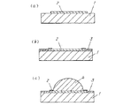
- 238000010586 diagram Methods 0.000 description 2
- 239000007772 electrode material Substances 0.000 description 2
- 239000000203 mixture Substances 0.000 description 2
- 238000005728 strengthening Methods 0.000 description 2
- 239000000126 substance Substances 0.000 description 2
- 229910001316 Ag alloy Inorganic materials 0.000 description 1
- QCEUXSAXTBNJGO-UHFFFAOYSA-N [Ag].[Sn] Chemical compound [Ag].[Sn] QCEUXSAXTBNJGO-UHFFFAOYSA-N 0.000 description 1
- 230000015572 biosynthetic process Effects 0.000 description 1
- 239000004020 conductor Substances 0.000 description 1
- 239000006071 cream Substances 0.000 description 1
- 235000012489 doughnuts Nutrition 0.000 description 1
- 238000005516 engineering process Methods 0.000 description 1
- 239000003822 epoxy resin Substances 0.000 description 1
- 238000010304 firing Methods 0.000 description 1
- -1 for example Chemical compound 0.000 description 1
- 239000007769 metal material Substances 0.000 description 1
- 229910052763 palladium Inorganic materials 0.000 description 1
- 229920000647 polyepoxide Polymers 0.000 description 1
- 238000007639 printing Methods 0.000 description 1
- 238000005096 rolling process Methods 0.000 description 1
- 230000001988 toxicity Effects 0.000 description 1
- 231100000419 toxicity Toxicity 0.000 description 1
Images


Priority Applications (1)
| Application Number | Priority Date | Filing Date | Title |
|---|---|---|---|
| JP24750399A JP4366777B2 (ja) | 1999-09-01 | 1999-09-01 | 電子部品 |
Applications Claiming Priority (1)
| Application Number | Priority Date | Filing Date | Title |
|---|---|---|---|
| JP24750399A JP4366777B2 (ja) | 1999-09-01 | 1999-09-01 | 電子部品 |
Publications (3)
| Publication Number | Publication Date |
|---|---|
| JP2001077517A JP2001077517A (ja) | 2001-03-23 |
| JP2001077517A5 true JP2001077517A5 (https=) | 2006-10-05 |
| JP4366777B2 JP4366777B2 (ja) | 2009-11-18 |
Family
ID=17164452
Family Applications (1)
| Application Number | Title | Priority Date | Filing Date |
|---|---|---|---|
| JP24750399A Expired - Fee Related JP4366777B2 (ja) | 1999-09-01 | 1999-09-01 | 電子部品 |
Country Status (1)
| Country | Link |
|---|---|
| JP (1) | JP4366777B2 (https=) |
Families Citing this family (2)
| Publication number | Priority date | Publication date | Assignee | Title |
|---|---|---|---|---|
| JP5043563B2 (ja) * | 2007-08-29 | 2012-10-10 | 新光電気工業株式会社 | 配線基板及びその製造方法 |
| JP7064325B2 (ja) * | 2017-12-18 | 2022-05-10 | スタンレー電気株式会社 | 半導体発光装置、および、それを用いた半導体発光装置の製造方法 |
-
1999
- 1999-09-01 JP JP24750399A patent/JP4366777B2/ja not_active Expired - Fee Related
Similar Documents
| Publication | Publication Date | Title |
|---|---|---|
| KR100846270B1 (ko) | 반도체장치 및 그 제조방법 | |
| JPH08162357A (ja) | セラミック電子部品 | |
| JPH0774450A (ja) | 電子回路装置 | |
| EP0766310A3 (en) | Solder bump structure | |
| US4268585A (en) | Soldering to a gold member | |
| JPS63107087A (ja) | 混成集積回路基板 | |
| EP0198354B1 (en) | Method for brazing interconnect pins to metallic pads | |
| KR100367314B1 (ko) | 반도체 장치 및 그의 제조방법 | |
| EP0945880A2 (en) | Surface-mount coil | |
| JP3356649B2 (ja) | 半導体装置及びその製造方法 | |
| JP3929675B2 (ja) | 圧電振動子 | |
| JPH04151843A (ja) | Icチップのボンディング方法 | |
| JP2012129318A (ja) | 半導体装置および半導体装置の製造方法 | |
| JP4011214B2 (ja) | 半導体装置及び半田による接合方法 | |
| EP1313143A2 (en) | Perimeter anchored thick film pad | |
| JP2001060760A (ja) | 回路電極およびその形成方法 | |
| JP2001077517A5 (https=) | ||
| JP4366777B2 (ja) | 電子部品 | |
| US6686665B1 (en) | Solder pad structure for low temperature co-fired ceramic package and method for making the same | |
| JPS59188147A (ja) | 半導体装置およびその製造方法 | |
| JP2803664B2 (ja) | 基板接続構造 | |
| JP2000138250A (ja) | 半導体装置およびその製造方法 | |
| JPH0982759A (ja) | 突起電極を有する基板の接続方法 | |
| JP3219022B2 (ja) | 電子部品搭載用セラミックス多層配線基板の電極構造 | |
| US4851301A (en) | Solder bonding with improved peel strength |