EP4565032A2 - Feldeffekttransistor mit ringverteilten feldeffekttransistorzellen - Google Patents
Feldeffekttransistor mit ringverteilten feldeffekttransistorzellen Download PDFInfo
- Publication number
- EP4565032A2 EP4565032A2 EP25162449.0A EP25162449A EP4565032A2 EP 4565032 A2 EP4565032 A2 EP 4565032A2 EP 25162449 A EP25162449 A EP 25162449A EP 4565032 A2 EP4565032 A2 EP 4565032A2
- Authority
- EP
- European Patent Office
- Prior art keywords
- fet
- gate
- disposed
- substrate
- drain
- Prior art date
- Legal status (The legal status is an assumption and is not a legal conclusion. Google has not performed a legal analysis and makes no representation as to the accuracy of the status listed.)
- Pending
Links
Images





Classifications
-
- H—ELECTRICITY
- H10—SEMICONDUCTOR DEVICES; ELECTRIC SOLID-STATE DEVICES NOT OTHERWISE PROVIDED FOR
- H10D—INORGANIC ELECTRIC SEMICONDUCTOR DEVICES
- H10D84/00—Integrated devices formed in or on semiconductor substrates that comprise only semiconducting layers, e.g. on Si wafers or on GaAs-on-Si wafers
- H10D84/80—Integrated devices formed in or on semiconductor substrates that comprise only semiconducting layers, e.g. on Si wafers or on GaAs-on-Si wafers characterised by the integration of at least one component covered by groups H10D12/00 or H10D30/00, e.g. integration of IGFETs
- H10D84/82—Integrated devices formed in or on semiconductor substrates that comprise only semiconducting layers, e.g. on Si wafers or on GaAs-on-Si wafers characterised by the integration of at least one component covered by groups H10D12/00 or H10D30/00, e.g. integration of IGFETs of only field-effect components
- H10D84/83—Integrated devices formed in or on semiconductor substrates that comprise only semiconducting layers, e.g. on Si wafers or on GaAs-on-Si wafers characterised by the integration of at least one component covered by groups H10D12/00 or H10D30/00, e.g. integration of IGFETs of only field-effect components of only insulated-gate FETs [IGFET]
-
- H—ELECTRICITY
- H10—SEMICONDUCTOR DEVICES; ELECTRIC SOLID-STATE DEVICES NOT OTHERWISE PROVIDED FOR
- H10D—INORGANIC ELECTRIC SEMICONDUCTOR DEVICES
- H10D30/00—Field-effect transistors [FET]
- H10D30/80—FETs having rectifying junction gate electrodes
- H10D30/87—FETs having Schottky gate electrodes, e.g. metal-semiconductor FETs [MESFET]
-
- H—ELECTRICITY
- H10—SEMICONDUCTOR DEVICES; ELECTRIC SOLID-STATE DEVICES NOT OTHERWISE PROVIDED FOR
- H10D—INORGANIC ELECTRIC SEMICONDUCTOR DEVICES
- H10D62/00—Semiconductor bodies, or regions thereof, of devices having potential barriers
- H10D62/10—Shapes, relative sizes or dispositions of the regions of the semiconductor bodies; Shapes of the semiconductor bodies
- H10D62/124—Shapes, relative sizes or dispositions of the regions of semiconductor bodies or of junctions between the regions
- H10D62/126—Top-view geometrical layouts of the regions or the junctions
- H10D62/127—Top-view geometrical layouts of the regions or the junctions of cellular field-effect devices, e.g. multicellular DMOS transistors or IGBTs
-
- H—ELECTRICITY
- H10—SEMICONDUCTOR DEVICES; ELECTRIC SOLID-STATE DEVICES NOT OTHERWISE PROVIDED FOR
- H10D—INORGANIC ELECTRIC SEMICONDUCTOR DEVICES
- H10D64/00—Electrodes of devices having potential barriers
- H10D64/20—Electrodes characterised by their shapes, relative sizes or dispositions
- H10D64/23—Electrodes carrying the current to be rectified, amplified, oscillated or switched, e.g. sources, drains, anodes or cathodes
- H10D64/251—Source or drain electrodes for field-effect devices
- H10D64/257—Source or drain electrodes for field-effect devices for lateral devices wherein the source or drain electrodes are characterised by top-view geometrical layouts, e.g. interdigitated, semi-circular, annular or L-shaped electrodes
-
- H—ELECTRICITY
- H10—SEMICONDUCTOR DEVICES; ELECTRIC SOLID-STATE DEVICES NOT OTHERWISE PROVIDED FOR
- H10D—INORGANIC ELECTRIC SEMICONDUCTOR DEVICES
- H10D64/00—Electrodes of devices having potential barriers
- H10D64/20—Electrodes characterised by their shapes, relative sizes or dispositions
- H10D64/27—Electrodes not carrying the current to be rectified, amplified, oscillated or switched, e.g. gates
- H10D64/311—Gate electrodes for field-effect devices
- H10D64/411—Gate electrodes for field-effect devices for FETs
-
- H—ELECTRICITY
- H10—SEMICONDUCTOR DEVICES; ELECTRIC SOLID-STATE DEVICES NOT OTHERWISE PROVIDED FOR
- H10D—INORGANIC ELECTRIC SEMICONDUCTOR DEVICES
- H10D64/00—Electrodes of devices having potential barriers
- H10D64/20—Electrodes characterised by their shapes, relative sizes or dispositions
- H10D64/27—Electrodes not carrying the current to be rectified, amplified, oscillated or switched, e.g. gates
- H10D64/311—Gate electrodes for field-effect devices
- H10D64/411—Gate electrodes for field-effect devices for FETs
- H10D64/511—Gate electrodes for field-effect devices for FETs for IGFETs
- H10D64/517—Gate electrodes for field-effect devices for FETs for IGFETs characterised by the conducting layers
- H10D64/519—Gate electrodes for field-effect devices for FETs for IGFETs characterised by the conducting layers characterised by their top-view geometrical layouts
-
- H—ELECTRICITY
- H10—SEMICONDUCTOR DEVICES; ELECTRIC SOLID-STATE DEVICES NOT OTHERWISE PROVIDED FOR
- H10W—GENERIC PACKAGES, INTERCONNECTIONS, CONNECTORS OR OTHER CONSTRUCTIONAL DETAILS OF DEVICES COVERED BY CLASS H10
- H10W20/00—Interconnections in chips, wafers or substrates
- H10W20/20—Interconnections within wafers or substrates, e.g. through-silicon vias [TSV]
-
- H—ELECTRICITY
- H10—SEMICONDUCTOR DEVICES; ELECTRIC SOLID-STATE DEVICES NOT OTHERWISE PROVIDED FOR
- H10W—GENERIC PACKAGES, INTERCONNECTIONS, CONNECTORS OR OTHER CONSTRUCTIONAL DETAILS OF DEVICES COVERED BY CLASS H10
- H10W20/00—Interconnections in chips, wafers or substrates
- H10W20/20—Interconnections within wafers or substrates, e.g. through-silicon vias [TSV]
- H10W20/211—Through-semiconductor vias, e.g. TSVs
- H10W20/212—Top-view shapes or dispositions, e.g. top-view layouts of the vias
-
- H—ELECTRICITY
- H10—SEMICONDUCTOR DEVICES; ELECTRIC SOLID-STATE DEVICES NOT OTHERWISE PROVIDED FOR
- H10W—GENERIC PACKAGES, INTERCONNECTIONS, CONNECTORS OR OTHER CONSTRUCTIONAL DETAILS OF DEVICES COVERED BY CLASS H10
- H10W44/00—Electrical arrangements for controlling or matching impedance
- H10W44/20—Electrical arrangements for controlling or matching impedance at high-frequency [HF] or radio frequency [RF]
-
- H—ELECTRICITY
- H10—SEMICONDUCTOR DEVICES; ELECTRIC SOLID-STATE DEVICES NOT OTHERWISE PROVIDED FOR
- H10D—INORGANIC ELECTRIC SEMICONDUCTOR DEVICES
- H10D62/00—Semiconductor bodies, or regions thereof, of devices having potential barriers
- H10D62/80—Semiconductor bodies, or regions thereof, of devices having potential barriers characterised by the materials
- H10D62/85—Semiconductor bodies, or regions thereof, of devices having potential barriers characterised by the materials being Group III-V materials, e.g. GaAs
- H10D62/8503—Nitride Group III-V materials, e.g. AlN or GaN
-
- H—ELECTRICITY
- H10—SEMICONDUCTOR DEVICES; ELECTRIC SOLID-STATE DEVICES NOT OTHERWISE PROVIDED FOR
- H10W—GENERIC PACKAGES, INTERCONNECTIONS, CONNECTORS OR OTHER CONSTRUCTIONAL DETAILS OF DEVICES COVERED BY CLASS H10
- H10W44/00—Electrical arrangements for controlling or matching impedance
- H10W44/20—Electrical arrangements for controlling or matching impedance at high-frequency [HF] or radio frequency [RF]
- H10W44/203—Electrical connections
- H10W44/209—Vertical interconnections, e.g. vias
- H10W44/212—Coaxial feed-throughs in substrates
-
- H—ELECTRICITY
- H10—SEMICONDUCTOR DEVICES; ELECTRIC SOLID-STATE DEVICES NOT OTHERWISE PROVIDED FOR
- H10W—GENERIC PACKAGES, INTERCONNECTIONS, CONNECTORS OR OTHER CONSTRUCTIONAL DETAILS OF DEVICES COVERED BY CLASS H10
- H10W44/00—Electrical arrangements for controlling or matching impedance
- H10W44/20—Electrical arrangements for controlling or matching impedance at high-frequency [HF] or radio frequency [RF]
- H10W44/203—Electrical connections
- H10W44/216—Waveguides, e.g. strip lines
Definitions
- This disclosure relates generally to Field Effect Transistors (FETs) and more particularly to improved layouts for such FETs.
- FETs Field Effect Transistors having a linear array of a plurality of FET cells are used in many applications.
- Each one of the FET cells has a source, a drain and a gate between the source and the drain to control a flow of carriers along a channel between the source and drain.
- the source and drain may be reversed in any electrical circuit application; with, in either circuit application, the gate controlling the flow of carriers between a source and a drain.
- the gates are finger-like gates interconnected to a common gate contact on the top surface of a substrate.
- the individual drains connected to a common drain contact electrode and the sources are connected to a common source contact using air bridges over the gate fingers and over either the drains, or over the sources, and with air bridges connected to a common drain, or source, contact on the bottom surface of the substrate.
- a FET with the air bridges over the drains is shown in FIG. 1 .
- many of these are FET cells are stacked together in a linear array in the output stage of a power amp Monolithic Microwave Integrated Circuit (MMIC), as shown in FIG. 1 . The linear stacking of these FET cells determines the linear dimension size of the MMIC.
- MMIC Monolithic Microwave Integrated Circuit
- a Field Effect Transistor having: a plurality of FET cells having a plurality of source pads, a plurality of drain pads, and a plurality of gate electrodes disposed on a surface of a substrate; each one of the FET cells having a corresponding one of the gate electrodes disposed between one of the source pads and one of the drain pads; a drain contact connected to the drain pad of each one of the FET cells; and a source contact connected to source pad of each one of the FET cells.
- the cells are disposed in a loop configuration.
- the FET gate contact is disposed on a bottom surface of the substrate and an electrically conductive gate via passes through the substrate to electrically connect the gate contact to the gate pad.
- the gate pad is disposed in an inner region of the loop.
- the gate projects outwardly from the gate pad.
- the drain contact is disposed on the upper surface of the substrate.
- the source contact is a conductor disposed on the bottom surface of the substrate and is connected to the source pad of each one of the FET cells though a corresponding one of a plurality of electrically conductive source vias passing through the substrate.
- a strip conductor is disposed on the bottom of the substrate, the feed line having one end connected to the gate contact, the feed line being spaced from the conductor disposed on the bottom surface of the substrate and connected to the gate contact through a gate via passing through the substrate.
- the strip conductor and the conductor disposed on the bottom surface of the substrate provide a coplanar waveguide transmission line
- the gate via and the plurality of source vias provide a quasi-coaxial transmission line.
- the loop configuration is a circle.
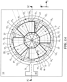
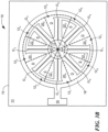
- a Field Effect Transistor (FET) 10 is shown here formed using photo-lithographic chemical etching processing. More particularly, the FET 10 includes a plurality of, here eight, FET cells 12 1 -12 8 , ( FIG. 3A ) interconnected by eight air bridges 11 1 -11 8 and controlled by a corresponding one of eight gates G 1 -G 8 , respectively ( FIGS. 2 and 3A ; FIG. 3B showing the FET 10 with the air bridges 11 1 -11 8 removed to more clearly show the cells 12 1 -12 8 ).
- Each one of the FET cells 12 1 -12 8 has, on an upper, planar surface 13 of a semiconductor substrate 15, here for example a substrate having gallium nitride (GaN), a corresponding one of eight gates G 1 -G 8 , respectively, in Schottky contact with the surface 13 of the semiconductor substrate 15, as shown in FIG. 1 ; each one of the eight gates G 1 -G 8 being disposed between a source (S) and a drain (D) in a manner to be described in more detail hereinafter to control a flow of carriers along a channel between the source pad (S) and drain pad (D) of each one of the eight, FET cells 12 1 -12 8 .
- a semiconductor substrate 15 here for example a substrate having gallium nitride (GaN), a corresponding one of eight gates G 1 -G 8 , respectively, in Schottky contact with the surface 13 of the semiconductor substrate 15, as shown in FIG. 1 ; each one of the eight gates G 1 -G 8 being disposed between
- each one of the gates G 1 -G 8 is here an elongated, finger-like gate and extends radially outward from a central, circular shaped gate pad 17, as shown.
- the gate pad 17 is electrically connected to a gate contact 18, shown more clearly in FIG. 4 ) disposed on a bottom surface 19 (FIG. 2B) of the semiconductor substrate 17 through an electrically conductive gate via 21 disposed at the center of the gate pad 17 and passing vertically through the substrate 15 between the gate pad 17 and the gate contact 23 ( FIGS. 3C and 4 ).
- the elongated, finger-like gates G 1 -G 8 are regularly spaced about the outer periphery of the common gate pad 17.
- the finger-like gate electrodes G 1 -G 8 are electrically interconnected to successive, evenly spaced points, P, ( FIG. 3B ) along an outer edge of the common, circular shaped, gate pad 17.
- P points
- the here eight elongated, finger-like gates Gi-Gs are separated one from the other by here forty-five degrees.
- the FET 10 also includes a drain contact 16 disposed on the upper surface 13 of the substrate 15 and terminating in a circular ring-like structure 18 ( FIG. 4 ) having a plurality of, here four, radially inwardly extending projections 20 1 -20 4 regularly spaced about an outer, circumferential rim of the circular structure 18; each one of the projections 20 1 -20 4 is a drain pad in ohmic contacted with the surface 13 of the semiconductor substrate 15.
- Each one of the projections 20 1 -20 8 provides a drain (D) ( FIGS. 2 , 3A , 3B ) for a pair of adjacent FET cells 12 1 -12 8 , in a manner to be described in more detail hereinafter.
- the central axis of the circular structure 18 and the center of the circular, common pad 17 are co-axial and are disposed along a common vertical Z axis, such Z axis being perpendicular to the X-Y planar surface 13 ( FIG. 3B ).
- the surface 13 is in the X-Y plane and the common vertical axis is along the Z-axis.
- the projections 20 1 -20 4 are spaced one from another by ninety degrees. It is noted that the projections 20 1 -20 4 terminate a predetermined distance from the outer periphery of the common gate pad 17 ( FIG. 3B ).
- each one of the projections 20 1 -20 4 is disposed between every other adjacent pair of the finger-like gates G 1 -G 8 ; as shown most clearly in FIG. 3B .
- each one of the projections 20 1 - 20 4 provides two drains (D) for the FET 10, one radial positioned side region of the projection 20 1 - 20 4 providing a drain for one of the eight FET cells 12 1 -12 8 and the opposite radially positioned side region providing a drain for the adjacent one of the eight FET cells 12 1 -12 8 .
- projection 20 1 is disposed between gates G 2 and G 3 ; projection 20 2 is disposed between gates G 4 and G 5 ; projection 20 3 is disposed between gates G 6 and G 7 ; and projection 20 4 is disposed between gates G 8 and G 1 .
- one side region of projection 20 1 provides the drain for FET cell 12 2 while the opposite side region of projection 20 1 provides the drain for FET cell 12 3 ;
- one side region of projection 20 2 provides the drain for FET cell 12 4 while the opposite side region of projection 20 1 provides the drain for FET cell 12 5 ;
- one side region of projection 20 3 provides the drain for FET cell 12 6 while the opposite side region of projection 20 3 provides the drain for FET cell 12 7 ;
- one side region of projection 20 4 provides the drain for FET cell 18 2 while the opposite side region of projection 20 4 provides the drain for FET cell 12 1 .
- An annular structure 30 ( FIG. 4 ) having a center coaxial with both the gate pad 17 and the circular ring-like structure 18 (along the Z-axis) has four source pads 22 1 - 22 4 ( FIGS. 2 , 3A and 3B ) regularly spaced circumferentially about the annular structure 30; that is the source pads 22 1 - 22 4 are spaced one from the other by ninety degrees and are disposed on the upper surface 13 ( FIGS. 2 , 3A and 3B ). Each one of the source pads 22 1 - 22 4 is in ohmic contacted with the surface 13 of the semiconductor substrate 15.
- the source pads 22 1 - 22 4 ( FIG. 4 ) are electrically interconnected by the air bridges 11 1 -11 4 ( FIGS.
- each one of the air bridges 11 1 -11 4 is elevated from the surface 13 and, more particularly, each one of the air bridges 11 1 -11 4 is elevated from a corresponding one of the projections 20 1 -20 4 and over a pair of adj acent Gi-Gs on each side of the such corresponding one of the projections; one gate finger on either side of the projection 20 1 -20 4 .
- air bridge 11 1 is over projection 20 1 and over gate fingers G 2 and G 3 ; air bridge 11 2 is over projection 20 2 and over gate fingers G 4 and G 5 ; air bridge 11 3 is over projection 20 3 and over gate fingers G 6 and G 7 ; and air bridge 11 4 is over projection 20 4 and over gate fingers G 8 and G 1 ; as indicated in FIGS. 2 and 3B .
- each one of the four source pads 22 1 - 22 4 is disposed between an adjacent pair of the finger-like gates G 1 -G 8 .
- source pad 22 1 is disposed between gates G 1 and G 2 ; source pad 22 2 is disposed between gates G 3 and G 4 ; source pad 22 3 is disposed between gates G 5 and G 6 ; and source pad 22 4 is disposed between gates G 7 and G 8 as shown in FIG. 3B .
- each one of the source pads 22 1 - 22 4 provides two sources (S) for the FET 10, one radial positioned side region of the source pad 22 1 - 22 4 providing a source (S) for one of the eight FET cells 12 1 -12s and the opposite radially positioned side region providing a source (S) for the adjacent one of the eight FET cells 12 1 -12 8 .
- each one of the gate fingers G 1 -G 8 is disposed between a source (S) and drain (D), with each one of the fingers Gi-Gs being adjacent one side of one of the source (S) and one side of the drain (D) while an adjacent one of the gate fingers G 1 -G 8 is adjacent the other side of the same drain (D) and one of the source (S). It follows then that each gate finger (G) shares a drain (D) provided by one of the projections or drain pads 20 1 -20 4 and a source (S) provided by an adjacent one of the source pads22 1 - 22 4 .
- a source contact 25, here provided by an electrical conductor 25 on the bottom surface 19 of the substrate 17 is electrically connected to the sources pads 22 1 -22 4 of the FET cells 12 1 -14 8 through, here four vias 27 ( FIGS. 2 , 3A and 4 ) passing vertically through the substrate 15 between the conductor 25 and the four source pads 22 1 -22 4 .
- a conductive feed 32 ( FIG. 4 ) for the gate pad 17.
- the feed 32 is a strip conductor 34 terminating in the gate contact 23.
- the gate contact 23 is connected to the gate pad 17 with a gate via 21.
- the gate via 21 is disposed within a circular array of the vias 27 thus forming a vertical quasi coaxial transmission line.
- the electrical conductor 25 ( FIG. 4 ) and feed 32 are electrically insulated from each other by the portion of the substrate 19 in the space between the feed 32 and the electrical conductor 25, as indicated.
- the conductor 25 on the bottom of the substrate 15 is spaced a predetermined distance from the feed line 34, as indicated, to provide a coplanar waveguide (CPW) transmission line feed for the 32.
- CPW coplanar waveguide
- the FET cells 12 1 -12 8 are disposed in an X-Y plane in a closed loop configuration, here for example, a circular configuration in the X-Y plane ( Fig. 3A and 3B ) on the upper surface 13 of the substrate 19.
- the FET 10 is suitable for flip chip mounting to a printed circuit board.
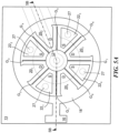
- the FET 10' has the air bridges 11 1 -11 4 eliminated since each one of the source pads 22 1 -22 4 is connected to ground conductor 25 of the bottom of the substrate 15 with the vias 27. More particularly, it was recognized that because the gates G1-G8 extend radially out from the pad 17, the source pads 22 1 -22 4 are triangular shaped and thus flare out from the center of the pad 17, there is now sufficient space towards the base of the triangle for placement of a via 27 thus eliminating the need for air bridges. To put it another way, the gate to gate spacing spreads out as one moves away from the center of the FET which allows for vias 27 for each source pad without growing the size of the FET.
- the FET 10' again includes the plurality of, here eight, FET cells 12 1 -12 8 , ( FIG. 3A ); here, however they are interconnected by the electrical conductor 25 through the vias 27. More particularly, as described above and shown more clearly in FIG 3B , one side region of projection 20 1 provides the drain for FET cell 12 2 while the opposite side region of projection 20 1 provides the drain for FET cell 12 3 ; one side region of projection 20 2 provides the drain for FET cell 12 4 while the opposite side region of projection 20 1 provides the drain for FET cell 12 5 ; one side region of projection 20 3 provides the drain for FET cell 12 6 while the opposite side region of projection 20 3 provides the drain for FET cell 12 7 ; and one side region of projection 20 4 provides the drain for FET cell 18 2 while the opposite side region of projection 20 4 provides the drain for FET cell 12 1 .
- the drain / RF output can be bonded to from the topside of this circular FET as shown in FIG. 5A .
- the FET 10' mounted to a printed circuit board 30 having an input impedance matching network (IMN) and an output impedance matching network (OMN) coupled to the FET 10'.
- the IMN is coupled to the gate contact 23 through a microstrip transmission line having a strip conductor 36 separated from a ground plane conductor 38.
- the strip conductor 36 is connected to the strip conductor 34 ( FIG. 4 ).
- the OMN is coupled to the drain contact 16 through a conductor 38 connecting the strip conductor 40 of a microstrip transmission line separated from an underlying portion of the ground plane conductor 38.
- a Field Effect Transistor includes: a plurality of FET cells having a plurality of source pads, a plurality of drain pads, and a plurality of gate electrodes disposed on a surface of a substrate, each one of the FET cells having a corresponding one of the gate electrodes disposed between one of the source pads and one of the drain pads, a gate contact connected to the gate electrode of each one of the FET cells, a drain contact connected to the drain pad of each one of the FET cells and a source contact connected to source pad of each one of the FET cells; wherein the cells are disposed in a loop configuration.
- the FET may include one or more of the following features, independently or in combination with another feature, to include: a gate pad disposed on an upper surface of the substrate connected to the plurality of gate electrodes wherein the gate contact is disposed on an bottom surface of the substrate; and wherein an electrically conductive gate via passes through the substrate to electrically connect the gate contact to the gate pad; wherein the gate pad is disposed in an inner region of the loop; wherein the gate electrodes projects outwardly from the gate pad; wherein one of the source contact or the drain contact is disposed on the bottom surface of the substrate; wherein one of the source contact or the drain contact is a conductor disposed on the bottom surface of the substrate and is connected to the corresponding one of the source pad or drain pad of each one of the FET cells though a corresponding one of a plurality of electrically conductive vias passing through the substrate; a strip conductor disposed on the bottom of the substrate, the feed line having one end connected to the gate contact through a gate via passing through the substrate, the feed line being spaced from
- a Field Effect Transistor includes: a plurality of FET cells having a plurality of source pads, a plurality of drain pads, and a plurality of gate electrodes disposed on a surface of a substrate; each one of the FET cells having a corresponding one of the gate electrodes disposed between one of the source pads and one of the drain pads; a gate contact connected to the gate electrodes of each one of the FET cells; a drain contact connected to the drain pad of each one of the FET cells; and a source contact connected to source pad of each one of the FET cells wherein the gate electrode of each one of the plurality of FET cells projects radially outwardly from a center of the FET.
- the FET may include one or more of the following features, independently or in combination with another feature, to include: wherein one of the source pads or drain pads of each one of the FET cells in the plurality of FET cells is connected to a contact on a bottom surface of the substrate through a corresponding one of a plurality of vias passing through the substrate, and wherein each one of the plurality of vias is disposed between a pair of the gates; a strip conductor disposed on the bottom of the substrate, the feed line having one end connected to the gate contact through a gate via passing through the substrate, the feed line being spaced from the conductor disposed on the bottom surface of the substrate; wherein the strip conductor and the conductor disposed on the bottom surface of the substrate provide a coplanar waveguide transmission line; wherein the gate via and the plurality of vias provide a quasi-coaxial transmission line.
Landscapes
- Junction Field-Effect Transistors (AREA)
Applications Claiming Priority (3)
| Application Number | Priority Date | Filing Date | Title |
|---|---|---|---|
| US14/830,148 US9698144B2 (en) | 2015-08-19 | 2015-08-19 | Field effect transistor having loop distributed field effect transistor cells |
| PCT/US2016/046106 WO2017030825A1 (en) | 2015-08-19 | 2016-08-09 | Field effect transistor having loop distributed field effect transistor cells |
| EP16757402.9A EP3338308B1 (de) | 2015-08-19 | 2016-08-09 | Feldeffekttransistor mit ringverteilten feldeffekttransistorzellen |
Related Parent Applications (2)
| Application Number | Title | Priority Date | Filing Date |
|---|---|---|---|
| EP16757402.9A Division-Into EP3338308B1 (de) | 2015-08-19 | 2016-08-09 | Feldeffekttransistor mit ringverteilten feldeffekttransistorzellen |
| EP16757402.9A Division EP3338308B1 (de) | 2015-08-19 | 2016-08-09 | Feldeffekttransistor mit ringverteilten feldeffekttransistorzellen |
Publications (2)
| Publication Number | Publication Date |
|---|---|
| EP4565032A2 true EP4565032A2 (de) | 2025-06-04 |
| EP4565032A3 EP4565032A3 (de) | 2025-08-27 |
Family
ID=56801790
Family Applications (2)
| Application Number | Title | Priority Date | Filing Date |
|---|---|---|---|
| EP25162449.0A Pending EP4565032A3 (de) | 2015-08-19 | 2016-08-09 | Feldeffekttransistor mit ringverteilten feldeffekttransistorzellen |
| EP16757402.9A Active EP3338308B1 (de) | 2015-08-19 | 2016-08-09 | Feldeffekttransistor mit ringverteilten feldeffekttransistorzellen |
Family Applications After (1)
| Application Number | Title | Priority Date | Filing Date |
|---|---|---|---|
| EP16757402.9A Active EP3338308B1 (de) | 2015-08-19 | 2016-08-09 | Feldeffekttransistor mit ringverteilten feldeffekttransistorzellen |
Country Status (5)
| Country | Link |
|---|---|
| US (1) | US9698144B2 (de) |
| EP (2) | EP4565032A3 (de) |
| JP (1) | JP6640330B2 (de) |
| CN (1) | CN107924937B (de) |
| WO (1) | WO2017030825A1 (de) |
Families Citing this family (2)
| Publication number | Priority date | Publication date | Assignee | Title |
|---|---|---|---|---|
| US10847428B2 (en) * | 2019-03-25 | 2020-11-24 | Istanbul Teknik Universitesi | CMOS compatible device based on four-terminal switching lattices |
| EP4607590A1 (de) * | 2024-02-26 | 2025-08-27 | NXP USA, Inc. | Ringbasierte anpassungsnetzwerke und verfahren |
Family Cites Families (22)
| Publication number | Priority date | Publication date | Assignee | Title |
|---|---|---|---|---|
| US3969745A (en) | 1974-09-18 | 1976-07-13 | Texas Instruments Incorporated | Interconnection in multi element planar structures |
| DE2603032A1 (de) | 1976-01-28 | 1977-08-11 | Licentia Gmbh | Vielfach-transistor |
| IT8048031A0 (it) * | 1979-04-09 | 1980-02-28 | Raytheon Co | Perfezionamento nei dispositivi a semiconduttore ad effetto di campo |
| US4315272A (en) | 1979-05-21 | 1982-02-09 | Raytheon Company | Field effect transistor |
| JPH0239573A (ja) * | 1988-07-29 | 1990-02-08 | Hitachi Ltd | ゲートバイアホール型半導体素子 |
| JPH0831606B2 (ja) * | 1989-11-17 | 1996-03-27 | 株式会社東芝 | 大電力用半導体装置 |
| JPH04171734A (ja) | 1990-11-02 | 1992-06-18 | Mitsubishi Electric Corp | 半導体装置 |
| JPH06232180A (ja) * | 1993-02-05 | 1994-08-19 | Nec Corp | 半導体装置 |
| US5539232A (en) * | 1994-05-31 | 1996-07-23 | Kabushiki Kaisha Toshiba | MOS composite type semiconductor device |
| JP3655947B2 (ja) | 1995-07-19 | 2005-06-02 | パイオニア株式会社 | 面放電型プラズマディスプレイパネル |
| JP3189691B2 (ja) | 1996-07-10 | 2001-07-16 | 株式会社村田製作所 | 高周波半導体デバイス |
| US6140687A (en) * | 1996-11-28 | 2000-10-31 | Matsushita Electric Industrial Co., Ltd. | High frequency ring gate MOSFET |
| JP3129223B2 (ja) * | 1997-02-28 | 2001-01-29 | 日本電気株式会社 | 半導体装置 |
| EP1060517A1 (de) * | 1998-02-27 | 2000-12-20 | ABB Semiconductors AG | Bipolartransistor mit isolierter gateelektrode |
| DE10261457B3 (de) | 2002-12-31 | 2004-03-25 | Infineon Technologies Ag | Integrierte Schaltungsanordnung mit einem Transistorarray aus vertikalen FET-Auswahltransistoren |
| JP4912621B2 (ja) | 2005-06-07 | 2012-04-11 | 富士通株式会社 | 半導体装置及び半導体装置の配線方法 |
| JP2010165789A (ja) * | 2009-01-14 | 2010-07-29 | Panasonic Corp | 半導体集積回路およびその製造方法 |
| US8183639B2 (en) | 2010-10-07 | 2012-05-22 | Freescale Semiconductor, Inc. | Dual port static random access memory cell layout |
| US8724393B2 (en) | 2011-05-02 | 2014-05-13 | Macronix International Co., Ltd. | Thermally assisted flash memory with diode strapping |
| US8723268B2 (en) | 2012-06-13 | 2014-05-13 | Synopsys, Inc. | N-channel and P-channel end-to-end finFET cell architecture with relaxed gate pitch |
| US8816397B2 (en) | 2012-12-21 | 2014-08-26 | The United States Of America As Represented By The Secretary Of The Army | Ring-shaped transistors providing reduced self-heating |
| US9331154B2 (en) | 2013-08-21 | 2016-05-03 | Epistar Corporation | High electron mobility transistor |
-
2015
- 2015-08-19 US US14/830,148 patent/US9698144B2/en active Active
-
2016
- 2016-08-09 EP EP25162449.0A patent/EP4565032A3/de active Pending
- 2016-08-09 CN CN201680048556.5A patent/CN107924937B/zh active Active
- 2016-08-09 JP JP2018508692A patent/JP6640330B2/ja active Active
- 2016-08-09 WO PCT/US2016/046106 patent/WO2017030825A1/en not_active Ceased
- 2016-08-09 EP EP16757402.9A patent/EP3338308B1/de active Active
Also Published As
| Publication number | Publication date |
|---|---|
| CN107924937A (zh) | 2018-04-17 |
| CN107924937B (zh) | 2021-06-15 |
| JP2018528611A (ja) | 2018-09-27 |
| WO2017030825A1 (en) | 2017-02-23 |
| EP3338308B1 (de) | 2025-06-04 |
| EP4565032A3 (de) | 2025-08-27 |
| US9698144B2 (en) | 2017-07-04 |
| US20170053910A1 (en) | 2017-02-23 |
| JP6640330B2 (ja) | 2020-02-05 |
| EP3338308A1 (de) | 2018-06-27 |
Similar Documents
| Publication | Publication Date | Title |
|---|---|---|
| US10014321B2 (en) | Radio-frequency switches having silicon-on-insulator field-effect transistors with reduced linear region resistance | |
| US9685438B2 (en) | Field effect transistor having two-dimensionally distributed field effect transistor cells | |
| KR20090042739A (ko) | 반도체 장치 | |
| JP6949115B2 (ja) | 半導体デバイス及びその製造方法 | |
| EP2838194B1 (de) | Verstärkerschaltungen | |
| KR20070012792A (ko) | 열 스페이서를 갖는 반도체 소자 | |
| CN109585561B (zh) | 具有漏极通孔布置的晶体管管芯以及其制造方法 | |
| US6081006A (en) | Reduced size field effect transistor | |
| TWI836127B (zh) | 場效電晶體之佈局優化 | |
| US4107720A (en) | Overlay metallization multi-channel high frequency field effect transistor | |
| CN115485827A (zh) | 具有共享电极的集成晶体管 | |
| KR20200062938A (ko) | 스택된 전계효과트랜지스터(fet)를 갖는 반도체 디바이스 | |
| EP4565032A2 (de) | Feldeffekttransistor mit ringverteilten feldeffekttransistorzellen | |
| US8816397B2 (en) | Ring-shaped transistors providing reduced self-heating | |
| KR102081497B1 (ko) | 고출력 rf 트랜지스터 상의 매립형 고조파 종단 | |
| US20240347485A1 (en) | Microwave integrated circuit and manufacturing method of the same | |
| US8963658B2 (en) | Micropstrip transmission line/coplanar waveguide (CPW) transistor structure | |
| US9472497B2 (en) | Semiconductor device | |
| CN105743451B (zh) | 一种射频功率放大器版图及射频功率放大器 | |
| US20160329420A1 (en) | Field Effect Transistor Structure Having Notched Mesa | |
| KR102752888B1 (ko) | 선택 가능한 입출력 포트를 구비한 복수개의 전력 결합 증폭기를 포함하는 반도체 소자 | |
| JPH09232334A (ja) | 化合物半導体装置 | |
| CN118366972A (zh) | 一种无线射频元件 | |
| CN104899343A (zh) | 交叉栅结构mosfet及多叉指栅结构mosfet的版图设计 |
Legal Events
| Date | Code | Title | Description |
|---|---|---|---|
| PUAI | Public reference made under article 153(3) epc to a published international application that has entered the european phase |
Free format text: ORIGINAL CODE: 0009012 |
|
| STAA | Information on the status of an ep patent application or granted ep patent |
Free format text: STATUS: REQUEST FOR EXAMINATION WAS MADE |
|
| 17P | Request for examination filed |
Effective date: 20250307 |
|
| AC | Divisional application: reference to earlier application |
Ref document number: 3338308 Country of ref document: EP Kind code of ref document: P |
|
| AK | Designated contracting states |
Kind code of ref document: A2 Designated state(s): AL AT BE BG CH CY CZ DE DK EE ES FI FR GB GR HR HU IE IS IT LI LT LU LV MC MK MT NL NO PL PT RO RS SE SI SK SM TR |
|
| REG | Reference to a national code |
Ref country code: DE Ref legal event code: R079 Free format text: PREVIOUS MAIN CLASS: H10D0064270000 Ipc: H01L0023660000 |
|
| PUAL | Search report despatched |
Free format text: ORIGINAL CODE: 0009013 |
|
| AK | Designated contracting states |
Kind code of ref document: A3 Designated state(s): AL AT BE BG CH CY CZ DE DK EE ES FI FR GB GR HR HU IE IS IT LI LT LU LV MC MK MT NL NO PL PT RO RS SE SI SK SM TR |
|
| RIC1 | Information provided on ipc code assigned before grant |
Ipc: H01L 23/66 20060101AFI20250718BHEP Ipc: H01L 23/48 20060101ALI20250718BHEP Ipc: H10D 30/87 20250101ALI20250718BHEP Ipc: H10D 64/23 20250101ALI20250718BHEP Ipc: H10D 64/27 20250101ALI20250718BHEP |