EP4531102A2 - Einbettung einer komponente mit vorverbundener säule in komponententräger - Google Patents
Einbettung einer komponente mit vorverbundener säule in komponententräger Download PDFInfo
- Publication number
- EP4531102A2 EP4531102A2 EP25158168.2A EP25158168A EP4531102A2 EP 4531102 A2 EP4531102 A2 EP 4531102A2 EP 25158168 A EP25158168 A EP 25158168A EP 4531102 A2 EP4531102 A2 EP 4531102A2
- Authority
- EP
- European Patent Office
- Prior art keywords
- component
- electrically conductive
- layer structure
- pillars
- insulating layer
- Prior art date
- Legal status (The legal status is an assumption and is not a legal conclusion. Google has not performed a legal analysis and makes no representation as to the accuracy of the status listed.)
- Pending
Links
Images








Classifications
-
- H—ELECTRICITY
- H05—ELECTRIC TECHNIQUES NOT OTHERWISE PROVIDED FOR
- H05K—PRINTED CIRCUITS; CASINGS OR CONSTRUCTIONAL DETAILS OF ELECTRIC APPARATUS; MANUFACTURE OF ASSEMBLAGES OF ELECTRICAL COMPONENTS
- H05K1/00—Printed circuits
- H05K1/18—Printed circuits structurally associated with non-printed electric components
- H05K1/182—Printed circuits structurally associated with non-printed electric components associated with components mounted in printed circuit boards [PCB], e.g. insert-mounted components [IMC]
- H05K1/185—Printed circuits structurally associated with non-printed electric components associated with components mounted in printed circuit boards [PCB], e.g. insert-mounted components [IMC] associated with components encapsulated in the insulating substrate of the PCBs; associated with components incorporated in internal layers of multilayer circuit boards
- H05K1/188—Printed circuits structurally associated with non-printed electric components associated with components mounted in printed circuit boards [PCB], e.g. insert-mounted components [IMC] associated with components encapsulated in the insulating substrate of the PCBs; associated with components incorporated in internal layers of multilayer circuit boards manufactured by mounting on or attaching to a structure having a conductive layer, e.g. a metal foil, such that the terminals of the component are connected to or adjacent to the conductive layer before embedding, and by using the conductive layer, which is patterned after embedding, at least partially for connecting the component
-
- H—ELECTRICITY
- H05—ELECTRIC TECHNIQUES NOT OTHERWISE PROVIDED FOR
- H05K—PRINTED CIRCUITS; CASINGS OR CONSTRUCTIONAL DETAILS OF ELECTRIC APPARATUS; MANUFACTURE OF ASSEMBLAGES OF ELECTRICAL COMPONENTS
- H05K3/00—Apparatus or processes for manufacturing printed circuits
- H05K3/40—Forming printed elements for providing electric connections to or between printed circuits
- H05K3/42—Plated through-holes or plated via connections
-
- H—ELECTRICITY
- H05—ELECTRIC TECHNIQUES NOT OTHERWISE PROVIDED FOR
- H05K—PRINTED CIRCUITS; CASINGS OR CONSTRUCTIONAL DETAILS OF ELECTRIC APPARATUS; MANUFACTURE OF ASSEMBLAGES OF ELECTRICAL COMPONENTS
- H05K1/00—Printed circuits
- H05K1/02—Details
-
- H—ELECTRICITY
- H05—ELECTRIC TECHNIQUES NOT OTHERWISE PROVIDED FOR
- H05K—PRINTED CIRCUITS; CASINGS OR CONSTRUCTIONAL DETAILS OF ELECTRIC APPARATUS; MANUFACTURE OF ASSEMBLAGES OF ELECTRICAL COMPONENTS
- H05K1/00—Printed circuits
- H05K1/02—Details
- H05K1/11—Printed elements for providing electric connections to or between printed circuits
-
- H—ELECTRICITY
- H05—ELECTRIC TECHNIQUES NOT OTHERWISE PROVIDED FOR
- H05K—PRINTED CIRCUITS; CASINGS OR CONSTRUCTIONAL DETAILS OF ELECTRIC APPARATUS; MANUFACTURE OF ASSEMBLAGES OF ELECTRICAL COMPONENTS
- H05K1/00—Printed circuits
- H05K1/02—Details
- H05K1/11—Printed elements for providing electric connections to or between printed circuits
- H05K1/111—Pads for surface mounting, e.g. lay-out
-
- H—ELECTRICITY
- H05—ELECTRIC TECHNIQUES NOT OTHERWISE PROVIDED FOR
- H05K—PRINTED CIRCUITS; CASINGS OR CONSTRUCTIONAL DETAILS OF ELECTRIC APPARATUS; MANUFACTURE OF ASSEMBLAGES OF ELECTRICAL COMPONENTS
- H05K1/00—Printed circuits
- H05K1/18—Printed circuits structurally associated with non-printed electric components
- H05K1/182—Printed circuits structurally associated with non-printed electric components associated with components mounted in printed circuit boards [PCB], e.g. insert-mounted components [IMC]
- H05K1/185—Printed circuits structurally associated with non-printed electric components associated with components mounted in printed circuit boards [PCB], e.g. insert-mounted components [IMC] associated with components encapsulated in the insulating substrate of the PCBs; associated with components incorporated in internal layers of multilayer circuit boards
-
- H—ELECTRICITY
- H05—ELECTRIC TECHNIQUES NOT OTHERWISE PROVIDED FOR
- H05K—PRINTED CIRCUITS; CASINGS OR CONSTRUCTIONAL DETAILS OF ELECTRIC APPARATUS; MANUFACTURE OF ASSEMBLAGES OF ELECTRICAL COMPONENTS
- H05K3/00—Apparatus or processes for manufacturing printed circuits
- H05K3/0011—Working of insulating substrates or insulating layers
-
- H—ELECTRICITY
- H05—ELECTRIC TECHNIQUES NOT OTHERWISE PROVIDED FOR
- H05K—PRINTED CIRCUITS; CASINGS OR CONSTRUCTIONAL DETAILS OF ELECTRIC APPARATUS; MANUFACTURE OF ASSEMBLAGES OF ELECTRICAL COMPONENTS
- H05K3/00—Apparatus or processes for manufacturing printed circuits
- H05K3/007—Manufacture or processing of a substrate for a printed circuit board supported by a temporary or sacrificial carrier
-
- H—ELECTRICITY
- H05—ELECTRIC TECHNIQUES NOT OTHERWISE PROVIDED FOR
- H05K—PRINTED CIRCUITS; CASINGS OR CONSTRUCTIONAL DETAILS OF ELECTRIC APPARATUS; MANUFACTURE OF ASSEMBLAGES OF ELECTRICAL COMPONENTS
- H05K3/00—Apparatus or processes for manufacturing printed circuits
- H05K3/02—Apparatus or processes for manufacturing printed circuits in which the conductive material is applied to the surface of the insulating support and is thereafter removed from such areas of the surface which are not intended for current conducting or shielding
-
- H—ELECTRICITY
- H05—ELECTRIC TECHNIQUES NOT OTHERWISE PROVIDED FOR
- H05K—PRINTED CIRCUITS; CASINGS OR CONSTRUCTIONAL DETAILS OF ELECTRIC APPARATUS; MANUFACTURE OF ASSEMBLAGES OF ELECTRICAL COMPONENTS
- H05K3/00—Apparatus or processes for manufacturing printed circuits
- H05K3/30—Assembling printed circuits with electric components, e.g. with resistors
- H05K3/32—Assembling printed circuits with electric components, e.g. with resistors electrically connecting electric components or wires to printed circuits
- H05K3/34—Assembling printed circuits with electric components, e.g. with resistors electrically connecting electric components or wires to printed circuits by soldering
- H05K3/341—Surface mounted components
- H05K3/3431—Leadless components
- H05K3/3436—Leadless components having an array of bottom contacts, e.g. pad grid array or ball grid array components
-
- H—ELECTRICITY
- H05—ELECTRIC TECHNIQUES NOT OTHERWISE PROVIDED FOR
- H05K—PRINTED CIRCUITS; CASINGS OR CONSTRUCTIONAL DETAILS OF ELECTRIC APPARATUS; MANUFACTURE OF ASSEMBLAGES OF ELECTRICAL COMPONENTS
- H05K3/00—Apparatus or processes for manufacturing printed circuits
- H05K3/40—Forming printed elements for providing electric connections to or between printed circuits
-
- H—ELECTRICITY
- H05—ELECTRIC TECHNIQUES NOT OTHERWISE PROVIDED FOR
- H05K—PRINTED CIRCUITS; CASINGS OR CONSTRUCTIONAL DETAILS OF ELECTRIC APPARATUS; MANUFACTURE OF ASSEMBLAGES OF ELECTRICAL COMPONENTS
- H05K3/00—Apparatus or processes for manufacturing printed circuits
- H05K3/40—Forming printed elements for providing electric connections to or between printed circuits
- H05K3/4007—Surface contacts, e.g. bumps
-
- H—ELECTRICITY
- H05—ELECTRIC TECHNIQUES NOT OTHERWISE PROVIDED FOR
- H05K—PRINTED CIRCUITS; CASINGS OR CONSTRUCTIONAL DETAILS OF ELECTRIC APPARATUS; MANUFACTURE OF ASSEMBLAGES OF ELECTRICAL COMPONENTS
- H05K3/00—Apparatus or processes for manufacturing printed circuits
- H05K3/40—Forming printed elements for providing electric connections to or between printed circuits
- H05K3/4038—Through-connections; Vertical interconnect access [VIA] connections
-
- H—ELECTRICITY
- H10—SEMICONDUCTOR DEVICES; ELECTRIC SOLID-STATE DEVICES NOT OTHERWISE PROVIDED FOR
- H10W—GENERIC PACKAGES, INTERCONNECTIONS, CONNECTORS OR OTHER CONSTRUCTIONAL DETAILS OF DEVICES COVERED BY CLASS H10
- H10W70/00—Package substrates; Interposers; Redistribution layers [RDL]
- H10W70/01—Manufacture or treatment
- H10W70/05—Manufacture or treatment of insulating or insulated package substrates, or of interposers, or of redistribution layers
- H10W70/08—Manufacture or treatment of insulating or insulated package substrates, or of interposers, or of redistribution layers by depositing layers on the chip or wafer, e.g. "chip-first" RDLs
- H10W70/09—Manufacture or treatment of insulating or insulated package substrates, or of interposers, or of redistribution layers by depositing layers on the chip or wafer, e.g. "chip-first" RDLs extending onto an encapsulation that laterally surrounds the chip or wafer, e.g. fan-out wafer level package [FOWLP] RDLs
-
- H—ELECTRICITY
- H10—SEMICONDUCTOR DEVICES; ELECTRIC SOLID-STATE DEVICES NOT OTHERWISE PROVIDED FOR
- H10W—GENERIC PACKAGES, INTERCONNECTIONS, CONNECTORS OR OTHER CONSTRUCTIONAL DETAILS OF DEVICES COVERED BY CLASS H10
- H10W70/00—Package substrates; Interposers; Redistribution layers [RDL]
- H10W70/60—Insulating or insulated package substrates; Interposers; Redistribution layers
-
- H—ELECTRICITY
- H10—SEMICONDUCTOR DEVICES; ELECTRIC SOLID-STATE DEVICES NOT OTHERWISE PROVIDED FOR
- H10W—GENERIC PACKAGES, INTERCONNECTIONS, CONNECTORS OR OTHER CONSTRUCTIONAL DETAILS OF DEVICES COVERED BY CLASS H10
- H10W70/00—Package substrates; Interposers; Redistribution layers [RDL]
- H10W70/60—Insulating or insulated package substrates; Interposers; Redistribution layers
- H10W70/611—Insulating or insulated package substrates; Interposers; Redistribution layers for connecting multiple chips together
- H10W70/614—Insulating or insulated package substrates; Interposers; Redistribution layers for connecting multiple chips together the multiple chips being integrally enclosed
-
- H—ELECTRICITY
- H10—SEMICONDUCTOR DEVICES; ELECTRIC SOLID-STATE DEVICES NOT OTHERWISE PROVIDED FOR
- H10W—GENERIC PACKAGES, INTERCONNECTIONS, CONNECTORS OR OTHER CONSTRUCTIONAL DETAILS OF DEVICES COVERED BY CLASS H10
- H10W72/00—Interconnections or connectors in packages
- H10W72/01—Manufacture or treatment
- H10W72/0198—Manufacture or treatment batch processes
-
- H—ELECTRICITY
- H05—ELECTRIC TECHNIQUES NOT OTHERWISE PROVIDED FOR
- H05K—PRINTED CIRCUITS; CASINGS OR CONSTRUCTIONAL DETAILS OF ELECTRIC APPARATUS; MANUFACTURE OF ASSEMBLAGES OF ELECTRICAL COMPONENTS
- H05K2201/00—Indexing scheme relating to printed circuits covered by H05K1/00
- H05K2201/10—Details of components or other objects attached to or integrated in a printed circuit board
- H05K2201/10613—Details of electrical connections of non-printed components, e.g. special leads
- H05K2201/10621—Components characterised by their electrical contacts
- H05K2201/10704—Pin grid array [PGA]
-
- H—ELECTRICITY
- H05—ELECTRIC TECHNIQUES NOT OTHERWISE PROVIDED FOR
- H05K—PRINTED CIRCUITS; CASINGS OR CONSTRUCTIONAL DETAILS OF ELECTRIC APPARATUS; MANUFACTURE OF ASSEMBLAGES OF ELECTRICAL COMPONENTS
- H05K2201/00—Indexing scheme relating to printed circuits covered by H05K1/00
- H05K2201/10—Details of components or other objects attached to or integrated in a printed circuit board
- H05K2201/10613—Details of electrical connections of non-printed components, e.g. special leads
- H05K2201/10954—Other details of electrical connections
- H05K2201/10977—Encapsulated connections
-
- H—ELECTRICITY
- H05—ELECTRIC TECHNIQUES NOT OTHERWISE PROVIDED FOR
- H05K—PRINTED CIRCUITS; CASINGS OR CONSTRUCTIONAL DETAILS OF ELECTRIC APPARATUS; MANUFACTURE OF ASSEMBLAGES OF ELECTRICAL COMPONENTS
- H05K2201/00—Indexing scheme relating to printed circuits covered by H05K1/00
- H05K2201/10—Details of components or other objects attached to or integrated in a printed circuit board
- H05K2201/10613—Details of electrical connections of non-printed components, e.g. special leads
- H05K2201/10954—Other details of electrical connections
- H05K2201/10984—Component carrying a connection agent, e.g. solder, adhesive
-
- H—ELECTRICITY
- H05—ELECTRIC TECHNIQUES NOT OTHERWISE PROVIDED FOR
- H05K—PRINTED CIRCUITS; CASINGS OR CONSTRUCTIONAL DETAILS OF ELECTRIC APPARATUS; MANUFACTURE OF ASSEMBLAGES OF ELECTRICAL COMPONENTS
- H05K2201/00—Indexing scheme relating to printed circuits covered by H05K1/00
- H05K2201/10—Details of components or other objects attached to or integrated in a printed circuit board
- H05K2201/10613—Details of electrical connections of non-printed components, e.g. special leads
- H05K2201/10954—Other details of electrical connections
- H05K2201/10992—Using different connection materials, e.g. different solders, for the same connection
-
- H—ELECTRICITY
- H05—ELECTRIC TECHNIQUES NOT OTHERWISE PROVIDED FOR
- H05K—PRINTED CIRCUITS; CASINGS OR CONSTRUCTIONAL DETAILS OF ELECTRIC APPARATUS; MANUFACTURE OF ASSEMBLAGES OF ELECTRICAL COMPONENTS
- H05K2203/00—Indexing scheme relating to apparatus or processes for manufacturing printed circuits covered by H05K3/00
- H05K2203/02—Details related to mechanical or acoustic processing, e.g. drilling, punching, cutting, using ultrasound
- H05K2203/0278—Flat pressure, e.g. for connecting terminals with anisotropic conductive adhesive
-
- H—ELECTRICITY
- H05—ELECTRIC TECHNIQUES NOT OTHERWISE PROVIDED FOR
- H05K—PRINTED CIRCUITS; CASINGS OR CONSTRUCTIONAL DETAILS OF ELECTRIC APPARATUS; MANUFACTURE OF ASSEMBLAGES OF ELECTRICAL COMPONENTS
- H05K2203/00—Indexing scheme relating to apparatus or processes for manufacturing printed circuits covered by H05K3/00
- H05K2203/11—Treatments characterised by their effect, e.g. heating, cooling, roughening
- H05K2203/1189—Pressing leads, bumps or a die through an insulating layer
-
- H—ELECTRICITY
- H10—SEMICONDUCTOR DEVICES; ELECTRIC SOLID-STATE DEVICES NOT OTHERWISE PROVIDED FOR
- H10W—GENERIC PACKAGES, INTERCONNECTIONS, CONNECTORS OR OTHER CONSTRUCTIONAL DETAILS OF DEVICES COVERED BY CLASS H10
- H10W70/00—Package substrates; Interposers; Redistribution layers [RDL]
- H10W70/099—Connecting interconnections to insulating or insulated package substrates, interposers or redistribution layers
-
- H—ELECTRICITY
- H10—SEMICONDUCTOR DEVICES; ELECTRIC SOLID-STATE DEVICES NOT OTHERWISE PROVIDED FOR
- H10W—GENERIC PACKAGES, INTERCONNECTIONS, CONNECTORS OR OTHER CONSTRUCTIONAL DETAILS OF DEVICES COVERED BY CLASS H10
- H10W72/00—Interconnections or connectors in packages
- H10W72/071—Connecting or disconnecting
- H10W72/073—Connecting or disconnecting of die-attach connectors
-
- H—ELECTRICITY
- H10—SEMICONDUCTOR DEVICES; ELECTRIC SOLID-STATE DEVICES NOT OTHERWISE PROVIDED FOR
- H10W—GENERIC PACKAGES, INTERCONNECTIONS, CONNECTORS OR OTHER CONSTRUCTIONAL DETAILS OF DEVICES COVERED BY CLASS H10
- H10W72/00—Interconnections or connectors in packages
- H10W72/851—Dispositions of multiple connectors or interconnections
- H10W72/874—On different surfaces
-
- H—ELECTRICITY
- H10—SEMICONDUCTOR DEVICES; ELECTRIC SOLID-STATE DEVICES NOT OTHERWISE PROVIDED FOR
- H10W—GENERIC PACKAGES, INTERCONNECTIONS, CONNECTORS OR OTHER CONSTRUCTIONAL DETAILS OF DEVICES COVERED BY CLASS H10
- H10W72/00—Interconnections or connectors in packages
- H10W72/90—Bond pads, in general
- H10W72/941—Dispositions of bond pads
- H10W72/9413—Dispositions of bond pads on encapsulations
-
- H—ELECTRICITY
- H10—SEMICONDUCTOR DEVICES; ELECTRIC SOLID-STATE DEVICES NOT OTHERWISE PROVIDED FOR
- H10W—GENERIC PACKAGES, INTERCONNECTIONS, CONNECTORS OR OTHER CONSTRUCTIONAL DETAILS OF DEVICES COVERED BY CLASS H10
- H10W74/00—Encapsulations, e.g. protective coatings
- H10W74/10—Encapsulations, e.g. protective coatings characterised by their shape or disposition
- H10W74/131—Encapsulations, e.g. protective coatings characterised by their shape or disposition the semiconductor body being only partially enclosed
- H10W74/142—Encapsulations, e.g. protective coatings characterised by their shape or disposition the semiconductor body being only partially enclosed the encapsulations exposing the passive side of the semiconductor body
Definitions
- the invention relates to a method of manufacturing a component carrier, and to component carriers.
- component carriers equipped with one or more electronic components and increasing miniaturization of such electronic components as well as a rising number of electronic components to be mounted on the component carriers such as printed circuit boards
- increasingly more powerful array-like components or packages having several electronic components are being employed, which have a plurality of contacts or connections, with ever smaller spacing between these contacts. Removal of heat generated by such electronic components and the component carrier itself during operation also becomes an increasing issue.
- component carriers shall be mechanically robust and electrically reliable so as to be operable even under harsh conditions.
- US 2014/201992 A1 discloses a method for fabricating a circuit board structure having at least an embedded electronic element, which includes the steps of providing a substrate and embedding at least an electronic element in the substrate with an active surface and a plurality of electrode pads of the electronic element exposed from a surface of the substrate, forming a plurality of conductive bumps on the electrode pads of the electronic element, and covering the surface of the substrate and the active surface of the electronic element with a dielectric layer and a metal layer stacked on the dielectric layer, wherein the conductive bumps penetrate the dielectric layer so as to be in contact with the metal layer.
- TW 200715930 discloses a method for manufacturing a substrate embedded with an electronic device.
- An electronic component having a plurality of electrodes is disposed in a cavity of a core plate.
- at least a metal foil is pressed on the core plate and the electronic component, such that the metal foil is electrically connected with the electrodes of the electronic component.
- the metal foil is patterned to have a plurality of contacts.
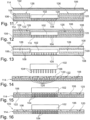
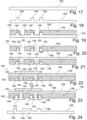
- a method of manufacturing a component carrier comprises galvanically depositing at least part of at least one electrically conductive pillar on a component, and inserting (and optionally fixing) the at least one electrically conductive pillar and an electrically insulating layer structure into one another. Thereby, at least part of an embedding procedure may be accomplished.
- a component carrier comprising a carrier body having a cavity and comprising at least one electrically conductive layer structure at least partially forming a surface of the carrier body, a component with at least one connected electrically conductive pillar, wherein the component is arranged at least partially in the cavity, and an electrically insulating layer structure in which the at least one electrically conductive pillar is at least partially inserted so that the at least one electrically conductive pillar extends vertically beyond the at least one electrically conductive layer structure.
- a component carrier comprising a component with at least one connected cylindrical electrically conductive pillar, and an electrically insulating layer structure in which the at least one electrically conductive pillar is at least partially inserted and fixed.
- component carrier may particularly denote any support structure which is capable of accommodating one or more components thereon and/or therein for providing mechanical support and/or electrical connectivity.
- a component carrier may be configured as a mechanical and/or electronic carrier for components.
- a component carrier may be one of a printed circuit board, an organic interposer, and an IC (integrated circuit) substrate.
- a component carrier may also be a hybrid board combining different ones of the above mentioned types of component carriers.
- pillar may particularly denote a tiny post extending from the component and being oriented preferably substantially perpendicular to a main surface of the component.
- a pillar may be a lengthy structure extending in a pin-like or even spike-like way from the component.
- the aspect ratio can be defined as the ratio between a length and a diameter of the pillar.
- the term "galvanically depositing” may particularly denote a manufacturing process of the pillar according to which the material of the pillar is at least partially deposited on or above a surface of the component or a pre-form thereof (in particular a wafer comprising multiple such components) by electroplating, in particular in an additive or semi-additive process.
- the component or pre-form thereof may be immersed in a solution from which material solidifies on the component to thereby form the corresponding pillar or part of the pillar.
- Such a manufacturing process of forming at least part of the pillar may involve a lithographic procedure during which a surface of the component or pre-form thereof may be covered with a patterned photoresist or the like to thereby define one or more surface portions of the component where one or more pillars may be galvanically deposited.
- a metal such as copper
- water based solutions for instance electrolytes
- An electric field between an anode and a work piece (such as the component with one or more pads or a pre-form thereof, for instance a wafer integrally connecting multiple such components with pads) as cathode may force positively charged metal ions to move to the cathode where they give up their charge and deposit themselves as metal on the surface of the work piece.
- Electroplating or galvanic deposition processes may encompass, besides the pure metal deposition, also preparative and/or post treatments of the component(s) to be coated.
- the term "cylindrical” may particularly denote that the pillar(s) may have a cross-sectional shape and area which remains substantially constant along the entire extension of the pillar from a main surface of the component up to a free end of the pillar.
- this cross-sectional may be circular with a constant radius along the extension of the respective pillar.
- a component carrier manufacturing procedure in which one or preferably multiple electrically conductive pillars are formed to extend from a main surface of a component, and extending substantially vertically thereto.
- Such pillars may be advantageously formed by a galvanic deposition process.
- Such a galvanic deposition process has the advantage that pillars may be formed simultaneously for multiple components even on a wafer level, i.e. in a configuration in which multiple pre-forms of components are still integrally connected in a wafer compound. This allows for a simple and an efficient production of the pillars with high robustness and small tolerance.
- an electrically insulating layer structure may be provided so that one or more pillars extend vertically into the dielectric layer structure and beyond an electrically conductive layer structure of a carrier body (such as a core with electrically conductive traces) in which the component is located.
- a carrier body such as a core with electrically conductive traces
- the at least one electrically conductive pillar comprises or consists of copper, in particular it may comprise a copper-titanium base portion and a copper top portion thereon.
- the component with pillar(s) is particularly appropriate for component carrier technology such as PCB (printed circuit board) technology which usually uses copper for electric connection purposes. Therefore, copper as top portion of the pillar is highly advantageous.
- a base portion specifically adapted for such a connection is highly advantageous.
- a pad of a component may comprise or consist of aluminum which can be properly connected with a copper-titanium base portion of the pillar.
- other materials and material combinations are possible as well.
- the method comprises providing the electrically insulating layer structure of an at least partially uncured material, and at least partially (preferably fulling) curing the at least partially uncured material of the electrically insulating layer structure during the inserting and fixing.
- at least partially uncured material particularly denotes material which has the property to at least partially melt or become flowable by the application of elevated pressure and/or elevated temperature, and become fully hardened or cured (and thereby becomes solid) when releasing the applied elevated pressure and/or elevated temperature. Consequently, applying elevated pressure and/or elevated temperature may cause melting of the curable or at least partially uncured material, followed by an irreversible hardening upon releasing the applied high pressure and/or high temperature.
- the "at least partially uncured material” may comprise or consist of B-stage material and/or A-stage material.
- the layer structure may re-melt during lamination so that resin (or the like) may flow for interconnecting the various elements and for closing gaps or voids and may therefore contribute to a stable intrinsic interconnection within the component carrier under manufacture. Therefore, the fixing between pillars with components on the one hand and the electrically insulating layer structure on the other hand may be carried out by lamination, i.e. the application of pressure and/or heat, which results in a curing of previously at least partially uncured material of the electrically insulating layer structure for accomplishing the fixing and contributing to the embedding.
- the electrically insulating layer structure may form part of the readily manufactured component carrier.
- the method comprises drilling (in particular by at least one of laser drilling and mechanically drilling) at least one hole through at least one of the electrically insulating layer structure and the at least one further electrically insulating layer structure. It is further possible to at least partially fill the at least one drilled hole with electrically conductive material (for instance by plating) to thereby contact the at least one electrically conductive pillar and/or directly the component.
- electrically conductive material for instance by plating
- a connection between different pillars may be accomplished by drilling a hole and filling the latter with electrically conductive material (in particular copper), for instance by plating.
- electrically conductive material in particular copper
- the method comprises attaching a carrier to the electrically insulating layer structure prior to the inserting.
- a carrier may be a temporary carrier, i.e. may be later removed before completing manufacture of the component carrier.
- a temporary carrier does not form part of the readily manufactured component carrier.
- the carrier providing mechanical support during inserting and fixing may remain as part of the component carrier and may therefore form part thereof. It is also possible that only part of the carrier is later removed, and a remaining portion forms part of the final component carrier.
- the method comprises removing at least part of the attached carrier from the electrically insulating layer structure after to the inserting.
- the carrier is a temporary carrier, it may be removed completely after inserting (and preferably fixing), when the presence of the temporary carrier for providing mechanical support is no longer needed.
- Such a need of a temporary carrier for providing mechanical support may exit no longer when the constituents of the component carrier itself have become mechanically sufficiently stable to provide support and avoid undesired effects such as warpage. For instance, curing an at least partially uncured material of the at least one electrically insulating layer structure may result in a hardening of the obtained structure and may render the presence of the temporary carrier for the further processing dispensable.
- the carrier comprises a core, or a core covered with at least one electrically conductive layer structure, or a thinner electrically conductive layer on a thicker electrically conductive layer, or a plastic layer (in particular a polyethylene terephthalate layer).
- the carrier may be flexible, for instance may comprise or consist of a sticky tape. It is however also possible that the carrier is mechanically stiff, for instance a fully cured core (for instance of FR4 material). Also the provision of the carrier as a stack of multiple electrically conductive layer structures (in particular of highly different thickness) which can be delaminated from one another selectively is an option.
- a part of the carrier may remain part of the readily manufactured component carrier, whereas another part thereof may be removed after the temporary carrier has fulfilled its function of temporarily providing mechanical support. It has also turned out as possible to use a simple PET (polyethylene terephthalate) layer or polyester layer, or another plastic layer, as (in particular temporary) carrier.
- the carrier comprises at least one recess aligned with the at least one electrically conductive pillar so that during inserting, the at least one pillar is inserted into the at least one recess.
- the carrier in addition to its mechanical support function, also serves simultaneously and synergistically as a mechanical guide structure for properly guiding the one or more pillars to a desired position during the connection procedure.
- a pattern of recesses may be formed in the carrier corresponding to a pattern of the pillars on the component.
- each of the pillars When the component with pillars is then pressed into the electrically insulating layer structure with the carrier with the recesses below, each of the pillars will enter into a corresponding one of the recesses where the respective pillar is safely prevented from mechanical damage. Thereby, a high degree of positional accuracy may be obtained while an erroneous insertion may be ruled out.
- the method comprises providing an accommodation structure with a cavity, and arranging the component with the at least one electrically conductive pillar in the cavity during the procedure of inserting.
- the at least one electrically conductive pillar has an extension in an inserting direction in a range between 5 ⁇ m and 50 ⁇ m.
- a length of the pillars may be 20 ⁇ m.
- a desired length may be properly defined by correspondingly adjusting the galvanic deposition procedure used for manufacturing the pillars. With the mentioned dimensions it has turned out possible to obtain pillars which can protrude into and even through the electrically insulating layer structure in the insertion procedure.
- the electrically insulating layer structure has a thickness in the range between 5 ⁇ m and 50 ⁇ m.
- a proper thickness of the electrically insulating layer structure may be 20 ⁇ m.
- the thickness of the electrically insulating layer structure on the one hand and the pillars on the other hand may be adjusted to correspond to one another.
- the thickness of the electrically insulating layer structure may be selected to be substantially identical or completely identical to the extension of the pillars. It is however also possible that the extension of the pillars and the thickness of the layer structure differ by for instance not more than 10 ⁇ m, in particular not more than 5 ⁇ m.
- the free ends of the one or more pillars either protrude beyond the electrically insulating layer structure after the insertion process or are located close to a surface of the electrically insulating layer structure to be easily exposable by a subsequent treatment (for instance dielectric material removal procedure). It is also advantageous if the thicknesses of the various constituents (i.e. component with pillars, electrically insulating layer structure, but also an optional accommodation structure or the like) are selected correspondingly to each other so as to ensure a sort of stamping effect on the pillars during the insertion and/or fixing procedure. This ensures that the pillars properly protrude into the or even beyond the electrically insulating layer structure.
- the electrically insulating layer structure is a continuous electrically insulating layer structure penetrated by the at least one electrically conductive pillar.
- the electrically insulating layer structure is a continuous electrically insulating layer structure penetrated by the at least one electrically conductive pillar.
- the electrically insulating layer structure is a non-uniform electrically insulating layer structure having at least one protrusion for accommodating the at least one electrically conductive pillar.
- the method may comprise inserting the at least one electrically conductive pillar into the at least one protrusion.
- the electrically insulating layer structure as an already patterned layer or as a layer with a surface profile so as to provide sections accommodating pillars, with blind or through holes remaining between these sections.
- any desired electric and mechanical connection architecture may be defined in a flexible way.
- the provision of an electrically conductive layer structure with a topology including one or more protrusions may allow defining a desired surface profile for accommodating the pillars in accordance with the requirements of a certain application.
- the method comprises forming at least one electrically conductive contact structure electrically contacting the at least one electrically conductive pillar with at least one further electrically conductive pillar and/or with any other electrically conductive trace within the component carrier.
- Such an electrically coupling between pillars and/or between pillar and trace may be established directly (i.e. by direct physical contact between pillar and further pillar or trace) or indirectly (with an electrically conductive interface in between the pillar and the further pillar or trace, for instance a solder structure, a pad, etc.).
- Such an electrically conductive contact structure may establish a mutual connection between different pillars from an electric point of view.
- the method comprises inserting the at least one electrically conductive pillar in the electrically insulating layer structure by applying pressure in the range between 2 bar and 15 bar, in particular in a range between 4 bar and 10 bar.
- pressure in the range between 2 bar and 15 bar, in particular in a range between 4 bar and 10 bar.
- the method comprises inserting the at least one electrically conductive pillar in the electrically insulating layer structure at an elevated temperature in the range between 50°C and 150°C, in particular in the range between 60°C and 120°C.
- the heating of the component with pillar(s) during insertion and/or fixation simplifies the protrusion of the one or more pillars into the electrically insulating layer structure.
- insertion and fixation are carried out by applying mechanical pressure and heat in a single procedure.
- the latter procedure provides particularly advantageous results in terms of mechanical integrity of the manufactured component carrier.
- the method comprises inserting the at least one electrically conductive pillar into the electrically insulating layer structure so that a free end of the at least one electrically conductive pillar remains within the electrically insulating layer structure, and subsequently removing part of the electrically insulating layer structure so that the free end is exposed.
- the free ends of the one or more pillars remain inside of the electrically insulating layer structure at the end of the fixation structure and are only later exposed by applying a material removal process. This protects the free ends of the tiny pillars from mechanical damage.
- the removing comprises a plasma treatment, a laser treatment, and/or a wet chemistry treatment. It is also possible to combine two or all three of the mentioned and/or other material removal procedures.
- the method comprises forwarding the at least one electrically conductive pillar into the electrically insulating layer structure during inserting so that a free end of the at least one electrically conductive pillar protrudes beyond the electrically insulating layer structure and is thereby exposed merely by the inserting.
- the free ends of the one or more pillars are already exposed with regard to an environment for direct connection with another electrically conductive structure after the fixation procedure. This can for instance be ensured by selecting the extension of the pillars larger than the thickness of the electrically insulating layer structure. Such a procedure is very quick, because an individual material removal procedure for exposing free ends of the pillars may be dispensable.
- the component comprises a semiconductor chip being electrically contacted by a plurality of electrically conductive pillars. Each of the pillars may then correspond to a respective chip pad.
- the method comprises forming an electrically conductive trace structure, embedding the trace structure in a patterned electrically insulating matrix, attaching the electrically insulating layer structure to the matrix with embedded trace structure, and inserting (and optionally fixing) the at least one electrically conductive pillar of the component into the electrically insulating layer structure in a recess of the matrix.
- embedded traces may be firstly formed in a dielectric matrix which may be later connected with the electrically insulating layer structure and the pillars.
- the inserting comprises moving the at least one electrically conductive pillar into the stationary electrically insulating layer structure.
- the insertion may be accomplished by keeping the electrically insulating layer structure in place and moving only the component with the pillars (for instance by a pick-and-place apparatus).
- the inserting comprises moving the electrically insulating layer structure into the stationary at least one electrically conductive pillar.
- both the at least one electrically conductive pillar and the electrically insulating layer structure are moved in opposite directions towards one another for insertion.
- the component comprises the at least one electrically conductive pillar only on one main surface thereof.
- Such an embodiment may for instance be advantageous when a component is used having electric contacts only on one main surface thereof. Even when the component has electrically conductive pads on both opposing main surfaces thereof, it is possible to provide pillars only on one main surface of the component carrier and accomplish the connection with the pads on the opposing other main surface of the component by forming (for instance laser) vias later.
- the component can be an active electronic component, a passive electronic component, an electronic chip, a storage device (for instance a DRAM or another data memory), a filter, an integrated circuit, a signal processing component, a power management component, an optoelectronic interface element, a voltage converter (for example a DC/DC converter or an AC/DC converter), a cryptographic component, a transmitter and/or receiver, an electromechanical transducer, a sensor, an actuator, a microelectromechanical system (MEMS), a microprocessor, a capacitor, a resistor, an inductance, a battery, a switch, a camera, an antenna, a logic chip, a light guiding element (for example an optical waveguide or a light conductor connection), and an energy harvesting unit.
- a voltage converter for example a DC/DC converter or an AC/DC converter
- cryptographic component for example a transmitter and/or receiver
- an electromechanical transducer for example a DC/DC converter or an AC/DC converter
- MEMS
- Figure 47 illustrates a cross-sectional view of a structure obtained during carrying out a method of manufacturing a component carrier 100 according to another exemplary embodiment of the invention.
- the method comprises forming, for instance by galvanic depositing, further electrically conductive pillars 104 on the electrically conductive pillars 104 of the component 102.
- the embodiment of Figure 47 shows that a vertical stack of pillars 104 may be formed.
- embedded pillars 104 of a component 102 may be further interconnected to further pillars 104 formed thereon.
- Figure 48 to Figure 50 illustrate cross-sectional views of structures obtained during forming pillars 104 on components 102 on wafer level according to an exemplary embodiment of the invention.
- Figure 48 shows a semiconductor wafer 155 (for instance a silicon wafer) having chip sections (with monolithically integrated circuit elements, such as field-effect transistors, in accordance with the electronic function of the respective component 102) corresponding to later singularized components 102.
- Pads 144 are formed in the shown embodiment on the upper main surface of the wafer 155, wherein a respective set of pads 144 is assigned to each portion of the wafer 155 which is later singularized into a respective component 102.
- the pads 144 may be made of copper and/or aluminum.
- Figure 49 shows that a layer of photoresist 157 has been applied to an upper main surface of the structure shown in Figure 48 and has been patterned photolithographically. As a result, portions of the pads 144 are exposed to an environment in recesses 161.
- the electrically conductive pillars 104 are formed simultaneously in a batch procedure for a plurality of integrally connected components 102 embodied as semiconductor chips on wafer level. This is accomplished by a sputtering procedure for forming base portions 140 of copper-titanium followed by a galvanic deposition procedure for forming the top portions 142 of copper. Due to the patterning of the photoresist 157, the positions of the pillars 104 may be precisely defined. The height of the pillars 104 may be accurately defined by the design of the galvanic deposition procedure as well as by the thickness of the photoresist 157. After formation of the pillars 104, the photoresist 157 may be removed by stripping.
- the individual components 102 are singularized from the wafer compound so that each of the obtained individual components 102 is provided with a subset of the electrically conductive pillars 104.
- the processed wafer 155 with the already formed pillars 104 may be singularized into the individual components 102 with pre-formed pillars 104, for instance by mechanically sawing, chemically etching or laser separation.
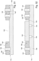
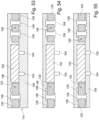
- Figure 51 to Figure 57 illustrate cross-sectional views of structures obtained during carrying out a method of manufacturing a component carrier 100, shown in Figure 57 , according to another exemplary embodiment of the invention. What concerns the embodiment shown in Figure 51 to Figure 57 , reference is made to the similar embodiment described above referring to Figure 40 to Figure 46 .
- the component 102 with the pillars 104 is placed in the cavity 128 face down rather than face up, i.e. with the pillars 104 extending into the temporary carrier 114.
- the thickness of the core 120 may be smaller than or equal to the thickness of the component 102.
- the temporary carrier 114 may be removed from a bottom main surface of the obtained structure, see Figure 54 .
- a carrier body is composed of core 120 and electrically conductive layer structure 108 which delimit the cavity 128.
- the electrically conductive layer structure 108 forms part of the surface of the carrier body 108, 120 (being already covered with a respective electrically insulating layer structure 106 on both opposing main surfaces thereof).
- the component 102 with the pillars 104 it is arranged in the cavity 128, as illustrated in Figure 52 .
- the lower electrically insulating layer structure 106 in Figure 53 accommodates the pillars 104.
- the pillars 104 extend, in a downward direction, vertically beyond the electrically conductive layer structures 108 of the carrier body 108, 120.
- contacting the component 102 via the excessively protruding pillars 104 is significantly simplified (see also the readily manufactured component carrier 100 shown in Figure 57 ).
- an electrically insulating layer structure 106 may then be provided at a bottom side and interconnected with the structure shown in Figure 54 to at least partially cover the pillars 104.
- laser holes 141 may be drilled on both opposing main surfaces of the structure shown in Figure 56 to thereby expose previously embedded electrically conductive layer structures 108.
- these laser holes 141 may be filled with electrically conductive material, for instance by plating.
- electrically conductive layer structures 108 may be formed as electrically conductive contact structures 130 on both opposing main surfaces of the component carrier 100 shown in Figure 57 , for instance patterned copper foils.
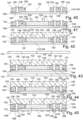
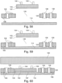
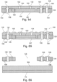
- Figure 58 to Figure 65 illustrate cross-sectional views of structures obtained during carrying out a method of manufacturing a component carrier 100, shown in Figure 65 , according to another exemplary embodiment of the invention.
- a component 102 comprising pillars 104 on one main surface and comprising a pad 197 on the opposing other main surface is provided.
- a core 120 having a through hole type central recess as cavity 128 is provided as well with pillars 104 in a face up configuration.
- a temporary carrier 114 for instance a sticky tape, is provided as well.
- the core 120 is attached to an adhesive surface of the temporary carrier 114.
- the component 102 is inserted into the cavity 128 and is attached to a sticky upper surface of the temporary carrier 114 so that there is a direct physical contact between the pad 197 and the temporary carrier 114.
- An at least partially uncured electrically insulating layer structure 106 for instance a resin sheet or a prepreg sheet, is placed above the mentioned constituents in preparation of the subsequent procedures.
- the at least partially uncured electrically insulating layer structure 106 is laminated onto the core 120 and the component 102 including the pillars 104 so as to form an integral structure. During lamination by applying heat and pressure, the uncured material of layer structure 106 is cured and hardened.
- the temporary carrier 114 is removed from the structure obtained according to Figure 61 , for instance may be peeled off. Since the material of the previously uncured layer structure 106 is now cured and hardened, mechanical support provided by the temporary carrier 114 is no longer necessary.
- the upper main surface of the structure shown in Figure 62 is made subject to a plasma treatment (or any other material removal procedure) to remove a surface portion of the now cured layer structure 106 to expose the free ends 132 of the pillars 104.
- laser via holes are drilled and are at least partially filled with electrically conductive material (for instance are plated with copper) to thereby form electrically conductive contact structure 130.
- electrically conductive layer structures may be attached to both opposing main surfaces of the structure shown in Figure 64 and are patterned to thereby form further constituents of the electrically conductive contact structure 130.
- the illustrated component carrier 100 is appropriate for power applications with power components 102 (such as MOSFETs).
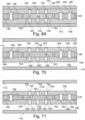
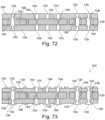
- Figure 66 to Figure 73 illustrate cross-sectional views of structures obtained during carrying out a method of manufacturing a component carrier 100, shown in Figure 73 , according to another exemplary embodiment of the invention.
- a fully cured core 120 with a cavity 128 for accommodating a component 102 is placed above a continuous resin sheet as uncured electrically insulating layer structure 106, which is, in turn, placed above a temporary carrier 114 such as a sticky foil.
- a component 102 having a regular array of pillars 104 extending beyond both opposing main surfaces of the component 102 is arranged above the cavity 128.
- at least a part of the pillars 104 on the opposing main surfaces of the component 102 are connected by electrically conductive connections 193 extending through the component 102, so as to be electrically coupled with one another.
- the component 102 is placed in the cavity 128 so that the pillars 104 on the lower main surface of the component 102 extend into the electrically insulating layer structure 106. In contrast to this, the pillars 104 on the upper main surface of the component 102 protrude upwardly.
- a further electrically insulating layer structure 106 on a further temporary carrier 114 may be arranged above the structure described before.
- the further electrically insulating layer structure 106 on the further temporary carrier 114 are lowered so that the exposed pillars 104 on the upper main surface of the component 102 protrude into the further electrically insulating layer structure 106.
- the obtained constituents may be interconnected by lamination.
- both main surfaces of the structure shown in Figure 70 are made subject to a plasma treatment (or any other material removal procedure) to remove a surface portion of the now cured respective layer structures 106 to expose the free ends 132 of the pillars 104.
- laser via holes are drilled and are at least partially filled with electrically conductive material (for instance a plated with copper) to thereby form electrically conductive contact structure 130.
- electrically conductive layer structures may be attached to both opposing main surfaces of the structure shown in Figure 72 and are patterned to thereby form further constituents of the electrically conductive contact structure 130.
- the illustrated component carrier 100 provides a high density interconnection and a double-sided interconnection.
Landscapes
- Engineering & Computer Science (AREA)
- Microelectronics & Electronic Packaging (AREA)
- Manufacturing & Machinery (AREA)
- Printing Elements For Providing Electric Connections Between Printed Circuits (AREA)
- Connecting Device With Holders (AREA)
- Coupling Device And Connection With Printed Circuit (AREA)
- Production Of Multi-Layered Print Wiring Board (AREA)
- Apparatuses And Processes For Manufacturing Resistors (AREA)
Priority Applications (1)
| Application Number | Priority Date | Filing Date | Title |
|---|---|---|---|
| EP25158168.2A EP4531102A3 (de) | 2017-10-25 | 2017-10-25 | Einbettung einer komponente mit vorverbundener säule in komponententräger |
Applications Claiming Priority (2)
| Application Number | Priority Date | Filing Date | Title |
|---|---|---|---|
| EP25158168.2A EP4531102A3 (de) | 2017-10-25 | 2017-10-25 | Einbettung einer komponente mit vorverbundener säule in komponententräger |
| EP17198423.0A EP3478033B1 (de) | 2017-10-25 | 2017-10-25 | Einbettung von bauteil mit vorverbundener säule in bauteilträger |
Related Parent Applications (1)
| Application Number | Title | Priority Date | Filing Date |
|---|---|---|---|
| EP17198423.0A Division EP3478033B1 (de) | 2017-10-25 | 2017-10-25 | Einbettung von bauteil mit vorverbundener säule in bauteilträger |
Publications (2)
| Publication Number | Publication Date |
|---|---|
| EP4531102A2 true EP4531102A2 (de) | 2025-04-02 |
| EP4531102A3 EP4531102A3 (de) | 2025-07-02 |
Family
ID=60190635
Family Applications (2)
| Application Number | Title | Priority Date | Filing Date |
|---|---|---|---|
| EP17198423.0A Active EP3478033B1 (de) | 2017-10-25 | 2017-10-25 | Einbettung von bauteil mit vorverbundener säule in bauteilträger |
| EP25158168.2A Pending EP4531102A3 (de) | 2017-10-25 | 2017-10-25 | Einbettung einer komponente mit vorverbundener säule in komponententräger |
Family Applications Before (1)
| Application Number | Title | Priority Date | Filing Date |
|---|---|---|---|
| EP17198423.0A Active EP3478033B1 (de) | 2017-10-25 | 2017-10-25 | Einbettung von bauteil mit vorverbundener säule in bauteilträger |
Country Status (3)
| Country | Link |
|---|---|
| US (1) | US10765005B2 (de) |
| EP (2) | EP3478033B1 (de) |
| CN (2) | CN116193764A (de) |
Cited By (1)
| Publication number | Priority date | Publication date | Assignee | Title |
|---|---|---|---|---|
| DE19547117B4 (de) | 1995-08-01 | 2005-10-13 | Deutsche Telekom Ag | Verfahren zur Synchronisation des Decoders bei der Übertragung von quellcodierten Audiosignalen |
Families Citing this family (16)
| Publication number | Priority date | Publication date | Assignee | Title |
|---|---|---|---|---|
| US20200027728A1 (en) * | 2018-07-23 | 2020-01-23 | Intel Corporation | Substrate package with glass dielectric |
| US11557489B2 (en) * | 2018-08-27 | 2023-01-17 | Intel Corporation | Cavity structures in integrated circuit package supports |
| EP3739618A1 (de) | 2019-05-15 | 2020-11-18 | AT & S Austria Technologie & Systemtechnik Aktiengesellschaft | Komponententräger mit in schichtstapel eingebetteter oberflächenkontaktierbarer komponente |
| CN112201652A (zh) | 2019-07-07 | 2021-01-08 | 深南电路股份有限公司 | 线路板及其制作方法 |
| CN111564414B (zh) | 2019-12-12 | 2021-09-24 | 奥特斯(中国)有限公司 | 部件承载件及制造部件承载件的方法 |
| CN111554639A (zh) | 2020-04-02 | 2020-08-18 | 珠海越亚半导体股份有限公司 | 嵌入式芯片封装及其制造方法 |
| CN111863737B (zh) * | 2020-06-15 | 2021-07-20 | 珠海越亚半导体股份有限公司 | 一种嵌入式器件封装基板及其制造方法 |
| CN114141721A (zh) * | 2020-09-04 | 2022-03-04 | 奥特斯奥地利科技与系统技术有限公司 | 具有低溶剂无纤维介电层的部件承载件 |
| EP3975225A1 (de) * | 2020-09-24 | 2022-03-30 | Infineon Technologies Austria AG | Halbleitermodul |
| US11984392B2 (en) * | 2020-09-28 | 2024-05-14 | Infineon Technologies Ag | Semiconductor package having a chip carrier with a pad offset feature |
| CN112770542B (zh) * | 2020-12-10 | 2021-10-29 | 珠海越亚半导体股份有限公司 | 实现立体封装的基板制作方法 |
| US12322622B2 (en) | 2021-03-24 | 2025-06-03 | At&S Austria Technologie & Systemtechnik Aktiengesellschaft | Component carrier with gap around component core and filled with first material in bottom portion and with second material in top portion |
| EP4181179A1 (de) * | 2021-11-16 | 2023-05-17 | Imec VZW | Verfahren zur herstellung eines hybriden halbleiterwafers |
| WO2023158744A1 (en) * | 2022-02-17 | 2023-08-24 | Meta Platforms Technologies, Llc | Battery monitoring units for monitoring battery packs |
| US12616026B2 (en) | 2022-11-30 | 2026-04-28 | Intel Corporation | Permanent layer for bump chip attach |
| CN117118384B (zh) * | 2023-10-23 | 2024-03-22 | 北京超材信息科技有限公司 | 声波元件、声波滤波器及射频模组 |
Citations (2)
| Publication number | Priority date | Publication date | Assignee | Title |
|---|---|---|---|---|
| TW200715930A (en) | 2005-10-14 | 2007-04-16 | Advanced Semiconductor Eng | Method for manufacturing a substrate embedded with an electronic component and device from the same |
| US20140201992A1 (en) | 2013-01-23 | 2014-07-24 | Unimicron Technology Corporation | Circuit board structure having embedded electronic element and fabrication method thereof |
Family Cites Families (18)
| Publication number | Priority date | Publication date | Assignee | Title |
|---|---|---|---|---|
| FR2650471B1 (fr) * | 1989-07-27 | 1991-10-11 | Bull Sa | Procede de formation de piliers du reseau multicouche d'une carte de connexion d'au moins un circuit integre de haute densite |
| EP0805614B1 (de) * | 1995-11-17 | 2005-04-13 | Kabushiki Kaisha Toshiba | Mehrschichtige leiterplatte, vorgefertigtes material für diese leiterplatte, verfahren zur herstellung einer mehrschichtigen leiterplatte, packung elektronischer bauelemente und verfahren zur herstellung vertikaler, elektrisch leitender verbindungen |
| WO2007069789A1 (ja) * | 2005-12-16 | 2007-06-21 | Ibiden Co., Ltd. | 多層プリント配線板およびその製造方法 |
| CN102098876B (zh) * | 2006-04-27 | 2014-04-09 | 日本电气株式会社 | 用于电路基板的制造工艺 |
| KR100836651B1 (ko) * | 2007-01-16 | 2008-06-10 | 삼성전기주식회사 | 소자내장기판 및 그 제조방법 |
| US7936567B2 (en) * | 2007-05-07 | 2011-05-03 | Ngk Spark Plug Co., Ltd. | Wiring board with built-in component and method for manufacturing the same |
| JP2011501410A (ja) * | 2007-10-10 | 2011-01-06 | テッセラ,インコーポレイテッド | 頑健な多層配線要素および埋設された超小型電子素子とのアセンブリ |
| US8383457B2 (en) * | 2010-09-03 | 2013-02-26 | Stats Chippac, Ltd. | Semiconductor device and method of forming interposer frame over semiconductor die to provide vertical interconnect |
| TWI392425B (zh) * | 2009-08-25 | 2013-04-01 | 欣興電子股份有限公司 | 內埋式線路板及其製造方法 |
| US20110290540A1 (en) * | 2010-05-25 | 2011-12-01 | Samsung Electro-Mechanics Co., Ltd. | Embedded printed circuit board and method of manufacturing the same |
| US9824923B2 (en) * | 2011-10-17 | 2017-11-21 | STATS ChipPAC Pte. Ltd. | Semiconductor device and method of forming conductive pillar having an expanded base |
| US9439292B1 (en) * | 2015-03-06 | 2016-09-06 | Kinsus Interconnect Technology Corp. | Method for manufacturing a circuit board with buried element having high density pin count and the circuit board structure |
| FR3036226A1 (fr) * | 2015-05-13 | 2016-11-18 | Commissariat Energie Atomique | Connexion par confinement d'un materiau entre deux elements de contact |
| US11056373B2 (en) * | 2015-07-21 | 2021-07-06 | Apple Inc. | 3D fanout stacking |
| US9875988B2 (en) * | 2015-10-29 | 2018-01-23 | Semtech Corporation | Semiconductor device and method of forming DCALGA package using semiconductor die with micro pillars |
| TWI595612B (zh) * | 2016-03-04 | 2017-08-11 | 力成科技股份有限公司 | 具矽穿孔連續型態之晶圓級晶片尺寸封裝構造及其製造方法 |
| US9859222B1 (en) * | 2016-06-08 | 2018-01-02 | Samsung Electro-Mechanics Co., Ltd. | Fan-out semiconductor package |
| KR102442214B1 (ko) * | 2017-10-12 | 2022-09-13 | 에스케이하이닉스 주식회사 | 반도체 장치 및 그 제조방법 |
-
2017
- 2017-10-25 EP EP17198423.0A patent/EP3478033B1/de active Active
- 2017-10-25 EP EP25158168.2A patent/EP4531102A3/de active Pending
-
2018
- 2018-10-24 US US16/169,741 patent/US10765005B2/en active Active
- 2018-10-25 CN CN202310317723.3A patent/CN116193764A/zh active Pending
- 2018-10-25 CN CN201811253212.5A patent/CN109712894B/zh active Active
Patent Citations (2)
| Publication number | Priority date | Publication date | Assignee | Title |
|---|---|---|---|---|
| TW200715930A (en) | 2005-10-14 | 2007-04-16 | Advanced Semiconductor Eng | Method for manufacturing a substrate embedded with an electronic component and device from the same |
| US20140201992A1 (en) | 2013-01-23 | 2014-07-24 | Unimicron Technology Corporation | Circuit board structure having embedded electronic element and fabrication method thereof |
Cited By (1)
| Publication number | Priority date | Publication date | Assignee | Title |
|---|---|---|---|---|
| DE19547117B4 (de) | 1995-08-01 | 2005-10-13 | Deutsche Telekom Ag | Verfahren zur Synchronisation des Decoders bei der Übertragung von quellcodierten Audiosignalen |
Also Published As
| Publication number | Publication date |
|---|---|
| EP3478033B1 (de) | 2025-02-19 |
| EP4531102A3 (de) | 2025-07-02 |
| CN116193764A (zh) | 2023-05-30 |
| CN109712894B (zh) | 2023-04-14 |
| EP3478033A1 (de) | 2019-05-01 |
| US10765005B2 (en) | 2020-09-01 |
| CN109712894A (zh) | 2019-05-03 |
| US20190124772A1 (en) | 2019-04-25 |
Similar Documents
| Publication | Publication Date | Title |
|---|---|---|
| US10765005B2 (en) | Embedding component with pre-connected pillar in component carrier | |
| US11810844B2 (en) | Component carrier and method of manufacturing the same | |
| US12400968B2 (en) | Component with dielectric layer for embedding in component carrier | |
| US10790234B2 (en) | Embedding known-good component in known-good cavity of known-good component carrier material with pre-formed electric connection structure | |
| US10743422B2 (en) | Embedding a component in a core on conductive foil | |
| EP3836209B1 (de) | Komponententräger und dessen herstellung | |
| US11324122B2 (en) | Component carrier and method of manufacturing the same | |
| US10643949B2 (en) | Component carrier and method for manufacturing the same | |
| CN112702840A (zh) | 有嵌入的部件和水平长型过孔的部件承载件及其制造方法 | |
| US12167529B2 (en) | Heat removal architecture for stack-type component carrier with embedded component | |
| US11058004B2 (en) | Metallic layer as carrier for component embedded in cavity of component carrier | |
| EP3349247B1 (de) | Strukturierte deckschicht auf basisstruktur zur definition eines hohlraums und ausrichtungsmarkierung | |
| EP3340753B1 (de) | Verfahren einen verbinder in komponententräger zu integrieren | |
| EP3846598A1 (de) | Anordnung mit einem zentralen träger und zwei gegenüberliegenden schichtstapeln, komponententräger und herstellungsverfahren | |
| US10863631B2 (en) | Layer stack of component carrier material with embedded components and common high temperature robust dielectric structure | |
| US20240021440A1 (en) | Component Carrier and Method of Manufacturing the Same |
Legal Events
| Date | Code | Title | Description |
|---|---|---|---|
| PUAI | Public reference made under article 153(3) epc to a published international application that has entered the european phase |
Free format text: ORIGINAL CODE: 0009012 |
|
| STAA | Information on the status of an ep patent application or granted ep patent |
Free format text: STATUS: THE APPLICATION HAS BEEN PUBLISHED |
|
| AC | Divisional application: reference to earlier application |
Ref document number: 3478033 Country of ref document: EP Kind code of ref document: P |
|
| AK | Designated contracting states |
Kind code of ref document: A2 Designated state(s): AL AT BE BG CH CY CZ DE DK EE ES FI FR GB GR HR HU IE IS IT LI LT LU LV MC MK MT NL NO PL PT RO RS SE SI SK SM TR |
|
| REG | Reference to a national code |
Ref country code: DE Ref legal event code: R079 Free format text: PREVIOUS MAIN CLASS: H01L0023538000 Ipc: H05K0001180000 |
|
| PUAL | Search report despatched |
Free format text: ORIGINAL CODE: 0009013 |
|
| AK | Designated contracting states |
Kind code of ref document: A3 Designated state(s): AL AT BE BG CH CY CZ DE DK EE ES FI FR GB GR HR HU IE IS IT LI LT LU LV MC MK MT NL NO PL PT RO RS SE SI SK SM TR |
|
| RIC1 | Information provided on ipc code assigned before grant |
Ipc: H01L 23/538 20060101ALI20250526BHEP Ipc: H01L 23/00 20060101ALI20250526BHEP Ipc: H05K 3/00 20060101ALI20250526BHEP Ipc: H05K 1/18 20060101AFI20250526BHEP |
|
| STAA | Information on the status of an ep patent application or granted ep patent |
Free format text: STATUS: REQUEST FOR EXAMINATION WAS MADE |
|
| 17P | Request for examination filed |
Effective date: 20251202 |