EP3340753B1 - Verfahren einen verbinder in komponententräger zu integrieren - Google Patents
Verfahren einen verbinder in komponententräger zu integrieren Download PDFInfo
- Publication number
- EP3340753B1 EP3340753B1 EP16206325.9A EP16206325A EP3340753B1 EP 3340753 B1 EP3340753 B1 EP 3340753B1 EP 16206325 A EP16206325 A EP 16206325A EP 3340753 B1 EP3340753 B1 EP 3340753B1
- Authority
- EP
- European Patent Office
- Prior art keywords
- connector member
- layer structure
- component carrier
- electrically insulating
- flow
- Prior art date
- Legal status (The legal status is an assumption and is not a legal conclusion. Google has not performed a legal analysis and makes no representation as to the accuracy of the status listed.)
- Active
Links
Images

Classifications
-
- H—ELECTRICITY
- H05—ELECTRIC TECHNIQUES NOT OTHERWISE PROVIDED FOR
- H05K—PRINTED CIRCUITS; CASINGS OR CONSTRUCTIONAL DETAILS OF ELECTRIC APPARATUS; MANUFACTURE OF ASSEMBLAGES OF ELECTRICAL COMPONENTS
- H05K1/00—Printed circuits
- H05K1/18—Printed circuits structurally associated with non-printed electric components
- H05K1/182—Printed circuits structurally associated with non-printed electric components associated with components mounted in printed circuit boards [PCB], e.g. insert-mounted components [IMC]
- H05K1/185—Printed circuits structurally associated with non-printed electric components associated with components mounted in printed circuit boards [PCB], e.g. insert-mounted components [IMC] associated with components encapsulated in the insulating substrate of the PCBs; associated with components incorporated in internal layers of multilayer circuit boards
- H05K1/186—Printed circuits structurally associated with non-printed electric components associated with components mounted in printed circuit boards [PCB], e.g. insert-mounted components [IMC] associated with components encapsulated in the insulating substrate of the PCBs; associated with components incorporated in internal layers of multilayer circuit boards manufactured by mounting on or connecting to patterned circuits before or during embedding
-
- H—ELECTRICITY
- H05—ELECTRIC TECHNIQUES NOT OTHERWISE PROVIDED FOR
- H05K—PRINTED CIRCUITS; CASINGS OR CONSTRUCTIONAL DETAILS OF ELECTRIC APPARATUS; MANUFACTURE OF ASSEMBLAGES OF ELECTRICAL COMPONENTS
- H05K3/00—Apparatus or processes for manufacturing printed circuits
- H05K3/46—Manufacturing multilayer circuits
- H05K3/4697—Manufacturing multilayer circuits having cavities, e.g. for mounting components
-
- H—ELECTRICITY
- H01—ELECTRIC ELEMENTS
- H01R—ELECTRICALLY-CONDUCTIVE CONNECTIONS; STRUCTURAL ASSOCIATIONS OF A PLURALITY OF MUTUALLY-INSULATED ELECTRICAL CONNECTING ELEMENTS; COUPLING DEVICES; CURRENT COLLECTORS
- H01R12/00—Structural associations of a plurality of mutually-insulated electrical connecting elements, specially adapted for printed circuits, e.g. printed circuit boards [PCB], flat or ribbon cables, or like generally planar structures, e.g. terminal strips, terminal blocks; Coupling devices specially adapted for printed circuits, flat or ribbon cables, or like generally planar structures; Terminals specially adapted for contact with, or insertion into, printed circuits, flat or ribbon cables, or like generally planar structures
- H01R12/70—Coupling devices
- H01R12/71—Coupling devices for rigid printing circuits or like structures
- H01R12/72—Coupling devices for rigid printing circuits or like structures coupling with the edge of the rigid printed circuits or like structures
- H01R12/73—Coupling devices for rigid printing circuits or like structures coupling with the edge of the rigid printed circuits or like structures connecting to other rigid printed circuits or like structures
-
- H—ELECTRICITY
- H05—ELECTRIC TECHNIQUES NOT OTHERWISE PROVIDED FOR
- H05K—PRINTED CIRCUITS; CASINGS OR CONSTRUCTIONAL DETAILS OF ELECTRIC APPARATUS; MANUFACTURE OF ASSEMBLAGES OF ELECTRICAL COMPONENTS
- H05K2201/00—Indexing scheme relating to printed circuits covered by H05K1/00
- H05K2201/09—Shape and layout
- H05K2201/09009—Substrate related
- H05K2201/09127—PCB or component having an integral separable or breakable part
-
- H—ELECTRICITY
- H05—ELECTRIC TECHNIQUES NOT OTHERWISE PROVIDED FOR
- H05K—PRINTED CIRCUITS; CASINGS OR CONSTRUCTIONAL DETAILS OF ELECTRIC APPARATUS; MANUFACTURE OF ASSEMBLAGES OF ELECTRICAL COMPONENTS
- H05K2201/00—Indexing scheme relating to printed circuits covered by H05K1/00
- H05K2201/09—Shape and layout
- H05K2201/09209—Shape and layout details of conductors
- H05K2201/09654—Shape and layout details of conductors covering at least two types of conductors provided for in H05K2201/09218 - H05K2201/095
- H05K2201/09754—Connector integrally incorporated in the printed circuit board [PCB] or in housing
-
- H—ELECTRICITY
- H05—ELECTRIC TECHNIQUES NOT OTHERWISE PROVIDED FOR
- H05K—PRINTED CIRCUITS; CASINGS OR CONSTRUCTIONAL DETAILS OF ELECTRIC APPARATUS; MANUFACTURE OF ASSEMBLAGES OF ELECTRICAL COMPONENTS
- H05K2201/00—Indexing scheme relating to printed circuits covered by H05K1/00
- H05K2201/10—Details of components or other objects attached to or integrated in a printed circuit board
- H05K2201/10007—Types of components
- H05K2201/10189—Non-printed connector
-
- H—ELECTRICITY
- H05—ELECTRIC TECHNIQUES NOT OTHERWISE PROVIDED FOR
- H05K—PRINTED CIRCUITS; CASINGS OR CONSTRUCTIONAL DETAILS OF ELECTRIC APPARATUS; MANUFACTURE OF ASSEMBLAGES OF ELECTRICAL COMPONENTS
- H05K2203/00—Indexing scheme relating to apparatus or processes for manufacturing printed circuits covered by H05K3/00
- H05K2203/02—Details related to mechanical or acoustic processing, e.g. drilling, punching, cutting, using ultrasound
- H05K2203/0207—Partly drilling through substrate until a controlled depth, e.g. with end-point detection
-
- H—ELECTRICITY
- H05—ELECTRIC TECHNIQUES NOT OTHERWISE PROVIDED FOR
- H05K—PRINTED CIRCUITS; CASINGS OR CONSTRUCTIONAL DETAILS OF ELECTRIC APPARATUS; MANUFACTURE OF ASSEMBLAGES OF ELECTRICAL COMPONENTS
- H05K2203/00—Indexing scheme relating to apparatus or processes for manufacturing printed circuits covered by H05K3/00
- H05K2203/02—Details related to mechanical or acoustic processing, e.g. drilling, punching, cutting, using ultrasound
- H05K2203/0228—Cutting, sawing, milling or shearing
-
- H—ELECTRICITY
- H05—ELECTRIC TECHNIQUES NOT OTHERWISE PROVIDED FOR
- H05K—PRINTED CIRCUITS; CASINGS OR CONSTRUCTIONAL DETAILS OF ELECTRIC APPARATUS; MANUFACTURE OF ASSEMBLAGES OF ELECTRICAL COMPONENTS
- H05K2203/00—Indexing scheme relating to apparatus or processes for manufacturing printed circuits covered by H05K3/00
- H05K2203/03—Metal processing
- H05K2203/0361—Stripping a part of an upper metal layer to expose a lower metal layer, e.g. by etching or using a laser
-
- H—ELECTRICITY
- H05—ELECTRIC TECHNIQUES NOT OTHERWISE PROVIDED FOR
- H05K—PRINTED CIRCUITS; CASINGS OR CONSTRUCTIONAL DETAILS OF ELECTRIC APPARATUS; MANUFACTURE OF ASSEMBLAGES OF ELECTRICAL COMPONENTS
- H05K2203/00—Indexing scheme relating to apparatus or processes for manufacturing printed circuits covered by H05K3/00
- H05K2203/06—Lamination
- H05K2203/063—Lamination of preperforated insulating layer
-
- H—ELECTRICITY
- H05—ELECTRIC TECHNIQUES NOT OTHERWISE PROVIDED FOR
- H05K—PRINTED CIRCUITS; CASINGS OR CONSTRUCTIONAL DETAILS OF ELECTRIC APPARATUS; MANUFACTURE OF ASSEMBLAGES OF ELECTRICAL COMPONENTS
- H05K3/00—Apparatus or processes for manufacturing printed circuits
- H05K3/46—Manufacturing multilayer circuits
- H05K3/4611—Manufacturing multilayer circuits by laminating two or more circuit boards
- H05K3/4614—Manufacturing multilayer circuits by laminating two or more circuit boards the electrical connections between the circuit boards being made during lamination
- H05K3/4617—Manufacturing multilayer circuits by laminating two or more circuit boards the electrical connections between the circuit boards being made during lamination characterized by laminating only or mainly similar single-sided circuit boards
Definitions
- the invention relates to a method of manufacturing a component carrier.
- Connector members may be integrated with printed circuit boards (PCB).
- PCB printed circuit boards
- a corresponding manufacture is challenging.
- PCBs with connector member may suffer from reliability issues.
- WO 2014/131071 A2 discloses a semi-finished product for the production of a printed circuit board with alternating electrically conductive and electrically insulating layers.
- An electronic component is mounted via an anisotropic film onto one of the electrically layers. Then, the electronic component is embedded in an electrically insulating layer of prepreg and the semi-finished product is further processed.
- the insulating layer, which embeds the component, comprises hereby a clearance into which the electronic component may be arranged.
- US 2012/0160803 A1 discloses a method for manufacturing a multilayer printed circuit board. Hereby, no liquid should remain in the cavity which is for accommodating the electronic component.
- the circuit board comprises alternating electrically conductive and electrically insulating layers, wherein the cavity is located below one of the electrically insulating layers.
- WO 2012/053728 A1 discloses a printed circuit board comprising a cavity for placing an electronic component.
- the circuit board comprises alternating electrically conductive and electrically insulating layers.
- it is proposed to perform two laser drillings down to the embedded circuit pattern. Due to the very low adhesion strength of a cavity separation layer, the layers above the circuit pattern can be removed in a feasible manner. Finally, the circuit pattern in the cavity is exposed and can be connected to an active or passive device.
- US 2015/194753 A1 discloses mid-plane board-to-board connectors for connection two circuit boards, wherein the connectors require reduced space (low height).
- the lower connector is at least partially arranged in a recess of the respective circuit board.
- a component carrier In order to achieve the object defined above, a component carrier, a semifinished product, a connector arrangement and methods of manufacturing a component carrier according to the independent claims are provided.
- a method of manufacturing a component carrier comprising
- a method of manufacturing a component carrier comprises at least partially surrounding a connector member by a plurality of electrically insulating layer structures comprising a polymer (in particular a resin or another dielectric material), and, during the surrounding, inhibiting a flow of polymer into an interior of the connector member.
- a polymer in particular a resin or another dielectric material
- a semifinished product obtainable during manufacturing a component carrier comprising a connector member, and a plurality of layer structures surrounding the connector member so that the connector member is accommodated in a void volume within the layer structures.
- a component carrier which comprises a plurality of layer structures, at least one of which comprising low-flow resin or no-flow resin, and a connector member on and/or surrounded by the layer structure, wherein an interior of the connector member is free of the low-flow resin or no-flow resin.
- a component carrier which comprises a plurality of laminated layer structures defining a recess (which may be delimited along at least part of its circumference by a side wall, but which may for instance also be open at a lateral side), in particular a cavity (which may be delimited along its entire circumference by a side wall), and a connector member at least partially in the recess and on and/or at least partially surrounded by the layer structures.
- layer structure may particularly denote one or more full or continuous layers, one or more patterned layers, and/or a plurality of islands-type separate elements formed together within a plane.
- component carrier may particularly denote any support structure which is capable of accommodating one or more components thereon and/or therein for providing mechanical support and/or electrical connectivity.
- a component carrier may be configured as a mechanical and/or electronic carrier for components.
- a component carrier may be one of a printed circuit board, an organic interposer, and an IC (integrated circuit) substrate.
- a component carrier may also be a hybrid board combining different ones of the above mentioned types of component carriers.
- low-flow material may particularly denote material which has no or only a very limited tendency to flow during processing under external pressure and elevated temperature, in particular during lamination.
- low-flow material may have a sufficiently high viscosity, for instance at least 5000 Poise, preferably at least 10000 Poise, at lamination temperature (for instance 150°C).
- lamination temperature for instance 150°C.
- ordinary prepreg when heated under pressure, its resin melts (liquefies) and freely flows in any voids in the environment. There is a certain period of time during which the resin of ordinary prepreg remains fluidic enough to flow freely.
- low-flow material as implemented in accordance with exemplary embodiments of the invention is specifically configured to suppress or even eliminate flow during lamination, so that the low-flow material substantially rests in place during lamination.
- the "low-flow material” or “no-flow material” may still be at least partially uncured when being provided prior to lamination.
- a semifinished product may particularly denote a physical structure which is not yet readily manufactured but requires further processing to obtain a final product which can functionally serve as stand-alone component carrier.
- a semifinished product may be a pre-form of a component carrier to be manufactured based on the semifinished product.
- a connector member is integrated with electrically insulating and/or electrically conductive layer structures of a component carrier by firstly mounting the connector member on such a layer structure, by subsequently laminating a further layer structure onto the previously mentioned layer structure including surface mounted connector member, and by thereafter exposing the connector member with regard to an environment of the component carrier by removing a portion of the material of one or both of the layer structures.
- it is dispensable to mount the connector member in a preformed cavity of a layer structure by soldering, which is conventionally a difficult task.
- an exemplary embodiment of the invention does not put any limitation on the topology of a surface of the layer structure on which the connector member is to be mounted.
- a cavity for accommodating the connector member can be formed advantageously during or after having mounted the connector member on a layer structure, i.e. by an additive process. By locating or sinking at least part of the connector member in such a cavity formed after mounting the connector member, a highly stable, properly protected and compact component carrier with integrated connector function may be manufactured.
- At least one of the layer structures comprises at least one of the group consisting of at least one electrically insulating layer structure and/or at least one electrically conductive layer structure.
- the connector member may be mounted on or within a dielectric and/or a metallic material of a stack below and/or above the connector member.
- the interconnecting comprises laminating the further layer structure with the connector member and the layer structure.
- Lamination may be accomplished by the application of mechanical pressure, if desired or required in combination with heat.
- the connector member is mounted on or electrically coupled to the layer structure by at least one of the group consisting of forming a copper connection, soldering and gluing, in particular using at least one of an Anisotropic Conductive Film (ACF), and an Anisotropic Conductive Paste (ACP).
- ACF is an adhesive interconnect system in the shape of a film that may be used to establish electrical and mechanical connections.
- ACF can be used alternatively in a paste form referred to as ACP.
- the connector member By taking this measure, it is possible to design a reliable electric interconnection between the connector member and the layer structure (which may be an electrically insulating structure which may have one or more electrically conductive elements embedded therein, also denoted as electrically conductive layer structure) without the need to involve high temperature processes.
- the layer structure which may be an electrically insulating structure which may have one or more electrically conductive elements embedded therein, also denoted as electrically conductive layer structure
- exposing the connector member comprises forming a cavity in at least one of the layer structures.
- cavity formation may hence be carried out after having mounted to the connector member so that a cumbersome mounting process of the connector member in a preformed cavity can be omitted.
- Mounting of the connector member in a preformed cavity is conventionally particularly critical when the connection to be made is a solder connection.
- the connector member After the interconnecting and the exposing, at least a portion of the connector member remains sunk within at least one of the layer structure and of the further layer structure.
- the connector member may be retracted within the cavity with regard to an exterior surface of the component carrier so that the connector member can be mechanically protected with regard to a mechanical impact from the environment. Moreover, this results in a compact design of the component carrier.
- the term "sinking" of the connector member shall cover both a hidden or retracted location of the connector member in the cavity (as for example in Figure 4 ), but also an at least partial embedding of the connector member (also of lateral surfaces thereof) within one or more of the layer structures (as for example in Figure 5 ).
- the connector member is mounted on a substantially planar layer (rather than within a cavity) of the layer structure. This simplifies the mounting procedure.
- the further layer structure which is provided with a recess, is attached on the layer structure with the connector member being at least partially located within the recess. Recessing the further layer structure may allow to keep (in particular dielectric) material of the further layer structure sufficiently far away from the connector member so that, during lamination, there is no risk that material of the further layer structure flows into tiny connection structures of the connector member.
- the further layer structure is attached to (fully or partially) cover the connector member (for instance to hermetically encapsulate the connector member).
- the top of the connector member may be temporarily covered (with or without contact) by (in particular electrically insulating) material prior to the removal, and as a result of the lamination.
- the removing comprises laser cutting.
- This allows to precisely define a cap portion which can be removed from the rest of the component carrier to be manufactured.
- material removal by a mechanical procedure is possible, for instance by mechanically drilling, routing etc. This allows to precisely define size and position of the cavity in which the connector member is mounted.
- a combination of an additive process (i.e. the lamination of the further layer structure) with a subtractive process (i.e. the material removal) may be carried out.
- the flow of polymer (in particular resin) into the connector member is inhibited by configuring at least a part of the plurality of (in particular electrically insulating) layer structures from low-flow prepreg or no-flow prepreg.
- the polymer or resin of such prepreg material has only a very limited or even no tendency of flowing into a surrounding during lamination. This material selection protects the connector member against contamination.
- the connector member is mounted on a core, in particular on a fully cured core.
- core may particularly denote already cured electrically insulating material providing a stable base for one or more electronic components.
- a core may be made of cured resin (such as epoxy resin) with fibers (such as glass fibers) embedded therein, for example FR4.
- fibers such as glass fibers
- a core may be made of a thickness being higher than that of a single layer (such as a prepreg layer) as used in PCB technology.
- the term "fully cured” may particularly denote a material property according to which the corresponding material (such as resin) is not capable any more of being re-melted to become flowable and of being subsequently re-solidified for interconnecting various elements of the manufactured component carrier.
- resin material of the fully cured core may be already cross-linked.
- the fully cured core material may be C-stage material rather than A-stage or B-stage material.
- a flow of polymer or resin into a functional connector structure of the connector member is prevented.
- This can be accomplished by one or more of the following measures: using precut electrically insulating or electrically conductive layers in particular of the further layer structure for spacing the mounted connector member with regard to surrounding dielectric material; using no-flow prepreg or low-flow prepreg for any of the layer structures for suppressing resin flow during lamination (in particular for a layer structure located next to the connector member); using fully cured dielectric material (in particular a core) for any of the layer structures for disabling resin flow during lamination.
- the connector member is a female connector member (i.e. having an indentation to be filled by a protrusion of a male connector member) configured for cooperating with a male connector member (i.e. having the protrusion for filling the indentation of the female connector member).
- the connector member may be also a male connector member configured for cooperating with a female connector member.
- the connector member is configured for establishing an electric connection with a counter connector member.
- the connection function may not only establish a mechanical connection (by a form closure, by friction connection, or the like), but may also simultaneously establish an electric connection (in particular by the coupling of one or more electric contacts of the connector member with one or more electric contacts of the counter connector member).
- one or more electric contacts of the connector member may be electrically coupled with the electrically conductive layer structure of the component carrier.
- the one or more electric contacts of the counter connector member may be also electrically coupled with an electrically conductive layer structure of the electronic device.
- the component carrier comprises at least one electronic component embedded in at least one of the layer structure and the further layer structure.
- the layer structures may be synergistically used also for embedding a component which increases the level of functionality of the component carrier.
- the component is electrically coupled with the connector member. This can be accomplished with low effort by the electrically conductive layer structure of the component carrier.
- the at least one component can be selected from a group consisting of an electrically non-conductive inlay, an electrically conductive inlay (such as a metal inlay, preferably comprising copper or aluminum), a heat transfer unit (for example a heat pipe), a light guiding element (for example an optical waveguide or a light conductor connection), an electronic component, or combinations thereof.
- an electrically non-conductive inlay such as a metal inlay, preferably comprising copper or aluminum
- a heat transfer unit for example a heat pipe
- a light guiding element for example an optical waveguide or a light conductor connection
- an electronic component or combinations thereof.
- a magnetic element can be used as a component.
- a magnetic element may be a permanent magnetic element (such as a ferromagnetic element, an antiferromagnetic element or a ferrimagnetic element, for instance a ferrite core) or may be a paramagnetic element.
- the component may also be a further component carrier, for example in a board-in-board configuration.
- the component may be surface mounted on the component carrier and/or may be embedded in an interior thereof.
- other components in particular those which generate and emit electromagnetic radiation and/or are sensitive with regard to electromagnetic radiation propagating from an environment, may be used as component.
- the component carrier comprises a stack of at least one electrically insulating layer structure and at least one electrically conductive layer structure.
- the component carrier may be a laminate of the mentioned electrically insulating layer structure(s) and electrically conductive layer structure(s), in particular formed by applying mechanical pressure, if desired supported by thermal energy.
- the mentioned stack may provide a plate-shaped component carrier capable of providing a large mounting surface for further components and being nevertheless very thin and compact.
- layer structure may particularly denote a continuous layer, a patterned layer or a plurality of non-consecutive islands within a common plane.
- the component carrier is shaped as a plate. This contributes to the compact design, wherein the component carrier nevertheless provides a large basis for mounting components thereon. Furthermore, in particular a naked die as example for an embedded electronic component, can be conveniently embedded, thanks to its small thickness, into a thin plate such as a printed circuit board.
- the component carrier is configured as one of the group consisting of a printed circuit board, and a substrate (in particular an IC substrate).
- PCB printed circuit board
- a component carrier which may be plate-shaped (i.e. planar), three-dimensionally curved (for instance when manufactured using 3D printing) or which may have any other shape) which is formed by laminating several electrically conductive layer structures with several electrically insulating layer structures, for instance by applying pressure, if desired accompanied by the supply of thermal energy.
- the electrically conductive layer structures are made of copper
- the electrically insulating layer structures may comprise resin and/or glass fibers, so-called prepreg or FR4 material.
- the various electrically conductive layer structures may be connected to one another in a desired way by forming through-holes through the laminate, for instance by laser drilling or mechanical drilling, and by filling them with electrically conductive material (in particular copper), thereby forming vias as through-hole connections.
- electrically conductive material in particular copper
- a printed circuit board is usually configured for accommodating one or more components on one or both opposing surfaces of the plate-shaped printed circuit board. They may be connected to the respective main surface by soldering.
- a dielectric part of a PCB may be composed of resin with reinforcing fibers (such as glass fibers).
- the term "substrate” may particularly denote a small component carrier having substantially the same size as a component (in particular an electronic component) to be mounted thereon. More specifically, a substrate can be understood as a carrier for electrical connections or electrical networks as well as component carrier comparable to a printed circuit board (PCB), however with a considerably higher density of laterally and/or vertically arranged connections. Lateral connections are for example conductive paths, whereas vertical connections may be for example drill holes. These lateral and/or vertical connections are arranged within the substrate and can be used to provide electrical and/or mechanical connections of housed components or unhoused components (such as bare dies), particularly of IC chips, with a printed circuit board or intermediate printed circuit board. Thus, the term “substrate” also includes "IC substrates". A dielectric part of a substrate may be composed of resin with reinforcing spheres (such as glass spheres).
- the at least one electrically insulating layer structure comprises at least one of the group consisting of resin (such as reinforced or non-reinforced resins, for instance epoxy resin or Bismaleimide-Triazine resin, more specifically FR-4 or FR-5), cyanate ester, polyphenylene derivate, glass (in particular glass fibers, multi-layer glass, glass-like materials), prepreg material, polyimide, polyamide, liquid crystal polymer (LCP), epoxy-based Build-Up Film, polytetrafluoroethylene (Teflon), a ceramic, and a metal oxide. Reinforcing materials such as webs, fibers or spheres, for example made of glass (multilayer glass) may be used as well.
- resin such as reinforced or non-reinforced resins, for instance epoxy resin or Bismaleimide-Triazine resin, more specifically FR-4 or FR-5
- cyanate ester polyphenylene derivate
- glass in particular glass fibers, multi-layer glass, glass-like materials
- prepreg or FR4 are usually preferred, other materials may be used as well.
- high-frequency materials such as polytetrafluoroethylene, liquid crystal polymer and/or cyanate ester resins may be implemented in the component carrier as electrically insulating layer structure.
- the at least one electrically conductive layer structure comprises at least one of the group consisting of copper, aluminum, nickel, silver, gold, palladium, and tungsten.
- copper is usually preferred, other materials or coated versions thereof are possible as well, in particular coated with supra-conductive material such as graphene.
- the component carrier is a laminate-type component carrier.
- the component carrier is a compound of multiple layer structures which are stacked and connected together by applying a pressing force, if desired accompanied by heat.
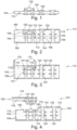
- Figure 1 to Figure 4 illustrate different cross-sectional views of structures obtained during carrying out a method of manufacturing a component carrier according to an exemplary embodiment of the invention.
- Figure 5 illustrates a cross-sectional view of a component carrier according to another exemplary embodiment of the invention.
- an embedded connector member is provided which is integrated in a component carrier.
- resin (in particular prepreg) viscosity and flow control may be implemented to enable to mount or embed a connector member in of a PCB.
- an exemplary embodiment of the invention provides a PCB board, in which a Btb or ZIP or other type of connector member is placed inside of the PCB stack up with an embedding technology (including surface mounting technology (SMT), Anisotropic Conductive Film (ACF) placement, sequential embedding, cavity embedding, etc.).
- a corresponding treatment may be adapted so that the connector may be covered by a cured PCB core, and a low-flow dielectric material may be used to laminate the cover core to the main core.
- Figure 1 to Figure 4 illustrate different cross-sectional views of structures obtained during carrying out a method of manufacturing a component carrier 100, as shown in Figure 4 , according to an exemplary embodiment of the invention.
- a preformed connector member 102 is mounted on an electrically insulating layer structure 104 and on an electrically conductive layer structure 124.
- the connector member 102 may comprise a plastic part formed by molding, wherein an electrically conductive wiring structure may be located in and/or on the plastic part.
- the connector member 102 may be configured for establishing simultaneously a mechanical connection and an electric connection with a counter connector member 120 (see Figure 4 ), upon being plugged together by a user.
- the connector member 102 is mounted on the electrically insulating layer structure 104 in a way to be thereby simultaneously electrically connected to the electrically conductive layer structure 124 of the shown base layer stack composed of electrically insulating layer structure 104 and electrically conductive layer structure 124.
- the electrically conductive mounting of the connector member 102 on the described base layer stack can be accomplished by gluing using an Anisotropic Conductive Film (ACF) or an Anisotropic Conductive Paste (ACP). It is alternatively also possible to solder the connector member 102 onto the electrically conductive layer structure 124.
- ACF Anisotropic Conductive Film
- ACP Anisotropic Conductive Paste
- the electrically conductive layer structure 124 may be formed partially on and partially in the electrically insulating layer structure 104 by connection and patterning of metal foils (such as copper foils), and by the formation of through holes (such as vias which may be formed by laser drilling or mechanically drilling) with a subsequent filling of these through holes with electrically conductive material (for instance with copper, for example by plating).
- the connector member 102 is mounted on a substantially planar surface of the electrically insulating layer structure 104, i.e. on a planar surface rather than within a preformed cavity. Such a mounting procedure on a planar support surface is significantly simpler than soldering the connector member 102 within a preformed cavity, as done conventionally.
- the connector member 102 is mounted on a fully cured core 112 in form of the electrically insulating layer structure 104.
- the fully cured core 112 may comprise reinforcing less fibers in a matrix of epoxy resin, being already in the C-stage rather than in the A-stage or the B-stage.
- the fully cured core 112 may have the property that its intrinsic resin does not remelt upon lamination (compare Figure 2 ), so that the resin of the fully cured core 112 is advantageously incapable of flowing into internal recesses or gaps within the connector member 102 upon lamination.
- the mechanical and electric functionality of the connector member 102 is not negatively influenced by the lamination procedure thanks to the provision of the electrically insulating layer structure 104 of already fully cured material.
- a PCB core 112 is created.
- the connector member 102 (which is here embodied as a female part of a two-part connector, but which may alternatively also be a male part of the connector) may be placed on the core 112.
- the further electrically insulating layer structure 110 is attached to cover the connector member 102 with a gap in between.
- the connector member 102 is surrounded by the described plurality of electrically insulating layer structures 104, 110 which all comprise resin and is temporarily hermetically encapsulated and located within an internal hollow space.
- the further electrically insulating layer structure 110 is composed of a further fully cured core 162 and of a no-flow prepreg layer 160 below the further fully cured core 162.
- the recess 108 is delimited by and between the fully cured core 112, the further fully cured core 162 as well as the no-flow prepreg layer 160.
- the other electrically insulating layer structure 158 is composed of yet another fully cured core 166 and of a further no-flow prepreg layer 164 above the other fully cured core 166.
Landscapes
- Engineering & Computer Science (AREA)
- Manufacturing & Machinery (AREA)
- Microelectronics & Electronic Packaging (AREA)
- Production Of Multi-Layered Print Wiring Board (AREA)
- Laminated Bodies (AREA)
Claims (5)
- Ein Verfahren zum Herstellen eines Komponententrägers (100), wobei das Verfahren aufweist:Montieren eines Konnektorelements (102) auf einer im Wesentlichen planaren Schichtstruktur (104);Verbinden einer weiteren Schichtstruktur (110) mit der Schichtstruktur (104),wobei nach dem Montieren die weitere Schichtstruktur (110), die mit einer Aussparung (108) versehen ist, an der Schichtstruktur (104) angebracht wird, wobei das Konnektorelement (102) zumindest teilweise innerhalb der Aussparung (108) angeordnet ist;
nach dem Verbinden, Freilegen zumindest eines Teils des Konnektorelements (102) durch Entfernen von Material von zumindest einer der Schichtstrukturen (104, 110); wobei nach dem Verbinden und dem Freilegen zumindest ein Abschnitt des Konnektorelements (102) innerhalb der weiteren Schichtstruktur (110) vertieft bleibt. - Das Verfahren gemäß Anspruch 1, wobei zumindest eine der Schichtstrukturen (104, 110) zumindest eines aus der Gruppe aufweist, die aus zumindest einer elektrisch isolierenden Schichtstruktur und/oder zumindest einer elektrisch leitfähigen Schichtstruktur besteht.
- Das Verfahren gemäß Anspruch 1 oder 2, wobei das Verbinden ein Laminieren der weiteren Schichtstruktur (110) mit der Schichtstruktur (104) aufweist.
- Das Verfahren gemäß einem der Ansprüche 1 bis 3, wobei die weitere Schichtstruktur (110) so angebracht wird, dass sie das Konnektorelement (102) mit einer Lücke dazwischen bedeckt.
- Das Verfahren gemäß einem der Ansprüche 1 bis 4, wobei das Entfernen ein Laserschneiden aufweist.
Priority Applications (2)
| Application Number | Priority Date | Filing Date | Title |
|---|---|---|---|
| EP25153279.2A EP4521860A3 (de) | 2016-12-22 | 2016-12-22 | Verfahren zur integration eines verbinderelements mit komponententräger |
| EP16206325.9A EP3340753B1 (de) | 2016-12-22 | 2016-12-22 | Verfahren einen verbinder in komponententräger zu integrieren |
Applications Claiming Priority (1)
| Application Number | Priority Date | Filing Date | Title |
|---|---|---|---|
| EP16206325.9A EP3340753B1 (de) | 2016-12-22 | 2016-12-22 | Verfahren einen verbinder in komponententräger zu integrieren |
Related Child Applications (2)
| Application Number | Title | Priority Date | Filing Date |
|---|---|---|---|
| EP25153279.2A Division EP4521860A3 (de) | 2016-12-22 | 2016-12-22 | Verfahren zur integration eines verbinderelements mit komponententräger |
| EP25153279.2A Division-Into EP4521860A3 (de) | 2016-12-22 | 2016-12-22 | Verfahren zur integration eines verbinderelements mit komponententräger |
Publications (2)
| Publication Number | Publication Date |
|---|---|
| EP3340753A1 EP3340753A1 (de) | 2018-06-27 |
| EP3340753B1 true EP3340753B1 (de) | 2025-04-30 |
Family
ID=57794068
Family Applications (2)
| Application Number | Title | Priority Date | Filing Date |
|---|---|---|---|
| EP16206325.9A Active EP3340753B1 (de) | 2016-12-22 | 2016-12-22 | Verfahren einen verbinder in komponententräger zu integrieren |
| EP25153279.2A Pending EP4521860A3 (de) | 2016-12-22 | 2016-12-22 | Verfahren zur integration eines verbinderelements mit komponententräger |
Family Applications After (1)
| Application Number | Title | Priority Date | Filing Date |
|---|---|---|---|
| EP25153279.2A Pending EP4521860A3 (de) | 2016-12-22 | 2016-12-22 | Verfahren zur integration eines verbinderelements mit komponententräger |
Country Status (1)
| Country | Link |
|---|---|
| EP (2) | EP3340753B1 (de) |
Families Citing this family (4)
| Publication number | Priority date | Publication date | Assignee | Title |
|---|---|---|---|---|
| CN112254107B (zh) * | 2020-10-15 | 2024-02-09 | 新华三技术有限公司 | 一种导光柱组件及其btb板 |
| CN112881122A (zh) * | 2021-01-15 | 2021-06-01 | 北京工业大学 | 一种3d打印隧道模型应用压电传感器的监测方法 |
| CN115707199A (zh) * | 2021-08-12 | 2023-02-17 | 宏启胜精密电子(秦皇岛)有限公司 | 多层电路板及其制作方法 |
| US11961776B2 (en) * | 2021-11-30 | 2024-04-16 | Nxp Usa, Inc. | Semiconductor device with connector in package and method therefor |
Family Cites Families (4)
| Publication number | Priority date | Publication date | Assignee | Title |
|---|---|---|---|---|
| US9282626B2 (en) * | 2010-10-20 | 2016-03-08 | Lg Innotek Co., Ltd. | Printed circuit board and method for manufacturing the same |
| CN102548253B (zh) * | 2010-12-28 | 2013-11-06 | 富葵精密组件(深圳)有限公司 | 多层电路板的制作方法 |
| CN203206586U (zh) * | 2013-02-27 | 2013-09-18 | 奥特斯(中国)有限公司 | 用于生产印制电路板的半成品 |
| US20150194753A1 (en) * | 2014-03-21 | 2015-07-09 | Apple Inc. | Mid-plane board-to-board connectors |
-
2016
- 2016-12-22 EP EP16206325.9A patent/EP3340753B1/de active Active
- 2016-12-22 EP EP25153279.2A patent/EP4521860A3/de active Pending
Also Published As
| Publication number | Publication date |
|---|---|
| EP3340753A1 (de) | 2018-06-27 |
| EP4521860A2 (de) | 2025-03-12 |
| EP4521860A3 (de) | 2025-05-21 |
Similar Documents
| Publication | Publication Date | Title |
|---|---|---|
| EP3547361B1 (de) | Mit einem geneigten anderen komponententräger verbundener komponententräger für kurze elektrische verbindung | |
| EP3582593B1 (de) | Verfahren zur herstellung eines komponententrägers mit gestufter kavität und in der gestuften kavität eingebettete, gestufte komponentenanordnung | |
| US11810844B2 (en) | Component carrier and method of manufacturing the same | |
| US11051391B2 (en) | Thermally highly conductive coating on base structure accommodating a component | |
| EP3478033B1 (de) | Einbettung von bauteil mit vorverbundener säule in bauteilträger | |
| US11058007B2 (en) | Component carrier with two component carrier portions and a component being embedded in a blind opening of one of the component carrier portions | |
| CN111952193B (zh) | 具有嵌入层压叠置件中的表面可接触部件的部件承载件 | |
| US10595414B2 (en) | Component carrier and manufacturing method | |
| US10743422B2 (en) | Embedding a component in a core on conductive foil | |
| EP3633716A1 (de) | Verpackung mit eingebettetem elektronischem bauteil mit druckloser kapselung | |
| CN110581104B (zh) | 容置在部件承载件中的阶梯式腔内的阶梯式部件组件 | |
| EP3340752B1 (de) | Verfahren zur einbettung einer komponente in einem komponententräger mittels eines luftdurchlässigen temporären trägerbandes | |
| CN112736039B (zh) | 部件承载件及制造部件承载件的方法 | |
| US10410963B1 (en) | Deformed layer for short electric connection between structures of electric device | |
| EP3373714B1 (de) | Hybridkomponententräger und verfahren zur herstellung davon | |
| EP3340753B1 (de) | Verfahren einen verbinder in komponententräger zu integrieren | |
| EP3349247B1 (de) | Strukturierte deckschicht auf basisstruktur zur definition eines hohlraums und ausrichtungsmarkierung | |
| US11410965B2 (en) | Electronic device with embedded component carrier | |
| EP3439440B1 (de) | In einem komponententräger eingebettete komponente mit exponierter seitenwand | |
| CN111200899B (zh) | 部件承载件及制造该部件承载件的方法 | |
| US20240021440A1 (en) | Component Carrier and Method of Manufacturing the Same |
Legal Events
| Date | Code | Title | Description |
|---|---|---|---|
| PUAI | Public reference made under article 153(3) epc to a published international application that has entered the european phase |
Free format text: ORIGINAL CODE: 0009012 |
|
| STAA | Information on the status of an ep patent application or granted ep patent |
Free format text: STATUS: THE APPLICATION HAS BEEN PUBLISHED |
|
| AK | Designated contracting states |
Kind code of ref document: A1 Designated state(s): AL AT BE BG CH CY CZ DE DK EE ES FI FR GB GR HR HU IE IS IT LI LT LU LV MC MK MT NL NO PL PT RO RS SE SI SK SM TR |
|
| AX | Request for extension of the european patent |
Extension state: BA ME |
|
| STAA | Information on the status of an ep patent application or granted ep patent |
Free format text: STATUS: REQUEST FOR EXAMINATION WAS MADE |
|
| 17P | Request for examination filed |
Effective date: 20181218 |
|
| RBV | Designated contracting states (corrected) |
Designated state(s): AL AT BE BG CH CY CZ DE DK EE ES FI FR GB GR HR HU IE IS IT LI LT LU LV MC MK MT NL NO PL PT RO RS SE SI SK SM TR |
|
| STAA | Information on the status of an ep patent application or granted ep patent |
Free format text: STATUS: EXAMINATION IS IN PROGRESS |
|
| 17Q | First examination report despatched |
Effective date: 20210218 |
|
| GRAP | Despatch of communication of intention to grant a patent |
Free format text: ORIGINAL CODE: EPIDOSNIGR1 |
|
| STAA | Information on the status of an ep patent application or granted ep patent |
Free format text: STATUS: GRANT OF PATENT IS INTENDED |
|
| RIC1 | Information provided on ipc code assigned before grant |
Ipc: H01R 12/73 20110101ALN20241105BHEP Ipc: H05K 3/46 20060101ALI20241105BHEP Ipc: H05K 1/18 20060101AFI20241105BHEP |
|
| RIC1 | Information provided on ipc code assigned before grant |
Ipc: H01R 12/73 20110101ALN20241115BHEP Ipc: H05K 3/46 20060101ALI20241115BHEP Ipc: H05K 1/18 20060101AFI20241115BHEP |
|
| RIC1 | Information provided on ipc code assigned before grant |
Ipc: H01R 12/73 20110101ALN20241127BHEP Ipc: H05K 3/46 20060101ALI20241127BHEP Ipc: H05K 1/18 20060101AFI20241127BHEP |
|
| INTG | Intention to grant announced |
Effective date: 20241206 |
|
| GRAS | Grant fee paid |
Free format text: ORIGINAL CODE: EPIDOSNIGR3 |
|
| GRAA | (expected) grant |
Free format text: ORIGINAL CODE: 0009210 |
|
| STAA | Information on the status of an ep patent application or granted ep patent |
Free format text: STATUS: THE PATENT HAS BEEN GRANTED |
|
| AK | Designated contracting states |
Kind code of ref document: B1 Designated state(s): AL AT BE BG CH CY CZ DE DK EE ES FI FR GB GR HR HU IE IS IT LI LT LU LV MC MK MT NL NO PL PT RO RS SE SI SK SM TR |
|
| REG | Reference to a national code |
Ref country code: CH Ref legal event code: EP Ref country code: GB Ref legal event code: FG4D |
|
| P01 | Opt-out of the competence of the unified patent court (upc) registered |
Free format text: CASE NUMBER: APP_18208/2025 Effective date: 20250415 |
|
| REG | Reference to a national code |
Ref country code: IE Ref legal event code: FG4D |
|
| REG | Reference to a national code |
Ref country code: DE Ref legal event code: R096 Ref document number: 602016092057 Country of ref document: DE |
|
| REG | Reference to a national code |
Ref country code: NL Ref legal event code: MP Effective date: 20250430 |
|
| REG | Reference to a national code |
Ref country code: AT Ref legal event code: MK05 Ref document number: 1791312 Country of ref document: AT Kind code of ref document: T Effective date: 20250430 |
|
| PG25 | Lapsed in a contracting state [announced via postgrant information from national office to epo] |
Ref country code: FI Free format text: LAPSE BECAUSE OF FAILURE TO SUBMIT A TRANSLATION OF THE DESCRIPTION OR TO PAY THE FEE WITHIN THE PRESCRIBED TIME-LIMIT Effective date: 20250430 Ref country code: PT Free format text: LAPSE BECAUSE OF FAILURE TO SUBMIT A TRANSLATION OF THE DESCRIPTION OR TO PAY THE FEE WITHIN THE PRESCRIBED TIME-LIMIT Effective date: 20250901 Ref country code: ES Free format text: LAPSE BECAUSE OF FAILURE TO SUBMIT A TRANSLATION OF THE DESCRIPTION OR TO PAY THE FEE WITHIN THE PRESCRIBED TIME-LIMIT Effective date: 20250430 |
|
| REG | Reference to a national code |
Ref country code: LT Ref legal event code: MG9D |
|
| PG25 | Lapsed in a contracting state [announced via postgrant information from national office to epo] |
Ref country code: NO Free format text: LAPSE BECAUSE OF FAILURE TO SUBMIT A TRANSLATION OF THE DESCRIPTION OR TO PAY THE FEE WITHIN THE PRESCRIBED TIME-LIMIT Effective date: 20250730 Ref country code: GR Free format text: LAPSE BECAUSE OF FAILURE TO SUBMIT A TRANSLATION OF THE DESCRIPTION OR TO PAY THE FEE WITHIN THE PRESCRIBED TIME-LIMIT Effective date: 20250731 |
|
| PG25 | Lapsed in a contracting state [announced via postgrant information from national office to epo] |
Ref country code: NL Free format text: LAPSE BECAUSE OF FAILURE TO SUBMIT A TRANSLATION OF THE DESCRIPTION OR TO PAY THE FEE WITHIN THE PRESCRIBED TIME-LIMIT Effective date: 20250430 Ref country code: PL Free format text: LAPSE BECAUSE OF FAILURE TO SUBMIT A TRANSLATION OF THE DESCRIPTION OR TO PAY THE FEE WITHIN THE PRESCRIBED TIME-LIMIT Effective date: 20250430 |
|
| PG25 | Lapsed in a contracting state [announced via postgrant information from national office to epo] |
Ref country code: BG Free format text: LAPSE BECAUSE OF FAILURE TO SUBMIT A TRANSLATION OF THE DESCRIPTION OR TO PAY THE FEE WITHIN THE PRESCRIBED TIME-LIMIT Effective date: 20250430 |
|
| PG25 | Lapsed in a contracting state [announced via postgrant information from national office to epo] |
Ref country code: HR Free format text: LAPSE BECAUSE OF FAILURE TO SUBMIT A TRANSLATION OF THE DESCRIPTION OR TO PAY THE FEE WITHIN THE PRESCRIBED TIME-LIMIT Effective date: 20250430 |
|
| PG25 | Lapsed in a contracting state [announced via postgrant information from national office to epo] |
Ref country code: AT Free format text: LAPSE BECAUSE OF FAILURE TO SUBMIT A TRANSLATION OF THE DESCRIPTION OR TO PAY THE FEE WITHIN THE PRESCRIBED TIME-LIMIT Effective date: 20250430 |
|
| PG25 | Lapsed in a contracting state [announced via postgrant information from national office to epo] |
Ref country code: RS Free format text: LAPSE BECAUSE OF FAILURE TO SUBMIT A TRANSLATION OF THE DESCRIPTION OR TO PAY THE FEE WITHIN THE PRESCRIBED TIME-LIMIT Effective date: 20250731 |
|
| PG25 | Lapsed in a contracting state [announced via postgrant information from national office to epo] |
Ref country code: IS Free format text: LAPSE BECAUSE OF FAILURE TO SUBMIT A TRANSLATION OF THE DESCRIPTION OR TO PAY THE FEE WITHIN THE PRESCRIBED TIME-LIMIT Effective date: 20250830 |
|
| PG25 | Lapsed in a contracting state [announced via postgrant information from national office to epo] |
Ref country code: LV Free format text: LAPSE BECAUSE OF FAILURE TO SUBMIT A TRANSLATION OF THE DESCRIPTION OR TO PAY THE FEE WITHIN THE PRESCRIBED TIME-LIMIT Effective date: 20250430 |
|
| PGFP | Annual fee paid to national office [announced via postgrant information from national office to epo] |
Ref country code: DE Payment date: 20251216 Year of fee payment: 10 |
|
| PG25 | Lapsed in a contracting state [announced via postgrant information from national office to epo] |
Ref country code: SM Free format text: LAPSE BECAUSE OF FAILURE TO SUBMIT A TRANSLATION OF THE DESCRIPTION OR TO PAY THE FEE WITHIN THE PRESCRIBED TIME-LIMIT Effective date: 20250430 Ref country code: DK Free format text: LAPSE BECAUSE OF FAILURE TO SUBMIT A TRANSLATION OF THE DESCRIPTION OR TO PAY THE FEE WITHIN THE PRESCRIBED TIME-LIMIT Effective date: 20250430 |
|
| PGFP | Annual fee paid to national office [announced via postgrant information from national office to epo] |
Ref country code: FR Payment date: 20251229 Year of fee payment: 10 |
|
| PG25 | Lapsed in a contracting state [announced via postgrant information from national office to epo] |
Ref country code: CZ Free format text: LAPSE BECAUSE OF FAILURE TO SUBMIT A TRANSLATION OF THE DESCRIPTION OR TO PAY THE FEE WITHIN THE PRESCRIBED TIME-LIMIT Effective date: 20250430 |
|
| PG25 | Lapsed in a contracting state [announced via postgrant information from national office to epo] |
Ref country code: EE Free format text: LAPSE BECAUSE OF FAILURE TO SUBMIT A TRANSLATION OF THE DESCRIPTION OR TO PAY THE FEE WITHIN THE PRESCRIBED TIME-LIMIT Effective date: 20250430 |
|
| PG25 | Lapsed in a contracting state [announced via postgrant information from national office to epo] |
Ref country code: SK Free format text: LAPSE BECAUSE OF FAILURE TO SUBMIT A TRANSLATION OF THE DESCRIPTION OR TO PAY THE FEE WITHIN THE PRESCRIBED TIME-LIMIT Effective date: 20250430 Ref country code: RO Free format text: LAPSE BECAUSE OF FAILURE TO SUBMIT A TRANSLATION OF THE DESCRIPTION OR TO PAY THE FEE WITHIN THE PRESCRIBED TIME-LIMIT Effective date: 20250430 |
|
| PG25 | Lapsed in a contracting state [announced via postgrant information from national office to epo] |
Ref country code: IT Free format text: LAPSE BECAUSE OF FAILURE TO SUBMIT A TRANSLATION OF THE DESCRIPTION OR TO PAY THE FEE WITHIN THE PRESCRIBED TIME-LIMIT Effective date: 20250430 |
|
| REG | Reference to a national code |
Ref country code: DE Ref legal event code: R097 Ref document number: 602016092057 Country of ref document: DE |
|
| PLBE | No opposition filed within time limit |
Free format text: ORIGINAL CODE: 0009261 |
|
| STAA | Information on the status of an ep patent application or granted ep patent |
Free format text: STATUS: NO OPPOSITION FILED WITHIN TIME LIMIT |
|
| REG | Reference to a national code |
Ref country code: CH Ref legal event code: L10 Free format text: ST27 STATUS EVENT CODE: U-0-0-L10-L00 (AS PROVIDED BY THE NATIONAL OFFICE) Effective date: 20260311 |
|
| 26N | No opposition filed |
Effective date: 20260202 |