EP4528818A1 - Graben-gate-leistungs-mosfet und herstellungsverfahren dafür - Google Patents
Graben-gate-leistungs-mosfet und herstellungsverfahren dafür Download PDFInfo
- Publication number
- EP4528818A1 EP4528818A1 EP23845190.0A EP23845190A EP4528818A1 EP 4528818 A1 EP4528818 A1 EP 4528818A1 EP 23845190 A EP23845190 A EP 23845190A EP 4528818 A1 EP4528818 A1 EP 4528818A1
- Authority
- EP
- European Patent Office
- Prior art keywords
- trench
- epitaxial layer
- conductivity
- type
- pillar
- Prior art date
- Legal status (The legal status is an assumption and is not a legal conclusion. Google has not performed a legal analysis and makes no representation as to the accuracy of the status listed.)
- Pending
Links
Images


Classifications
-
- H—ELECTRICITY
- H10—SEMICONDUCTOR DEVICES; ELECTRIC SOLID-STATE DEVICES NOT OTHERWISE PROVIDED FOR
- H10D—INORGANIC ELECTRIC SEMICONDUCTOR DEVICES
- H10D30/00—Field-effect transistors [FET]
- H10D30/60—Insulated-gate field-effect transistors [IGFET]
- H10D30/63—Vertical IGFETs
-
- H—ELECTRICITY
- H10—SEMICONDUCTOR DEVICES; ELECTRIC SOLID-STATE DEVICES NOT OTHERWISE PROVIDED FOR
- H10D—INORGANIC ELECTRIC SEMICONDUCTOR DEVICES
- H10D30/00—Field-effect transistors [FET]
- H10D30/01—Manufacture or treatment
- H10D30/021—Manufacture or treatment of FETs having insulated gates [IGFET]
- H10D30/028—Manufacture or treatment of FETs having insulated gates [IGFET] of double-diffused metal oxide semiconductor [DMOS] FETs
- H10D30/0291—Manufacture or treatment of FETs having insulated gates [IGFET] of double-diffused metal oxide semiconductor [DMOS] FETs of vertical DMOS [VDMOS] FETs
- H10D30/0297—Manufacture or treatment of FETs having insulated gates [IGFET] of double-diffused metal oxide semiconductor [DMOS] FETs of vertical DMOS [VDMOS] FETs using recessing of the gate electrodes, e.g. to form trench gate electrodes
-
- H—ELECTRICITY
- H10—SEMICONDUCTOR DEVICES; ELECTRIC SOLID-STATE DEVICES NOT OTHERWISE PROVIDED FOR
- H10D—INORGANIC ELECTRIC SEMICONDUCTOR DEVICES
- H10D12/00—Bipolar devices controlled by the field effect, e.g. insulated-gate bipolar transistors [IGBT]
- H10D12/01—Manufacture or treatment
- H10D12/031—Manufacture or treatment of IGBTs
-
- H—ELECTRICITY
- H10—SEMICONDUCTOR DEVICES; ELECTRIC SOLID-STATE DEVICES NOT OTHERWISE PROVIDED FOR
- H10D—INORGANIC ELECTRIC SEMICONDUCTOR DEVICES
- H10D30/00—Field-effect transistors [FET]
- H10D30/60—Insulated-gate field-effect transistors [IGFET]
- H10D30/64—Double-diffused metal-oxide semiconductor [DMOS] FETs
- H10D30/66—Vertical DMOS [VDMOS] FETs
- H10D30/668—Vertical DMOS [VDMOS] FETs having trench gate electrodes, e.g. UMOS transistors
-
- H—ELECTRICITY
- H10—SEMICONDUCTOR DEVICES; ELECTRIC SOLID-STATE DEVICES NOT OTHERWISE PROVIDED FOR
- H10D—INORGANIC ELECTRIC SEMICONDUCTOR DEVICES
- H10D62/00—Semiconductor bodies, or regions thereof, of devices having potential barriers
- H10D62/01—Manufacture or treatment
- H10D62/051—Forming charge compensation regions, e.g. superjunctions
- H10D62/054—Forming charge compensation regions, e.g. superjunctions by high energy implantations in bulk semiconductor bodies, e.g. forming pillars
-
- H—ELECTRICITY
- H10—SEMICONDUCTOR DEVICES; ELECTRIC SOLID-STATE DEVICES NOT OTHERWISE PROVIDED FOR
- H10D—INORGANIC ELECTRIC SEMICONDUCTOR DEVICES
- H10D62/00—Semiconductor bodies, or regions thereof, of devices having potential barriers
- H10D62/10—Shapes, relative sizes or dispositions of the regions of the semiconductor bodies; Shapes of the semiconductor bodies
- H10D62/102—Constructional design considerations for preventing surface leakage or controlling electric field concentration
- H10D62/103—Constructional design considerations for preventing surface leakage or controlling electric field concentration for increasing or controlling the breakdown voltage of reverse-biased devices
- H10D62/105—Constructional design considerations for preventing surface leakage or controlling electric field concentration for increasing or controlling the breakdown voltage of reverse-biased devices by having particular doping profiles, shapes or arrangements of PN junctions; by having supplementary regions, e.g. junction termination extension [JTE]
- H10D62/109—Reduced surface field [RESURF] PN junction structures
- H10D62/111—Multiple RESURF structures, e.g. double RESURF or 3D-RESURF structures
-
- H—ELECTRICITY
- H10—SEMICONDUCTOR DEVICES; ELECTRIC SOLID-STATE DEVICES NOT OTHERWISE PROVIDED FOR
- H10D—INORGANIC ELECTRIC SEMICONDUCTOR DEVICES
- H10D62/00—Semiconductor bodies, or regions thereof, of devices having potential barriers
- H10D62/10—Shapes, relative sizes or dispositions of the regions of the semiconductor bodies; Shapes of the semiconductor bodies
- H10D62/124—Shapes, relative sizes or dispositions of the regions of semiconductor bodies or of junctions between the regions
- H10D62/126—Top-view geometrical layouts of the regions or the junctions
- H10D62/127—Top-view geometrical layouts of the regions or the junctions of cellular field-effect devices, e.g. multicellular DMOS transistors or IGBTs
-
- H—ELECTRICITY
- H10—SEMICONDUCTOR DEVICES; ELECTRIC SOLID-STATE DEVICES NOT OTHERWISE PROVIDED FOR
- H10D—INORGANIC ELECTRIC SEMICONDUCTOR DEVICES
- H10D62/00—Semiconductor bodies, or regions thereof, of devices having potential barriers
- H10D62/10—Shapes, relative sizes or dispositions of the regions of the semiconductor bodies; Shapes of the semiconductor bodies
- H10D62/13—Semiconductor regions connected to electrodes carrying current to be rectified, amplified or switched, e.g. source or drain regions
- H10D62/149—Source or drain regions of field-effect devices
- H10D62/151—Source or drain regions of field-effect devices of IGFETs
- H10D62/156—Drain regions of DMOS transistors
- H10D62/157—Impurity concentrations or distributions
-
- H—ELECTRICITY
- H10—SEMICONDUCTOR DEVICES; ELECTRIC SOLID-STATE DEVICES NOT OTHERWISE PROVIDED FOR
- H10D—INORGANIC ELECTRIC SEMICONDUCTOR DEVICES
- H10D62/00—Semiconductor bodies, or regions thereof, of devices having potential barriers
- H10D62/40—Crystalline structures
- H10D62/405—Orientations of crystalline planes
-
- H—ELECTRICITY
- H10—SEMICONDUCTOR DEVICES; ELECTRIC SOLID-STATE DEVICES NOT OTHERWISE PROVIDED FOR
- H10D—INORGANIC ELECTRIC SEMICONDUCTOR DEVICES
- H10D62/00—Semiconductor bodies, or regions thereof, of devices having potential barriers
- H10D62/80—Semiconductor bodies, or regions thereof, of devices having potential barriers characterised by the materials
- H10D62/83—Semiconductor bodies, or regions thereof, of devices having potential barriers characterised by the materials being Group IV materials, e.g. B-doped Si or undoped Ge
- H10D62/832—Semiconductor bodies, or regions thereof, of devices having potential barriers characterised by the materials being Group IV materials, e.g. B-doped Si or undoped Ge being Group IV materials comprising two or more elements, e.g. SiGe
- H10D62/8325—Silicon carbide
-
- H—ELECTRICITY
- H10—SEMICONDUCTOR DEVICES; ELECTRIC SOLID-STATE DEVICES NOT OTHERWISE PROVIDED FOR
- H10D—INORGANIC ELECTRIC SEMICONDUCTOR DEVICES
- H10D64/00—Electrodes of devices having potential barriers
- H10D64/20—Electrodes characterised by their shapes, relative sizes or dispositions
- H10D64/27—Electrodes not carrying the current to be rectified, amplified, oscillated or switched, e.g. gates
- H10D64/311—Gate electrodes for field-effect devices
- H10D64/411—Gate electrodes for field-effect devices for FETs
- H10D64/511—Gate electrodes for field-effect devices for FETs for IGFETs
- H10D64/512—Disposition of the gate electrodes, e.g. buried gates
- H10D64/513—Disposition of the gate electrodes, e.g. buried gates within recesses in the substrate, e.g. trench gates, groove gates or buried gates
-
- H—ELECTRICITY
- H10—SEMICONDUCTOR DEVICES; ELECTRIC SOLID-STATE DEVICES NOT OTHERWISE PROVIDED FOR
- H10P—GENERIC PROCESSES OR APPARATUS FOR THE MANUFACTURE OR TREATMENT OF DEVICES COVERED BY CLASS H10
- H10P30/00—Ion implantation into wafers, substrates or parts of devices
- H10P30/20—Ion implantation into wafers, substrates or parts of devices into semiconductor materials, e.g. for doping
- H10P30/202—Ion implantation into wafers, substrates or parts of devices into semiconductor materials, e.g. for doping characterised by the semiconductor materials
- H10P30/204—Ion implantation into wafers, substrates or parts of devices into semiconductor materials, e.g. for doping characterised by the semiconductor materials into Group IV semiconductors
- H10P30/2042—Ion implantation into wafers, substrates or parts of devices into semiconductor materials, e.g. for doping characterised by the semiconductor materials into Group IV semiconductors into crystalline silicon carbide
-
- H—ELECTRICITY
- H10—SEMICONDUCTOR DEVICES; ELECTRIC SOLID-STATE DEVICES NOT OTHERWISE PROVIDED FOR
- H10P—GENERIC PROCESSES OR APPARATUS FOR THE MANUFACTURE OR TREATMENT OF DEVICES COVERED BY CLASS H10
- H10P30/00—Ion implantation into wafers, substrates or parts of devices
- H10P30/20—Ion implantation into wafers, substrates or parts of devices into semiconductor materials, e.g. for doping
- H10P30/21—Ion implantation into wafers, substrates or parts of devices into semiconductor materials, e.g. for doping of electrically active species
-
- H—ELECTRICITY
- H10—SEMICONDUCTOR DEVICES; ELECTRIC SOLID-STATE DEVICES NOT OTHERWISE PROVIDED FOR
- H10P—GENERIC PROCESSES OR APPARATUS FOR THE MANUFACTURE OR TREATMENT OF DEVICES COVERED BY CLASS H10
- H10P30/00—Ion implantation into wafers, substrates or parts of devices
- H10P30/20—Ion implantation into wafers, substrates or parts of devices into semiconductor materials, e.g. for doping
- H10P30/22—Ion implantation into wafers, substrates or parts of devices into semiconductor materials, e.g. for doping using masks
- H10P30/221—Ion implantation into wafers, substrates or parts of devices into semiconductor materials, e.g. for doping using masks characterised by the angle between the ion beam and the mask
-
- H—ELECTRICITY
- H10—SEMICONDUCTOR DEVICES; ELECTRIC SOLID-STATE DEVICES NOT OTHERWISE PROVIDED FOR
- H10P—GENERIC PROCESSES OR APPARATUS FOR THE MANUFACTURE OR TREATMENT OF DEVICES COVERED BY CLASS H10
- H10P30/00—Ion implantation into wafers, substrates or parts of devices
- H10P30/20—Ion implantation into wafers, substrates or parts of devices into semiconductor materials, e.g. for doping
- H10P30/222—Ion implantation into wafers, substrates or parts of devices into semiconductor materials, e.g. for doping characterised by the angle between the ion beam and the crystal planes or the main crystal surface
Definitions
- the present application relates to the field of semiconductors, and in particular, to a trench gate power MOSFET and a manufacturing method therefor.
- Semiconductor devices such as power MOSFETs have been widely used in fields such as automotive electronics, switch-mode power supplies, and industrial control. In order to continuously improve power conversion efficiency and power density, it is crucial to design efficient power switching devices such as power MOSFETs.
- the most important performance parameter of a power MOSFET is the specific on-resistance Rsp.
- the on-resistance between the drain and the source is proportional to the power consumed by the power MOSFET device. Under the same breakdown voltage, for devices with the same on-resistance, the smaller the specific on-resistance, the smaller the chip area, and the lower the parasitic capacitance of the power MOSFET, thereby reducing the switching loss of the power MOSFET during power conversion.
- Power devices with trench gate and superjunction structures have lower on-resistance, resulting in lower switching losses and faster switching speeds, making them one of the most widely used power switching devices.
- the manufacturing cost of the power devices with trench gate and super junction structures is high, and the process control is difficult.
- the present invention provides a trench gate power MOSFET and a manufacturing method therefor.
- the present invention provides a trench gate power MOSFET, where the trench gate power MOSFET is formed in a wafer, including:
- the trench gate power MOSFET further includes: a connector having the second conductivity type is further provided between the second conductivity-type pillar and the body region, one end of the connector is electrically connected to the body region, and the other end of the connector is electrically connected to the second conductivity-type pillar.
- the trench gate power MOSFET further includes: a drain located below the substrate, a gate located on the central axis of the body region, and a source located on both sides of the gate.
- the trench gate power MOSFET further includes: the epitaxial layer is a single epitaxial layer.
- the trench gate power MOSFET further includes: the epitaxial layer includes a first epitaxial layer and a second epitaxial layer, and the first epitaxial layer is located below the second epitaxial layer; the thickness of the first epitaxial layer is less than the thickness of the second epitaxial layer; the doping concentration of the first epitaxial layer is less than the doping concentration of the second epitaxial layer; the bottom of the trench and the second conductivity-type pillar are located in the second epitaxial layer, and the longitudinal depth of the second conductivity-type pillar is not less than 50% of the thickness of the second epitaxial layer located in the bottom region of the trench.
- the trench gate power MOSFET further includes: the wide bandgap semiconductor material is silicon carbide.
- the trench gate power MOSFET further includes: the silicon carbide includes 4H-SIC or 6H-SIC.
- the trench gate power MOSFET further includes: the ratio of the depth of the trench to the width of the trench ranges from 1:1 to 5:1.
- the trench gate power MOSFET further includes: an oxide is formed on the inner surface of the trench.
- the trench gate power MOSFET further includes: the filler includes polysilicon.
- the trench gate power MOSFET further includes: the first ions include aluminum ions, and the first ions are implanted at least twice, that is, implanted into the bottom region of the trench along the C-axis direction of the silicon carbide crystal with a first dose and a first energy, and a second dose and a second energy respectively.
- the present invention further provides a method for manufacturing a trench gate power MOSFET, where the trench gate power MOSFET is generated in a wafer, including:
- the manufacturing method further includes: the forming a trench in the body region by etching includes: implanting first ions into the body region and the epitaxial layer to form a connector having the second conductivity type, one end of the connector is electrically connected to the body region, the other end of the connector is electrically connected to the second conductivity-type pillar, and the depth of the connector is greater than or equal to the depth of the trench.
- the manufacturing method further includes: the wide bandgap semiconductor material is silicon carbide; the crystallographic direction with the most obvious channel effect is the C-axis direction of the silicon carbide crystal.
- the manufacturing method further includes: the silicon carbide includes 4H-SIC or 6H-SIC.
- the manufacturing method further includes: the step of implanting first ions into a bottom region of the trench along the crystallographic direction with the most obvious channel effect of the wide bandgap semiconductor material includes: implanting the first ions at least twice, that is, implanting the first ions into the bottom region of the trench along the C-axis direction of the silicon carbide crystal with a first dose and a first energy, and a second dose and a second energy respectively.
- the manufacturing method further includes: the first dose is 5E13 to 5E14 atoms per square centimeter, and the first energy is 500kev to 1500kev; the second dose is 5E12 to 5E13 atoms per square centimeter, and the second energy is 50kev to 300kev.
- the manufacturing method further includes: the epitaxial layer includes a first epitaxial layer and a second epitaxial layer, where the first epitaxial layer having the first conductivity type is grown on the wide bandgap semiconductor material substrate, and the second epitaxial layer having the first conductivity type is grown on the first epitaxial layer.
- the manufacturing method further includes: the thickness of the first epitaxial layer is less than the thickness of the second epitaxial layer; the doping concentration of the first epitaxial layer is less than the doping concentration of the second epitaxial layer.
- the manufacturing method further includes: the bottom of the trench and the second conductivity-type pillar are located in the second epitaxial layer, and the longitudinal depth of the second conductivity-type pillar is not less than 50% of the thickness of the second epitaxial layer located in the bottom region of the trench.
- the manufacturing method further includes: the ratio of the depth of the trench to the width of the trench ranges from 1:1 to 5:1.
- the manufacturing method further includes: the step of filling the trench with a filler to fill the trench includes: after oxide is formed on the inner surface of the trench, filling the trench with a filler.
- the manufacturing method further includes: the filler includes polysilicon.
- the manufacturing method further includes: the first ions include aluminum ions.
- a second conductivity-type pillar is introduced under the trench, such as a deep P pillar, which not only protects the bottom of the trench, but also acts as a p-pillar at the super junction and can balance the charge.
- the specific on-resistance Rsp is reduced, so that the chip area and the parasitic capacitance of the power MOSFET, as well as the switching loss of the power MOSFET during power conversion are reduced.
- the deep P pillar is formed by high-energy ion implantation.
- ion implantation is performed along the normal direction of the wafer.
- ion implantation is performed along a specific crystallographic direction of the semiconductor material (in the case of a silicon carbide wafer, implantation is performed along its c-axis), the channel effect of the crystal is utilized, under the same implantation depth, the implantation energy ranges from tens of Kev to more than one thousand Kev, and the implantation energy can be greatly reduced compared with the prior art, so that the manufacturing cost is greatly reduced, and it is easier to control the manufacturing process.
- the length direction of the trench is set to be parallel to the projection of the specific crystallographic direction on the wafer surface, so that a symmetrical P pillar structure can be formed.
- the structure of the super junction requires a symmetrical P-pillar structure, and an asymmetrical structure causes uneven electric field distribution. Consequently, local breakdown of the MOSFET device is easily caused, and the voltage resistance of the device is reduced.
- Illustrative embodiments of the present application include, but are not limited to, a trench gate power MOSFET and a manufacturing method therefor.
- first, second, third, etc. may be used in the present application to describe various information, the information should not be limited to these terms. These terms are only used to distinguish the same type of information from each other.
- first information may also be referred to as second information, and similarly, the second information may also be referred to as first information.
- word “if” as used herein can be interpreted as "when” or “while” or "in response to determining”.
- FIG. 1 is a schematic structural diagram (cross-sectional view) of a planar-structure MOSFET manufactured by the conventional process.
- the MOSFET shown in FIG. 1 includes a heavily doped N-type substrate 101, a lightly doped N-type epitaxial layer 102 formed on the substrate 101, a P-type body region 103 formed on the epitaxial layer 102, a source 104 located in the P-type body region 103, and a polysilicon gate 105 located on the P-type body region 103.
- the gate, the source, and drain of a planar MOSFET are all in the same plane, and therefore can be integrated in a plane, but there are large restrictions on the size of the planar MOSFET, and the performance is not good enough.
- FIG. 2 is a schematic structural diagram (cross-sectional view) of a trench-type MOSFET manufactured by the conventional process.
- the MOSFET shown in FIG. 2 includes a heavily doped N-type substrate 201, a lightly doped N-type epitaxial layer 202 formed on the substrate 201, a P-type body region 203 formed on the epitaxial layer 202, a source 204 located in the P-type body region 203, a trench 205 formed by etching in the P-type body region 203, a gate oxide film 206 grown on the inner wall of the trench 205, and polysilicon 207 deposited on the gate oxide film 206.
- the trench MOSFET shown in FIG. 1 the trench MOSFET shown in FIG.
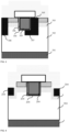
- FIG. 3 is a schematic structural diagram (cross-sectional view) of a trench-type MOSFET of Infineon.
- the MOSFET shown in FIG. 3 includes a heavily doped N-type substrate 301, a lightly doped N-type epitaxial layer 302 formed on the substrate 301, a P-type body region 303 formed on the epitaxial layer 302, a trench 304 formed by etching in the P-type body region 303, a gate oxide film 306 grown on the inner wall of the trench 304, and polysilicon 305 deposited on the gate oxide film 306.
- the trench-type MOSFET shown in FIG. 2 the trench-type MOSFET shown in FIG.
- the 3 further includes a heavily doped first P-type region 307 and a second P-type region 308 below the trench 304 to reduce the high electric field at the bottom of the trench 304, and the longitudinal depth of the P-type region is greater than the longitudinal depth of the P-type body region.
- FIG. 4 is a schematic structural diagram (cross-sectional view) of a trench-type MOSFET of Rohm.
- the MOSFET shown in FIG. 4 includes a heavily doped N-type substrate 401, a lightly doped N-type epitaxial layer 402 formed on the substrate 401, a P-type body region 403 formed on the epitaxial layer 402, a trench 406 formed by etching in the P-type body region 403, a gate oxide film 407 grown on the inner wall of the trench 406, and polysilicon 408 deposited on the gate oxide film 407.
- the trench-type MOSFET shown in FIG. 2 the trench-type MOSFET shown in FIG.
- first P-type region 404 and a second P-type region 405 further includes a heavily doped first P-type region 404 and a second P-type region 405 below the trench 406, to reduce the high electric field at the bottom of the trench 406, and the first P-type region 404 and the second P-type region 405 are respectively located on both sides of the trench 406, and the longitudinal depths of the first P-type region 404 and the second P-type region 405 are less than the longitudinal depth of the P-type body region in which the first P-type region 404 and the second P-type region 405 are located.
- the trench-type MOSFET structure shown in FIGS. 3 and 4 has high manufacturing costs and is difficult to control in the process.
- R N+ is the resistance of the source N+ diffusion region. Because the doping concentration of the N+ region is high, the resistance is very small. Therefore, this part of the resistance is negligible compared with other resistances that make up the drain-source on-resistance Rds( on ).
- R CH is the trench resistance, that is, the trench resistance under the gate.
- R CH is an important parameter that makes up the drain-source on-resistance Rds( on ). Changes in a ratio of the width to the length of the trench, a gate oxide thickness, and a gate voltage can all affect the change of R CH .
- R D is the drift region resistance, that is, the resistance of the epitaxial layer.
- the epitaxial layer is a high-resistance layer grown on the substrate to withstand high voltage. Under the action of external voltage, carriers drift in the drift region.
- the drift region resistance is the most important factor in determining the drain-source on-resistance Rds( on ). Therefore, the source-drain on-resistance Rds( on ) can be reduced by reducing the drift region resistance R D .
- R sub is the wafer substrate resistance, and this resistance value can be reduced by processes such as backside thinning.
- FIG. 5 is a schematic diagram of an angle relationship between a common silicon carbide crystal and a surface of a silicon carbide wafer in the silicon carbide wafer, that is, an angle relationship between a microscopic crystal and a macroscopic wafer.
- the X direction of the wafer surface and the Y direction perpendicular to the wafer surface (that is, the normal direction), as well as two mutually perpendicular crystallographic directions [0001] and [11 2 0] of the silicon carbide (4H-SiC) crystal are shown in the figure.
- a crystal is a structure composed of a large number of microscopic material units (such as atoms, ions, and molecules) arranged in an orderly manner according to certain rules. Therefore, the crystal usually has a specific shape. According to different shapes, the crystal axis, crystallographic direction, and crystal plane of the crystal can be defined. For example, at least two crystallographic directions of a silicon carbide (4H-SiC) crystal are defined as shown in the figure: the C-axis direction (that is, the [0001] direction) and the [11 2 0] direction. In the semiconductor industry, in order to make the crystal growth more stable during the production process, when cutting the wafer, the crystallographic direction shown in FIG.
- the angle is usually 4°; in addition, a projection of one crystallographic direction of the crystal, that is, the [11 2 0] direction on the wafer surface coincides with the X direction of the wafer.
- the angle is also ignored, and the crystallographic direction and mirror surface are directly used to refer to the direction of the wafer surface.
- FIG. 6 is a schematic structural diagram (cross-sectional view) of a trench-type power MOSFET with a non-axisymmetric P pillar obtained by ion implantation along the C axis when the silicon carbide wafer is cut in the direction shown in FIG. 5 .
- the trench-type power MOSFET shown in the figure includes a substrate 01, an epitaxial layer 02 formed on the substrate 01 by a process such as epitaxial growth, a P-type body region 04 formed on the epitaxial layer 02, and a trench 00 that penetrates the P-type body region 04 and that deeply extends into the epitaxial layer 02.
- the P pillar is located below the trench 00, buried in the epitaxial layer 02, and is usually formed by ion implantation.
- the crystallographic direction with the most obvious channel effect is usually selected as the direction of ion implantation.
- the direction of the C axis is the crystallographic direction with the most obvious channel effect.
- the C axis of silicon carbide is not perpendicular to the surface of the wafer, that is, in the structure shown in FIG. 6 , the P pillar 11 formed by ion implantation cannot be perpendicular to the surface of the wafer. That is, in the cross-sectional view of a unit cell as shown in FIG. 6 , the P pillar 11 cannot be symmetrical about the central axis of the unit cell.
- the person skilled in the art should know that, in the cross-sectional view shown in FIG. 6 , when the shape of the P pillar is an axisymmetric figure, the performance of the MOSFET device is the best.
- the cross-sectional view of the P pillar 11 obtained by ion implantation according to the prior art is a parallelogram as shown in FIG. 6 , which is asymmetrical about the central axis of the unit cell, and this easily leads to a low breakdown voltage of the MOSFET device.
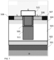
- FIG. 7 is a schematic diagram of a cross section of a trench gate power MOSFET structure according to some embodiments of the present application.
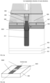
- FIG. 8a is a three-dimensional schematic diagram of the MOSFET shown in FIG. 7 at a 45° top view according to some embodiments of the present application.
- FIG. 8b is a schematic diagram of a mask pattern of a P-pillar connector 505 in FIG. 8a during the manufacturing process.
- the trench gate power MOSFET provided by the present invention includes a power MOSFET having a trench gate and super junction (or quasi-super junction) structure.
- a wide bandgap semiconductor substrate is a silicon carbide material
- the first conductivity type is N-type
- the second conductivity type is P-type
- the second conductivity-type pillar is a P pillar
- the first ion is an aluminum ion
- a substrate 501 is a substrate of a wide bandgap semiconductor having a first conductivity type.
- the substrate 501 can be a heavily doped N-type silicon carbide substrate.
- Lightly doped N-type first epitaxial layer 502 and second epitaxial layer 503 are sequentially grown on the substrate 501 by an epitaxial growth process.
- the first epitaxial layer 502 is located below the second epitaxial layer 503, the thickness of the first epitaxial layer 502 is less than the thickness of the second epitaxial layer 503, and the doping concentration of the first epitaxial layer 502 is less than the doping concentration of the second epitaxial layer 503.
- the N-type doping concentration of the first epitaxial layer 502 is between 1E14 atoms/cm 2 (atoms per square centimeter) and 2E16 atoms/cm 2 , and the thickness of the first epitaxial layer 502 is between 0.2 ⁇ m and 40 ⁇ m; the N-type doping concentration of the second epitaxial layer 503 is between 2E15 atoms/cm 2 and 2E17 atoms/cm 2 , and the thickness of the second epitaxial layer 503 is between 2 ⁇ m and 200 ⁇ m. It can be understood that the thickness and doping concentration of the first epitaxial layer 502 and the thickness and doping concentration of the second epitaxial layer 503 can be determined according to the withstand voltage rating required by the device. In this embodiment, the two epitaxial layers with different doping concentrations can be used to form a quasi-super junction device to enhance avalanche tolerance.
- the wide bandgap semiconductor substrate is a silicon carbide material, which is exemplary and not restrictive.
- the wide bandgap semiconductor substrate can further be other wide bandgap semiconductor materials, such as gallium nitride and aluminum nitride.
- the difference in selecting different substrate materials is that different trench setting directions and ion implantation directions are selected based on the different crystal orientations of different wafers (bodies).
- the impurities doped in the N-type doped first epitaxial layer 502 and the second epitaxial layer 503 can be nitrogen or phosphorus, or other N-type impurities.
- a P body region 504 is located above the second epitaxial layer 503, and can be formed by implanting ions of a conductivity type different from the substrate 501, the first epitaxial layer 502 and the second epitaxial layer 503, such as P-type ions, into the upper end of the second epitaxial layer 503.
- a P-pillar connector 505 is formed in the P body region 504 (P body region) and the second epitaxial layer 503 by an ion implantation process.
- a mask pattern 5051 indicating the P-pillar connector 505 is first formed on the upper surface of the P body region 504 by a photolithography mask process, as shown in FIG. 8b .
- the mask pattern is symmetrical about the central axis of the upper surface of the P body region 504 (see FIG. 8b ).
- P-type impurities are implanted in the region toward the P body region 504 and the second epitaxial layer 503 by an ion implantation process, thereby forming a columnar P-pillar connector 505.
- the connection between the P-pillar 511 and the P-body region 504 is implemented by using the P-pillar connector 505, so that the P-pillar 511 generated in the subsequent steps is electrically connected to the P-body region 504, and electrically floating does not occur in any working state.
- the depth of the P-pillar connector 505 needs to start from the upper surface of the P-body region 504 and extend deeply into the second epitaxial layer 503.
- the P-pillar 511 buried in the second epitaxial layer 503 can be electrically connected to the horizontal (referring to the horizontal in FIGS. 7 , 8a, and 8b ) P-body region 504 through the vertical (referring to the vertical in FIGS. 7 and 8a, 8b ) P-pillar connector 505.
- the ions are continuously implanted above the P-body region 504 (including the P-pillar connector 505) to form an ohmic contact resistance portion.
- N-type heavily doped impurities are implanted into the middle section of the P body region 504, that is, the portion including the P-pillar connector 505, to obtain a N-type heavily doped region 506, that is, the portion marked as S in FIG. 7 , so as to form a lower source ohmic contact resistance.
- P-type heavily doped impurities are implanted into the two ends of the P body region 504, that is, the positions connected to the two ends of the N-type heavily doped region 506, to obtain a first P-type heavily doped region 507 and a second P-type heavily doped region 508, so as to form a lower P body (that is, the P body region 504) ohmic contact resistance.
- a hard mask layer pattern 5002 for processing a trench 500 is formed on both sides of the central axis of the surface of the P body region 504.
- the mask pattern is discontinuous along the central axis, but is complementary to a mask pattern 5051 of the P-pillar connector 505.
- the P body region 504 and a part of the second epitaxial layer 503 under the hard mask layer pattern 5002 of the trench 500 are etched away to form the trench 500, while the P-pillar connector 505 under the mask pattern 5051 of the P-pillar connector 505 is retained as a conductor for electrical connection between the P pillar 511 and the P body region 504.
- the composition of the hard mask layer may be silicon dioxide or nickel. It is understood that in other embodiments, the composition of the hard mask layer may be other elements or compounds.
- the bottom 5001 of the trench 500 is located in the second epitaxial layer 503.
- the ratio of the depth to the width of the trench 500 may range from 1:1 to 5:1.
- the width of the trench 500 is 0.4 ⁇ m and the depth is 1.2 ⁇ m.
- the ratio of the depth to the width of the trench 500 is 3:1. It is understood that in the illustrated embodiment, the width and the depth of the trench 500 are exemplary and not restrictive. In other embodiments of the present application, the width and the depth of the trench 500 may be other values.
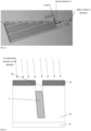
- the direction of the trench 500 is further illustrated below with reference to FIGS. 9a and 9b .
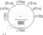
- a first pattern 72 and a second pattern 72' in FIGS. 9a and 9b are used to illustrate the positional relationship between the trench and the wafer 71.
- the shaded part is used to illustrate the trench 500, especially to illustrate the relationship between the length direction of the trench 500 and the crystal plane of the wafer 71.
- the surface of the wafer 71 shows multiple crystallographic directions (shown in square brackets) and crystal planes (shown in round brackets). According to the above description, it can be learned that, the surface of the silicon carbide wafer and the axial direction of the silicon carbide crystal are not at right angles.
- the directions of the wafer surface in the figure are actually the projections of the crystallographic directions of the silicon carbide crystal on the wafer surface.
- the crystallographic directions of the crystal are usually used to refer to the directions of the wafer surface.
- trenches 500 can be formed by etching on a wafer 71, and the directions of these trenches are the same.
- the trench is formed by etching in the direction shown in FIG. 9b by default, that is, the length direction of the trench is perpendicular to the crystal plane (1 1 00), as shown in the second pattern 72' in FIG. 9b .
- such a trench direction is the fundamental reason for the appearance of the parallelogram P pillar shown in FIG. 6 .
- the default trench setting direction in the industry is adjusted, so that the length direction of the trench is parallel to a projection of a selected crystallographic direction of a wafer (crystal) on the wafer surface.
- the C axis is both a crystallographic direction with an obvious channel effect and a crystallographic direction with the smallest deviation angle from the wafer normal in the current SiC wafer manufacturing method
- the trench setting direction of the present application needs to ensure that the length direction of the trench is parallel to the plane formed by the C axis and the wafer normal, so that the implantation along the C axis does not cause a shielding effect due to the influence of the trench sidewall and the mask.
- the selected crystallographic direction is the crystallographic direction with the most obvious channel effect among all crystallographic directions of the wafer, that is, the direction in which the greatest depth that can be achieved during ion implantation.
- the projection direction of the C axis on the wafer surface is selected. This change is conducive to the formation of symmetrical P pillars during subsequent ion implantation.
- the symmetrical P pillars 511 are formed when ions are implanted along the C axis (penetrating the paper plane and towards the outside).
- FIG. 10 later.
- ions are implanted into the bottom of the trench 500, and a P pillar 511 with a symmetrical cross-sectional shape can be obtained.
- aluminum ions are implanted into the bottom region of the trench 500 along the C-axis direction of silicon carbide (for 4H-SIC, the angle between the ion implantation direction and the normal direction of the 4H-SIC wafer is 4 degrees) with a first energy of 500kev to 1500kev and a first dose of 5E13 atoms/cm 2 to 5E14 atoms/cm 2 , and a second energy of 50kev to 300kev and a second dose of 5E12 atoms/cm 2 to 5E13 atoms/cm 2 , to implement deep uniform doping in silicon carbide to form a P pillar 511.
- silicon carbide for 4H-SIC, the angle between the ion implantation direction and the normal direction of the 4H-SIC wafer is 4 degrees
- the depth of the P pillar 511 is not less than 50% of the thickness of the second epitaxial layer 503 located below the bottom of the trench 500, the P pillar 511 is located in the second epitaxial layer 503, and the P pillar 511 and the N-type lightly doped second epitaxial layer 503 form a quasi-super junction structure. In this way, the P pillar 511 and the P body region 504 are connected in the width direction.
- the P-pillar connector 505 can also be formed by implanting ions into the sidewalls of the trench 500 after the trench 500 is formed by etching.
- the trench 500 is formed by continuously etching along the central axis of the unit cell, rather than by intermittently etching as shown in FIG. 8b .
- the etching depth penetrates the P-body region 504 and reaches the second epitaxial layer 503.
- ions are implanted into the sidewalls of the trench 500, so as to form P-pillar connectors 505 with a certain thickness on both sidewalls.
- the depth of these P-pillar connectors 505 is at least the same as the depth of the trench 500, so that the P-pillar connectors 505 can be electrically connected to the subsequently generated P-pillars 511 (the P-pillars 511 are generated at the bottom of the trench 500 by an ion implantation process and are connected to the bottom of the trench 500).
- the P-pillar connectors 505 can be electrically connected to the subsequently generated P-pillars 511 (the P-pillars 511 are generated at the bottom of the trench 500 by an ion implantation process and are connected to the bottom of the trench 500).
- the electrical connection between the P-body region 504 and the P-pillar 511 can be effectively implemented by using the P-pillar connector 505.
- FIG. 10 is a schematic diagram of the XYZ coordinate system on the upper surface of the wafer, in which the X direction and the Y direction are parallel to the wafer surface, and the Z direction is perpendicular to the wafer surface.
- FIG. 10 further shows multiple crystallographic directions and crystal planes of the silicon carbide crystal.
- the crystallographic direction schematic diagram is slightly deflected to show that there is an angle between the crystal and the wafer.
- a crystal plane (1 1 00) of silicon carbide is parallel to the XY plane
- a projection [11 2 0]x of a crystallographic direction [11 2 0] on the wafer surface is parallel to the X axis
- a projection Cy of the C axis on the YZ plane is parallel to the Y axis.
- the default trench direction in the industry is rotated by 90°, so that the length direction of the trench is shown in FIG. 9a , that is, the length direction of the trench is parallel to the X axis.
- the ions implanted along the C axis can be understood as being implanted along the Y axis (that is, the Cy direction perpendicular to the wafer) and along the X axis (that is, the [11 2 0] x direction parallel to the wafer).
- the X direction is the length direction of the trench, and the implantation of ions along this direction does not affect the cross-sectional shape of the P pillar 511 in the width direction of the trench 500.
- the range of ion implantation does not exceed the expected range.
- the P pillar 511 can form a symmetrical approximately rectangular structure. Compared with the prior art shown in FIG. 9b , the stability and reliability of the trench MOSFET can be improved in the present invention.
- the withstand voltage can be improved by the trench-type MOSFET of the present application.
- the doping concentration of the second epitaxial layer 503 can be reduced by the sufficiently deep P pillar 511, and the drift region resistance R D can be reduced, so that the on-resistance Rds( on ) is reduced.
- the implantation times, and corresponding energies and dose values of aluminum ions (such as Al-27) implanted into silicon carbide are exemplary and not restrictive. In other embodiments of the present application, the implantation times, corresponding energies and doses can be selected according to the required implantation depth.
- the implantation of aluminum ions (such as Al-27) from the C-axis direction of the 4H-SIC wafer here is exemplary and not restrictive.
- other ions whose conductivity type is P-type can be implanted into the second epitaxial layer along the crystallographic direction of another wide bandgap semiconductor, to implement a greater implantation depth with lower implantation energy by utilizing the crystal trench effect.
- the embodiment of the present application further provides a power MOSFET with a trench gate super junction structure (not shown), and the structure and preparation method of with a trench gate super junction structure are similar to the power MOSFET with a trench gate quasi-super junction structure described above.
- the only difference is as follows: Only a single epitaxial layer is needed by the MOSFET with a trench gate super junction structure during the preparation process, and the depth of the P pillar formed therein is not less than 50% of the thickness of the epitaxial layer located in the region below the bottom of the trench, so that the P pillar and the epitaxial layer form a super junction structure.
- the depth of the P pillar formed therein is not less than 50% of the thickness of the epitaxial layer located in the region below the bottom of the trench, so that the P pillar and the epitaxial layer form a super junction structure.
- FIG. 11 is a schematic flow diagram of a method for manufacturing a trench gate power MOSFET according to some embodiments of the present application. Specifically, as shown in FIG. 11 , the method for manufacturing a trench gate power MOSFET of the present application includes the following steps:
- the length direction of the trench is set to a direction perpendicular to the crystal plane (11 2 0) of the wafer 71 as shown in FIG. 9a , that is, the length direction of the trench is parallel to the crystallographic direction [11 2 0] (or more accurately, parallel to a projection of the crystallographic direction [11 2 0] on the wafer), but is not set to the direction shown in FIG. 9b .
- a P-pillar connector 505 can be formed between the bottom 5001 of the trench 500 and the P body region 504 by ion implantation.
- the P-pillar connector 505 is formed first. This can be understood with reference to FIGS. 8a and 8b .
- a region of a mask pattern 5051 of the P-pillar connector 505 as shown in the figure is prepared on both sides of the central axis (as shown in FIG. 8b ) of the upper surface of the P body region 504, and then in this region, P-type ions are implanted into the P body region 504 and the second epitaxial layer 503 to obtain the P-pillar connector 505.
- the depth of ion implantation should be greater than the depth of the trench 500, that is, the depth should reach the region of the P pillar 511, so that the electrical connection between the P body region 504 and the P pillar 511 formed in the subsequent process can be implemented by using the P-pillar connector 505.
- the trench 500 is formed in the P body region 504 and the second epitaxial layer 503 by etching according to the region of the hard mask layer pattern 5002 for processing the trench shown in FIG. 8b , and the depth and width of the trench can be controlled.
- the position of the mask pattern 5051 of the P-pillar connector 505 shown in FIG. 8b can be located at any position of the central axis, or there can be multiple mask patterns 5051 in a unit cell, and similar settings are not described herein.
- the body region can be etched by a dry etching technology to form a trench. In some embodiments, the body region can be etched by a wet etching technology to form a trench. It can be understood that the trench can be formed by dry etching or wet etching according to an actual situation. This is not limited herein.
- ion implantation can be performed downward at the connection between the P-pillar connector 505 and the bottom of the trench 500, so that the P-pillar connector 505 and the P-pillar 511 formed in the subsequent process can be more reliably electrically connected.
Landscapes
- Electrodes Of Semiconductors (AREA)
Applications Claiming Priority (2)
| Application Number | Priority Date | Filing Date | Title |
|---|---|---|---|
| CN202210888034.3A CN115084236B (zh) | 2022-07-27 | 2022-07-27 | 沟槽栅功率mosfet及其制造方法 |
| PCT/CN2023/103303 WO2024021977A1 (zh) | 2022-07-27 | 2023-06-28 | 沟槽栅功率mosfet及其制造方法 |
Publications (2)
| Publication Number | Publication Date |
|---|---|
| EP4528818A1 true EP4528818A1 (de) | 2025-03-26 |
| EP4528818A4 EP4528818A4 (de) | 2025-08-27 |
Family
ID=83243112
Family Applications (1)
| Application Number | Title | Priority Date | Filing Date |
|---|---|---|---|
| EP23845190.0A Pending EP4528818A4 (de) | 2022-07-27 | 2023-06-28 | Graben-gate-leistungs-mosfet und herstellungsverfahren dafür |
Country Status (6)
| Country | Link |
|---|---|
| US (1) | US12356679B2 (de) |
| EP (1) | EP4528818A4 (de) |
| JP (1) | JP7793809B2 (de) |
| KR (1) | KR102813923B1 (de) |
| CN (1) | CN115084236B (de) |
| WO (1) | WO2024021977A1 (de) |
Families Citing this family (3)
| Publication number | Priority date | Publication date | Assignee | Title |
|---|---|---|---|---|
| CN115084236B (zh) | 2022-07-27 | 2022-11-22 | 上海瞻芯电子科技有限公司 | 沟槽栅功率mosfet及其制造方法 |
| CN119277803B (zh) * | 2024-10-08 | 2026-02-03 | 上海瞻芯电子科技股份有限公司 | 碳化硅ldmos结构的形成方法、碳化硅ldmos结构及碳化硅ldmos器件 |
| CN119835982B (zh) * | 2025-03-14 | 2025-07-01 | 上海瞻芯电子科技股份有限公司 | 一种沟槽栅功率mosfet的结构及沟槽栅功率mosfet制造方法 |
Family Cites Families (25)
| Publication number | Priority date | Publication date | Assignee | Title |
|---|---|---|---|---|
| JP2009302510A (ja) * | 2008-03-03 | 2009-12-24 | Fuji Electric Device Technology Co Ltd | トレンチゲート型半導体装置およびその製造方法 |
| JP2009302436A (ja) * | 2008-06-17 | 2009-12-24 | Denso Corp | 炭化珪素半導体装置の製造方法 |
| CN102396070A (zh) * | 2009-04-13 | 2012-03-28 | 罗姆股份有限公司 | 半导体装置及半导体装置的制造方法 |
| JP5699878B2 (ja) * | 2011-09-14 | 2015-04-15 | 住友電気工業株式会社 | 炭化珪素半導体装置およびその製造方法 |
| JP6299102B2 (ja) | 2012-08-07 | 2018-03-28 | 株式会社デンソー | 炭化珪素半導体装置およびその製造方法 |
| CN104969357B (zh) * | 2013-02-05 | 2019-02-01 | 三菱电机株式会社 | 绝缘栅型碳化硅半导体装置及其制造方法 |
| CN105632931B (zh) * | 2014-11-04 | 2020-04-28 | 台湾积体电路制造股份有限公司 | 半导体器件的制造方法及半导体器件 |
| JP6569216B2 (ja) | 2014-12-22 | 2019-09-04 | 日産自動車株式会社 | 絶縁ゲート型半導体装置及びその製造方法 |
| US20170338302A1 (en) * | 2016-05-23 | 2017-11-23 | Infineon Technologies Ag | Power Semiconductor Device with Charge Balance Design |
| US11075264B2 (en) * | 2016-05-31 | 2021-07-27 | Cree, Inc. | Super junction power semiconductor devices formed via ion implantation channeling techniques and related methods |
| DE102016111998B4 (de) * | 2016-06-30 | 2024-01-18 | Infineon Technologies Ag | Ausbilden von Elektrodengräben unter Verwendung eines gerichteten Ionenstrahls und Halbleitervorrichtung mit Graben-Elektrodenstrukturen |
| US20190198622A1 (en) * | 2016-08-31 | 2019-06-27 | Sumitomo Electric Industries, Ltd. | Silicon carbide semiconductor device and method for manufacturing same |
| JP7081087B2 (ja) * | 2017-06-02 | 2022-06-07 | 富士電機株式会社 | 絶縁ゲート型半導体装置及びその製造方法 |
| DE112018002873T5 (de) | 2017-06-06 | 2020-02-27 | Mitsubishi Electric Corporation | Halbleitereinheit und leistungswandler |
| JP7259215B2 (ja) * | 2018-06-01 | 2023-04-18 | 富士電機株式会社 | 絶縁ゲート型半導体装置及び絶縁ゲート型半導体装置の製造方法 |
| US10580878B1 (en) * | 2018-08-20 | 2020-03-03 | Infineon Technologies Ag | SiC device with buried doped region |
| DE102019114312A1 (de) * | 2019-05-28 | 2020-12-03 | Infineon Technologies Ag | Siliziumcarbid-vorrichtung mit kompensationsgebiet und herstellungsverfahren |
| IT201900013416A1 (it) * | 2019-07-31 | 2021-01-31 | St Microelectronics Srl | Dispositivo di potenza a bilanciamento di carica e procedimento di fabbricazione del dispositivo di potenza a bilanciamento di carica |
| JP7263178B2 (ja) * | 2019-08-02 | 2023-04-24 | 株式会社東芝 | 半導体装置、インバータ回路、駆動装置、車両、及び、昇降機 |
| CN111276540A (zh) * | 2020-01-13 | 2020-06-12 | 上海瞻芯电子科技有限公司 | 沟槽栅功率mosfet及其制造方法 |
| CN111326567A (zh) * | 2020-03-06 | 2020-06-23 | 上海瞻芯电子科技有限公司 | 超级结的制造方法及其超级结肖特基二极管 |
| EP3930006A1 (de) * | 2020-06-24 | 2021-12-29 | Infineon Technologies AG | Halbleiterbauelement mit trench-gate-struktur und eingelassener abschirmungsregion und verfahren zur herstellung |
| CN111769156B (zh) * | 2020-07-02 | 2024-07-12 | 瑞能半导体科技股份有限公司 | 碳化硅沟槽栅晶体管及其制造方法 |
| JP7588342B2 (ja) | 2020-12-11 | 2024-11-22 | 株式会社東芝 | 半導体装置、インバータ回路、駆動装置、車両、及び、昇降機 |
| CN115084236B (zh) * | 2022-07-27 | 2022-11-22 | 上海瞻芯电子科技有限公司 | 沟槽栅功率mosfet及其制造方法 |
-
2022
- 2022-07-27 CN CN202210888034.3A patent/CN115084236B/zh active Active
-
2023
- 2023-06-28 JP JP2024552149A patent/JP7793809B2/ja active Active
- 2023-06-28 KR KR1020247039203A patent/KR102813923B1/ko active Active
- 2023-06-28 EP EP23845190.0A patent/EP4528818A4/de active Pending
- 2023-06-28 US US18/869,453 patent/US12356679B2/en active Active
- 2023-06-28 WO PCT/CN2023/103303 patent/WO2024021977A1/zh not_active Ceased
Also Published As
| Publication number | Publication date |
|---|---|
| US20250169129A1 (en) | 2025-05-22 |
| WO2024021977A1 (zh) | 2024-02-01 |
| CN115084236B (zh) | 2022-11-22 |
| US12356679B2 (en) | 2025-07-08 |
| CN115084236A (zh) | 2022-09-20 |
| JP7793809B2 (ja) | 2026-01-05 |
| JP2025511481A (ja) | 2025-04-16 |
| KR20240173637A (ko) | 2024-12-12 |
| EP4528818A4 (de) | 2025-08-27 |
| KR102813923B1 (ko) | 2025-05-27 |
Similar Documents
| Publication | Publication Date | Title |
|---|---|---|
| US11837629B2 (en) | Power semiconductor devices having gate trenches and buried edge terminations and related methods | |
| EP4528818A1 (de) | Graben-gate-leistungs-mosfet und herstellungsverfahren dafür | |
| EP0975024B1 (de) | Halbleitervorrichtung mit Schichten von abwechselnden Leitfähigkeitstypen und deren Herstellungsverfahren | |
| US20190304787A1 (en) | Method of manufacturing silicon carbide semiconductor device | |
| US5298442A (en) | Trench DMOS power transistor with field-shaping body profile and three-dimensional geometry | |
| US9443972B2 (en) | Semiconductor device with field electrode | |
| CN103730372B (zh) | 一种可提高器件耐压的超结制造方法 | |
| KR101802419B1 (ko) | 트렌치형 필러 옥사이드를 이용한 탄화규소 슈퍼정션 모스펫 및 그 제조방법 | |
| US8343841B2 (en) | Method for fabricating a semiconductor device | |
| CN111276540A (zh) | 沟槽栅功率mosfet及其制造方法 | |
| EP4256616A1 (de) | Finfet-leistungshalbleiterbauelemente | |
| WO2004088717A2 (en) | Superjunction device and method of manufacture therefore | |
| EP3682467B1 (de) | Verfahren zur herstellung eines p-dotierten gitters in einer n-dotierten sic-schicht | |
| US20240429272A1 (en) | Silicon carbide semiconductor devices with superjunctions | |
| CN222088608U (zh) | 功率开关器件结构 | |
| CN222088614U (zh) | 一种功率开关器件结构 | |
| US20250359142A1 (en) | Method for producing a semiconductor device and semiconductor device | |
| CN121645957A (zh) | 一种半导体器件结构及其制备方法 | |
| CN121692725A (zh) | 沟槽型碳化硅mosfet器件及其制备方法 | |
| CN121285021A (zh) | 一种高鲁棒性的超结SiC MOSFET器件及制备方法 | |
| CN119421450A (zh) | 一种沟槽型mosfet器件 | |
| CN120282497A (zh) | 基于碳化硅材料的半超结型场效应晶体管及其制造工艺 |
Legal Events
| Date | Code | Title | Description |
|---|---|---|---|
| STAA | Information on the status of an ep patent application or granted ep patent |
Free format text: STATUS: THE INTERNATIONAL PUBLICATION HAS BEEN MADE |
|
| PUAI | Public reference made under article 153(3) epc to a published international application that has entered the european phase |
Free format text: ORIGINAL CODE: 0009012 |
|
| STAA | Information on the status of an ep patent application or granted ep patent |
Free format text: STATUS: REQUEST FOR EXAMINATION WAS MADE |
|
| 17P | Request for examination filed |
Effective date: 20241220 |
|
| AK | Designated contracting states |
Kind code of ref document: A1 Designated state(s): AL AT BE BG CH CY CZ DE DK EE ES FI FR GB GR HR HU IE IS IT LI LT LU LV MC ME MK MT NL NO PL PT RO RS SE SI SK SM TR |
|
| REG | Reference to a national code |
Ref country code: DE Ref legal event code: R079 Free format text: PREVIOUS MAIN CLASS: H01L0029060000 Ipc: H01L0021040000 |
|
| A4 | Supplementary search report drawn up and despatched |
Effective date: 20250724 |
|
| RIC1 | Information provided on ipc code assigned before grant |
Ipc: H01L 21/04 20060101AFI20250718BHEP Ipc: H10D 62/10 20250101ALI20250718BHEP Ipc: H10D 30/01 20250101ALI20250718BHEP Ipc: H10D 30/66 20250101ALI20250718BHEP Ipc: H10D 62/832 20250101ALI20250718BHEP Ipc: H10D 62/40 20250101ALI20250718BHEP |
|
| DAV | Request for validation of the european patent (deleted) | ||
| DAX | Request for extension of the european patent (deleted) |