EP4517844A1 - Lichtemittierendes element und verfahren zur herstellung davon - Google Patents
Lichtemittierendes element und verfahren zur herstellung davon Download PDFInfo
- Publication number
- EP4517844A1 EP4517844A1 EP23796236.0A EP23796236A EP4517844A1 EP 4517844 A1 EP4517844 A1 EP 4517844A1 EP 23796236 A EP23796236 A EP 23796236A EP 4517844 A1 EP4517844 A1 EP 4517844A1
- Authority
- EP
- European Patent Office
- Prior art keywords
- light emitting
- emitting device
- symmetry axis
- layer
- sides
- Prior art date
- Legal status (The legal status is an assumption and is not a legal conclusion. Google has not performed a legal analysis and makes no representation as to the accuracy of the status listed.)
- Pending
Links
Images


Classifications
-
- H—ELECTRICITY
- H10—SEMICONDUCTOR DEVICES; ELECTRIC SOLID-STATE DEVICES NOT OTHERWISE PROVIDED FOR
- H10H—INORGANIC LIGHT-EMITTING SEMICONDUCTOR DEVICES HAVING POTENTIAL BARRIERS
- H10H20/00—Individual inorganic light-emitting semiconductor devices having potential barriers, e.g. light-emitting diodes [LED]
- H10H20/80—Constructional details
- H10H20/81—Bodies
- H10H20/819—Bodies characterised by their shape, e.g. curved or truncated substrates
-
- H—ELECTRICITY
- H10—SEMICONDUCTOR DEVICES; ELECTRIC SOLID-STATE DEVICES NOT OTHERWISE PROVIDED FOR
- H10H—INORGANIC LIGHT-EMITTING SEMICONDUCTOR DEVICES HAVING POTENTIAL BARRIERS
- H10H20/00—Individual inorganic light-emitting semiconductor devices having potential barriers, e.g. light-emitting diodes [LED]
- H10H20/01—Manufacture or treatment
- H10H20/011—Manufacture or treatment of bodies, e.g. forming semiconductor layers
- H10H20/018—Bonding of wafers
-
- H—ELECTRICITY
- H10—SEMICONDUCTOR DEVICES; ELECTRIC SOLID-STATE DEVICES NOT OTHERWISE PROVIDED FOR
- H10H—INORGANIC LIGHT-EMITTING SEMICONDUCTOR DEVICES HAVING POTENTIAL BARRIERS
- H10H20/00—Individual inorganic light-emitting semiconductor devices having potential barriers, e.g. light-emitting diodes [LED]
- H10H20/01—Manufacture or treatment
- H10H20/021—Singulating, e.g. dicing
-
- H—ELECTRICITY
- H10—SEMICONDUCTOR DEVICES; ELECTRIC SOLID-STATE DEVICES NOT OTHERWISE PROVIDED FOR
- H10H—INORGANIC LIGHT-EMITTING SEMICONDUCTOR DEVICES HAVING POTENTIAL BARRIERS
- H10H20/00—Individual inorganic light-emitting semiconductor devices having potential barriers, e.g. light-emitting diodes [LED]
- H10H20/01—Manufacture or treatment
- H10H20/011—Manufacture or treatment of bodies, e.g. forming semiconductor layers
- H10H20/019—Removal of at least a part of a substrate on which semiconductor layers have been formed
Definitions
- the present invention relates to a light emitting device and a method for producing the same.
- micro-LED micro light emitting diode
- the EZ-PETAMP series, SQDP series, SQDP-G series, and SQRP series manufactured by Shine-Etsu Chemical Co., Ltd. have been developed, which can significantly reduce mounting costs by transferring micro-LEDs from a starting substrate to a donor substrate and mounting thereon by adhering chips to the donor substrate having a silicone film formed on synthetic quartz and irradiating an interface between the starting substrate and an epitaxial layer with ultraviolet laser to sublimate the interface.
- this method is effective for, e.g., a GaN-based LED formed on a sapphire substrate, but cannot be applied to, e.g., an AlGaInP-based LED formed on a GaAs substrate.
- Patent Document 1 discloses a technique of bonding a semiconductor epitaxial substrate and a temporary support substrate by thermocompression via a dielectric layer, and a technique of separating the temporary support substrate and the epitaxial functional layer by wet etching.
- the same step (EZ-PETAMP) as the structure of a GaN-based LED formed on the sapphire substrate can be performed.
- pixels that can display RGB colors can be formed.
- a display being a display device, is formed by using RGB light emitting devices, a large number of LEDs are required to be mounted, and thus, it is essential to minimize material cost per one die to suppress overall cost.
- Patent Document 1 discloses the technique of bonding the semiconductor epitaxial substrate and the temporary support substrate by thermocompression via the dielectric layer, and the technique of separating the temporary support substrate and the epitaxial functional layer by wet etching as described above, this technique is not about an optimal device form of the micro-LEDs bonded via BCB layer, etc., and a technique for reducing the material cost of LED itself is not disclosed in this prior technique.
- micro-LED mounting cost has been reduced by the above EZ-PETAMP step, a unit cost per micro-LED is required to be reduced.
- space efficiency of a conventional rectangular die is not high, and as long as the rectangular die shape is selected, a theoretical number of dice obtained from a wafer is uniquely determined when a light-emitting area is defined as constant. This is because when LEDs for mounting, accompanied by a transfer step, are formed, devices move vertically during transferring, and a gap (isolation width between devices) between the LED devices is required to match the tolerance of the movement.
- the area, including the device isolation width is the area required for the actual devices, and the isolation width between devices cannot be set to zero; consequently, the area, including the area of the LED devices themselves and the isolation width between devices, is the area required for device formation.
- Patent Document 2 As a technique for minimizing the isolation width between devices, a technique adopting the closest packed structure based on regular hexagons has been disclosed in Patent Document 2.
- the regular hexagonal shape is not sufficient as a die shape for micro-LEDs with moving and mounting.
- a device wiring method by a wire-bonding is not used because a die size is very small (e.g., less than 100 ⁇ m).
- a bump may be used in some cases, flip mounting, in which an electrode formed on the LED device and an electrode on a mounting substrate are directly bonded, is generally used.
- the only method to increase yield of the number of dice that can be produced from a single wafer is to narrow the isolation width between devices when the device area is determined, and there is no other way to increase the yield.
- the isolation width between devices is narrowed, the yield during moving and mounting is reduced; therefore, the method of increasing yield by narrowing and improving the isolation width between devices required for moving and transferring has a limit, and the method to increase the yield further has not been disclosed in the prior technique.
- An object of the present invention is to provide a method for producing a light emitting device in which the yield of the device per a single wafer is improved without decreasing the yield during moving and transferring.
- the present invention provides a method for producing a light emitting device to produce a plurality of light emitting devices, the method comprising the steps of:
- the light emitting device can be produced, which has the shape having the plane view shape of the line-symmetric hexagon, sides parallel to the symmetry axis, length of the parallel sides longer than that of the other sides, and the two vertex angles through which the symmetry axis passes being 90° or more and less than 180°.
- a yield of the light emitting device per a single wafer can be improved compared to that of a light emitting device having a rectangular plane view shape.
- the method can further comprise a step of bonding a transparent substrate to the epitaxial layer via a bonding material and removing the starting substrate.
- the starting substrate is not the transparent substrate
- transferring the epitaxial layer to the transparent substrate in this way allows the application of a technique that is supposed to be performed to the substrate with the light emitting device formed on the transparent substrate.
- the two vertex angles can be 90° or more and 120° or less.
- the yield of the light emitting device per a single wafer can be further improved.
- a distance between the two sides parallel to the symmetry axis can be 1 ⁇ m or more and 100 ⁇ m or less.
- the present invention is particularly effective for producing a micro-LED having a distance between parallel sides of 1 to 100 ⁇ m.
- the isolation groove is formed by an ICP dry etching method.
- the formation of the isolation groove by such an ICP dry etching method can be performed precisely and easily.
- the transparent substrate is any of sapphire, quartz, or glass.
- these substrates can be suitably used as the transparent substrate, particularly, the substrate having a high transmissiveness to a laser can be selected.
- the bonding material can be at least any of benzocyclobutene, fluororesin, or epoxy resin.
- an area ratio of the light emitting layer to the total area of the device having the light emitting layer can be increased; and by setting the length of the parallel sides longer than that of the other sides, generation of short circuit can be suppressed due to misalignment during mounting.
- the light emitting device may be bonded to a transparent substrate via a bonding material.
- the two vertex angles are 90° or more and 120° or less.
- an area ratio of the light emitting layer to the total area of the device having the light emitting layer can be further increased.
- a distance between the two sides parallel to the symmetry axis can be 1 ⁇ m or more and 100 ⁇ m or less.
- the present invention is particularly effective for applying to a micro-LED in which a distance between the sides parallel is 1 to 100 ⁇ m.
- the transparent substrate is any of sapphire, quartz, or glass.
- These substrates can be suitably used as the transparent substrate, particularly, can be selected so as to increase transmissiveness to a laser.
- the bonding material is at least any of benzocyclobutene, fluororesin, or epoxy resin.
- bonding materials can be suitably used as a bonding material.
- the light emitting device can be produced in which the shape of the device has the plane view shape of the line-symmetric hexagon, the sides parallel to the symmetry axis, length of the parallel sides longer than that of other sides, and two vertex angles through which the symmetry axis passes being 90° or more and less than 180°.
- the yield of the light emitting device per a single wafer can be improved compared to that of the rectangular device.
- the generation of short circuit can be suppressed due to misalignment during mounting.
- the vertex angle is 90° or more, the mechanical strength of the vertex portion of the triangular shape can be prevented from weakening, and cracking at the triangular shape can be suppressed.
- the inventive light emitting device by forming electrodes in the triangular portion of the hexagonal shape, including vertex potions through which the symmetry axis passes, the area ratio of the light emitting layer to the total area of the device having the light emitting layer can be increased; and by setting the length of the parallel sides longer than that of the other sides, generation of short circuit can be suppressed due to misalignment during mounting.
- the present inventor has earnestly studied the above problem and found out to form a shape of the light emitting device so as to have a specific hexagonal shape. This finding has led to the completion of the present invention.
- the present invention is a method for producing a light emitting device to produce a plurality of light emitting devices, the method comprising the steps of:
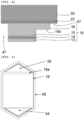
- the inventive light emitting device is a light emitting device, wherein the light emitting device has a shape having a plane view shape of a line-symmetric hexagon with a symmetry axis, two sides parallel to the symmetry axis, length of the two parallel sides longer than that of other four sides, and two vertex angles through which the symmetry axis passes being 90° or more and less than 180°.
- the first embodiment is an embodiment including a step of growing an epitaxial layer on a starting substrate, then bonding a transparent substrate to the epitaxial layer via a bonding material and removing the starting substrate.
- an epitaxial layer 18, including a light emitting layer, is grown on a starting substrate 11. More specifically, the step is as follows.
- an etching stop layer 12 is epitaxially grown on a first conductivity-type starting substrate 11 made of, e.g., GaAs.
- the etching stop layer 12 can be formed, for example, after laminating a first conductivity-type GaAs buffer layer, followed by growing a first conductivity-type GaInP first etching stop layer of, e.g., 0.1 ⁇ m, and, for example, a first conductivity-type GaAs second etching stop layer of, e.g., 0.1 ⁇ m.
- an epitaxial wafer 20 including an epitaxial layer 18 is provided in which, for example, a first conductivity-type AlGaInP first cladding layer 13 of a thickness of, e.g., 1.0 ⁇ m, for example, a non-doped AlGaInP active layer 14, for example, a second conductivity-type AlGaInP second cladding layer 15 of, e.g., 1.0 ⁇ m, a second conductivity-type GaInP intermediate layer (not shown) of, e.g., 0.1 ⁇ m, and further, for example, a second conductivity-type GaP window layer 16 of, e.g., a thickness of 6 ⁇ m are sequentially grown on the etching stop layer 12.
- the method can further include a step of bonding a transparent substrate 30 to the epitaxial layer 18 via a bonding material 25 and removing the starting substrate 11 as shown in FIGS 2 and 3 . More specifically, the step is as follows.
- the epitaxial wafer 20 is spin-coated thereon with benzocyclobutene (BCB), being a thermosetting bonding material, as a bonding material 25 and then by facing, superimposing, and thermo-compressing with, for example, a sapphire wafer (transparent substrate 30) which is a to-be-bonded wafer; and then a first epitaxial bonded substrate is produced, in which the epitaxial wafer 20 and the sapphire wafer (transparent substrate 30) are bonded via the BCB (bonding material 25).
- BCB benzocyclobutene
- a designed film thickness can be, for example, 0.6 ⁇ m, but not limited to this thickness, and the same effect can be obtained even when the thickness is equal to, or thicker or thinner than this thickness.
- Pressurizing and bonding can be performed under bonding conditions in this case, including, for example, a temperature of 200°C or more and 400°C or less and a pressure of 1.2 N/cm 2 or more.
- a material of the to-be-bonded substrate, as the transparent substrate 30 in this case is not limited to sapphire, but any material can be selected as long as flatness is guaranteed. Quartz or glass, etc., may be selected other than sapphire.
- the starting substrate 11 for example, GaAs starting substrate
- the etching stop layer 12 is also removed.
- the etching stop layer 12 includes the first etching stop layer and the second etching stop layer; first, the first etching stop layer is exposed by etching, then the etchant is switched to remove the second etching stop layer, and then the epitaxial layer 18 (first cladding layer 13 in epitaxial layer 18) can be exposed.
- a second epitaxial bonded substrate that retains only the double-hetero (DH) structure portion (first cladding layer 13, active layer 14, second cladding layer 15) and the window layer 16 can be produced ( FIG. 3 ).
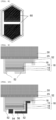
- an isolation groove 47 for device formation is formed in the light emitting layer (see FIG. 4 ).
- the formation of the isolation groove 47 is preferably formed by an ICP dry etching method because of simplicity and high precision. More specific methods are described, referring to FIGs 4 to 8 .
- a pattern is first formed by a photolithography method, as shown in FIG. 4 , and device isolation processing is performed by ICP (inductively coupled plasma).
- ICP inductively coupled plasma
- Gases used for ICP can be chlorine and argon.
- the ICP processing can be performed twice, including the device isolation step to expose the bonding material 25 layer (BCB layer) and the exposure step to expose the window layer 16 (GaP window layer).
- the case is not limited to such the case where the window layer 16 (GaP window layer) is exposed ( FIG. 4 ), and it is only required that the active layer 14 is isolated; and the same effect can be obtained when the second cladding layer 15 is exposed instead of the exposure of the window layer 16 (GaP window layer).
- FIG. 4 shows 18a as a region where an underlayer of the light emitting layer is exposed.
- FIG. 4 shows the case where the window layer 16 is exposed as the underlayer exposed region 18a.
- respective plane view shapes of a plurality of light emitting devices to be produced are a predetermined hexagonal shape as shown in FIGs 5 to 8 when the device isolation step (the step to form the isolation groove to the light emitting layer for the device formation) is performed.
- This hexagonal shape is a line-symmetric hexagon having a symmetry axis with two sides parallel to the symmetry axis, in which length of the two parallel sides is longer than that of the other four sides and two vertex angles through which the symmetry axis passes are 90° or more and less than 180°.
- the two vertex angles are preferably 90° or more and 120° or less.
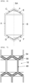
- the plurality of the light emitting devices to be produced are isolated by the isolation groove of a predetermined width, and the isolation groove is formed so as to arrange the plurality of light emitting devices without a gap via the isolation groove (see FIG. 7 ). Such an arrangement is similar to an arrangement which is referred to as a honeycomb structure when arranged in regular hexagons.
- FIG. 5 is the plane view shape of the epitaxial layer 18 having the light emitting layer being device-isolated by the isolation groove 47 through each step in FIGs 1 to 4 .
- a region indicated by reference sign 54 in FIG. 5 is a position of an upper electrode 54 described later
- a region indicated by reference sign 56 in FIG. 5 is a position of a lower electrode 56 described later.
- a triangle region around the lower electrode 56 (a region of reference sign 18a separated by a dashed line in the hexagon shown by a solid line) is the underlayer exposed region 18a shown in FIG. 4 .
- a dashed line outside the hexagon which is indicated by a solid line in FIG.
- FIG. 5 is a device isolation intermediate line 48.
- the device isolation intermediate line 48 indicates an intermediate line of the isolation groove 47 between respective light emitting layers isolated by the device isolation.
- FIG. 7 shows a state of the light emitting layers of FIG. 5 in a plurality of arrays (underlayer exposed region 18a is omitted from the drawings).
- the hexagonal shape shown in FIG. 6 corresponds to the shape of the light emitting layer in FIG. 5 .
- the hexagonal shape shown in FIG. 6 is the line-symmetric hexagon having a symmetry axis SA. Further, this hexagonal shape has two sides parallel to the symmetry axis SA (side A and side B), and the length of the two parallel sides (side A and side B) is longer than other four sides (side C, side D, side E, and side F). Moreover, two vertex angles ( ⁇ and ⁇ ) through which the symmetry axis SA passes are 90° or more and less than 180°.
- the light emitting device in the hexagonal shape identified in this way is further isolated by the isolation groove having the predetermined width as shown in FIG. 7 , and the isolation grooves are formed so as to arrange a plurality of light emitting devices without gaps via the isolation grooves.
- FIG. 8 shows a relation between the light emitting device shown in FIG. 5 and a position where a contact pad 60 is arranged.
- the light emitting device in the hexagonal shape specified as described above can be produced.
- the yield of the light emitting device per a single wafer can be improved compared to the rectangular light emitting device.
- the generation of short circuit can be suppressed due to misalignment during mounting.
- the vertex angle is 90° or more, the mechanical strength of the vertex portion of the triangular shape can be prevented from weakening, and cracking at the triangular shape portion can be suppressed.
- the two vertex angles ( ⁇ and ⁇ ) described above are preferably 90° or more and 120° or less.
- the vertex angles are preferably 90° or more and 120° or less.
- the yield of the light emitting device per a single wafer can be further improved.
- the area ratio of the light emitting layer to the total area of the device having the light emitting layer can be further increased.
- the vertex angle is smaller than 90°, the triangular portion protrudes too much and thus decreases the mechanical strength and, therefore, cannot withstand stress when electrically connected to mounting electrodes, and is prone to chipping and cracking in the protrusion.
- the vertex angle is 90° or more, such die breakage is unlikely to occur.
- a distance between the two sides (A and B) parallel to the symmetry axis SA is set to 1 ⁇ m or more and 100 ⁇ m or less; when a small light emitting device, i.e., a micro-LED, is produced, the present invention is particularly effective.
- a protective film 52 As the protective film 52, for example, SiO 2 can be used, but the film is not limited to SiO 2 , any material can be selected as long as the material can protect the end surface and has an insulating property. SiN x , titanium oxide, magnesium oxide, and the like can be selected.
- the electrode (upper electrode 54) in contact with the first conductivity-type layer (first cladding layer 13 in FIG. 10 ) and the electrode (lower electrode 56) in contact with the second conductivity-type layer (window layer 16 in FIG. 10 ) are formed, and then ohmic contact can be formed by performing heat treatment ( FIG. 10 ).
- the first conductivity-type as n-type and the second conductivity-type as p-type, and then to use a metal containing, for example, Au and Si for the electrode in contact with an n-type layer, and a metal containing, for example, Au and Be for the electrode in contact a P-type layer.
- the metal of the n-type electrode is not limited to Au and Si, and the same result can be obtained by using metals containing Au and Ge.
- the metal of the p-type electrode is not limited to Au and Be, and the same result can be obtained by using metals containing Au and Zn.
- This embodiment in which the devices with electrodes formed thereon are bonded via BCB, can be provided as a product for EZ-PETAMP step described above.
- a template substrate being a synthetic quartz substrate subjected to convex pattern processing thereon
- BCB is sublimated by laser irradiation from the to-be-bonded substrate side, and then the device is transferred from the to-be-bonded substrate to the template substrate.
- the transferred device is then re-transferred to a mounting substrate having a drive circuit to form an RGB display device.
- the devices When the device is transferred to the mounting substrate, the devices are transferred discretely in both the horizontal and vertical directions, as shown schematically in FIG. 11 . This is because a formation pitch of the micro-LED and that of the mounting side are generally different when forming the RGB display device.
- a first conductivity-type GaN buffer layer is grown on, e.g., a transparent sapphire starting substrate, then the epitaxial wafer is provided with a light-emitting device structure as the epitaxial functional layer in which, e.g., a first conductivity-type GaN first cladding layer having a thickness of 1.0 ⁇ m, e.g., a non-doped InGaN active layer, e.g., a second conductivity-type AlGaN second cladding layer having a thickness of 0.5 ⁇ m, e.g., and a second conductivity-type GaN window layer having a thickness of 6 ⁇ m are sequentially grown.
- a DH structure potion is sequentially grown from the first cladding layer to the second cladding layer.
- the step in which a pattern is subsequently formed by a photolithography method and then device isolation processing and exposure processing are performed by ICP is the same as that of the first embodiment.
- a protective film forming step and structure, as end surface processing, are the same as those of the first embodiment.
- electrodes are formed to form an ohmic contact. Unlike the first embodiment, Ti/Al/Ni/Au, etc., are used for the electrodes.
- a transferring method or a mounting method after the electrode formation is the same as in the first embodiment in that a laser is irradiated from a transparent substrate such as a sapphire substrate, but it is different from the first embodiment in which a GaN buffer layer portion is sublimated and delaminated instead of sublimating BCB.
- an epitaxial layer including a light-emitting layer, was grown on a starting substrate. Specifically, the following were implemented. To begin with, after laminating an n-type GaAs buffer layer on an n-type GaAs starting substrate 11, an etching stop layer 12 was formed thereon by forming an n-type GaInP first etching stop layer having a thickness of 0.1 ⁇ m and an n-type GaAs second etching stop layer having a thickness of 0.1 ⁇ m.
- An epitaxial wafer 20 was provided with a light emitting layer (light emitting device structure) as an epitaxial functional layer in which an n-type AlGaInP first cladding layer 13 having a thickness of 1.0 ⁇ m, a non-doped AlGaInP active layer 14, a p-type AlGaInP second cladding layer 15 having a thickness of 1.0 ⁇ m, and a p-type GaInP intermediate layer having a thickness of 0.1 ⁇ m (not shown), further, a p-type GaP window layer 16 having a thickness of 6 ⁇ m were sequentially grown on the etching stop layer 12 ( FIG. 1 ).
- a light emitting layer light emitting device structure
- the epitaxial wafer 20 is spin-coated thereon with benzocyclobutene (BCB) as a bonding material 25, and then by facing, superimposing, and bonding to a sapphire wafer, being a transparent substrate 30, under bonding conditions of 2 N/cm 2 and 250°C, a first epitaxial bonded substrate was produced ( FIG. 2 ).
- BCB benzocyclobutene
- a designed film thickness was 0.6 ⁇ m.
- the GaAs starting substrate 11 was removed by wet etching to expose the first etching stop layer, and then the etchant was switched to remove the second etching stop layer, thereby removing the etching stop layer 12. Consequently, the first cladding layer 13 was exposed to produce a second epitaxial bonded substrate ( FIG. 3 ).
- a pattern was formed by a photolithography method, and device isolation processing was performed by ICP.
- Gases used for ICP were chlorine and argon, and the ICP processing was performed twice, including the device isolation step to expose the BCB layer 25 and the exposure step to expose the GaP window layer 16 ( FIG. 4 ). Thereby, an isolation groove 47 for device formation was formed in the light emitting layer.
- a plane view shape of the devices was a shape of a line-symmetric hexagon having a symmetry axis SA with two sides parallel to the symmetry axis SA (side A and side B), in which length of the two parallel sides (side A and side B) was longer than that of other four sides (sides C to F) and two vertex angles ( ⁇ and ⁇ ) through which the symmetry axis SA passed were 120° ( FIGs 5 to 7 ).
- Concrete dimensions of the device were: a distance between the vertex portion (vertex angle ⁇ ) and the vertex portion (vertex angle ⁇ ) on the symmetry axis SA was 13.50 ⁇ m, a distance between the parallel side A and side B was 7.79 ⁇ m, and an area of one device isolated by the device isolation groove 47 was 87.64 ⁇ m 2 .
- Electrodes were provided in an isosceles triangle portion within the hexagonal shape (upper electrode 54 and lower electrode 56) as shown in FIG. 5 .
- ohmic contact electrodes described later were provided adjacent to an area having 120° degree angular shape (area including the vertex angle ⁇ and the vertex angle ⁇ shown in FIG. 6 ).
- a distance between the electrode and an outer edge portion of a die was determined by tolerance during photolithography, and in this Example, the tolerance was 0.25 ⁇ m.
- Each ohmic contact electrode area was 6.93 ⁇ m 2 , and a distance between the electrodes was 9.00 ⁇ m.
- the isolation width between the devices was set to 0.87 ⁇ m, and a shape portion indicated by a dashed line in FIG. 5 corresponded to an intermediate line between the devices (device isolation intermediate line 48).
- the area inside the dashed line was an area required for device production, and that area was 103.92 ⁇ m 2 with a width of 8.66 ⁇ m and a distance of 14.50 ⁇ m between the vertex portion to the vertex portion on the symmetry axis SA.
- FIG. 7 Each device in the hexagonal shape was arranged as shown in FIG. 7 , and each device shape included the vertex portions of the isosceles triangle. Thus, the devices arranged vertically were shifted by half a length from each other.
- FIG. 8 shows an arrangement of contact pads 60 with a mounting substrate provided on the device shown in FIG. 5 .
- An alignment tolerance at the time of contact pad 60 formation was 0.25 ⁇ m, and a width from an electrode edge portion (vertical direction in the drawing) was 4.00 ⁇ m, a clearance between the electrodes having a different polarity was 1.00 ⁇ m.
- a SiO 2 protective film 52 was formed as end surface processing ( FIG. 9 ). Subsequently, the electrode in contact with an n-type layer and the electrode in contact with a p-type layer (upper electrode 54 and lower electrode 56) were formed to form an ohmic contact by performing heat treatment ( FIG. 10 ).
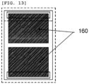
- a light emitting device was formed in the same way as in Example, except that a device isolation pattern was rectangular ( FIG. 12 ).
- a shape of the light emitting device had a distance of 11.25 ⁇ m in a major axis direction, a width of 7.79 ⁇ m in a minor axis direction, and an area of the device isolated by a device isolation groove was 87.64 ⁇ m 2 , which was the same as in Example.
- a distance between the electrodes (upper electrode 154 and lower electrode 156) and an outer edge portion of a device 118 was determined by tolerance during photolithography, but the tolerance was 0.25 ⁇ m as in Example. Note that FIG. 12 also shows an underlayer exposed region 118a. Each ohmic contact electrode area was 6.93 ⁇ m 2 as in Example, and a distance between the electrodes was 8.75 ⁇ m.
- the isolation width between devices was set to 0.87 ⁇ m, and an area required for a device production indicated by a dashed line (device isolation intermediate line 148) in FIG. 12 was 104.96 ⁇ m 2 with a width of 8.66 ⁇ m and a distance of 12.12 ⁇ m in a major axis direction.
- the area required for the device production in Comparative Example became larger than that of Example.
- FIG. 13 shows an arrangement of contact pads 160 with a mounting substrate provided on FIG. 12 .
- An alignment tolerance at the time of contact pad 160 formation was 0.25 ⁇ m, a width from an electrode edge portion (vertical direction in the drawing) was 4.00 ⁇ m, and a clearance between the electrodes having a different polarity was 0.75 ⁇ m.
- the clearance between the contact pads in Comparative Example was smaller than that in Example with the same design. When the clearance was shorter, a short circuit was prone to generate during mounting due to misalignment, thereby making a required alignment tolerance more stringent.
- the clearance between the electrodes was required to be set large enough to meet the alignment tolerance, and the die in Comparative Example needed to be longer in the major axis direction than that in Example to meet the alignment tolerance. Consequently, the required die area is necessarily larger than that of Example.
- the area of the light emitting device was set to the same as that in Example, but when making it consistent with the required tolerance necessary during mounting, it was impossible to design the die with the same size as in Comparative Example; the die needed to be long in the major axis direction, and the area required for a die formation necessarily needed to be designed to be larger than in Example.
- the clearance of the contact pads was set to 1.00 ⁇ m
- the same as Example the die was required to be extended by 0.25 ⁇ m from 11.25 ⁇ m to 11.50 ⁇ m in the major axis direction, and the die area required to achieve the same alignment as in Example was required to be increased by 2.2% from 87.64 ⁇ m 2 to 89.59 ⁇ m 2 .
- an area required for device production (corresponding to an area inside the device isolation intermediate line 148 indicated by the dashed line) increased by 2.9% from 104.96 ⁇ m 2 to 108.00 ⁇ m 2 .
- this area was 3.9% larger. Consequently, a die yield per a single wafer was lowered than that of Example.
- the width of the light emitting device is 7.79 ⁇ m, and a plane view area of the light emitting device is 87.64 ⁇ m 2 .
- a distance (width) to the intermediate line (device isolation intermediate line 48) of a distance to an adjacent device indicated by the dashed line is 0.43 ⁇ m (the distance to the adjacent die was 0.86 ⁇ m).
- the area required per one light emitting device is a region enclosed by the intermediate line (the region enclosed by the device isolation intermediate line 48 indicated by the dashed line).
- the area of the region enclosed by this device isolation intermediate line 48 is 103.92 ⁇ m 2 .
- the region enclosed by the device isolation intermediate line 148 is found to be 104.96 ⁇ m 2 when the areas of the light emitting devices are identical, and the design in Example has 1.00% smaller area than that in the rectangular case (Comparative Example).
- underlayers are exposed to form ohmic contact layers in both Example and Comparative Example (shown as underlayer exposed region 18a in FIG. 5 , and underlayer exposed region 118a in FIG. 12 ), the ohmic contact electrodes (lower electrode 56 and lower electrode 156 in Example and Comparative Example, respectively) are formed in contact with the exposed underlayers.
- the electrode areas in contact with the underlayers are standardized to 6.93 ⁇ m 2 , respectively.
- the electrode is triangular, and in FIG. 12 of Comparative Example, the electrode is rectangular.
- the vertical and horizontal distances from the edge of the device isolation are standardized to be 0.25 ⁇ m, which is the same rule in the examples described above.
- the light emitting layer remains in the region other than the area, which is cut off to expose the underlayer, and the area of the remaining light emitting layer contributes to effective light emitting.
- This area is 75.49 ⁇ m 2 in Example, and 74.55 ⁇ m 2 in Comparative Example, and thus a difference of about 1.25% is observed.
- Various characteristics of an LED are determined by a current density injected into the light emitting layer. The current density is determined by the area of the light emitting layer and the amount of electric power injected into the active layer; therefore, it is not the area of an entire die that determines the characteristics of the LED, but the area of the light emitting layer.
- an overall area of the light emitting device can be reduced compared to the conventional technique, and occupancy area required for production of the light emitting device can be reduced.
- the area of the light emitting layer portion is larger in Example when the die areas are standardized, and it is clear that the die area can be smaller than that of the die of the conventional technique when the technique of the present invention is used. Therefore, when this technique is applied by standardizing the light emitting layer area as in the conventional technique instead of the die area, the actions and effects of this technique become larger than the effect shown here. The same effect can be obtained when making the light emitting device area smaller by matching the light emitting layer areas instead of matching the light emitting device areas.
- the present description includes the following embodiments.
Landscapes
- Led Devices (AREA)
Applications Claiming Priority (2)
| Application Number | Priority Date | Filing Date | Title |
|---|---|---|---|
| JP2022073796A JP7243899B1 (ja) | 2022-04-27 | 2022-04-27 | 発光素子及びその製造方法 |
| PCT/JP2023/015765 WO2023210494A1 (ja) | 2022-04-27 | 2023-04-20 | 発光素子及びその製造方法 |
Publications (2)
| Publication Number | Publication Date |
|---|---|
| EP4517844A1 true EP4517844A1 (de) | 2025-03-05 |
| EP4517844A4 EP4517844A4 (de) | 2026-04-15 |
Family
ID=85685022
Family Applications (1)
| Application Number | Title | Priority Date | Filing Date |
|---|---|---|---|
| EP23796236.0A Pending EP4517844A4 (de) | 2022-04-27 | 2023-04-20 | Lichtemittierendes element und verfahren zur herstellung davon |
Country Status (5)
| Country | Link |
|---|---|
| EP (1) | EP4517844A4 (de) |
| JP (1) | JP7243899B1 (de) |
| CN (1) | CN119032430A (de) |
| TW (1) | TW202416356A (de) |
| WO (1) | WO2023210494A1 (de) |
Families Citing this family (1)
| Publication number | Priority date | Publication date | Assignee | Title |
|---|---|---|---|---|
| WO2025120744A1 (ja) * | 2023-12-05 | 2025-06-12 | 信越化学工業株式会社 | 転写方法、転写ユニット、リリースプレート、リリースプレート前駆基板、表示装置の製造方法、及び実装基板の製造方法 |
Family Cites Families (13)
| Publication number | Priority date | Publication date | Assignee | Title |
|---|---|---|---|---|
| JP3863962B2 (ja) * | 1997-03-25 | 2006-12-27 | シャープ株式会社 | 窒化物系iii−v族化合物半導体発光素子とその製造方法 |
| US6307218B1 (en) | 1998-11-20 | 2001-10-23 | Lumileds Lighting, U.S., Llc | Electrode structures for light emitting devices |
| JP3904585B2 (ja) | 2004-10-07 | 2007-04-11 | 昭和電工株式会社 | 半導体素子の製造方法 |
| JP5024722B2 (ja) * | 2005-06-06 | 2012-09-12 | 住友電気工業株式会社 | 窒化物半導体基板とその製造方法 |
| JPWO2009088084A1 (ja) * | 2008-01-11 | 2011-05-26 | ローム株式会社 | 半導体発光装置 |
| JP6156402B2 (ja) * | 2015-02-13 | 2017-07-05 | 日亜化学工業株式会社 | 発光装置 |
| JP6146460B2 (ja) | 2015-02-26 | 2017-06-14 | 日亜化学工業株式会社 | 発光素子 |
| JP6428467B2 (ja) | 2015-04-24 | 2018-11-28 | 日亜化学工業株式会社 | 発光素子 |
| JP6265175B2 (ja) | 2015-06-30 | 2018-01-24 | 日亜化学工業株式会社 | 半導体素子の製造方法 |
| JP6361645B2 (ja) * | 2015-12-22 | 2018-07-25 | 日亜化学工業株式会社 | 発光装置 |
| JP6431631B1 (ja) * | 2018-02-28 | 2018-11-28 | 株式会社フィルネックス | 半導体素子の製造方法 |
| JP2021027301A (ja) | 2019-08-08 | 2021-02-22 | 信越半導体株式会社 | 半導体基板の仮接合方法 |
| JP7200884B2 (ja) * | 2019-08-27 | 2023-01-10 | 信越化学工業株式会社 | 微小構造体の実装方法 |
-
2022
- 2022-04-27 JP JP2022073796A patent/JP7243899B1/ja active Active
-
2023
- 2023-04-20 CN CN202380036487.6A patent/CN119032430A/zh active Pending
- 2023-04-20 EP EP23796236.0A patent/EP4517844A4/de active Pending
- 2023-04-20 WO PCT/JP2023/015765 patent/WO2023210494A1/ja not_active Ceased
- 2023-04-24 TW TW112115077A patent/TW202416356A/zh unknown
Also Published As
| Publication number | Publication date |
|---|---|
| CN119032430A (zh) | 2024-11-26 |
| WO2023210494A1 (ja) | 2023-11-02 |
| JP7243899B1 (ja) | 2023-03-22 |
| EP4517844A4 (de) | 2026-04-15 |
| JP2023163011A (ja) | 2023-11-09 |
| TW202416356A (zh) | 2024-04-16 |
Similar Documents
| Publication | Publication Date | Title |
|---|---|---|
| US11791446B2 (en) | Micro-device with strengthened connecting layers | |
| CN109390437B (zh) | 微型发光二极管装置及其制作方法 | |
| CN104022216B (zh) | 发光装置 | |
| TWI750650B (zh) | 用於表面貼裝微型led流體組裝的發光顯示基板及製備方法 | |
| TWI469382B (zh) | 發光二極體結構與元件以及其製造方法 | |
| US12538610B2 (en) | Method for manufacturing a micro LED display using parallel mass transport | |
| EP2953171A1 (de) | Optisches halbleiterbauelement und verfahren zur herstellung eines optischen halbleiterbauelements | |
| WO2018163713A1 (ja) | 発光素子及びその製造方法 | |
| CN111477726A (zh) | 用于流体组装的平面表面贴装微型led及其制备方法 | |
| EP4517844A1 (de) | Lichtemittierendes element und verfahren zur herstellung davon | |
| KR20070028364A (ko) | 반도체 발광 다이오드상의 반사층 제조 | |
| TW201532303A (zh) | 應力誘導裁切半導體裝置之方法 | |
| CN114303236A (zh) | 多芯片承载结构 | |
| KR101128261B1 (ko) | 전공정이 웨이퍼 레벨로 제조된 led 패키지 및 그 제조방법 | |
| EP4571855A1 (de) | Verfahren zur herstellung eines gebondeten wafers für mikro-leds | |
| KR20190119880A (ko) | 반도체 발광소자 패널을 제조하는 방법 | |
| KR20200082872A (ko) | 마이크로 반도체 발광소자 제조방법 | |
| US20050127388A1 (en) | Light-emitting device and forming method thereof | |
| US12356780B2 (en) | Display device and manufacturing method thereof | |
| KR100889568B1 (ko) | 질화물계 발광소자 및 그 제조방법 | |
| KR100661717B1 (ko) | 알루미늄 버퍼층을 이용한 발광 다이오드 제조방법 | |
| KR100335796B1 (ko) | 사파이어 기판위에 질화갈륨계 반도체박막을 이용한 광소자의 칩분리 제작방법 | |
| CN110581207A (zh) | 发光组件及其制造方法 | |
| TWI773322B (zh) | 發光二極體 | |
| EP4625502A1 (de) | Mikro-led-strukturkörper und herstellungsverfahren dafür |
Legal Events
| Date | Code | Title | Description |
|---|---|---|---|
| STAA | Information on the status of an ep patent application or granted ep patent |
Free format text: STATUS: THE INTERNATIONAL PUBLICATION HAS BEEN MADE |
|
| PUAI | Public reference made under article 153(3) epc to a published international application that has entered the european phase |
Free format text: ORIGINAL CODE: 0009012 |
|
| STAA | Information on the status of an ep patent application or granted ep patent |
Free format text: STATUS: REQUEST FOR EXAMINATION WAS MADE |
|
| 17P | Request for examination filed |
Effective date: 20241024 |
|
| AK | Designated contracting states |
Kind code of ref document: A1 Designated state(s): AL AT BE BG CH CY CZ DE DK EE ES FI FR GB GR HR HU IE IS IT LI LT LU LV MC ME MK MT NL NO PL PT RO RS SE SI SK SM TR |
|
| DAV | Request for validation of the european patent (deleted) | ||
| DAX | Request for extension of the european patent (deleted) | ||
| REG | Reference to a national code |
Ref country code: DE Ref legal event code: R079 Free format text: PREVIOUS MAIN CLASS: H01L0033200000 Ipc: H10H0020819000 |
|
| A4 | Supplementary search report drawn up and despatched |
Effective date: 20260318 |
|
| RIC1 | Information provided on ipc code assigned before grant |
Ipc: H10H 20/819 20250101AFI20260312BHEP Ipc: H10P 72/70 20260101ALI20260312BHEP Ipc: H10H 20/01 20250101ALI20260312BHEP |