EP4517835A1 - Dünnschichttransistor und herstellungsverfahren dafür, anzeigesubstrat und anzeigevorrichtung - Google Patents
Dünnschichttransistor und herstellungsverfahren dafür, anzeigesubstrat und anzeigevorrichtung Download PDFInfo
- Publication number
- EP4517835A1 EP4517835A1 EP23884113.4A EP23884113A EP4517835A1 EP 4517835 A1 EP4517835 A1 EP 4517835A1 EP 23884113 A EP23884113 A EP 23884113A EP 4517835 A1 EP4517835 A1 EP 4517835A1
- Authority
- EP
- European Patent Office
- Prior art keywords
- substrate
- electrode
- active layer
- thin film
- film transistor
- Prior art date
- Legal status (The legal status is an assumption and is not a legal conclusion. Google has not performed a legal analysis and makes no representation as to the accuracy of the status listed.)
- Pending
Links
Images


Classifications
-
- H—ELECTRICITY
- H10—SEMICONDUCTOR DEVICES; ELECTRIC SOLID-STATE DEVICES NOT OTHERWISE PROVIDED FOR
- H10D—INORGANIC ELECTRIC SEMICONDUCTOR DEVICES
- H10D30/00—Field-effect transistors [FET]
- H10D30/60—Insulated-gate field-effect transistors [IGFET]
-
- H—ELECTRICITY
- H10—SEMICONDUCTOR DEVICES; ELECTRIC SOLID-STATE DEVICES NOT OTHERWISE PROVIDED FOR
- H10D—INORGANIC ELECTRIC SEMICONDUCTOR DEVICES
- H10D30/00—Field-effect transistors [FET]
- H10D30/60—Insulated-gate field-effect transistors [IGFET]
- H10D30/67—Thin-film transistors [TFT]
- H10D30/6704—Thin-film transistors [TFT] having supplementary regions or layers in the thin films or in the insulated bulk substrates for controlling properties of the device
- H10D30/6723—Thin-film transistors [TFT] having supplementary regions or layers in the thin films or in the insulated bulk substrates for controlling properties of the device having light shields
-
- H—ELECTRICITY
- H10—SEMICONDUCTOR DEVICES; ELECTRIC SOLID-STATE DEVICES NOT OTHERWISE PROVIDED FOR
- H10D—INORGANIC ELECTRIC SEMICONDUCTOR DEVICES
- H10D30/00—Field-effect transistors [FET]
- H10D30/01—Manufacture or treatment
- H10D30/021—Manufacture or treatment of FETs having insulated gates [IGFET]
- H10D30/031—Manufacture or treatment of FETs having insulated gates [IGFET] of thin-film transistors [TFT]
-
- H—ELECTRICITY
- H10—SEMICONDUCTOR DEVICES; ELECTRIC SOLID-STATE DEVICES NOT OTHERWISE PROVIDED FOR
- H10D—INORGANIC ELECTRIC SEMICONDUCTOR DEVICES
- H10D30/00—Field-effect transistors [FET]
- H10D30/60—Insulated-gate field-effect transistors [IGFET]
- H10D30/67—Thin-film transistors [TFT]
- H10D30/6729—Thin-film transistors [TFT] characterised by the electrodes
-
- H—ELECTRICITY
- H10—SEMICONDUCTOR DEVICES; ELECTRIC SOLID-STATE DEVICES NOT OTHERWISE PROVIDED FOR
- H10D—INORGANIC ELECTRIC SEMICONDUCTOR DEVICES
- H10D86/00—Integrated devices formed in or on insulating or conducting substrates, e.g. formed in silicon-on-insulator [SOI] substrates or on stainless steel or glass substrates
- H10D86/01—Manufacture or treatment
- H10D86/021—Manufacture or treatment of multiple TFTs
-
- H—ELECTRICITY
- H10—SEMICONDUCTOR DEVICES; ELECTRIC SOLID-STATE DEVICES NOT OTHERWISE PROVIDED FOR
- H10D—INORGANIC ELECTRIC SEMICONDUCTOR DEVICES
- H10D86/00—Integrated devices formed in or on insulating or conducting substrates, e.g. formed in silicon-on-insulator [SOI] substrates or on stainless steel or glass substrates
- H10D86/40—Integrated devices formed in or on insulating or conducting substrates, e.g. formed in silicon-on-insulator [SOI] substrates or on stainless steel or glass substrates characterised by multiple TFTs
- H10D86/441—Interconnections, e.g. scanning lines
-
- H—ELECTRICITY
- H10—SEMICONDUCTOR DEVICES; ELECTRIC SOLID-STATE DEVICES NOT OTHERWISE PROVIDED FOR
- H10D—INORGANIC ELECTRIC SEMICONDUCTOR DEVICES
- H10D86/00—Integrated devices formed in or on insulating or conducting substrates, e.g. formed in silicon-on-insulator [SOI] substrates or on stainless steel or glass substrates
- H10D86/40—Integrated devices formed in or on insulating or conducting substrates, e.g. formed in silicon-on-insulator [SOI] substrates or on stainless steel or glass substrates characterised by multiple TFTs
- H10D86/60—Integrated devices formed in or on insulating or conducting substrates, e.g. formed in silicon-on-insulator [SOI] substrates or on stainless steel or glass substrates characterised by multiple TFTs wherein the TFTs are in active matrices
Definitions
- the present disclosure relates to the field of display technology, and in particular to a thin film transistor, a method for manufacturing a thin film transistor, a display substrate and a display apparatus.
- Conductive structures in different layers are required to be electrically connected to each other through vias in a display substrate.
- the vias are formed through a patterning process, and a size of the vias affects a resolution, a frame size, a transmittance and the like of a product.
- the present disclosure provides a thin film transistor, a method for manufacturing a thin film transistor, a display substrate and a display apparatus.
- the present disclosure provides a thin film transistor, including: a gate electrode, an active layer, a source electrode and a drain electrode on the substrate, wherein the active layer is on a side of the source electrode away from the substrate, the gate electrode is on a side of the active layer away from the substrate, and the source electrode and the drain electrode are connected to the active layer; a buffer layer between layers where the active layer and the source electrode are located; a gate insulating layer between layers where the active layer and the gate electrode are located, and including a hollowed-out portion therein, and an adapter electrode on a side of the active layer away from the substrate, wherein one part of the adapter electrode is electrically connected to the active layer through the hollowed-out portion and the other part of the adapter electrode is electrically connected to the source electrode through a first via, wherein the first via at least extends through the active layer and the buffer layer, and an orthographic projection of the first via on the substrate overlaps with an orthographic projection of the hollowed-out portion on the substrate
- the hollowed-out portion is a second via extending through the gate insulating layer, the orthographic projection of the first via on the substrate is a first projection, and an orthographic projection of the second via on the substrate is a second projection; and the first projection is within the second projection; or one part of the second projection is within the first projection, and the other part of the second projection is outside the first projection.
- an orthographic projection of the adapter electrode on the substrate covers the second projection.
- the adapter electrode is in the same layer as the gate electrode.
- the adapter electrode and the gate electrode are arranged in a first direction; and a distance between the adapter electrode and the gate electrode in the first direction is in a range from 1 ⁇ m to 3 ⁇ m.
- the thin film transistor further includes: a light-shielding member between the active layer and the substrate, and an orthographic projection of the light-shielding member on the substrate at least partially overlaps with an orthographic projection of the active layer on the substrate.
- the hollowed-out portion is a second via extending through the gate insulating layer; and the orthographic projection of the light-shielding member on the substrate partially overlaps with the orthographic projection of the second via on the substrate.
- the orthographic projection of the light-shielding member on the substrate overlaps with an orthographic projection of the adapter electrode on the substrate.
- the light-shielding member is in the same layer as the source electrode.
- the light-shielding member and the source electrode are arranged in a first direction; and a distance between the light-shielding member and the source electrode in the first direction is in a range from 1 ⁇ m to 3 ⁇ m.
- the active layer includes a first conductive portion through which the first via extends, a second conductive portion serving as the drain electrode, and a channel portion between the first conductive portion and the second conductive portion.
- the channel portion and the second conductive portion are arranged in a first direction, and the first conductive portion is strip-shaped and extends along the first direction.
- a distance between an orthographic projection of a portion of the first conductive portion, which is in contact with the adapter electrode, on the substrate and an orthographic projection of the channel portion on the substrate in the first direction is in a range from 1 ⁇ m to 4 ⁇ m.
- a thickness of the protrusion portion in a direction perpendicular to the substrate is in a range from 1000 ⁇ m to 20000 ⁇ m.
- a surface of the protrusion portion away from the substrate is an arc surface having a radian in a range from 15° to 90°.
- a portion of the adapter electrode in the first via is a third portion; and a surface of the third portion away from the substrate is a convex surface protruding away from the substrate.
- the present disclosure further provides a display apparatus, including the display substrate provided in the second aspect.
- the present disclosure further provides a method for manufacturing a thin film transistor, including: forming the source electrode, the buffer layer, the active layer, the drain electrode and the gate insulating layer on the substrate, respectively, wherein the drain electrode is connected to the active layer, the gate insulating layer is located on a side of the active layer away from the substrate, and includes the hollowed-out portion therein; forming the adapter electrode on a side of the active layer away from the substrate, wherein one portion of the adapter electrode is electrically connected to the active layer through the hollowed-out portion and the other portion of the adapter electrode is electrically connected to the source electrode through the first via, wherein the first via at least extends through the active layer and the buffer layer, and an orthographic projection of the first via on the substrate overlaps with an orthographic projection of the hollowed-out portion on the substrate; and forming the gate electrode on a side of the gate insulating layer away from the substrate.
- the forming the gate insulating layer includes: forming a gate insulating material layer; and patterning the gate insulating material layer to form the gate insulating layer including the hollowed-out portion, wherein the hollowed-out portion is the second via extending through the gate insulating layer, the orthographic projection of the first via on the substrate is a first projection, and an orthographic projection of the second via on the substrate is a second projection; and wherein the first projection is within the second projection; or one part of the second projection is within the first projection, and the other part of the second projection is outside the first projection.
- the active layer includes: a first portion to be processed, a second portion to be processed, and a channel portion between the first portion to be processed and the second portion to be processed, and a part of the first portion to be processed is exposed by the second via; the method further includes: performing a conductive treatment on the part of the first portion to be processed, which is exposed by the second via, and performing a conductive treatment on the first portion to be processed and the second portion to be processed, wherein the second portion to be processed, which is subjected to the conductive treatment, is used as the drain electrode.
- Conductive structures in different layers are required to be electrically connected to each other through vias in a display substrate.
- the vias are formed through a patterning process. An area occupied by the whole thin film transistor is great due to the vias with a great area, which affects a resolution, a frame size, a transmittance and the like of a product.
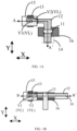
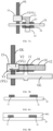
- FIG. 1A is a plan view of a thin film transistor provided in some embodiments of the present disclosure.
- FIG. 1B is a plan view of a thin film transistor provided in further embodiments of the present disclosure.
- FIG. 2A is a cross-sectional view taken along a line A-A' of FIG. 1A .
- FIG. 2B is another cross-sectional view taken along a line A-A' of FIG. 1A .
- FIG. 2C is a cross-sectional view taken along a line B-B' of FIG. 1B .
- FIG. 2D is another cross-sectional view taken along a line B-B' of FIG. 1B .
- FIG. 2E is another cross-sectional view taken along a line B-B' of FIG. 1B .
- FIG. 2F is a further cross-sectional view taken along a line B-B' of FIG. 1B .
- a thin film transistor 10 includes: a gate electrode 11, an active layer 12, a source electrode 13 and a drain electrode 14 on the substrate 20, wherein the active layer 12 is arranged on a side of the source electrode 13 away from the substrate 20, the gate electrode 11 is arranged on a side of the active layer 12 away from the substrate 20, and the source electrode 13 and the drain electrode 14 are connected to the active layer 12.
- the orthographic projection of the first via V1 on the substrate 20 overlaps with the orthographic projection of the hollowed-out portion VL of the gate insulating layer GI on the substrate 20, so that an area occupied by the hollowed-out portion VL and the first via V1 as a whole can be reduced, which is favorable for improving the resolution, reducing a frame width, increasing the light transmittance, and the like.
- the first via V1 extends through the gate insulating layer GI, the active layer 12, and the buffer layer BFL.
- the hollowed-out portion is the second via V2 extending through the gate insulating layer GI.
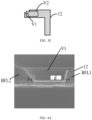
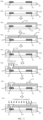
- FIG. 3A is a schematic diagram of positions of a first via, a second via, and an active layer provided in some embodiments of the present disclosure.
- FIG. 3B is a schematic diagram of positions of a first via, a second via, and an active layer provided in further embodiments of the present disclosure.
- FIG. 3C is a schematic diagram of positions of a first via, a second via, and an active layer provided in further embodiments of the present disclosure.
- FIG. 3A is a schematic diagram of positions of a first via, a second via, and an active layer provided in some embodiments of the present disclosure.
- FIG. 3B is a schematic diagram of positions of a first via, a second via, and an active layer provided in further embodiments of the present disclosure.
- FIG. 3C is a
- FIG. 3D is a schematic diagram of positions of a first via, a second via, and an active layer provided in further embodiments of the present disclosure.
- FIG. 3E is a schematic diagram of positions of a first via, a second via, and an active layer provided in further embodiments of the present disclosure.
- the orthographic projection of the first via V1 on the substrate 20 is a first projection
- the orthographic projection of the second via V2 on the substrate 20 is a second projection
- the first projection and the second projection overlap with each other.
- the first projection is located within the second projection.
- the first projection may be located within an orthographic projection of the active layer 12 on the substrate 20 and be spaced apart from a boundary of the orthographic projection of the active layer 12 on the substrate 10.
- the first projection may be located at a corner of the orthographic projection of the active layer 12 on the substrate 20.
- Shapes of the first via V1 and the second via V2 are not particularly limited in the embodiments of the present disclosure.
- the orthographic projection of the first via V1 on the substrate 20 may be circular, rectangular, semicircular, or other irregular shape.
- the orthographic projection of the first via V1 on the substrate 20 may be within the orthographic projection of the active layer 12 on the substrate 20, or beyond the orthographic projection of the active layer 12 on the substrate 20.
- the adapter electrode 15 is connected to the first conductive portion 121 of the active layer 12 through the second via V2, and is connected to the source electrode 13 through the first via V1.
- the second via V2 is formed by directly patterning the gate insulating layer GI, the active layer 12 below the second via V2 may be dry-etched very likely in the etching process due to a small thickness of the active layer 12, which may damage the active layer 12 and further damage the buffer layer BFL below the active layer 12.
- the first via V1/the second via V2 may extend to the light-shielding member 16, and after the adapter electrode 15 is formed in the via, a short circuit may occur between the adapter electrode 15/the source electrode 13 and the light-shielding member 16.
- the light-shielding member 16 is located away from the second via V2 as much as possible.
- the light-shielding member 16 and the second via V2 are staggered, that is, the orthographic projection of the light-shielding member 16 on the substrate 20 does not overlap with the orthographic projection of the second via V2 on the substrate 20.
- the adapter electrode 15 when the adapter electrode 15 is provided in the second via V2, the adapter electrode 15 does not overlap with the light-shielding member 16 in a direction perpendicular to the substrate.
- the gate insulating layer GI is patterned by using a halftone mask process to form the second via V2, so as to avoid damage to the active layer 12. Therefore, in the thin film transistor shown in FIG. 1A , the light-shielding member and the second via are staggered, and the second via is formed by adopting the halftone mask process, so that poor products are avoided.
- the orthographic projection of the light-shielding member 16 on the substrate 20 partially overlaps with the orthographic projection of the second via V2 on the substrate 20.
- the orthographic projection of the light-shielding member 16 on the substrate 20 partially overlaps with the orthographic projection of the adapter electrode 15 on the substrate 20.
- the second via is formed by using the halftone mask process (the specific manufacturing method is described in the following embodiments and is not described here) in the thin film transistor in the embodiment of the present disclosure, so that the active layer 12 may not be damaged, and therefore the buffer layer BLF on a side of the active layer 12 close to the substrate 20 may not be damaged even if the thickness of the active layer 12 is small.
- the orthographic projection of the light-shielding member 16 on the substrate 20 partially overlaps with the orthographic projection of the second via V2 on the substrate 20 only in the thickness direction of the substrate 20, as shown in FIG.
- the light-shielding member 16 and the second via V2 are separated from each other by the active layer 12 and the buffer layer BFL therebetween, and the adapter electrode 15 formed in the second via V2 and the light-shielding member 16 are insulated and separated from each other, so that the short-circuit phenomenon can be avoided.
- connection between the adapter electrode 15 in the first via V1 and the source electrode 13 may be flexibly set.
- the adapter electrode 15 and the source electrode 13 may be electrically connected to each other in a full-coverage manner (that is, the adapter electrode 15 fully covers the source electrode 13).
- the adapter electrode 15 and the source electrode 13 may be electrically connected to each other in a partial lap joint manner (that is, the adapter electrode 15 partially covers the source electrode 13), which is not limited in the embodiment of the present disclosure.
- the adapter electrode 15 may be formed only in a partial region of the second via V2, or may completely fill the second via V2. As shown in FIG. 2A , the orthographic projection of the adapter electrode 15 on the substrate 20 partially overlaps with the orthographic projection of the second via V2 on the substrate 20. Preferably, as shown in FIGS. 2C to 2F , the orthographic projection of the adapter electrode 15 on the substrate 20 covers the orthographic projection of the second via V2 on the substrate 20.
- the light-shielding member 16 and the source electrode 13 are disposed in the same layer.
- the light-shielding member 16 and the source electrode 13 may each employ a Mo/Al/Al metal laminated structure, a MoNb/Cu metal laminated structure, an MTD/Cu metal laminated structure, or a MoNb/Cu/MTD metal laminated structure. Thicknesses of the light-shielding member 16 and the source electrode 13 may be in a range from 1000 ⁇ to 10000 ⁇ .
- the light-shielding member 16 and the source electrode 13 are arranged along the first direction X, and a distance d1 between the light-shielding member 16 and the source electrode 13 in the first direction X is in a range from 1 ⁇ m to 3 ⁇ m, such as 1 ⁇ m, 1.5 ⁇ m, 2 ⁇ m, 2.5 ⁇ m, 3 ⁇ m, or the like, which is not limited in the embodiments of the present disclosure.
- the light-shielding member 16 and the adapter electrode 15 are staggered, and the adapter electrode 15 extends through the first conductive portion 121 of the active layer 12, and the light-shielding member 16 and the channel portion 120 of the active layer are opposite to each other, that is, the first conductive portion 121 and the channel portion 120 of the active layer are also staggered, so that the active layer pattern in FIG. 1A is L-shaped.
- a first active wire is formed between a portion of the active layer 12 connected to the source electrode 13 through the adapter electrode 15 and the channel portion 120
- a second active wire is formed between a portion (i.e., the second conductive portion 122) of the active layer 12 serving as the drain electrode 14 and the channel portion 120, so that the source electrode 13 and the drain electrode 14 are electrically connected to each other when a carrier path is formed in the channel portion 120 of the active layer 12.
- the source electrode 13 of the thin film transistor is connected to a corresponding data line
- the adapter electrode 15 is connected to the source electrode 13 through the second via V2/the first via V1
- the second via V2 does not overlap with the light-shielding member 16 in the direction perpendicular to the substrate 20
- the light-shielding member 16 is directly opposite to the channel portion 120 in the active layer 12, so that the first active wire connecting the source electrode 13 and the channel portion 120 is L-shaped.
- the first active conductive wire is also electrically connected to the data line. If the first active conductive line is too long, the load loss on the data line is increased.
- the channel portion 120 and the second conductive portion 122 of the active layer are arranged along the first direction X, and the first conductive portion 121 is strip-shaped and extends along the first direction X.
- an orthographic projection of a portion of the first conductive portion 121 in contact with the adapter electrode 15 on the substrate 20 and an orthographic projection of the channel portion 120 on the substrate 20 have a distance d3 in a range from 1 ⁇ m and 4 ⁇ m in the first direction X, that is, a length of the first active wire is in a range from 1 ⁇ m to 4 ⁇ m, such as 1 ⁇ m, 1.5 ⁇ m, 2 ⁇ m, 2.5 ⁇ m, 3 ⁇ m, 3.5 ⁇ m, 4 ⁇ m, or the like, which is not limited in the embodiments of the present disclosure.
- the light-shielding member 16 and the source electrode 13 are arranged along the first direction X, and a distance between the light-shielding member 16 and the source electrode 13 is reduced, and correspondingly, the first conductive portion 121 and the channel portion 120 in the active layer 12 are also arranged along the first direction X, and the first conductive portion 121 is strip-shaped. Furthermore, the length of the first active wire is less than or equal to 4 ⁇ m, which is favorable for reducing the load loss on the data line and the area occupied by the whole thin film transistor, thereby improving the resolution.
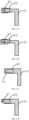
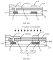
- FIG. 4A is a scanning electron microscope (SEM) image of a longitudinal cross-section of a first via provided in some embodiments of the present disclosure.
- FIG. 4B is a scanning electron microscope (SEM) image of a longitudinal cross-section of a first via and its periphery provided in some embodiments of the present disclosure.
- the orthographic projection of the first via V1 on the substrate 20 is located outside the orthographic projection of the active layer 12 on the substrate 20, as shown in FIG.
- the buffer layer BFL includes a first portion BFL1 covered by the active layer 12 and a second portion BFL2 not in contact with the active layer 12, the first portion has a first slope surface close to the first via V1 and having a slope angle ⁇ in a range from 70° to 90°, and the second portion BFL2 has a second slope surface close to the first via V1 and having a slope angle ⁇ less than or equal to 60°.
- the first via V1 is etched, an upper portion of the second portion BFL2 is covered by a photoresist, and an upper portion of the first portion BFL1 is covered by the active layer 12, so that a topography of the finally formed first via V1 may have the different slope angles.
- An aperture d of the first via V1 at an end of the first via V1 close to the substrate 20 is smaller than 2 ⁇ m.
- the aperture d is in a range from 1.6 ⁇ m to 1.8 ⁇ m.
- the aperture d is 1.65 ⁇ m.
- the buffer layer BFL is formed with a protrusion portion R covering a portion of the source electrode close to the channel portion of the active layer 12.
- a thickness of the protrusion portion R in the direction perpendicular to the substrate is in a range from 1000 ⁇ m to 20000 ⁇ m.
- a surface of the protrusion portion R away from the substrate is an arc surface having a radian in a range from 15° to 90°.
- a portion of the adapter electrode 15 located within the first via V1 is a third portion 15a, a surface of the third portion 15a away from the substrate is a convex surface protruding away from the substrate.
- a portion of the third portion 15a close to an edge of the first via is relatively thin, and a portion of the third portion 15a close to a center of the first via is relatively thick.
- a difference between the maximum thickness and the minimum thickness of the third portion 15a in the direction perpendicular to the substrate is in a range from 0.3 ⁇ m to 0.6 ⁇ m, preferably in a range from 0.35 ⁇ m to 0.55 ⁇ m.
- the hollowed-out portion is the second via V2 extending through the gate insulating layer GI, a difference between a slope angle of a slope surface of the gate insulating layer GI close to the second via V2 and a slope angle of a slope surface of the active layer 12 close to the first via V1 is greater than or equal to 0° and less than or equal to 30°, the slope surface of the gate insulating layer GI and the slope surface of the active layer 12 are on the same side.
- the difference is in a range from 2° to 10°.
- the slope angle of the slope surface of the gate insulating layer GI close to the second via V2 is in a range from 30° to 90°.
- the slope angle of the slope surface of the active layer 12 close to the first via V1 on the same side as the slope surface of the gate insulating layer GI is in a range from 30° to 90°.
- Embodiments of the present disclosure further provide a display substrate.
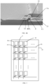
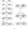
- FIG. 5 is a plan view of a display substrate provided in some embodiments of the present disclosure.
- FIG. 6A is a cross-sectional view of a display substrate provided in some embodiments of the present disclosure.
- FIG. 6B is a cross-sectional view of a display substrate provided in further embodiments of the present disclosure.
- FIG. 7A is a schematic diagram of a connection of a thin film transistor, a gate line and a data line provided in some embodiments of the present disclosure.
- FIG. 7B is a schematic diagram of a connection of a thin film transistor, a gate line and a data line provided in some embodiments of the present disclosure.
- the display substrate includes the thin film transistor 10 in the embodiments described above.
- the display substrate may be used in a liquid crystal display panel, and include: a plurality of gate lines GL extending in the first direction X and a plurality of data lines DL extending in a second direction Y on the substrate 20, which intersect with each other to define a plurality of pixel regions P, each pixel region is provided with the thin film transistor 10 in the above embodiments.
- the gate electrode 11 of the thin film transistor 10 is connected to the corresponding gate line GL
- the source electrode 13 is connected to the corresponding data line DL
- the drain electrode 14 is connected to the pixel electrode 30 in the pixel region P where the thin film transistor 10 is located.
- the gate electrode 11 of the thin film transistor 10 and the corresponding gate line GL have a one-piece structure, and extend along the same direction, and the source electrode 13 of the thin film transistor 10 and the corresponding data line DL have a one-piece structure.
- the gate electrode 11 of the thin film transistor 10 and the corresponding gate line GL have a one-piece structure, and the gate line GL extends along the first direction X, and the gate electrode 11 is a strip-shaped electrode extending along the second direction Y, and the orthographic projection of the light-shielding member 16 on the substrate 20 does not overlap with the orthographic projection of the corresponding gate line GL on the substrate 20.
- the light-shielding member 16 and the source electrode 13 are disposed along the first direction X with a reduced distance therebetween, and correspondingly, the gate electrode 11 and the adapter electrode 15 are disposed along the first direction X with a reduced distance therebetween.
- the reduction of the length of the active layer 12 is favorable for reducing the load loss of the data line.
- the area occupied by the whole thin film transistor on the display substrate is reduced, which is favorable for improving the resolution, reducing the frame width, increasing the light transmittance, and the like.
- a passivation layer PVX and a planarization layer PLN are further disposed on a side of the gate electrode 11 of the thin film transistor 10 away from the substrate 20, the planarization layer PLN is disposed on a side of the passivation layer PVX away from the substrate 20, the passivation layer PVX may be made of one or more of silicon oxide, silicon nitride, and silicon oxynitride, and may have a thickness in a range from 200 nm and 400 nm.
- the planarization layer PLN may have a thickness in a range from 2 ⁇ m to 3 ⁇ m, and be made of the organic material.
- the pixel electrode 30 is located on a side of the planarization layer PLN away from the substrate 20 and is connected to the drain electrode 14 through a third via V3 extending through at least the planarization layer PLN and the passivation layer PVX.
- the pixel electrode 30 may be made of transparent conductive material such as IGZO or IZO, and may have a thickness in a range from 400 ⁇ to 1000 ⁇ .
- the display substrate further includes: an insulating spacer layer (not shown) and a common electrode (not shown), wherein the insulating spacer layer is located on a side of the pixel electrode 30 away from the substrate 20, may be made of at least one of silicon nitride, silicon oxide and silicon oxynitride, and may have a thickness in a range from 1000 ⁇ to 3000 ⁇ .
- the common electrode is located on a side of the insulating spacer layer away from the substrate 20, may be made of a transparent conductive material such as ITO, IZO, or the like, and may have a thickness of 40nm or 135 nm.
- the embodiment of the present disclosure further provides a display apparatus, which includes the display substrate in the above embodiments.
- the display apparatus may be a product or a component with a display function, such as a mobile phone, a tablet computer, a navigator, electronic paper, an OLED panel or the like.
- the step S11 includes forming a source electrode, a buffer layer, an active layer, a drain electrode and a gate insulating layer on a substrate, respectively.
- the source electrode and the drain electrode are electrically connected to the active layer.
Landscapes
- Thin Film Transistor (AREA)
- Liquid Crystal (AREA)
- Devices For Indicating Variable Information By Combining Individual Elements (AREA)
- Electrodes Of Semiconductors (AREA)
Applications Claiming Priority (2)
| Application Number | Priority Date | Filing Date | Title |
|---|---|---|---|
| CN202211353473.0A CN117954495A (zh) | 2022-10-31 | 2022-10-31 | 薄膜晶体管及其制作方法、显示基板和显示装置 |
| PCT/CN2023/091627 WO2024093171A1 (zh) | 2022-10-31 | 2023-04-28 | 薄膜晶体管及其制作方法、显示基板和显示装置 |
Publications (2)
| Publication Number | Publication Date |
|---|---|
| EP4517835A1 true EP4517835A1 (de) | 2025-03-05 |
| EP4517835A4 EP4517835A4 (de) | 2025-10-01 |
Family
ID=90796851
Family Applications (1)
| Application Number | Title | Priority Date | Filing Date |
|---|---|---|---|
| EP23884113.4A Pending EP4517835A4 (de) | 2022-10-31 | 2023-04-28 | Dünnschichttransistor und herstellungsverfahren dafür, anzeigesubstrat und anzeigevorrichtung |
Country Status (6)
| Country | Link |
|---|---|
| US (1) | US20250185289A1 (de) |
| EP (1) | EP4517835A4 (de) |
| JP (1) | JP2025535218A (de) |
| KR (1) | KR20250105294A (de) |
| CN (2) | CN117954495A (de) |
| WO (1) | WO2024093171A1 (de) |
Families Citing this family (1)
| Publication number | Priority date | Publication date | Assignee | Title |
|---|---|---|---|---|
| WO2026025312A1 (zh) * | 2024-07-30 | 2026-02-05 | 京东方科技集团股份有限公司 | 显示基板及其制备方法 |
Family Cites Families (10)
| Publication number | Priority date | Publication date | Assignee | Title |
|---|---|---|---|---|
| US20170090229A1 (en) * | 2014-06-06 | 2017-03-30 | Sharp Kabushiki Kaisha | Semiconductor device, display device and method for manufacturing semiconductor device |
| JP6417125B2 (ja) * | 2014-06-25 | 2018-10-31 | 株式会社ジャパンディスプレイ | 半導体装置 |
| JP2020027133A (ja) * | 2018-08-09 | 2020-02-20 | 株式会社ジャパンディスプレイ | 表示装置 |
| KR102689232B1 (ko) * | 2018-09-20 | 2024-07-29 | 삼성디스플레이 주식회사 | 트랜지스터 기판, 이의 제조 방법, 및 이를 포함하는 표시 장치 |
| CN109742158A (zh) * | 2019-01-31 | 2019-05-10 | 京东方科技集团股份有限公司 | 低温多晶硅薄膜晶体管、阵列基板及制备方法、显示装置 |
| JP7372832B2 (ja) * | 2019-12-26 | 2023-11-01 | シャープ株式会社 | 液晶表示装置およびその製造方法 |
| CN113257835B (zh) * | 2020-02-07 | 2024-11-26 | 夏普株式会社 | 有源矩阵基板及其制造方法 |
| CN111769123B (zh) * | 2020-07-10 | 2023-11-28 | 京东方科技集团股份有限公司 | 一种阵列基板、显示装置和制作方法 |
| CN111897168A (zh) * | 2020-08-21 | 2020-11-06 | 京东方科技集团股份有限公司 | 阵列基板及其制备方法、显示装置 |
| CN113889526B (zh) * | 2021-09-30 | 2024-04-26 | 合肥鑫晟光电科技有限公司 | 薄膜晶体管、显示基板及显示基板的制备方法 |
-
2022
- 2022-10-31 CN CN202211353473.0A patent/CN117954495A/zh active Pending
-
2023
- 2023-04-28 WO PCT/CN2023/091627 patent/WO2024093171A1/zh not_active Ceased
- 2023-04-28 US US18/842,604 patent/US20250185289A1/en active Pending
- 2023-04-28 EP EP23884113.4A patent/EP4517835A4/de active Pending
- 2023-04-28 CN CN202380008916.9A patent/CN118284985A/zh active Pending
- 2023-04-28 KR KR1020247039516A patent/KR20250105294A/ko active Pending
- 2023-04-28 JP JP2024570276A patent/JP2025535218A/ja active Pending
Also Published As
| Publication number | Publication date |
|---|---|
| JP2025535218A (ja) | 2025-10-24 |
| CN118284985A (zh) | 2024-07-02 |
| CN117954495A (zh) | 2024-04-30 |
| US20250185289A1 (en) | 2025-06-05 |
| KR20250105294A (ko) | 2025-07-08 |
| EP4517835A4 (de) | 2025-10-01 |
| WO2024093171A1 (zh) | 2024-05-10 |
Similar Documents
| Publication | Publication Date | Title |
|---|---|---|
| US12310199B2 (en) | Display substrate and display apparatus | |
| US7608493B2 (en) | Thin-film transistor substrate and method of manufacturing the same | |
| KR101246789B1 (ko) | 어레이 기판 및 이의 제조방법 | |
| WO2002089177A2 (en) | A contact structure of a wiring line and method manufacturing the same, and thin film transistor array substrate including the contact structure and method manufacturing the same | |
| CN109004032B (zh) | 薄膜晶体管及其制造方法、阵列基板 | |
| WO2023272503A1 (zh) | 薄膜晶体管及其制备方法、显示基板、显示装置 | |
| KR20110067765A (ko) | 박막 트랜지스터 표시판 및 그 제조 방법 | |
| US20230317826A1 (en) | Method for manufacturing thin film transistor, and thin film transistor | |
| US6998640B2 (en) | Thin film transistor structure | |
| KR20030016051A (ko) | 액정 표시 장치용 박막 트랜지스터 기판 및 그 제조 방법 | |
| CN106997892B (zh) | 显示装置以及该显示装置的制造方法 | |
| EP4517835A1 (de) | Dünnschichttransistor und herstellungsverfahren dafür, anzeigesubstrat und anzeigevorrichtung | |
| KR100783702B1 (ko) | 박막 트랜지스터 기판 및 그 제조 방법 | |
| US7196748B2 (en) | In-plane switching mode liquid crystal display device and method for manufacturing the same | |
| CN215644387U (zh) | 薄膜晶体管 | |
| US8125585B2 (en) | Liquid crystal display device and fabricating method thereof | |
| KR20010096804A (ko) | 배선의 접촉 구조 및 그의 제조 방법과 이를 포함하는박막 트랜지스터 기판 및 그 제조 방법 | |
| US12581731B2 (en) | Array substrate, method for manufacturing the array substrate and display panel | |
| KR20070000247A (ko) | 박막 트랜지스터 기판 및 그 제조 방법 | |
| KR20060136217A (ko) | 박막 트랜지스터 기판 및 그 제조 방법 | |
| KR20040046384A (ko) | 액정표시장치 및 그 제조방법 | |
| KR100709707B1 (ko) | 박막 트랜지스터 기판 및 그 제조 방법 | |
| JP2002091340A (ja) | マトリクスアレイ基板 | |
| CN118507493A (zh) | 显示面板及显示终端 | |
| CN115939151A (zh) | 金属氧化物薄膜晶体管阵列基板及其制作方法和显示面板 |
Legal Events
| Date | Code | Title | Description |
|---|---|---|---|
| STAA | Information on the status of an ep patent application or granted ep patent |
Free format text: STATUS: THE INTERNATIONAL PUBLICATION HAS BEEN MADE |
|
| PUAI | Public reference made under article 153(3) epc to a published international application that has entered the european phase |
Free format text: ORIGINAL CODE: 0009012 |
|
| STAA | Information on the status of an ep patent application or granted ep patent |
Free format text: STATUS: REQUEST FOR EXAMINATION WAS MADE |
|
| 17P | Request for examination filed |
Effective date: 20241126 |
|
| AK | Designated contracting states |
Kind code of ref document: A1 Designated state(s): AL AT BE BG CH CY CZ DE DK EE ES FI FR GB GR HR HU IE IS IT LI LT LU LV MC ME MK MT NL NO PL PT RO RS SE SI SK SM TR |
|
| REG | Reference to a national code |
Ref country code: DE Ref legal event code: R079 Free format text: PREVIOUS MAIN CLASS: H01L0029786000 Ipc: H10D0030670000 |
|
| A4 | Supplementary search report drawn up and despatched |
Effective date: 20250903 |
|
| RIC1 | Information provided on ipc code assigned before grant |
Ipc: H10D 30/67 20250101AFI20250828BHEP Ipc: H10D 86/40 20250101ALI20250828BHEP |
|
| DAV | Request for validation of the european patent (deleted) | ||
| DAX | Request for extension of the european patent (deleted) |