EP4465299A1 - Speichervorrichtung vom phasenwechseltyp und verfahren zum lesen einer solchen vorrichtung - Google Patents
Speichervorrichtung vom phasenwechseltyp und verfahren zum lesen einer solchen vorrichtung Download PDFInfo
- Publication number
- EP4465299A1 EP4465299A1 EP24174247.7A EP24174247A EP4465299A1 EP 4465299 A1 EP4465299 A1 EP 4465299A1 EP 24174247 A EP24174247 A EP 24174247A EP 4465299 A1 EP4465299 A1 EP 4465299A1
- Authority
- EP
- European Patent Office
- Prior art keywords
- memory cell
- current
- reference memory
- initialized state
- celr
- Prior art date
- Legal status (The legal status is an assumption and is not a legal conclusion. Google has not performed a legal analysis and makes no representation as to the accuracy of the status listed.)
- Pending
Links
Images


Classifications
-
- G—PHYSICS
- G11—INFORMATION STORAGE
- G11C—STATIC STORES
- G11C13/00—Digital stores characterised by the use of storage elements not covered by groups G11C11/00, G11C23/00, or G11C25/00
- G11C13/0002—Digital stores characterised by the use of storage elements not covered by groups G11C11/00, G11C23/00, or G11C25/00 using resistive RAM [RRAM] elements
- G11C13/0021—Auxiliary circuits
- G11C13/004—Reading or sensing circuits or methods
-
- G—PHYSICS
- G11—INFORMATION STORAGE
- G11C—STATIC STORES
- G11C16/00—Erasable programmable read-only memories
- G11C16/02—Erasable programmable read-only memories electrically programmable
- G11C16/06—Auxiliary circuits, e.g. for writing into memory
- G11C16/10—Programming or data input circuits
- G11C16/102—External programming circuits, e.g. EPROM programmers; In-circuit programming or reprogramming; EPROM emulators
- G11C16/105—Circuits or methods for updating contents of nonvolatile memory, especially with 'security' features to ensure reliable replacement, i.e. preventing that old data is lost before new data is reliably written
-
- G—PHYSICS
- G11—INFORMATION STORAGE
- G11C—STATIC STORES
- G11C13/00—Digital stores characterised by the use of storage elements not covered by groups G11C11/00, G11C23/00, or G11C25/00
- G11C13/0002—Digital stores characterised by the use of storage elements not covered by groups G11C11/00, G11C23/00, or G11C25/00 using resistive RAM [RRAM] elements
- G11C13/0004—Digital stores characterised by the use of storage elements not covered by groups G11C11/00, G11C23/00, or G11C25/00 using resistive RAM [RRAM] elements comprising amorphous/crystalline phase transition cells
-
- G—PHYSICS
- G11—INFORMATION STORAGE
- G11C—STATIC STORES
- G11C13/00—Digital stores characterised by the use of storage elements not covered by groups G11C11/00, G11C23/00, or G11C25/00
- G11C13/0002—Digital stores characterised by the use of storage elements not covered by groups G11C11/00, G11C23/00, or G11C25/00 using resistive RAM [RRAM] elements
- G11C13/0021—Auxiliary circuits
- G11C13/0064—Verifying circuits or methods
-
- G—PHYSICS
- G11—INFORMATION STORAGE
- G11C—STATIC STORES
- G11C16/00—Erasable programmable read-only memories
- G11C16/02—Erasable programmable read-only memories electrically programmable
- G11C16/06—Auxiliary circuits, e.g. for writing into memory
- G11C16/10—Programming or data input circuits
- G11C16/12—Programming voltage switching circuits
-
- G—PHYSICS
- G11—INFORMATION STORAGE
- G11C—STATIC STORES
- G11C13/00—Digital stores characterised by the use of storage elements not covered by groups G11C11/00, G11C23/00, or G11C25/00
- G11C13/0002—Digital stores characterised by the use of storage elements not covered by groups G11C11/00, G11C23/00, or G11C25/00 using resistive RAM [RRAM] elements
- G11C13/0021—Auxiliary circuits
- G11C13/004—Reading or sensing circuits or methods
- G11C2013/0045—Read using current through the cell
-
- G—PHYSICS
- G11—INFORMATION STORAGE
- G11C—STATIC STORES
- G11C13/00—Digital stores characterised by the use of storage elements not covered by groups G11C11/00, G11C23/00, or G11C25/00
- G11C13/0002—Digital stores characterised by the use of storage elements not covered by groups G11C11/00, G11C23/00, or G11C25/00 using resistive RAM [RRAM] elements
- G11C13/0021—Auxiliary circuits
- G11C13/004—Reading or sensing circuits or methods
- G11C2013/0054—Read is performed on a reference element, e.g. cell, and the reference sensed value is used to compare the sensed value of the selected cell
Definitions
- the invention relates to non-volatile memories, more precisely phase change memories (or PCM: Phase Change Memory) and more particularly to the reading of such memories.
- PCM Phase Change Memory
- Phase change memories are non-volatile memories that rely on the properties of phase change materials.
- a phase change material has, in fact, the capacity to switch from a weakly resistive state to a resistive state thanks to its heating.
- Phase change memories take advantage of the fact that the electrical resistances of different states of phase change materials are different in order to store data.
- the phase change material has the ability to switch from a resistive state (HRS, High Resistive State) to a weakly resistive state (LRS, Low Resistive State) under the effect of heat and the Joule effect generated by the application of a current between electrodes.
- Switching from a resistive state to a low-resistive state corresponds to a programming or activation operation called “SET”, i.e. an operation of writing a binary data value, for example a logical value 1.
- SET programming or activation operation
- the memory is then in a state called “initialized” (SET).
- Switching from a low-resistive state to a resistive state corresponds to an erasure or deactivation operation called “RESET”, i.e. an operation of writing an opposite binary data value, for example a logic value 0.
- RESET erasure or deactivation operation
- the memory is then in a so-called “RESET” state.
- phase change material is heated between its crystallization and melting temperatures and then slowly cooled to obtain a crystalline phase.
- the current pulse therefore exhibits a slow decrease.
- phase change material amorphous (erasing or RESET operation) it is heated above its melting temperature and then cooled rapidly in order to freeze in the amorphous state at room temperature.
- the current pulse is therefore very short and abrupt.
- reading is done in a so-called single-ended mode by comparing the current drawn by the memory cell with a current source and using very relaxed settings to verify the programming and erasure results.
- Another prior art solution consists in performing a differential mode reading between the memory cell and a complementary memory cell (i.e. storing a logical data opposite to the data stored in the memory cell) so as to obtain fast readings in all PVT (Process, Voltage, Temperature) conditions with large current differences.
- PVT Process, Voltage, Temperature
- phase change memory (PCM) type memory device is provided.
- a read amplifier having a first input coupled to the memory cell and a second input coupled to the reference memory cell and configured to deliver information representative of the logic value of the data as a function of the respective values of the first current and the second current.
- the value of the second current is equal to half the difference between the two reference values.
- the distance between the memory cell and the reference memory cell is between 10 micrometers and 20 micrometers.
- the refreshing means comprise a current generator configured to deliver a current pulse to the reference memory cell so as to place it in its initialized state and means for verifying the initialized state of the reference memory cell including the read amplifier.
- the device comprises at least one group of several memory cells associated with the reference memory cell, respectively coupled to the first input of the reading amplifier via controllable switches, and control means configured to successively select said switches so that the reading means can successively read each memory cell of said at least one group.
- the value of the second current is equal to half the difference between the two reference values.
- the reference memory cell is placed at a distance from the memory cell of between 10 micrometers and 20 micrometers.
- the method further comprises a regular refreshing of the reference memory cell to return it to its initialized state.
- the refreshing comprises delivering a current pulse to the reference memory cell so as to place it in its initialized state and verifying the initialized state of the reference memory cell.
- a reference memory cell is associated with several memory cells and each memory cell is read successively using the reference memory cell.
- a reference memory cell is associated with a group of N memory cells, N being an even number, partitioned into two subgroups of N/2 memory cells, and the reference memory cell is placed between the two subgroups of memory cells.
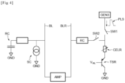
- the DISP reference designates a phase change type memory device comprising here a memory cell phase-change CEL and a phase-change CELR reference memory cell.
- the CEL memory cell and the CELR reference memory cell have an identical structure and are placed side by side.
- phase change memory cell The structure of a phase change memory cell is classical and known per se.
- a memory element for example comprising germanium, antimony and tellurium, which have different resistance values depending on the reset/initialized state (RESET/SET) of the memory.
- This memory element is associated with a heating device, for example two electrodes, which when a current passes through it heats the memory element by Joule effect to vary its resistance.
- the memory cell CEL is associated with a selection transistor TS which is here a PNP bipolar transistor connected in series between the memory element and a cold supply point, typically the GND ground.
- a selection transistor TS which is here a PNP bipolar transistor connected in series between the memory element and a cold supply point, typically the GND ground.
- the base of the bipolar transistor is connected to a word line WL and is intended to receive a voltage turning on this transistor so as to allow current to flow through the heating device so as to heat the memory element.
- bipolar transistors TS and TSR could be replaced by MOS transistors, for example PMOS transistors.
- a CEL memory cell in an initialized state is intended to deliver in reading a first current of the order of 16 microamperes.
- the RC reference designates the parasitic resistances and capacities resulting from the interconnections between the different elements of the DISP device.
- the device DISP also comprises a reading amplifier AMP, of conventional structure and known per se, having a first input E1 and a second input E2 intended to receive two currents when reading the memory cell CEL and to deliver on the output terminal OUT information representative of a data item D having either the logic value 0 or the logic value 1.
- a reading amplifier AMP of conventional structure and known per se, having a first input E1 and a second input E2 intended to receive two currents when reading the memory cell CEL and to deliver on the output terminal OUT information representative of a data item D having either the logic value 0 or the logic value 1.
- MTR treatment methods of the figure 1 here comprise reading means including a first voltage generator GEN1 and a second voltage generator GEN2 intended to be connected respectively to the bit lines BL and BLR.
- bit lines BL and BLR are respectively connected to the two inputs E1 and E2 of the sense amplifier AMP.
- the memory cell CEL is connected to the bit line BL while the reference cell CELR is connected to the bit line BLR.
- the CELR reference cell is placed in its initialized state (SET), for example at the end of the manufacturing of the memory device.
- SET initialized state
- Reading the CEL cell is described with reference to the figure 3 .
- a step ST31 we first apply a voltage VBL1 to the bit line BL and a voltage VBL2 to the bit line BLR.
- VBL1 and VBL2 are respectively delivered by the two current generators GEN1 and GEN2.
- the VBL1 voltage is the one which makes it possible to obtain a current corresponding to the initialized state of the CEL memory cell (typically 16 microamps).
- VBL1 For a bipolar selection transistor, we will choose a voltage VBL1 between 1.5V and 1.8V.
- the voltage VBL2 is a voltage lower than the voltage VBL1, so as to deliver to the reference memory cell CELR a reference current located between a reading current (typically less than or equal to 1 microampere) corresponding to the reset state of the memory cell CEL and a reading current (typically of the order of 16 microamperes) corresponding to the initialized state of the memory cell CEL.
- a reading current typically less than or equal to 1 microampere
- a reading current typically of the order of 16 microamperes
- VBL2 could typically be of the order of 100 to 200 millivolts less than the voltage VBL1.
- memory cell CEL draws a first current Iread which flows in bit line BL while reference memory cell CELR draws a second current Iref which flows in bit line BLR (step ST33).
- the fact that the memory cell CEL and the reference memory cell are placed side by side allows that the voltages applied to the selection transistor bases TS and TSR are substantially the same and that the read paths of the memory cell CEL and the read paths of the reference memory cell CELR are correctly balanced.
- this distance value is only an example and the person skilled in the art will know how to adjust this value, if necessary, depending in particular on the characteristics of the memory cells, the reading patterns and more generally on the application envisaged.
- the reference memory cell may in some cases gradually lose its initialized state.
- the refresh rate depends on the intended application.
- the device further comprises refresh means configured to regularly replace the reference memory cell CELR in its initialized state.
- refresh means here comprise a current generator GEN3 configured to deliver a current pulse PLS (programming pulse) to the reference memory cell CELR so as to place it in its initialized state as well as means for verifying the initialized state of the reference memory cell, these verification means here comprising a current source SC as well as the read amplifier AMP.
- PLS current pulse
- a first switch SW1 for example a MOS transistor, is connected between the generator GEN3 and the reference memory cell CELR.
- a second switch SW2 for example a MOS transistor, is connected between the memory cell CELR and the bit line BLR.
- the RC reference designates the parasitic resistances and capacities of the interconnections.
- switch SW1 is closed and switch SW2 is open.
- generator GEN3 is connected to the reference memory cell CELR and the sense amplifier AMP is not.
- step ST40 the CELR memory cell is programmed so as to place it in its initialized state (SET).
- the PLS pulse is delivered having a classical shape adapted to place a PCM type memory cell in its initialized state.
- switch SW1 is opened and switch SW2 is closed so as to proceed in step ST41 to a verification of the initialized state of the reference memory cell CELR.
- step ST410 we deliver, for example using the generators GEN1 and GEN2 of the figure 2 , or using another single generator, the same voltage VBLV on the bit lines BL and BLR.
- This VBLV voltage is chosen so as to emulate a current of 16 microamperes corresponding to the initialized state of a memory cell.
- the current source SC then draws a current I vsense into the bit line BL while the reference memory cell CELR draws a current Iread into the bit line BLR (step ST412).
- the two currents are compared in the sense amplifier AMP (step ST42).
- the AMP amplifier does not output a logic 1, then it means that the CELR memory cell is not correctly programmed.
- the current source SC can be variable depending on the temperature.
- PTAT proportional to absolute temperature
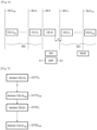
- the memory device comprises a memory plane comprising a matrix of memory cells CEL organized in rows and columns.
- a row of memory cells contains groups of several memory cells.
- the figure 6 illustrates a single group of several memory cells CELG i and CELD i respectively coupled to the first input E1 of the reading amplifier AMP via controllable switches SW.
- This reference memory cell is connected to the second input E2 of the read amplifier as shown above.
- MCM control means for example a logic circuit, are then configured to successively select said switches SW so that the reading means can successively read each memory cell CEL as explained above.
- the reference memory cell CELR is framed by a first subgroup of N/2 memory cells CELG 1 -CELG N/2 and by a second group of N/2 memory cells CELD 1 -CELD N/2 .
- the distance D between each CELG 1 -CELD 1 memory cell immediately adjacent to the reference memory cell is, as indicated above, preferably of the order of 10 to 20 microns.
- step ST7G1 we first read the first cell on the left CELG 1 (step ST7G 1 ) then successively the other cells on the left until we read the cell CELG N/2 (step ST7G N/2 ).
- step ST7D 1 we read the first cell on the right CELD 1 (step ST7D 1 ) then successively the other cells on the right until we read the cell CELD N/2 in step ST7D N/2 .
Landscapes
- Chemical & Material Sciences (AREA)
- Crystallography & Structural Chemistry (AREA)
- Engineering & Computer Science (AREA)
- Computer Security & Cryptography (AREA)
- Dram (AREA)
- Semiconductor Memories (AREA)
- Read Only Memory (AREA)
Applications Claiming Priority (1)
| Application Number | Priority Date | Filing Date | Title |
|---|---|---|---|
| FR2304986A FR3148861A1 (fr) | 2023-05-19 | 2023-05-19 | Dispositif de mémoire du type à changement de phase et procédé de lecture d’un tel dispositif. |
Publications (1)
| Publication Number | Publication Date |
|---|---|
| EP4465299A1 true EP4465299A1 (de) | 2024-11-20 |
Family
ID=88207486
Family Applications (1)
| Application Number | Title | Priority Date | Filing Date |
|---|---|---|---|
| EP24174247.7A Pending EP4465299A1 (de) | 2023-05-19 | 2024-05-06 | Speichervorrichtung vom phasenwechseltyp und verfahren zum lesen einer solchen vorrichtung |
Country Status (4)
| Country | Link |
|---|---|
| US (1) | US20240386955A1 (de) |
| EP (1) | EP4465299A1 (de) |
| CN (1) | CN119007780A (de) |
| FR (1) | FR3148861A1 (de) |
Citations (2)
| Publication number | Priority date | Publication date | Assignee | Title |
|---|---|---|---|---|
| US20080316803A1 (en) * | 2007-06-25 | 2008-12-25 | Industrial Technology Research Institute | Sensing circuit of a phase change memory and sensing method thereof |
| US20140153326A1 (en) * | 2012-12-04 | 2014-06-05 | Macronix International Co., Ltd. | Cell sensing circuit for phase change memory and methods thereof |
Family Cites Families (1)
| Publication number | Priority date | Publication date | Assignee | Title |
|---|---|---|---|---|
| KR101001144B1 (ko) * | 2009-05-12 | 2010-12-17 | 주식회사 하이닉스반도체 | 상변환 메모리 장치 |
-
2023
- 2023-05-19 FR FR2304986A patent/FR3148861A1/fr active Pending
-
2024
- 2024-05-06 EP EP24174247.7A patent/EP4465299A1/de active Pending
- 2024-05-10 US US18/660,938 patent/US20240386955A1/en active Pending
- 2024-05-20 CN CN202410621727.5A patent/CN119007780A/zh active Pending
Patent Citations (2)
| Publication number | Priority date | Publication date | Assignee | Title |
|---|---|---|---|---|
| US20080316803A1 (en) * | 2007-06-25 | 2008-12-25 | Industrial Technology Research Institute | Sensing circuit of a phase change memory and sensing method thereof |
| US20140153326A1 (en) * | 2012-12-04 | 2014-06-05 | Macronix International Co., Ltd. | Cell sensing circuit for phase change memory and methods thereof |
Also Published As
| Publication number | Publication date |
|---|---|
| CN119007780A (zh) | 2024-11-22 |
| US20240386955A1 (en) | 2024-11-21 |
| FR3148861A1 (fr) | 2024-11-22 |
Similar Documents
| Publication | Publication Date | Title |
|---|---|---|
| US6754107B2 (en) | Single supply voltage, nonvolatile phase change memory device with cascoded column selection and simultaneous word read/write operations | |
| US7324371B2 (en) | Method of writing to a phase change memory device | |
| TWI402846B (zh) | 半導體積體電路裝置 | |
| JP5607870B2 (ja) | 電流センス回路及びこれを備えた半導体記憶装置 | |
| EP3092646B1 (de) | Verfahren und schaltung zur programmierung nichtflüchtiger speicherzellen eines flüchtigen/nichtflüchtigen speicherarray | |
| KR100872165B1 (ko) | 저항체를 이용한 비휘발성 메모리 장치 | |
| EP0318363A1 (de) | Verfahren zum Testen von Zellen von elektrisch programmierbaren Speichern und entsprechende integrierte Schaltung | |
| EP2821998B1 (de) | Nichtflüchtige Speichervorrichtung | |
| US20110267877A1 (en) | Semiconductor device | |
| FR2976711A1 (fr) | Cellule memoire avec memorisation volatile et non volatile | |
| FR2970590A1 (fr) | Cellule mémoire volatile/non volatile sans charge | |
| WO2016087763A1 (fr) | Circuit de lecture pour mémoire résistive | |
| KR20090016199A (ko) | 상 변화 메모리 장치 및 그 동작방법 | |
| FR2970589A1 (fr) | Cellule mémoire volatile/non volatile | |
| EP3092647B1 (de) | Speicher mit zugehörigen flüchtigen und nichtflüchtigen speicherzellen | |
| FR2970593A1 (fr) | Cellule mémoire volatile/non volatile compacte | |
| EP1326258B1 (de) | Nichtflüchtiger Phasenänderungsspeicher mit nur einer Speisespannung, Kaskoden-Spaltenauswahl und gleichzeitigen Wortlese- und -schreiboperationen | |
| EP4465299A1 (de) | Speichervorrichtung vom phasenwechseltyp und verfahren zum lesen einer solchen vorrichtung | |
| US8189373B2 (en) | Phase change memory device using a multiple level write voltage | |
| EP4016531B1 (de) | Speicher mit einer matrix aus resistiven speicherzellen und entsprechendes schnittstellenverbindungsverfahren | |
| EP2977988B1 (de) | Nicht-flüchtiger speicher mit programmierbarem widerstand | |
| US20080247216A1 (en) | Method and apparatus for implementing improved write performance for pcram devices | |
| EP4465298A1 (de) | Auslesen einer nichtflüchtigen mehrstufigen speichervorrichtung, insbesondere phasenänderungsspeicher, und nichtflüchtige mehrstufige speichervorrichtung | |
| US20100124101A1 (en) | Phase-change random access memory device | |
| FR2786910A1 (fr) | Memoire a grille flottante multiniveau |
Legal Events
| Date | Code | Title | Description |
|---|---|---|---|
| PUAI | Public reference made under article 153(3) epc to a published international application that has entered the european phase |
Free format text: ORIGINAL CODE: 0009012 |
|
| STAA | Information on the status of an ep patent application or granted ep patent |
Free format text: STATUS: REQUEST FOR EXAMINATION WAS MADE |
|
| 17P | Request for examination filed |
Effective date: 20240506 |
|
| AK | Designated contracting states |
Kind code of ref document: A1 Designated state(s): AL AT BE BG CH CY CZ DE DK EE ES FI FR GB GR HR HU IE IS IT LI LT LU LV MC ME MK MT NL NO PL PT RO RS SE SI SK SM TR |