EP4016531B1 - Speicher mit einer matrix aus resistiven speicherzellen und entsprechendes schnittstellenverbindungsverfahren - Google Patents
Speicher mit einer matrix aus resistiven speicherzellen und entsprechendes schnittstellenverbindungsverfahren Download PDFInfo
- Publication number
- EP4016531B1 EP4016531B1 EP21213966.1A EP21213966A EP4016531B1 EP 4016531 B1 EP4016531 B1 EP 4016531B1 EP 21213966 A EP21213966 A EP 21213966A EP 4016531 B1 EP4016531 B1 EP 4016531B1
- Authority
- EP
- European Patent Office
- Prior art keywords
- memory
- voltage
- conversion capacitor
- conversion
- electrical
- Prior art date
- Legal status (The legal status is an assumption and is not a legal conclusion. Google has not performed a legal analysis and makes no representation as to the accuracy of the status listed.)
- Active
Links
Images


Classifications
-
- H—ELECTRICITY
- H10—SEMICONDUCTOR DEVICES; ELECTRIC SOLID-STATE DEVICES NOT OTHERWISE PROVIDED FOR
- H10B—ELECTRONIC MEMORY DEVICES
- H10B63/00—Resistance change memory devices, e.g. resistive RAM [ReRAM] devices
- H10B63/80—Arrangements comprising multiple bistable or multi-stable switching components of the same type on a plane parallel to the substrate, e.g. cross-point arrays
- H10B63/84—Arrangements comprising multiple bistable or multi-stable switching components of the same type on a plane parallel to the substrate, e.g. cross-point arrays arranged in a direction perpendicular to the substrate, e.g. 3D cell arrays
-
- G—PHYSICS
- G11—INFORMATION STORAGE
- G11C—STATIC STORES
- G11C13/00—Digital stores characterised by the use of storage elements not covered by groups G11C11/00, G11C23/00, or G11C25/00
- G11C13/0002—Digital stores characterised by the use of storage elements not covered by groups G11C11/00, G11C23/00, or G11C25/00 using resistive RAM [RRAM] elements
- G11C13/0004—Digital stores characterised by the use of storage elements not covered by groups G11C11/00, G11C23/00, or G11C25/00 using resistive RAM [RRAM] elements comprising amorphous/crystalline phase transition cells
-
- G—PHYSICS
- G11—INFORMATION STORAGE
- G11C—STATIC STORES
- G11C13/00—Digital stores characterised by the use of storage elements not covered by groups G11C11/00, G11C23/00, or G11C25/00
- G11C13/0002—Digital stores characterised by the use of storage elements not covered by groups G11C11/00, G11C23/00, or G11C25/00 using resistive RAM [RRAM] elements
- G11C13/0021—Auxiliary circuits
- G11C13/003—Cell access
-
- G—PHYSICS
- G11—INFORMATION STORAGE
- G11C—STATIC STORES
- G11C13/00—Digital stores characterised by the use of storage elements not covered by groups G11C11/00, G11C23/00, or G11C25/00
- G11C13/0002—Digital stores characterised by the use of storage elements not covered by groups G11C11/00, G11C23/00, or G11C25/00 using resistive RAM [RRAM] elements
- G11C13/0021—Auxiliary circuits
- G11C13/004—Reading or sensing circuits or methods
-
- G—PHYSICS
- G11—INFORMATION STORAGE
- G11C—STATIC STORES
- G11C13/00—Digital stores characterised by the use of storage elements not covered by groups G11C11/00, G11C23/00, or G11C25/00
- G11C13/0002—Digital stores characterised by the use of storage elements not covered by groups G11C11/00, G11C23/00, or G11C25/00 using resistive RAM [RRAM] elements
- G11C13/0021—Auxiliary circuits
- G11C13/0061—Timing circuits or methods
-
- H—ELECTRICITY
- H10—SEMICONDUCTOR DEVICES; ELECTRIC SOLID-STATE DEVICES NOT OTHERWISE PROVIDED FOR
- H10N—ELECTRIC SOLID-STATE DEVICES NOT OTHERWISE PROVIDED FOR
- H10N70/00—Solid-state devices having no potential barriers, and specially adapted for rectifying, amplifying, oscillating or switching
- H10N70/801—Constructional details of multistable switching devices
- H10N70/821—Device geometry
-
- G—PHYSICS
- G11—INFORMATION STORAGE
- G11C—STATIC STORES
- G11C13/00—Digital stores characterised by the use of storage elements not covered by groups G11C11/00, G11C23/00, or G11C25/00
- G11C13/0002—Digital stores characterised by the use of storage elements not covered by groups G11C11/00, G11C23/00, or G11C25/00 using resistive RAM [RRAM] elements
- G11C13/0021—Auxiliary circuits
- G11C13/004—Reading or sensing circuits or methods
- G11C2013/0045—Read using current through the cell
-
- G—PHYSICS
- G11—INFORMATION STORAGE
- G11C—STATIC STORES
- G11C2213/00—Indexing scheme relating to G11C13/00 for features not covered by this group
- G11C2213/70—Resistive array aspects
- G11C2213/76—Array using an access device for each cell which being not a transistor and not a diode
Definitions
- the technical field is that of microelectronics, more particularly that of resistive memories.
- the invention relates more particularly to a memory comprising a matrix of resistive cells and an electrical device for interfacing this matrix.
- a memory of this type generally comprises an array of memory cells, sometimes called “memory points", each storing a piece of data, for example a binary piece of data.
- the binary piece of data in question is represented by the resistance level, either high or low, of the memory cell in question.
- the data stored in such a memory cell can also be data that can take more than two different values (for example four different values, the data then grouping two bits), in the case of a "multilevel” memory cell.
- the memory cell has a resistance equal to one of its resistance levels (the number of which is greater than two), a level which is associated with the value stored in the cell.
- filament-type memory cells comprising an active layer in which an electrically conductive filament is either broken or, on the contrary, reformed to vary the resistance level of the memory cell, during write cycles and then resetting of this cell (SET operations, when the filament is reformed, and RESET operations, when the filament is broken again).
- SET operations when the filament is reformed, and RESET operations, when the filament is broken again.
- Such a filament-type memory cell may for example be an OxRam type cell (according to the English acronym for "Oxide Random Access Memory"), or a CB-RAM type cell (according to the English acronym for "Conductive Bridge Random Access Memory”).
- the resistive memory cells in question may also be PCRAM type cells (for "Phase Change Memory”). Random Access Memory”), in which an amorphous-crystalline phase change is accompanied by a change in cell resistance.
- one technique consists of applying a reading voltage V' to the cell in question, and measuring the electric current which, in response, passes through the cell. The current value then provides information on the state, either highly resistive or low resistive, of the memory cell.
- the reading voltage is applied between, on the one hand, the row of the matrix where the cell to be read is located, and, on the other hand, the column of the matrix where this cell is located.
- the memory cells in question are sometimes of the "1S1R” type, i.e. comprising, in series: a “1S” stage, acting as a selector and a “1R” stage corresponding to the memory element itself, in which the data is stored (in the form of the resistance level of this element).
- the resistive memory element is the part of the memory cell where the data is stored (in a non-volatile manner), in the form of the resistive state (high or low) of this element.
- this memory element can be of the filamentary type (OxRAM or CBRAM), or phase change.
- the selector is generally made in a so-called “backend” part of the electronic chip comprising the memory, that is to say in a part of this chip made during a second phase of manufacturing of the chip (the memory elements can also be made during this second phase, the entire matrix being part of the "backend”).
- a “1S1R” structure has the advantage of being able to be manufactured by a backend type technology, with stacking of the memory cell and selector matrices. Furthermore, from an electrical point of view, this structure makes it possible to inject a current density which is generally higher than with a traditional frontend technology based on transistors or diodes. This makes it possible to obtain a higher memory density.
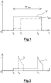
- the reading voltage is then applied in the form of a square-wave pulse, of relatively long duration ⁇ ' lect (longer than the maximum value expected for the incubation time).
- ⁇ ' lect longer than the maximum value expected for the incubation time.
- the instant from which the selector becomes conductive can be located either at the beginning of this pulse (case of instant t' 2 , on the figure 1 ), or rather at the end of it (case of instant t' 1 , on the figure 2 ).
- an electric current i' lect flows through the memory cell for a significant duration (ie: for almost the entire duration of the read pulse). This results in significant electrical consumption, and can also cause a form of alteration or small-scale mechanical stresses (a "stress") within the memory element 1R.
- Phenomena comparable to the incubation phenomenon just presented, for which there is a partly unpredictable delay before a change of conductive or resistive state, can also occur during writing operations (or, in other words, programming) of such a memory cell.
- the document US2013/329484A1 describes a device and a method for carrying out the initialization step of OxRAM type memory cells, this so-called “forming” step consisting of forming the filament for the first time.
- the “forming” step is carried out in a controlled manner, thanks to the use of a “forming” capacitor.
- the conversion capacitor is therefore a reading capacitor, allowing an electrical voltage to be applied to a cell to be read, allowing the cell to be read, while limiting the electrical energy likely to be consumed during this reading.
- the state of the memory cell to be read is determined from the reading voltage in question, present at the terminals of the capacitor after it has been connected to this cell (in practice, after it has discharged, in part, in this cell).
- step b) the conversion capacitor is disconnected from the source, and connected between the row electrical track and the column electrical track in question, by means of the first switch, to perform a conversion between: on the one hand, a resistive state of the memory cell which is located at the intersection of said row electrical track and said column electrical track, and, on the other hand, a charge level of the conversion capacitor.
- charge level we mean the quantity of electrical charges stored in the conversion capacitor, or, equivalently, the electrical voltage at its terminals.
- This arrangement with this conversion capacitor which plays a sort of intermediary role between the electrical source and the matrix, has the advantage of allowing a well-controlled conversion between the two quantities mentioned above (resistive state on the one hand, and charge level on the other), with a natural limitation of energy transfers during this conversion since the energy initially stored in the capacitor is limited (independently of possible latency times in this conversion).
- the conversion capacitor is used here to perform reading operations.
- the conversion in question corresponds to a modification of the charge level of the capacitor, i.e. of the electrical voltage at its terminals, depending on the resistive state of the memory cell read.
- the capacitor is initially charged by the electrical source, which is then disconnected from the capacitor (thanks to the second switch).
- the capacitor is then connected to the matrix (between one of the rows and one of the columns, thanks to the first switch).
- the conversion capacitor will discharge little, and will thus maintain a fairly high voltage. On the contrary, if the memory element is in its low resistive state, the conversion capacitor will discharge into the memory cell, and the voltage across its terminals will drop. The final voltage, across the conversion capacitor, then provides information on the data stored in the memory cell in question.
- the electrical energy consumed during the reading operation is independent of the instant at which the “1S” selector becomes conductive, after the connection of the capacitor (previously charged) to the cell to be read.
- This is illustrated by the figure 2 .
- the moment t o is the instant at which the conversion capacitor, previously charged, is connected to the terminals of the memory cell to be read.
- the selector of this cell becomes conductive, at instant t 1 .
- This is accompanied by a sudden increase in the current i 1 , delivered by the capacitor and which crosses the cell. Then this current decreases, due to the discharge of the capacitor.
- the selector switch occurs earlier, at time t2 , the energy that will be consumed (and dissipated in the memory cell) will remain the same as that consumed during a late switch, since it is limited by the energy initially stored in the capacitor, and by its discharge.
- the electrical energy consumed during such a reading operation is not only independent of the moment of switching of the selector, but it can also be made lower than the energy which would be consumed, on average, with a reading under constant voltage, as will be shown by the exemplary embodiment described below, by way of illustration, with reference to the figure 15 .
- the present invention relates in particular to a memory 1, such as that shown in the figure 3 , which comprises a matrix 2 of resistive memory cells 20 arranged in n rows and m columns.
- the matrix 2 comprises n row electrical tracks L 1 ,...,L i ,...,L n , and m column electrical tracks C 1 ,...,C i ,...,C m , for example metallic.
- the memory cells 20, numbering m ⁇ n, are located at the intersections between the row electrical tracks and the column electrical tracks.
- Each memory cell 20 is connected between, on the one hand, one of the row electrical tracks and, on the other hand, one of the column electrical tracks.
- V for example a reading voltage
- this electrical voltage is applied between, on the one hand, the track L i , and on the other hand the track C j .
- the cell in question, located at the intersection of these two tracks L i and C j is identified by the reference sign 20S, on the figure 3 . From an electrical point of view, everything happens as if a first terminal of this memory cell were connected to track L i , its second terminal being connected to track C j .
- the matrix 2, and more generally the memory 1 can be produced by planar techniques, in the form of a stack of several etched and functionalized layers. As shown in the figure 4 , the column electrical tracks can then be located in a lower layer while the row electrical tracks are located in an upper layer (or vice versa), the cells memories 20 (also called memory points) then extending between this lower layer and this upper layer.
- This type of matrix is often called a "crossbar" type matrix, in this technical field.
- the resistive element 20 In its low resistive state, the resistive element 20 has a low electrical resistance noted R SET RRAM , and in its highly resistive state it has a high electrical resistance noted R RESET RRAM .
- the writing operations in question are sometimes called programming operations, in this technical field.
- Data may be written and stored in each memory cell 20, this data being represented by the resistance level of the memory element 22.
- the data in question is binary data, and the memory cells are programmed so as to place their respective memory elements 22 either in their high resistive state or in their low resistive state.
- multilevel elements more than two distinct resistance levels could be used for each memory element ("multilevel" elements), so as to store in each cell data capable of taking more than two different values.
- the present technology based in particular on a specific conversion capacitor, is presented below in the case of two-level memory elements but it can also be applied to multilevel memory cells as mentioned above.
- the memory cells 20 are of the “1S1R” type, that is to say that they comprise, in addition to the memory element 22, a selector 21 arranged in series with the memory element 22 ( figure 4 ). From an electrical point of view, the selector 21 and the memory element are connected in series, one after the other, between the two corresponding tracks L i , C j .
- the selectors 21 can be produced in a so-called "backend" part of the electronic chip comprising the memory 1.
- the selector 21 may be a selector of the MIEC type, according to the English acronym for “Mixed lonic Electronic Conduction", of the MIT type ("metal-insulator transition switch") or of the OTS type (for "Ovonic Threshold Switch”) which are threshold switches produced from films of amorphous chalcogenide alloys, such an alloy being composed of a non-oxygen chalcogen element (S, Se, Te), in alloy with elements such as Ge, Si, Sb, As, Al, Zn, Ga. They may be doped with light elements such as B, C, N, O, P (with dopant concentrations that may be greater than 1 atomic %).
- the selectors 21 are of the OTS type.
- the selector 21 becomes electrically conductive when the voltage across its terminals becomes greater than a selector threshold voltage.
- V th Sel and which is electrically insulating otherwise.
- electrically conductive we mean that it then has an electrical resistance R ON Sel low, for example less than 30 kiloohms, or even less than 3 kiloohms.
- R ON Sel electrical resistance
- the electrical resistance of the selector is significantly higher, for example by a factor of 10 4 , or 10 5 (and it varies according to the voltage, in general), and the selector is electrically insulating.
- electrically insulating it is meant that it has a high electrical resistance, for example greater than 1 megohm, or even 3 megohms.
- the selector when it is electrically conductive, it may in particular have a resistance lower than the low electrical resistance R SET RRAM of the memory element 22, while when it is electrically insulating, it can exhibit a resistance greater than the high electrical resistance R RESET RRAM of this element.
- the selector 21 is electrically conductive when the voltage at its terminals is greater than the selector threshold voltage. V th Sel , and further provided that the current i flowing through the selector remains greater than a holding current I h .
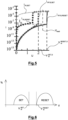
- FIG. 5 shows current-voltage characteristics for the memory element 22 alone, and for the complete memory cell 20 (memory element 22 + selector 21).
- the memory element 22 is of the OxRAM type, here.
- the electric current i flowing through the element considered is represented as a function of the voltage U applied to its terminals (also in arbitrary units).
- the measurement points i 1R,SET and i 1R,RESET correspond to the memory element 22 alone, respectively in its low-resistive state and in its high-resistive state.
- the measurement points i 1R1S,SET and i 1R1S,RESET correspond to the entire memory cell, when the memory element 22 is, respectively, in its low-resistive state and in its high-resistive state.
- the resistance of the memory element, R SET RRAM (e.g. of the order of tens of kilohms) is significantly smaller than that of the selector (the resistance of the selector, just below the selector threshold voltage V th Sel , is typically of the order of a megohm).
- Most of the voltage U applied to the memory cell 20 is therefore found at the terminals of the selector 21 (the voltage U is mainly distributed at the terminals of the selector).
- the low voltage threshold V th SET , o is therefore equal to, or at least close to, the selector threshold voltage V th Sel .
- the memory cell When the voltage U remains below V th RESET , o , the memory cell has a high memory resistance R cell OFF , equal to the sum of the electrical resistance R RESET RRAM of the memory element 22 in its highly resistive state, and of a resistance of the selector 21 in the blocked state (which, under these conditions, can be expressed as U/I th , where I th is the “threshold” current flowing through the selector for a voltage just below the threshold V th Sel ) .
- the various memory cells 20 of the matrix may, from the point of view of their operating characteristics (voltage thresholds, resistance levels, etc.), exhibit a certain disparity with respect to one another, whether immediately after the manufacture and commissioning of the memory, or later, due to different aging between cells. In any event, when controlling the memory 1, it is desirable to take this disparity into account.
- FIG. 6 schematically represents the way in which the low voltage threshold and the high voltage threshold are distributed among the different cells of matrix 2.
- the voltages are represented on the abscissa, while the proportion of cells having a given low or high voltage threshold is represented on the ordinate, corresponding to the voltage value in question.
- the expression “low voltage threshold” also designates the quantity V th SET .
- the expression “high voltage threshold” designates the quantity V th RESET .
- V th SET And V th RESET clearly allows to read any of the memory cells of the matrix without risk of rewriting it (or at least with a low risk of rewriting).
- the memory 1 comprises, in addition to the matrix 2, an interfacing device 3 for interfacing said matrix 2.
- the interfacing device 3 here makes it possible to address a particular memory cell of the matrix, that is to say to connect it electrically (by a system of switches) to an electrical circuit for controlling the cell, in order to interact with it.
- Switches 5 and 6 are, for example, transistors.
- Source 7 is capable of charging conversion capacitor 4. This is a voltage source (made, for example, in the form of a voltage regulator, itself electrically powered). Alternatively, it could be a current source, or any source capable of delivering an arbitrary current and voltage.
- First switch 5 is connected between conversion capacitor 4 and one of the row electrical tracks, or one of the column electrical tracks of the matrix.
- Second switch 6 is connected between the conversion capacitor and source 7.
- This arrangement with this conversion capacitor 4 which plays a sort of intermediary role between the source 7 and the matrix 2, has the advantage of allowing a well-controlled conversion between the two quantities mentioned above (resistive state on the one hand, and charge state on the other), with a natural limitation of the energy transfers during this conversion since the energy initially stored in the capacitor is limited (the capacitor having a limited electrical capacity).
- the interfacing device 3 comprises a control module 10 arranged to control the first and second switches 5, 6, the control module being configured to control these switches so as not to connect the conversion capacitor 4 simultaneously to the source 7 and to said row and column electrical tracks L i , C j , precisely so that the conversion capacitor 4 fully plays its role as intermediary between the source 7, and the cell 20S addressed by the interfacing device 3.
- the control module 10 is implemented for example in the form of an electrical circuit, for example a programmable electrical circuit, which delivers control signals for the switches, according to a predetermined time sequence.
- the control module 10 is for example integrated on the same electronic chip as the matrix, as are the other components of the interface module 3.
- the interfacing device 3 also comprises an additional resistor R add , here.
- This resistor is connected in series with the conversion capacitor 4, between this capacitor and the row electrical track L i (alternatively, it could be connected between the conversion capacitor and the column electrical track C j , for example).
- This additional resistance makes it possible in particular, by the choice of its value, to limit the maximum electric current delivered by the conversion capacitor in the matrix, which makes it possible to control the electrical exchanges even better, when controlling the matrix.
- the additional resistance is in particular greater than the line resistance of the line or column electrical track L i , C j .
- the additional resistance R add is produced here in the form of a dedicated electrical component (made of resistive material). Alternatively, this resistance could however be the internal resistance (effective resistance) of the first switch 5 in its on state.
- a first terminal 11 of the conversion capacitor 4 is connected to the electrical track of column C j , via an electrical ground M.
- the electrical track of column C j is electrically connected to the ground M, and the first terminal 11 of the conversion capacitor is also electrically connected to this electrical ground.
- a second terminal 12 of the conversion capacitor 4 is connected to the electrical line track L i , via the additional resistor R add and the first switch 5.
- the additional resistor R add is electrically connected between, on the one hand, the second terminal 12 of the capacitor, and, on the other hand, an intermediate terminal 13.
- the first switch is electrically connected between this intermediate terminal 13 on the one hand and the electrical line track L i on the other hand.
- a first terminal 14 of the source 7 is connected to the ground M, while a second terminal 15 of this source is connected to the intermediate terminal 13, via the second switch 6 (the second switch 6 is connected between the second terminal 15 of the source on the one hand, and the intermediate terminal 13 on the other hand).
- the interface device 3 also comprises a voltage measuring device 8, connected between the first and second terminals 11, 12 of the conversion capacitor 4. This device is capable of measuring the voltage at the terminals of the conversion capacitor 4, or at least capable of comparing it to a given predetermined threshold. It is connected to the control module 10 and is capable of communicating to it the result of this voltage measurement, or of this comparison.
- the interfacing device 3 can in particular be used, as here, to carry out reading operations on the memory cells of the matrix.
- the reading result voltage, acquired by the voltage measuring device 8 can be measured by the voltage measuring device 8 (which then delivers a value, for example in the form of logical, digital data), or more simply compared to a given threshold (which constitutes a simplified form of measurement), the result then taking the form of a high or low electrical signal, depending on the result of the comparison, for example.
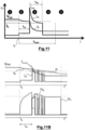
- the selector will not switch to its conductive state, and the conversion capacitor 4 will discharge very little during the reading time t meas , thus maintaining a high voltage.
- the selector will switch to its conductive state, and the conversion capacitor 4 will discharge into the low memory resistor R cell ON , the voltage at its terminals then dropping significantly ( figure 11 ).
- the reading result voltage V R finally measured at the terminals of the conversion capacitor 4, therefore provides information on the data (0 or 1) stored in the memory cell in question.
- FIG 7 represents an equivalent electrical diagram of the memory 1, during a reading operation of the memory cell 20S.
- this figure shows a model representing in a simplified manner the electrical behavior of the memory cell 20S read, and that of the rest of the matrix 2.
- the resistance R line is the electrical resistance of the electrical tracks L i and C j . In practice, it is significantly smaller than R OTS and R RRAM which are, respectively, the resistance of the selector 21 and the resistance of the memory element 22.
- the remainder of the matrix is represented by a matrix leakage resistor, R mat leak , and an overall parasitic capacitance C par tot connected in parallel with the leakage resistor, the assembly being connected between ground M and the first switch 5.
- the overall parasitic capacitance C par tot is representative of an effective electrical capacitance of the part of the matrix 2 which includes the row and the column of memory cells 20 corresponding to the row electrical track L i and to the column electrical track C j , without the memory cell 20S (located at the intersection of this row and this column). It is therefore the effective parasitic capacitance of the (m+n-1) memory cells in question.
- the (m+n-2) cells of row L i and column C j are polarized under a voltage V/2, while the 20S cell is polarized under a voltage V. And as these (m+n-2) cells are polarized, powered, their capacity must be taken into account to determine the electrical response (in particular the response time) of the assembly.
- the overall parasitic capacitance C par tot can be evaluated as (m+n-1) ⁇ C by .
- m+n-1 is the total number of cells (including the 20S cell) that comprise row L i and column C j .
- the expression for C par tot may however be different.
- R mat leak I leak Vleak + 1 Rline + 1 R RESET RRAM ⁇ m + n ⁇ 2 ⁇ 1
- I leak is a leakage current of a cell of the matrix subjected to the voltage V leak (for example V/2).
- the conversion capacitor 4 has been previously charged, to an initial voltage V init , by the source 7. The source is then disconnected (using the second switch 6). Then, at time t o , at the end of a first phase (phase “1”, in the figures), the conversion capacitor 4 is connected to the matrix by closing the first switch 5.
- V eq V init 1 1 + C par tot / C c
- t eq ⁇ ln 1 ⁇ V eq / V init ⁇ R tot OFF .
- C par tot Or R tot OFF is a high total effective resistance into which the conversion capacitor 4 discharges.
- R tot OFF 1 / 1 / R leak mat + 1 / R ′ cell OFF + R add
- R ′ cell OFF is the sum of the high memory resistance R cell Off of the cell and the line resistance R line (the latter being generally negligible, in practice).
- R cell OFF V init I th + R RESET RRAM + R line
- V init / I th is an estimate of the resistance of the selector 21, in its blocked state, under these operating conditions.
- V read RESET V eq ⁇ 1 ⁇ exp ⁇ t meas / ⁇ off
- ⁇ off R tot OFF ⁇ C c + C par tot is the response time of the RC circuit equivalent to memory, in this situation.
- the conversion capacitor 4 is previously charged to the initial voltage V init , as described above, during the first phase (phase “1”, in the figures). At time t o , at the end of the first phase, the conversion capacitor 4 is connected to the matrix by closing the first switch 5.
- the electrical charge initially contained in the conversion capacitor 4 begins to be distributed between this capacitor and the parasitic capacitances during a second phase (phase “2” in the figures), the voltage U SET 20 at the terminals of the memory cell 20S gradually increasing towards the equilibrium voltage V eq . ( figure 10 ).
- t ch ⁇ ln 1 ⁇ V th SET / V init ⁇ R tot OFF .
- the conversion capacitor 4 discharges rapidly into the memory cell 20S, which has the low memory resistance R cell ON . This discharge continues as long as the current i 20 which passes through the cell remains greater than the holding current I h .
- the selector switches back to its blocked state and the current i 20 is significantly reduced, which marks the end of the third phase.
- R tot ON 1 / 1 / R leak mat + 1 / R ′ cell ON + R add
- R ′ cell ON is equal to the sum of the low memory resistance R cell ON of the cell, and the line resistance R line (the latter being generally negligible, in practice):
- the maximum current I max be less than a programming current of the cell, I prog , beyond which there is a risk of modifying the resistive state of the memory element 22, which results in: V init / R tot ON ⁇ I prog
- the additional resistance R add allows, in a particularly convenient way, to adjust the value of the total effective low resistance R tot ON , in order to satisfy condition (F1) above.
- This possibility of adjustment of R tot ON thanks to the additional resistance R add is particularly interesting for an OxRAM type memory, like the one described here, for which the maximum reading current is often quite close to the programming current.
- the maximum current I max be greater than the holding current I h , to effectively switch the selector to its conductive state, i.e. V init / R tot ON > I h
- the discharge current is high (without exceeding I prog ), to discharge the capacitor as much as possible. conversion before the selector is re-blocked. This in fact allows a substantial drop in the voltage across the capacitor, and therefore a greater difference between the reading result voltage for a highly resistive state and for a low resistive state.
- the conversion capacitor It is also desirable to discharge the conversion capacitor to a minimum to avoid an oscillation phenomenon between the conversion capacitor and the memory cell. Indeed, if the conversion capacitor is not sufficiently discharged when the selector re-locks, this capacitor will then charge (by charge distribution) the parasitic capacitances of the memory, thus causing the voltage at the terminals of the cell to return to a value higher than V th SET and thus causing the selector to switch again to its conductive state, which will cause the conversion capacitor to discharge until the selector is re-blocked, and so on until the conversion capacitor is sufficiently discharged, its residual charge no longer allowing it to reach V th SET at the terminals of the memory cell.
- t dis ⁇ ln I h ⁇ R tot ON V th SET ⁇ ⁇ ON
- ⁇ ON R tot ON ⁇ C c + C par tot is the response time of the RC circuit equivalent to memory, in this situation.
- the reading duration t meas is greater than the sum of the duration t meas,min and an expected maximum incubation duration t incub .
- a fourth phase "4" of the reading operation begins when the selector switches back to its blocked state, and ends at the end of the reading duration t meas , when the reading capacitor is disconnected from the matrix (in order to measure the reading result voltage, during a fifth phase "5").
- the reading result voltage V R finally obtained at the end of the fourth phase is therefore equal to, or at least close to, the voltage V read SET at the end of the third phase.
- the capacitance C c of the conversion capacitor is higher, and even significantly higher than the overall parasitic capacitance C par tot . This is also desirable for the overall operation of memory 1.
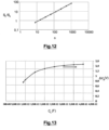
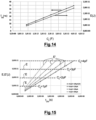
- the figure 13 shows more precisely, for an example, the influence of the capacitance value C c on the width ⁇ V R of the “window” between high and low reading voltages, showing that it is desirable to choose the capacitance C c sufficiently large (compared to C par tot ) to obtain a sufficiently large reading window.
- the capacitance C c choose for example a value between two times and thirty times the overall parasitic capacitance C par tot allows a good compromise to be obtained between these different constraints.
- the additional resistance R add it is preferably chosen so that the total effective resistance low R tot ON either less than V init divided by I h (condition F2 given above), or even less than V th SET / I h (condition F3 given above - which makes it possible to avoid an oscillatory regime), and greater than V init divided I prog (condition F1 - which makes it possible to limit the risks of rewriting when reading).
- the total effective low resistance R tot ON is the total effective resistance into which the conversion capacitor 4 discharges when connected to the memory cell 20S, the cell having its low memory resistance R cell ON (ie: memory element in its low resistive state, and selector in its conductive state).
- the intrinsic duration of the reading operation itself, which is t dis 18 ns, is therefore short (on the other hand, the charging time of the parasitic capacitances, t ch , is rather long, and it would be interesting to reduce it).
- V read RESET 3,8 V
- V read SET 2,5 V
- a reading window ⁇ V R 1.3V.
- the charging time of the parasitic capacitances t ch is much greater than the intrinsic reading time t dis .
- a total reading time of less than 50ns can for example be envisaged by taking the same parameters as above, but by reducing the value of the elementary parasitic capacitance C par at 0.1fF.
- the data from the figure 12 correspond to typical characteristics of a manufacturing process with fine engraving (with a pitch between lines of, for example, between 20 and 40 nanometers).
- the ratio S 2 /S 4 is greater than 1 (for the numerical example given above, it is equal to 10, for example).
- the conversion capacitor thus produced therefore occupies a smaller surface area than that of the matrix.
- the increase in the ratio S 2 /S 4 with the dimension n, visible on the figure 12 can be explained as follows.
- the surface area S2 of the matrix increases as n 2
- the overall parasitic capacitance C par tot and hence the minimum value of the capacitance C c , increase as n (more precisely, proportionally, as 2n-1), so that the ratio S 2 /S 4 finally increases with n.
- the four energy values E are those corresponding to the curve of the figure 14 .
- the energy E' 4 curves are represented, respectively associated with a reading current I read of 100, 120, 150 and 200 microamperes. For each of these curves, the energy E' is represented as a function of an average duration in the on state t ON . This duration corresponds to the average time during which the memory cell (and in particular its selector) is conductive.
- a reading pulse ( figure 1 ) for at least 50ns, which leads to an average duration in the on state t ON of approximately 25ns (this is a very schematic example, but in any case, in practice, t ON is typically between ten and a few tens of ns).
- t ON is typically between ten and a few tens of ns.
- This method can then include a step of determining the data (0 or 1, for example) stored in the memory cell 20S, as a function of the reading result voltage V R .
Landscapes
- Chemical & Material Sciences (AREA)
- Crystallography & Structural Chemistry (AREA)
- Semiconductor Memories (AREA)
Claims (13)
- Speicher (1) bestehend aus:- einer Matrix (2) aus resistiven Speicherzellen (20) mit:o elektrischen Zeilenspuren (L1, Li, Ln),o elektrischen Spaltenspuren (C1, Cj, Cm), undo resistiven Speicherzellen (20), die sich an den Kreuzungen zwischen den elektrischen Zeilenspuren (L1,Li,Ln) und den elektrischen Spaltenspuren (C1,Cj,Cm) befinden, wobei jede Speicherzelle (20) zwischen einerseits einer der elektrischen Zeilenspuren und andererseits einer der elektrischen Spaltenspuren angeschlossen ist,- wobei der Speicher (1) eine Schnittstellenvorrichtung (3) zum Anschließen der Matrix (2) umfasst und die Schnittstellenvorrichtung mindestens einen Wandlerkondensator (4), eine Spannungsmessvorrichtung (8), die mit den Anschlüssen des Wandlerkondensators (4) verbunden ist, eine elektrische Quelle (7), einen ersten Schalter (5), einen zweiten Schalter (6) und ein Steuermodul (10) umfasst, wobei die Schnittstellenvorrichtung (3) so konfiguriert ist, dass sie die folgenden Schritte ausführt:∘ Schritt a): Verbinden des Wandlerkondensators (4) mit der Quelle (7) mittels des zweiten Schalters (6), um den Wandlerkondensator (4) aufzuladen, und danno Schritt b):- Trennen des Wandlerkondensators (4) von der Quelle (7) und Verbinden des Wandlerkondensators (4) zwischen einer der elektrischen Zeilenspuren (Li) und einer der elektrischen Spaltenspuren (Cj) mittels des ersten Schalters (5), und dann- Erfassen einer Spannung nach dem Ergebnis eines Ablesens (VR) an den Anschlüssen (11, 12) des Wandlerkondensators (4) mit Hilfe der Spannungsmessvorrichtung (8), und dann- Bestimmen eines resistiven Zustands der Zelle (20S) durch das Steuermodul (10) auf der Grundlage der Spannung des abgelesenen Ergebnisses (VR).
- Speicher (1) nach dem vorhergehenden Anspruch, bei dem die Schnittstellenvorrichtung (3) einen zusätzlichen Widerstand (Radd) umfasst, der in Reihe mit dem Wandlerkondensator (4) geschaltet ist.
- Speicher (1) nach einem der vorhergehenden Ansprüche, bei dem der Wandlerkondensator (4) eine Kapazität (Cc) aufweist, die größer als eine gesamte parasitäre Kapazität ist (

- Speicher (1) nach einem der vorhergehenden Ansprüche, bei dem das Steuermodul (10) so konfiguriert ist, dass es den ersten und den zweiten Schalter (5, 6) so steuert, dass die Schritte a) und b) ausgeführt werden.
- Speicher (1) nach Anspruch 4, bei dem das Steuermodul (10) zudem so konfiguriert ist, um:- in Schritt a) den zweiten Schalter (6) oder die Quelle (7) so zu steuern, dass der Wandlerkondensator (4) bis zu einer gegebenen Initialisierungsspannung (Vinit) aufgeladen wird,- in Schritt b) den ersten und zweiten Schalter (5, 6) so zu steuern, dass die Quelle (7) von dem Wandlerkondensator (4) getrennt und dann der Wandlerkondensator (4) zwischen der elektrischen Zeilenspur (Li) und der elektrischen Spaltenspur (Cj) für eine vorbestimmte Lesezeit der Speicherzelle (tmeas) verbunden wird, bevor die Spannung des abgelesenen Ergebnisses (VR) erfasst wird.
- Speicher (1) nach einem der vorhergehenden Ansprüche,- in dem jede Speicherzelle (20) ein Speicherelement (22) mit mindestens einem hochohmigen Zustand (RESET) und einem niederohmigen Zustand (SET) sowie einen Selektor (21) umfasst, der in Reihe mit dem Speicherelement (22) angeordnet ist, wobei der Selektor elektrisch leitend ist, wenn eine Spannung an seinen Anschlüssen größer als ein Grenzwert (
 - und in dem, wenn an den Anschlüssen der Speicherzelle (20) eine Spannung (U) angelegt wird, die zwischen einem niedrigen Spannungsgrenzwert (
 o wenn das Speicherelement (22) in seinem niederohmigen Zustand (SET) ist, dann wird der Selektor elektrisch leitend und die Speicherzelle (20) hat dann einen niederohmigen Speicherwiderstand (
 o während, wenn das Speicherelement (22) in seinem hochohmigen Zustand (RESET) ist, dann bleibt der Selektor elektrisch isolierend und die Speicherzelle (20) weist dann einen hohen Speicherwiderstand auf (
- Speicher (1) nach den Ansprüchen 5 und 6, wobei die Initialisierungsspannung (Vinit):- größer ist als der untere Spannungsgrenzwert (
 - kleiner ist als der obere Spannungsgrenzwert (
 - wobei der Koeffizient (α) für den Ausgleich der Ladungsverteilung gleich der Summe aus der Kapazität des Wandlerkondensators (Cc) und einer gesamten parasitären Kapazität (

- Speicher (1) nach Anspruch 7, bei dem die Lesedauer (tmeas) größer ist als: ein oberer effektiver Gesamtwiderstand (


- Speicher (1) nach den Ansprüchen 2, 5 und 6,- bei dem der Selektor (21) elektrisch leitend ist, unter der weiteren Voraussetzung, dass ein elektrischer Strom (i), der durch den Selektor (21) fließt, größer als ein Haltestrom (ih) bleibt,- und in dem der zusätzliche Widerstand (Radd) so beschaffen ist, dass ein niedriger effektiver Gesamtwiderstand (


- Speicher (1) nach Anspruch 9, wobei der zusätzliche Widerstand (Radd) so beschaffen ist, dass der niedrige effektive Gesamtwiderstand (


- Speicher (1) nach einem der vorhergehenden Ansprüche, in dem der Wandlerkondensator (4) auf oder unter der Matrix (2) der Speicherzellen (20) angeordnet ist und sich parallel zur Matrix (2) erstreckt, wobei die Matrix (2) und der Wandlerkondensator (4) einander überlagert sind.
- Verfahren zur Schnittstellenbildung eines Speichers (1) gemäß einem der vorhergehenden Ansprüche, das die folgenden Schritte umfasst:- Schritt a): Verbinden des Wandlerkondensators (4) mit der Quelle (7) mittels des zweiten Schalters (6), um den Wandlerkondensator (4) aufzuladen, und dann- Schritt b):∘ Trennen des Wandlerkondensators (4) von der Quelle (7) und Verbinden des Wandlerkondensators (4) zwischen einer der elektrischen Zeilenspuren (Li) und einer der elektrischen Spaltenspuren (Cj) mittels des ersten Schalters (5), danno Erfassen einer Spannung nach dem Ergebnis eines Ablesens (VR) an den Anschlüssen (11, 12) des Wandlerkondensators (4) mit Hilfe der Spannungsmessvorrichtung (8), und danno Bestimmen eines resistiven Zustands der Zelle (20S) durch das Steuermodul (10) auf der Grundlage der Spannung des abgelesenen Ergebnisses (VR).
- Verfahren nach dem vorhergehenden Anspruch, in dem der Speicher (1) die Spannungsmessvorrichtung (8) umfasst, die mit den Anschlüssen (11, 12) des Wandlerkondensators (4) verbunden ist, wobei:- in Schritt a) der zweite Schalter (6) oder die Quelle (7) so gesteuert werden, dass der Wandlerkondensator (4) bis zu einer gegebenen Initialisierungsspannung (Vinit) aufgeladen wird,- in Schritt b) der erste und zweite Schalter (5, 6) so gesteuert werden, dass die Quelle (7) von dem Wandlerkondensator (4) getrennt und dann der Wandlerkondensator (4) zwischen der elektrischen Zeilenspur (Li) und der elektrischen Spaltenspur (Cj) für eine vorbestimmte Lesezeit der Speicherzelle (tmeas) verbunden wird, bevor die Spannung des abgelesenen Ergebnisses (VR) erfasst wird.
Applications Claiming Priority (1)
| Application Number | Priority Date | Filing Date | Title |
|---|---|---|---|
| FR2013374A FR3117660B1 (fr) | 2020-12-16 | 2020-12-16 | Mémoire comprenant une matrice de cellules mémoires résistives, et procédé d’interfaçage associé |
Publications (2)
| Publication Number | Publication Date |
|---|---|
| EP4016531A1 EP4016531A1 (de) | 2022-06-22 |
| EP4016531B1 true EP4016531B1 (de) | 2025-02-05 |
Family
ID=75438899
Family Applications (1)
| Application Number | Title | Priority Date | Filing Date |
|---|---|---|---|
| EP21213966.1A Active EP4016531B1 (de) | 2020-12-16 | 2021-12-13 | Speicher mit einer matrix aus resistiven speicherzellen und entsprechendes schnittstellenverbindungsverfahren |
Country Status (3)
| Country | Link |
|---|---|
| US (1) | US12052876B2 (de) |
| EP (1) | EP4016531B1 (de) |
| FR (1) | FR3117660B1 (de) |
Families Citing this family (1)
| Publication number | Priority date | Publication date | Assignee | Title |
|---|---|---|---|---|
| US12243614B2 (en) * | 2022-10-17 | 2025-03-04 | Globalfoundries U.S. Inc. | Single ended sense amplifier with current pulse circuit |
Family Cites Families (6)
| Publication number | Priority date | Publication date | Assignee | Title |
|---|---|---|---|---|
| US6954392B2 (en) * | 2003-03-28 | 2005-10-11 | Micron Technology, Inc. | Method for reducing power consumption when sensing a resistive memory |
| JP2013254545A (ja) * | 2012-06-08 | 2013-12-19 | Sharp Corp | 不揮発性半導体記憶装置、及び、可変抵抗素子の抵抗制御方法 |
| KR102155060B1 (ko) * | 2014-10-24 | 2020-09-11 | 에스케이하이닉스 주식회사 | 멀티 레벨 메모리 소자 및 그의 데이터 센싱 방법 |
| KR102352890B1 (ko) * | 2015-05-06 | 2022-01-19 | 삼성전자주식회사 | 플라잉 커패시터 전압 제어를 위한 회로들을 가지는 dc-dc 컨버터 및 그에 따른 전압 제어 방법 |
| US10049713B2 (en) * | 2016-08-24 | 2018-08-14 | Micron Technology, Inc. | Full bias sensing in a memory array |
| US10714185B2 (en) * | 2018-10-24 | 2020-07-14 | Micron Technology, Inc. | Event counters for memory operations |
-
2020
- 2020-12-16 FR FR2013374A patent/FR3117660B1/fr active Active
-
2021
- 2021-12-13 US US17/549,162 patent/US12052876B2/en active Active
- 2021-12-13 EP EP21213966.1A patent/EP4016531B1/de active Active
Also Published As
| Publication number | Publication date |
|---|---|
| US12052876B2 (en) | 2024-07-30 |
| US20220190037A1 (en) | 2022-06-16 |
| FR3117660B1 (fr) | 2023-12-22 |
| FR3117660A1 (fr) | 2022-06-17 |
| EP4016531A1 (de) | 2022-06-22 |
Similar Documents
| Publication | Publication Date | Title |
|---|---|---|
| EP2541770B1 (de) | Verzögerungsgenerator, der einen programmierbaren Widerstand aus Phasenwechselmaterial benutzt | |
| EP1014447A1 (de) | Einmal programmierbare Speicherzelle, mit CMOS-Technologie hergestellte | |
| FR3011117A1 (fr) | Procede et dispositif de commande d'une memoire reram | |
| FR3066308A1 (fr) | Procede de gestion de l'endurance d'une memoire reinscriptible non volatile et dispositif de programmation d'une telle memoire | |
| EP4016531B1 (de) | Speicher mit einer matrix aus resistiven speicherzellen und entsprechendes schnittstellenverbindungsverfahren | |
| EP2996116B1 (de) | Vorrichtung und verfahren zum schreiben von daten in einen resistiven speicher | |
| EP2996115A1 (de) | Vorrichtung und verfahren zum schreiben von daten in einen resistiven speicher | |
| EP1476878B1 (de) | Zerstörungsfreie einmal programmierbare speicherzelle | |
| EP0421839B1 (de) | Speicher mit verbesserter Lesezeit | |
| EP1420416B1 (de) | Dreiphasenspeicherzelle | |
| FR3118267A1 (fr) | Lecture différentielle de mémoire rram à faible consommation | |
| FR3025927A1 (fr) | Programmation de cellules anti-fusibles | |
| EP2977988B1 (de) | Nicht-flüchtiger speicher mit programmierbarem widerstand | |
| EP4198985A1 (de) | Resistiver speicher mit selektor ausgestattet mit schreibkondensator und schreibverfahren dafür | |
| EP1416497A2 (de) | Einmal programmierbare Multibitspeicherzellen | |
| EP1416498B1 (de) | Auf Speicherzellen basierter monotoner Zähler | |
| EP3401914B1 (de) | Verfahren zur steuerung der lebensdauer eines nicht-flüchtigen überschreibbaren speichers, und programmierungsvorrichtung eines solchen speichers | |
| EP0838824B1 (de) | Speicher mit verbesserter Lesezeit | |
| FR2913806A1 (fr) | Utilisation de spinelles lacunaires a clusters tetraedriques d'element de transition du type am4x8 dans une memoire non volatile reinscriptible de donnees electroniques,et materiau correspondant. | |
| WO2021089478A1 (fr) | Dispositif memoire non volatile selecteur et procede de lecture associe | |
| FR3161303A1 (fr) | Mémoire résistive à accès aléatoire avec courant perturbateur réduit dans une architecture à cellule mémoire à ligne de source partagée | |
| EP4345820B1 (de) | Schaltung zum zerstörungsfreien auslesen ferroelektrischer speicher | |
| EP3239983B1 (de) | Einpoliger resistiver speicher | |
| EP4465299A1 (de) | Speichervorrichtung vom phasenwechseltyp und verfahren zum lesen einer solchen vorrichtung | |
| FR2836750A1 (fr) | Cellule memoire a programmation unique non destructrice |
Legal Events
| Date | Code | Title | Description |
|---|---|---|---|
| PUAI | Public reference made under article 153(3) epc to a published international application that has entered the european phase |
Free format text: ORIGINAL CODE: 0009012 |
|
| STAA | Information on the status of an ep patent application or granted ep patent |
Free format text: STATUS: REQUEST FOR EXAMINATION WAS MADE |
|
| 17P | Request for examination filed |
Effective date: 20211213 |
|
| AK | Designated contracting states |
Kind code of ref document: A1 Designated state(s): AL AT BE BG CH CY CZ DE DK EE ES FI FR GB GR HR HU IE IS IT LI LT LU LV MC MK MT NL NO PL PT RO RS SE SI SK SM TR |
|
| RBV | Designated contracting states (corrected) |
Designated state(s): AL AT BE BG CH CY CZ DE DK EE ES FI FR GB GR HR HU IE IS IT LI LT LU LV MC MK MT NL NO PL PT RO RS SE SI SK SM TR |
|
| GRAP | Despatch of communication of intention to grant a patent |
Free format text: ORIGINAL CODE: EPIDOSNIGR1 |
|
| STAA | Information on the status of an ep patent application or granted ep patent |
Free format text: STATUS: GRANT OF PATENT IS INTENDED |
|
| RIC1 | Information provided on ipc code assigned before grant |
Ipc: G11C 13/00 20060101AFI20240708BHEP |
|
| INTG | Intention to grant announced |
Effective date: 20240717 |
|
| RAP3 | Party data changed (applicant data changed or rights of an application transferred) |
Owner name: WEEBIT NANO LTD Owner name: COMMISSARIAT A L'ENERGIE ATOMIQUE ET AUX ENERGIESALTERNATIVES |
|
| GRAS | Grant fee paid |
Free format text: ORIGINAL CODE: EPIDOSNIGR3 |
|
| GRAA | (expected) grant |
Free format text: ORIGINAL CODE: 0009210 |
|
| STAA | Information on the status of an ep patent application or granted ep patent |
Free format text: STATUS: THE PATENT HAS BEEN GRANTED |
|
| AK | Designated contracting states |
Kind code of ref document: B1 Designated state(s): AL AT BE BG CH CY CZ DE DK EE ES FI FR GB GR HR HU IE IS IT LI LT LU LV MC MK MT NL NO PL PT RO RS SE SI SK SM TR |
|
| REG | Reference to a national code |
Ref country code: GB Ref legal event code: FG4D Free format text: NOT ENGLISH |
|
| REG | Reference to a national code |
Ref country code: CH Ref legal event code: EP |
|
| REG | Reference to a national code |
Ref country code: DE Ref legal event code: R096 Ref document number: 602021025747 Country of ref document: DE |
|
| REG | Reference to a national code |
Ref country code: IE Ref legal event code: FG4D Free format text: LANGUAGE OF EP DOCUMENT: FRENCH |
|
| REG | Reference to a national code |
Ref country code: NL Ref legal event code: MP Effective date: 20250205 |
|
| PG25 | Lapsed in a contracting state [announced via postgrant information from national office to epo] |
Ref country code: RS Free format text: LAPSE BECAUSE OF FAILURE TO SUBMIT A TRANSLATION OF THE DESCRIPTION OR TO PAY THE FEE WITHIN THE PRESCRIBED TIME-LIMIT Effective date: 20250505 |
|
| PG25 | Lapsed in a contracting state [announced via postgrant information from national office to epo] |
Ref country code: FI Free format text: LAPSE BECAUSE OF FAILURE TO SUBMIT A TRANSLATION OF THE DESCRIPTION OR TO PAY THE FEE WITHIN THE PRESCRIBED TIME-LIMIT Effective date: 20250205 |
|
| PG25 | Lapsed in a contracting state [announced via postgrant information from national office to epo] |
Ref country code: PL Free format text: LAPSE BECAUSE OF FAILURE TO SUBMIT A TRANSLATION OF THE DESCRIPTION OR TO PAY THE FEE WITHIN THE PRESCRIBED TIME-LIMIT Effective date: 20250205 |
|
| PG25 | Lapsed in a contracting state [announced via postgrant information from national office to epo] |
Ref country code: ES Free format text: LAPSE BECAUSE OF FAILURE TO SUBMIT A TRANSLATION OF THE DESCRIPTION OR TO PAY THE FEE WITHIN THE PRESCRIBED TIME-LIMIT Effective date: 20250205 |
|
| REG | Reference to a national code |
Ref country code: LT Ref legal event code: MG9D |
|
| PG25 | Lapsed in a contracting state [announced via postgrant information from national office to epo] |
Ref country code: IS Free format text: LAPSE BECAUSE OF FAILURE TO SUBMIT A TRANSLATION OF THE DESCRIPTION OR TO PAY THE FEE WITHIN THE PRESCRIBED TIME-LIMIT Effective date: 20250605 Ref country code: NO Free format text: LAPSE BECAUSE OF FAILURE TO SUBMIT A TRANSLATION OF THE DESCRIPTION OR TO PAY THE FEE WITHIN THE PRESCRIBED TIME-LIMIT Effective date: 20250505 |
|
| PG25 | Lapsed in a contracting state [announced via postgrant information from national office to epo] |
Ref country code: NL Free format text: LAPSE BECAUSE OF FAILURE TO SUBMIT A TRANSLATION OF THE DESCRIPTION OR TO PAY THE FEE WITHIN THE PRESCRIBED TIME-LIMIT Effective date: 20250205 |
|
| PG25 | Lapsed in a contracting state [announced via postgrant information from national office to epo] |
Ref country code: HR Free format text: LAPSE BECAUSE OF FAILURE TO SUBMIT A TRANSLATION OF THE DESCRIPTION OR TO PAY THE FEE WITHIN THE PRESCRIBED TIME-LIMIT Effective date: 20250205 |
|
| PG25 | Lapsed in a contracting state [announced via postgrant information from national office to epo] |
Ref country code: PT Free format text: LAPSE BECAUSE OF FAILURE TO SUBMIT A TRANSLATION OF THE DESCRIPTION OR TO PAY THE FEE WITHIN THE PRESCRIBED TIME-LIMIT Effective date: 20250605 Ref country code: LV Free format text: LAPSE BECAUSE OF FAILURE TO SUBMIT A TRANSLATION OF THE DESCRIPTION OR TO PAY THE FEE WITHIN THE PRESCRIBED TIME-LIMIT Effective date: 20250205 |
|
| PG25 | Lapsed in a contracting state [announced via postgrant information from national office to epo] |
Ref country code: BG Free format text: LAPSE BECAUSE OF FAILURE TO SUBMIT A TRANSLATION OF THE DESCRIPTION OR TO PAY THE FEE WITHIN THE PRESCRIBED TIME-LIMIT Effective date: 20250205 Ref country code: GR Free format text: LAPSE BECAUSE OF FAILURE TO SUBMIT A TRANSLATION OF THE DESCRIPTION OR TO PAY THE FEE WITHIN THE PRESCRIBED TIME-LIMIT Effective date: 20250506 |
|
| REG | Reference to a national code |
Ref country code: AT Ref legal event code: MK05 Ref document number: 1765036 Country of ref document: AT Kind code of ref document: T Effective date: 20250205 |
|
| PG25 | Lapsed in a contracting state [announced via postgrant information from national office to epo] |
Ref country code: SE Free format text: LAPSE BECAUSE OF FAILURE TO SUBMIT A TRANSLATION OF THE DESCRIPTION OR TO PAY THE FEE WITHIN THE PRESCRIBED TIME-LIMIT Effective date: 20250205 |
|
| PG25 | Lapsed in a contracting state [announced via postgrant information from national office to epo] |
Ref country code: SM Free format text: LAPSE BECAUSE OF FAILURE TO SUBMIT A TRANSLATION OF THE DESCRIPTION OR TO PAY THE FEE WITHIN THE PRESCRIBED TIME-LIMIT Effective date: 20250205 |
|
| PG25 | Lapsed in a contracting state [announced via postgrant information from national office to epo] |
Ref country code: DK Free format text: LAPSE BECAUSE OF FAILURE TO SUBMIT A TRANSLATION OF THE DESCRIPTION OR TO PAY THE FEE WITHIN THE PRESCRIBED TIME-LIMIT Effective date: 20250205 |
|
| PG25 | Lapsed in a contracting state [announced via postgrant information from national office to epo] |
Ref country code: IT Free format text: LAPSE BECAUSE OF FAILURE TO SUBMIT A TRANSLATION OF THE DESCRIPTION OR TO PAY THE FEE WITHIN THE PRESCRIBED TIME-LIMIT Effective date: 20250205 |
|
| PG25 | Lapsed in a contracting state [announced via postgrant information from national office to epo] |
Ref country code: AT Free format text: LAPSE BECAUSE OF FAILURE TO SUBMIT A TRANSLATION OF THE DESCRIPTION OR TO PAY THE FEE WITHIN THE PRESCRIBED TIME-LIMIT Effective date: 20250205 |
|
| PG25 | Lapsed in a contracting state [announced via postgrant information from national office to epo] |
Ref country code: EE Free format text: LAPSE BECAUSE OF FAILURE TO SUBMIT A TRANSLATION OF THE DESCRIPTION OR TO PAY THE FEE WITHIN THE PRESCRIBED TIME-LIMIT Effective date: 20250205 Ref country code: CZ Free format text: LAPSE BECAUSE OF FAILURE TO SUBMIT A TRANSLATION OF THE DESCRIPTION OR TO PAY THE FEE WITHIN THE PRESCRIBED TIME-LIMIT Effective date: 20250205 |
|
| PG25 | Lapsed in a contracting state [announced via postgrant information from national office to epo] |
Ref country code: RO Free format text: LAPSE BECAUSE OF FAILURE TO SUBMIT A TRANSLATION OF THE DESCRIPTION OR TO PAY THE FEE WITHIN THE PRESCRIBED TIME-LIMIT Effective date: 20250205 |
|
| PG25 | Lapsed in a contracting state [announced via postgrant information from national office to epo] |
Ref country code: SK Free format text: LAPSE BECAUSE OF FAILURE TO SUBMIT A TRANSLATION OF THE DESCRIPTION OR TO PAY THE FEE WITHIN THE PRESCRIBED TIME-LIMIT Effective date: 20250205 |
|
| REG | Reference to a national code |
Ref country code: DE Ref legal event code: R097 Ref document number: 602021025747 Country of ref document: DE |
|
| PLBE | No opposition filed within time limit |
Free format text: ORIGINAL CODE: 0009261 |
|
| STAA | Information on the status of an ep patent application or granted ep patent |
Free format text: STATUS: NO OPPOSITION FILED WITHIN TIME LIMIT |
|
| PGFP | Annual fee paid to national office [announced via postgrant information from national office to epo] |
Ref country code: GB Payment date: 20251229 Year of fee payment: 5 |
|
| 26N | No opposition filed |
Effective date: 20251106 |
|
| PGFP | Annual fee paid to national office [announced via postgrant information from national office to epo] |
Ref country code: FR Payment date: 20251222 Year of fee payment: 5 |