EP4198985A1 - Resistiver speicher mit selektor ausgestattet mit schreibkondensator und schreibverfahren dafür - Google Patents
Resistiver speicher mit selektor ausgestattet mit schreibkondensator und schreibverfahren dafür Download PDFInfo
- Publication number
- EP4198985A1 EP4198985A1 EP22212693.0A EP22212693A EP4198985A1 EP 4198985 A1 EP4198985 A1 EP 4198985A1 EP 22212693 A EP22212693 A EP 22212693A EP 4198985 A1 EP4198985 A1 EP 4198985A1
- Authority
- EP
- European Patent Office
- Prior art keywords
- write
- memory
- capacitor
- memory cell
- voltage
- Prior art date
- Legal status (The legal status is an assumption and is not a legal conclusion. Google has not performed a legal analysis and makes no representation as to the accuracy of the status listed.)
- Pending
Links
Images


Classifications
-
- G—PHYSICS
- G11—INFORMATION STORAGE
- G11C—STATIC STORES
- G11C13/00—Digital stores characterised by the use of storage elements not covered by groups G11C11/00, G11C23/00, or G11C25/00
- G11C13/0002—Digital stores characterised by the use of storage elements not covered by groups G11C11/00, G11C23/00, or G11C25/00 using resistive RAM [RRAM] elements
- G11C13/0021—Auxiliary circuits
- G11C13/0069—Writing or programming circuits or methods
-
- G—PHYSICS
- G11—INFORMATION STORAGE
- G11C—STATIC STORES
- G11C11/00—Digital stores characterised by the use of particular electric or magnetic storage elements; Storage elements therefor
- G11C11/02—Digital stores characterised by the use of particular electric or magnetic storage elements; Storage elements therefor using magnetic elements
- G11C11/16—Digital stores characterised by the use of particular electric or magnetic storage elements; Storage elements therefor using magnetic elements using elements in which the storage effect is based on magnetic spin effect
- G11C11/165—Auxiliary circuits
- G11C11/1659—Cell access
-
- G—PHYSICS
- G11—INFORMATION STORAGE
- G11C—STATIC STORES
- G11C11/00—Digital stores characterised by the use of particular electric or magnetic storage elements; Storage elements therefor
- G11C11/02—Digital stores characterised by the use of particular electric or magnetic storage elements; Storage elements therefor using magnetic elements
- G11C11/16—Digital stores characterised by the use of particular electric or magnetic storage elements; Storage elements therefor using magnetic elements using elements in which the storage effect is based on magnetic spin effect
- G11C11/165—Auxiliary circuits
- G11C11/1675—Writing or programming circuits or methods
-
- G—PHYSICS
- G11—INFORMATION STORAGE
- G11C—STATIC STORES
- G11C11/00—Digital stores characterised by the use of particular electric or magnetic storage elements; Storage elements therefor
- G11C11/02—Digital stores characterised by the use of particular electric or magnetic storage elements; Storage elements therefor using magnetic elements
- G11C11/16—Digital stores characterised by the use of particular electric or magnetic storage elements; Storage elements therefor using magnetic elements using elements in which the storage effect is based on magnetic spin effect
- G11C11/165—Auxiliary circuits
- G11C11/1693—Timing circuits or methods
-
- G—PHYSICS
- G11—INFORMATION STORAGE
- G11C—STATIC STORES
- G11C11/00—Digital stores characterised by the use of particular electric or magnetic storage elements; Storage elements therefor
- G11C11/02—Digital stores characterised by the use of particular electric or magnetic storage elements; Storage elements therefor using magnetic elements
- G11C11/16—Digital stores characterised by the use of particular electric or magnetic storage elements; Storage elements therefor using magnetic elements using elements in which the storage effect is based on magnetic spin effect
- G11C11/165—Auxiliary circuits
- G11C11/1697—Power supply circuits
-
- G—PHYSICS
- G11—INFORMATION STORAGE
- G11C—STATIC STORES
- G11C13/00—Digital stores characterised by the use of storage elements not covered by groups G11C11/00, G11C23/00, or G11C25/00
- G11C13/0002—Digital stores characterised by the use of storage elements not covered by groups G11C11/00, G11C23/00, or G11C25/00 using resistive RAM [RRAM] elements
- G11C13/0004—Digital stores characterised by the use of storage elements not covered by groups G11C11/00, G11C23/00, or G11C25/00 using resistive RAM [RRAM] elements comprising amorphous/crystalline phase transition cells
-
- G—PHYSICS
- G11—INFORMATION STORAGE
- G11C—STATIC STORES
- G11C13/00—Digital stores characterised by the use of storage elements not covered by groups G11C11/00, G11C23/00, or G11C25/00
- G11C13/0002—Digital stores characterised by the use of storage elements not covered by groups G11C11/00, G11C23/00, or G11C25/00 using resistive RAM [RRAM] elements
- G11C13/0021—Auxiliary circuits
- G11C13/003—Cell access
-
- G—PHYSICS
- G11—INFORMATION STORAGE
- G11C—STATIC STORES
- G11C13/00—Digital stores characterised by the use of storage elements not covered by groups G11C11/00, G11C23/00, or G11C25/00
- G11C13/0002—Digital stores characterised by the use of storage elements not covered by groups G11C11/00, G11C23/00, or G11C25/00 using resistive RAM [RRAM] elements
- G11C13/0021—Auxiliary circuits
- G11C13/0038—Power supply circuits
-
- G—PHYSICS
- G11—INFORMATION STORAGE
- G11C—STATIC STORES
- G11C13/00—Digital stores characterised by the use of storage elements not covered by groups G11C11/00, G11C23/00, or G11C25/00
- G11C13/0002—Digital stores characterised by the use of storage elements not covered by groups G11C11/00, G11C23/00, or G11C25/00 using resistive RAM [RRAM] elements
- G11C13/0021—Auxiliary circuits
- G11C13/0061—Timing circuits or methods
-
- G—PHYSICS
- G11—INFORMATION STORAGE
- G11C—STATIC STORES
- G11C5/00—Details of stores covered by group G11C11/00
- G11C5/14—Power supply arrangements, e.g. power down, chip selection or deselection, layout of wirings or power grids, or multiple supply levels
- G11C5/147—Voltage reference generators, voltage or current regulators; Internally lowered supply levels; Compensation for voltage drops
-
- G—PHYSICS
- G11—INFORMATION STORAGE
- G11C—STATIC STORES
- G11C2213/00—Indexing scheme relating to G11C13/00 for features not covered by this group
- G11C2213/70—Resistive array aspects
- G11C2213/76—Array using an access device for each cell which being not a transistor and not a diode
-
- H—ELECTRICITY
- H10—SEMICONDUCTOR DEVICES; ELECTRIC SOLID-STATE DEVICES NOT OTHERWISE PROVIDED FOR
- H10B—ELECTRONIC MEMORY DEVICES
- H10B63/00—Resistance change memory devices, e.g. resistive RAM [ReRAM] devices
- H10B63/20—Resistance change memory devices, e.g. resistive RAM [ReRAM] devices comprising selection components having two electrodes, e.g. diodes
- H10B63/24—Resistance change memory devices, e.g. resistive RAM [ReRAM] devices comprising selection components having two electrodes, e.g. diodes of the Ovonic threshold switching type
-
- H—ELECTRICITY
- H10—SEMICONDUCTOR DEVICES; ELECTRIC SOLID-STATE DEVICES NOT OTHERWISE PROVIDED FOR
- H10B—ELECTRONIC MEMORY DEVICES
- H10B63/00—Resistance change memory devices, e.g. resistive RAM [ReRAM] devices
- H10B63/80—Arrangements comprising multiple bistable or multi-stable switching components of the same type on a plane parallel to the substrate, e.g. cross-point arrays
Definitions
- the technical field is that of micro-electronics, more particularly that of resistive memories.
- the invention relates in particular to a particular writing device, making it possible to write one or more data in such a resistive memory.
- a memory of this type generally comprises a matrix of memory cells, sometimes called “memory points”, each storing a datum, for example a binary datum.
- the binary data in question is represented by the level of resistance, either high or low, of the memory cell considered.
- the data stored in such a memory cell can also be data that can take on more than two different values (for example four different values, the data then grouping together two bits), in the case of a “multilevel” memory cell.
- the memory cell has a resistance equal to one of its resistance levels (the number of which is greater than two), which level is associated with the value stored in the cell.
- memory cells may for example be memory cells of the filamentary type, comprising an active layer in which an electrically conductive filament is either broken, or on the contrary reformed to vary the level of resistance of the memory cell, during write cycles. then resetting this cell to zero (SET operations, when the filament is reformed, and RESET operations, when the filament is broken again).
- a memory cell, of the filament type can for example be a cell of the OxRam type (according to the Anglo-Saxon acronym for “Oxide Random Access Memory”), or of the CB-RAM type (according to the Anglo-Saxon acronym for “Conductive Bridge Random Access Memory”).
- the resistive memory cells in The question may also be cells of the PCRAM (for “Phase Change Random Access Memory”) type, in which an amorphous-crystalline phase change is accompanied by a change in the resistance of the cell.
- the write voltage In order to be able to write the memory cell considered properly, the write voltage must then be applied in the form of a pulse in the form of a slot, of relatively long duration (longer than the maximum value expected for the incubation period).
- a SET that is to say in a case where the memory cell is brought into its low resistive state, the moment from which the cell becomes fairly strongly conductive can be located either at the start of this impulse, or rather at the end of it.
- a noticeable electric current passes through the memory cell for a significant duration (i.e.: for almost the entire duration of the write pulse). This results in high power consumption, and can also cause a form of alteration or small-scale mechanical tensions (a "stress") within the memory cell.
- one solution consists of an active write detection and stop circuit (sometimes called "write termination"), which detects the passage from a highly resistive state to a low resistive, for the cell to be written, and which stops the write pulse as soon as this passage has been detected.
- write termination an active write detection and stop circuit
- the energy consumed during writing is intrinsically limited (by the energy initially stored in the capacitor, during step a) of charging).
- the passage of electric current in the memory cell, during the write operation naturally (and in a way, automatically) leads to a decrease in the voltage applied to the memory cell, due to the discharge of the write capacitor. in the memory cell, thus avoiding electrical overconsumption, even if the moment of switching from the highly resistive state to the low resistive state (or vice versa) is partly unpredictable.
- BEOL Back-End-Of-Line
- FEOL Front-End-Of-Line
- Such a selector can be formed of layers deposited on or under a memory layer, and engraved in block at the same time as the memory layer (which allows self-alignment of the selector and the memory element), hence the name co-integrable (since they are integrated in the same level, in terms of manufacturing technology).
- the limitation of the energy consumed comes both from the use of the write capacitor (as explained above), but also from the use of this selector, which, in a particularly simple, and in combination with this capacitor, plays the role of a write detection and stop circuit in a way, due to the blocking of the selector when the current which passes through it becomes lower than the holding current of the selector which was mentioned above.
- This type of selector with double threshold is for example an OTS type selector.
- the OTS type selector has two terminals and, therefore, is operated differently from the OTS type selector described in the document US2009/0116280A1 which is itself with three terminals. The writing issues are therefore different.
- threshold selectors can block (if the conditions for maintaining the conductive state - that is to say in the on state - are not satisfied; in particular if the current which crosses the 1S1R cell becomes lower than the holding current), then, under the effect of a recharge of the parasitic capacitances, unblocking (if the voltage at the terminals of the 1S1R cell becomes greater than its threshold voltage V th,1S1R ), to re-block again,
- the capacitance values to be used turn out to be sufficiently small not to significantly increase the size of a crossbar type memory matrix.
- the write capacitor used in steps a) and b) may have an electrical capacitance greater than or equal to the electrical capacitance C o.1 defined by formula (F1) above.
- the present technology relates in particular to a memory, comprising at least one, here several resistive memory cells, and comprising a capacitor writing device for programming these memory cells, that is to say for writing data in these cells.
- THE figure 6 , 7 And 8 schematically represent three variants 3b, 3c and 3d of the writing device 3a of the figure 1 .
- Each of these variants can equip memory 1 of the figure 1 , in place of the writing device 3a.
- the memory 1 will be described first of all in a general way, as a whole, as well as the principle of operation of its writing device. The sizing of the write capacitor(s) will then be presented in more detail. Finally, the variants of the writing device 3b, 3c and 3d, as well as particular connection modes of the memory cells to be programmed will be described, with reference to the figures 6 to 10 .
- the matrix 2 comprises n electrical row tracks 23, and m electrical column tracks 24, for example metallic.
- the memory cells 20, m ⁇ n in number, are located at the intersections between the row electric tracks and the column electric tracks.
- m and n can be equal to 128.
- the memory cells 20 of the array are of the same type (they are manufactured together, in the same way, and therefore have the same characteristics, or very close characteristics) .
- Each memory cell 20 is connected between, on the one hand, one of the row electric tracks and, on the other hand, one of the column electric tracks.
- an electric voltage V for example a write voltage
- this electrical voltage between this row electrical track, and this column electrical track.
- the matrix 2, and more generally the memory 1 can be produced by planar techniques, in the form of a stack of several etched and functionalized layers. As shown schematically in the picture 2 , the row electric tracks 23 can then be located in a lower layer while the column electric tracks 24 are located in an upper layer (or vice versa), the memory cells 20 (also called memory points) then extending between this lower layer and this upper layer.
- This type of matrix is often referred to as a "crossbar" type matrix in this technical field.
- the resistive element 22 In its low resistive state, the resistive element 22 has a low electrical resistance, denoted R SET , and in its high resistive state, it has a high electrical resistance, denoted RRESET.
- a datum can be written and stored in each memory cell 20, this datum being represented by the resistance level of the memory element 22.
- the data in question is binary data, and the memory cells are programmed so as to place their respective memory elements 22 either in their highly resistive state or in their low resistive state.
- multilevel elements it would be possible to use more than two distinct resistance levels, for each memory element (“multilevel” elements), so as to store in each cell a datum likely to take on more than two different values.
- the present technology based in particular on a write capacitor, is presented below in the case of two-level memory elements but it can also be applied to multilevel memory cells as mentioned above.
- the memory element 22 is of the OxRAM type.
- it could also be a memory element of the CB-RAM, PCRAM, MRAM type (for "Magnetic RAM” in English, where the relative magnetization is implemented between a reference magnetic layer and a programmable magnetic layer), or, more generally, of the ReRAM type.
- Each memory cell 20 comprises, in addition to the memory element 22, a selector 21 arranged in series with the memory element 22 ( picture 2 ). From an electrical point of view, the selector 21 and the memory element are connected in series, one after the other, between the two corresponding tracks 23, 24.
- the memory cells are of the “1S1R” type, here.
- These selectors 21 are switching elements. They make it possible to reduce the leakage currents passing through the cells which are not being read or written at the instant in question. These are selectors 21 with thresholds.
- Each selector 21 becomes electrically conductive, that is to say switches to the on state, when the voltage at its terminals becomes greater than a threshold voltage V th . Furthermore, the selectors 21 are of the holding threshold type: each selector switches back to the blocked state if the current passing through it becomes less than a holding current I h .
- the selectors 21 are so-called “back-end” selectors. They are made by depositing layers, which can be deposited almost at the same manufacturing stages as the layer or layers of the memory elements 22. Furthermore, the layer or layers of such a selector can be etched at the same time as those of the corresponding memory element, jointly (during the same burning operation), which facilitates the production of the memory and makes it possible to reduce the dimensions of the memory cell 20 to a minimum.
- These “backend” selectors 21 may be, for example, selectors of the MIT (“metal-insulator transition switch”) type.
- the selectors 21 can also, as here, be selectors of the OTS type (for “Ovonic Threshold Switch”, or ovonic threshold switch).
- OTS type selectors are threshold switches made from chalcogenide alloy films, such an alloy being composed of a non-oxygen chalcogen element (S, Se, Te), alloyed with elements such as Ge, Si, Sb, As, Al, Zn, Ga. They can be doped with light elements such as B, C, N, O, P (with dopant concentrations which can be greater than 1 atomic%).
- This figure shows the electric current i which passes through the element considered (expressed in arbitrary units) as a function of the voltage U applied to its terminals (also in arbitrary units).
- the measurement points i 1R,SET and i 1R,RESET correspond to the memory element 22 alone, respectively in its low resistive state and in its highly resistive state.
- Measurement points i 1R1S,SET and i 1R1S,RESET correspond to the entire memory cell, when the memory element 22 is, respectively, in its low resistive state and in its high resistive state.
- the resistance of the memory element 22 (in its lowly resistive state), R SET (for example of the order of a few kilohms or possibly, of the order of ten or a few tens of kilohms, depending the technology used), is much smaller than that of the selector (the resistance of the selector, just below the selector threshold voltage V th , is typically of the order of one megohm).
- Most of the voltage U applied to the memory cell 20 is therefore found at the terminals of the selector 21 (the voltage U is distributed mainly to the terminals of the selector).
- Memory cell threshold voltage V th SET is therefore very close to the threshold voltage of the selector V th .
- the overall resistance of the memory cell 20 after the selector has switched to the on state can be expressed as RSET + R sel where R sel is a resistance (effective resistance) of the selector 21 in the on state (by example of the order of a kilohm).
- FIG 4 schematically represents the current-voltage characteristic of any one of the selectors 21.
- the voltage U 21 applied to the selector corresponds to the abscissa axis, while the ordinate axis corresponds to the current i which crosses the selector (in logarithmic scale).
- the selector 21 when the selector 21 is in the on state, if the current passing through it becomes less than a holding current I h , then the selector switches back to the off state.
- the corresponding voltage, at the terminals of the selector, just before it relocks, is called the selector holding voltage V h,sel .
- the memory 1 also includes a connection device 5, configured to selectively connect, that is to say to address one of the memory cells 20 of the matrix 2 (for example the cell marked with the reference 20S, on there figure 1 ), to the writing device 3a (or, alternatively, 3b, 3c, or 3d) of the memory.
- a connection device 5 configured to selectively connect, that is to say to address one of the memory cells 20 of the matrix 2 (for example the cell marked with the reference 20S, on there figure 1 ), to the writing device 3a (or, alternatively, 3b, 3c, or 3d) of the memory.
- connection device 5 thus makes it possible to select the cell to be programmed (in the example of the figure 1 , the cell selected is cell 20S), and to connect this cell (but not the others) to the writing device.
- connection device 5 can also be configured to connect a given group of memory cells of the matrix (i.e.: a given subset of memory cells of the matrix) to the writing device.
- connection device can for example comprise several controllable switches (such as transistors), for example one for each row electric track 23 (at the end of the track), and one for each column electric track 24 (at the end of the track) .
- controllable switches such as transistors
- connection device 5 can also be configured to bias the entire matrix 2 according to a given electrical bias configuration, when writing (or reading) the selected memory cell(s) 20S.
- this second switching element can either be part of the connection device 5 (i.e.: be integrated directly into the switching device 5), or be separate from the latter.
- the charging device 30a; 30b; 30c; 30d is therefore configured to, during the write step b), disconnect the capacitor from the source.
- the charging device 30a of the writing device 3a comprises the voltage source 31 mentioned above (this voltage source delivers for example a voltage equal to the initial writing voltage Vinit), and the first switching element, 32 .
- a first output terminal of source 31 is connected to a first terminal of write capacitor 4, for example directly (that is to say by an electrical conductor, without intermediate component), while the second output terminal of the source is connected to the second terminal of capacitor 4 via first switching element 32.
- the first switching element 32 is for example a transistor can also be a multiplexer, such as multiplexer 32 'of the figure 8 or 9 , having for example two inputs and one output.
- the output of the multiplexer is connected to one of the two terminals of the write capacitor, one of the inputs of the multiplexer is connected to the second terminal of the source, and the other input of the multiplexer (marked by the acronym NC in the figures) is not connected.
- the first terminal of the write capacitor 4 is also connected to the connection device 5 of the matrix 2, for example directly, while the second terminal of this capacitor is connected to this connection device via the second element of switching 33.
- the second switching element can also be a transistor, for example, or a multiplexer, such as the multiplexer 33 'of the figure 8 , also having an output (connected to the connection device 5) and at least two inputs, one connected to the second terminal of the capacitor 4, and the other unconnected.
- FIG. 5 schematically shows the evolution, over time t, of the voltage U 4 across the terminals of a write capacitor 4, during a write operation of a low resistive state (SET) in the memory cell 20S of the memory 1.
- the evolution over time of the electric current i 20 passing through the memory cell is also represented.
- the write capacitor 4 is charged beforehand, to the initial write voltage Vinit, during a first phase (phase “1”, on the figure 5 ). At the end of this first phase, at time t o , write capacitor 4 is connected to selected cell 20S (by controlling second switching element 32 and connection device 5 for this purpose).
- the electric charge initially contained in the write capacitor 4 begins by being distributed between this capacitor and the parasitic capacitance C by (parasitic capacitance of the matrix 2, and of the electrical circuit elements which connect it to the write capacitor ), during a second phase (phase “2” in the figures).
- capacitor 4 partially discharges into memory cell 20S, which makes it possible to provide memory element 22 with sufficient energy to make it pass from its highly resistive state to its low resistive state. .
- the voltage U 4 at the terminals of the write capacitor decreases, as does the current i 20 flowing through the memory cell.
- current i 20 becomes lower than holding current I h (at time t2, on the figure 5 )
- the selector switches back to its blocked state, which marks the end of this third phase.
- the discharge of write capacitor 4 then stops (and current i 20 drops significantly).
- the voltage across write capacitor 4, at the end of this third phase, is called end-of-write voltage V stop .
- the write end voltage V stop can therefore also be expressed as V h,sel +R by ⁇ I h +R SET ⁇ I h where V h,sel is the holding voltage of selector 21 alone (see the figure 4 ), in a case where the (total) leakage current I leak which crosses the other memory cells, not selected, is negligible. If this is not the case, the end-of-write voltage V stop can be expressed, more precisely, as V h,sel +R by ⁇ (I h +I leak )R SET ⁇ I h .
- the fact that the selector relocks when the current becomes lower than the holding current I h may seem problematic at first sight, since this limits the electrical energy that can be transmitted to the memory element. during this discharge (thereby risking preventing a suitable writing of this element). But in fact, by sizing the capacitor 4 and the voltage source 31 in an ad-hoc manner, as explained below, it is possible to transmit to the memory element sufficient energy to carry out this writing successfully, before the selector does not relock. The reblocking effect of the selector then makes it possible to limit the energy consumed for this writing (and the possible effects of undesirable heating of the memory element), by preventing a complete discharge of the capacitor.
- this arrangement with write capacitor and selector at reblocking is therefore even more efficient than a solution which would be based solely on a write capacitor (a solution which would however already be significantly more efficient than a write performed directly from a voltage source, without a write capacitor limiting total energy consumed).
- the value of its capacitance C is chosen in particular according to the electrical energy E SET to be supplied to the memory element 22 to make it pass from its highly resistive state to its low resistive state. .
- the inventors have in fact observed that, as long as the selector is in its on state, a write operation of a SET state is generally carried out successfully provided that the electrical energy communicated to the memory cell is greater than or equal to at a given energy level, which is precisely the energy E SET in question.
- the energy E SET can therefore be the minimum energy, required on average to change the memory element from its RESET state to its SET state (average over several memory elements of the same type, for example, or average over several successive operations writing a SET state, on the same memory element).
- E SET can be the energy beyond which the proportion (otherwise formulated, the probability) of success of the RESET->SET write operation is greater than a given threshold, for example, greater than 90% , or 95% (instead of just above 50%).
- E SET can be the energy beyond which the success of the RESET->SET write operation is considered almost certain (which corresponds for example to a success threshold of 99%, or more ; in this case, the value of E SET can be obtained by extrapolation, from a distribution of the energy value consumed for several write operations).
- the energy E SET is the limit energy, for which this proportion of success is reached, for a given writing protocol (indeed, the proportion of success may depend on the writing protocol used, such a protocol being defined by : the use of a single pulse, or on the contrary of several successive pulses; and/or by the shape, the amplitude, and/or the duration of the pulse(s).
- the protocol corresponding to the value of E SET in question, is a protocol having characteristics corresponding (for example identical) to the characteristics of the write operation carried out with the present capacitor writing device 4.
- the energy E SET can be determined from tests carried out on one or more memory elements 22 of the type considered.
- the capacitance C of the write capacitor 4 can also be chosen taking into account the parasitic capacitance C par mentioned above (parasitic capacitance of the matrix 2, and of the electrical circuit elements which connect it to the write capacitor 4).
- the parasitic resistance R par is for example equal to the sum of these three contributions.
- the leakage resistance R leak is for example equal to the individual leakage resistance of a memory cell 20 having its selector blocked, divided by m+n-2 (because m+n-2 such individual leakage resistances are connected in parallel to each other). But it may be different, depending on the bias configuration used to bias the matrix 2 when writing the considered memory cell 20S (ie: depending on whether it is the "V/2" bias configuration, or another polarization configuration).
- the effective capacitance C par,mat of the matrix portion in question takes into account both the parasitic capacitances of the electrical row track 23 and of the electrical column track 24 considered, and the electrical capacitances of the stacks of the non-selected memory cells of this row and column. It can therefore be expressed as m+n-1 times the individual parasitic capacitance of a "non-selected" memory cell, in the "V/2" polarization configuration (it can however have a different value, for other matrix bias configurations).
- the individual parasitic capacitance of an "unselected” memory cell includes both the capacitance of the stack formed by the selector and the memory element (MIM stack), and the capacitance of the small track portions associated with this memory cell. (Located in the immediate vicinity of this cell; these portions being the track elements repeated m ⁇ n times to form the set of row and column electrical tracks). This individual parasitic capacitance is therefore the total capacitance of a “bitcell” of the matrix.
- the three estimates C o,1 , C o,2 , C o,3 of the minimum value to be given to the capacitance C are ordered as follows: C o,1 ⁇ C o,2 ⁇ C o,3 , and the C o,3 estimate is the most accurate.
- the values of C o.2 and of C o.3 may turn out to be close to each other.
- the capacitance C of the write capacitor 4 can for example be between once C o.2 and twice C o.2 (or, alternatively, between once C o.2 and three times C o.2 ).
- the fact that it is greater than C o.2 makes it possible to transmit sufficient energy to the memory cell 20s to write the state SET, with a high probability of success.
- the fact that it is less than two or three times C o.2 makes it possible to limit the electrical energy consumed during this operation, by remaining close to the energy E SET just necessary to carry out this writing (this also allows to limit the dimensions of the write capacitor to what is necessary for this write operation).
- the capacitance C of the write capacitor 4 could be between once C o.3 and twice C o.3 , or between once C o.3 and three times C o.3 .
- the initial write voltage Vinit it may be interesting to choose it relatively high (while remaining compatible with the type of memory cell and the integration technology used), because this then makes it possible to reach the energy E SET necessary for writing even with a write capacitor of limited capacitance (otherwise formulated, the minimum capacitance C o.1 , C o.2 or even C o.3 is all the smaller as Vinit is large).
- high write voltage can lead to higher write success rate and speed.
- the initial write voltage Vinit is chosen equal to 4.6 volts, in this example.
- the write end voltage V stop it is approximately 1 Volt.
- the capacitance C of the write capacitor 4 can for example be chosen equal to 2 pF (in fact, for these parameters, C 0.3 is approximately 2 pF).
- digital simulations of electrical response show that the total energy cost of the write operation of this SET state is 15 pJ, and that the duration of phase 3 described above is approximately 25 ns.
- the energy consumption E of the write operation is 0.6 ⁇ t AS (ns), where t AS is the time during which the write pulse continues to be applied, after switching of the selector to the passing state.
- the capacitance values C suitable for the write capacitor turn out to be typically between 1 and 10 pF, or possibly between 1 and 100 pF (depending on the type of memory cells used, and according to the dimensions of the matrix). Given these values, the write capacitor can be conveniently integrated into the memory, occupying an area of the order of 0.1 ⁇ 0.1 mm 2 or less. By way of example, for the capacitance of 2 pF mentioned above, integration over an area of around 20 ⁇ m ⁇ 25 ⁇ m is possible with the capacitor integration technologies currently available. In practice, the area needed to make the write capacitor is comparable to, or even less than, the area occupied by matrix 2, so that the write capacitor can for example be made on or under the matrix, directly above the latter.
- memory 1 has been presented in detail above in the case of writing a state SET (low resistance).
- This memory, and its writing device can however also be used for writing from a highly resistive state (RESET), that is to say to change a memory element 22 from its low resistive state to its highly resistive state.
- RESET highly resistive state
- the problem of electrical overconsumption arises in a comparable manner when writing a RESET state. Indeed, once the selector has switched to the on state, and even if the memory element has switched to its highly resistive state, a non-negligible electric current passes through the memory cell for the remaining duration of the power pulse. writing.
- FIG 6 schematically represents a first variant 3b of the writing device 3a of the figure 1 .
- This selector also includes an unconnected in o input. It makes it possible to selectively (alternatively) connect one or the other of said sources to the write capacitor 4, or to disconnect the capacitor 4 from these sources (by connecting it to the unconnected in o input). This arrangement thus makes it possible to adjust on controls the voltage under which capacitor 4 is charged, and therefore the initial write voltage V init .
- the second switching element which connects the write capacitor to the write cell 20S, is made in the form of a multiplexer 35 with two inputs (in o and in 1 ).
- FIG 7 schematically represents a second variant 3c of the writing device 3a of the figure 1 .
- the control module of the writing device 3c (not represented), which produces the control signals S i 0 :S i n and S° 0 :S° n of the multiplexers 36 and 37, can be configured to control these multiplexers according to two successive phases ⁇ 1 and ⁇ 2 repeated several times in succession (see the figure 7 ).
- capacitors 4, 4 2 , ..., 4 n are all disconnected from memory cell 20S. And one or more of these capacitors are connected to the source 31, to charge this or these capacitors. Then, during the second phase ⁇ 2, the capacitor or capacitors charged during the previous phase ⁇ 1 are disconnected from the source 31, and connected to the cell 20S to write this cell.
- this writing device 3c therefore makes it possible to modify, on command, the value of the electrical capacitance used during the writing operation, either by selecting one or the other of the capacitors 4, 4 2 , ..., 4 n (which can have different electrical capacities, either by connecting, in parallel, more or less of these write capacitors.
- This arrangement makes it possible, in a way, to have an equivalent capacitor of large capacity, without however being limited by a time of Important (pre)charge, thanks to the bearing set up between these different capacitors 4, 4 2 , ..., 4 n .
- This arrangement makes it possible to limit the dead times linked to the charging of the write capacitor(s).
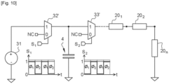
- FIG 8 schematically represents a third variant, 3d, of the memory writing device.
- This 3d writing device is similar to device 3a of the figure 1 , but its control module is configured in a particular way, and it further comprises a write detection and stop circuit 9.
- the write detection and stop circuit 9 is configured to detect a passage of the memory element 22 of the selected cell 20S, from its highly resistive state to its low resistive state, or vice versa. When this passage is detected, the write detection and stop circuit 9 emits a write detection signal, transmitted to the control module (not shown).
- control module it is configured to control the multiplexers 32' and 33' so as to execute steps a) and b) several times successively (otherwise formulated, so as to reproduce the phases ⁇ 1, then ⁇ 2 several times successively) so as to apply to the memory cell 20S a sequence of several successive write pulses (multiplus write technique). Furthermore, it is configured here to command a stoppage of this sequence of write pulses (by connecting the output of the multiplexer 33' to its unconnected input, for example), upon receipt of the write detection signal.
- connection device 5 of the memory can be configured to, in step b), connect the write capacitor 4 (or the write capacitors, if several capacitors are used, in parallel, or in alternation) with several memory cells 20 1 , 20 2 , ..., 20 n of the matrix, electrically connected in parallel with each other, as shown in the figure 9 .
- This write configuration is suitable for writing, in each of these cells, a highly resistive state (RESET).
- RESET highly resistive state
- connection device 5 may be present between these different cells.
- the memory connection device 5 can also be configured to, in step b), connect the write capacitor 4 (or the write capacitors, if several capacitors are used, in parallel, or alternately) with several memory cells 20 1 , 20 2 , ..., 20 n of the matrix, electrically connected in series with each other (or, optionally, to electrically connect the write capacitor 4 to a memory cell of the matrix 2 , as well as a cell memory of another matrix, these two memory cells being electrically connected in series one after the other).
- this write configuration is adapted to the writing, in each of these cells, of a low resistive state (SET).
Landscapes
- Engineering & Computer Science (AREA)
- Computer Hardware Design (AREA)
- Power Engineering (AREA)
- Chemical & Material Sciences (AREA)
- Crystallography & Structural Chemistry (AREA)
- Semiconductor Memories (AREA)
- Static Random-Access Memory (AREA)
- Read Only Memory (AREA)
Applications Claiming Priority (1)
| Application Number | Priority Date | Filing Date | Title |
|---|---|---|---|
| FR2113463A FR3130441B1 (fr) | 2021-12-14 | 2021-12-14 | Mémoire résistive à sélecteur, équipée d’un condensateur d’écriture, et procédé d’écriture associé |
Publications (1)
| Publication Number | Publication Date |
|---|---|
| EP4198985A1 true EP4198985A1 (de) | 2023-06-21 |
Family
ID=80595187
Family Applications (1)
| Application Number | Title | Priority Date | Filing Date |
|---|---|---|---|
| EP22212693.0A Pending EP4198985A1 (de) | 2021-12-14 | 2022-12-12 | Resistiver speicher mit selektor ausgestattet mit schreibkondensator und schreibverfahren dafür |
Country Status (3)
| Country | Link |
|---|---|
| US (1) | US12406724B2 (de) |
| EP (1) | EP4198985A1 (de) |
| FR (1) | FR3130441B1 (de) |
Citations (3)
| Publication number | Priority date | Publication date | Assignee | Title |
|---|---|---|---|---|
| US20090116280A1 (en) | 2007-11-07 | 2009-05-07 | Ovonyx, Inc. | Accessing a phase change memory |
| US8934280B1 (en) * | 2013-02-06 | 2015-01-13 | Crossbar, Inc. | Capacitive discharge programming for two-terminal memory cells |
| US20170139628A1 (en) * | 2015-11-13 | 2017-05-18 | SK Hynix Inc. | Electronic device |
Family Cites Families (1)
| Publication number | Priority date | Publication date | Assignee | Title |
|---|---|---|---|---|
| JP2011034637A (ja) * | 2009-08-03 | 2011-02-17 | Toshiba Corp | 不揮発性半導体記憶装置 |
-
2021
- 2021-12-14 FR FR2113463A patent/FR3130441B1/fr active Active
-
2022
- 2022-12-12 US US18/079,325 patent/US12406724B2/en active Active
- 2022-12-12 EP EP22212693.0A patent/EP4198985A1/de active Pending
Patent Citations (3)
| Publication number | Priority date | Publication date | Assignee | Title |
|---|---|---|---|---|
| US20090116280A1 (en) | 2007-11-07 | 2009-05-07 | Ovonyx, Inc. | Accessing a phase change memory |
| US8934280B1 (en) * | 2013-02-06 | 2015-01-13 | Crossbar, Inc. | Capacitive discharge programming for two-terminal memory cells |
| US20170139628A1 (en) * | 2015-11-13 | 2017-05-18 | SK Hynix Inc. | Electronic device |
Non-Patent Citations (3)
| Title |
|---|
| ROBAYO D ALFARO ET AL: "Integration of OTS based back-end selector with HfO2 OxRAM for crossbar arrays", 2019 IEEE 11TH INTERNATIONAL MEMORY WORKSHOP (IMW), IEEE, 12 May 2019 (2019-05-12), pages 1 - 4, XP033563797, DOI: 10.1109/IMW.2019.8739746 * |
| SEN ZHANG ET AL: "Programming resistive switching memory by a charged capacitor", APPLIED PHYSICS A; MATERIALS SCIENCE & PROCESSING, SPRINGER, BERLIN, DE, vol. 102, no. 4, 5 February 2011 (2011-02-05), pages 1003 - 1007, XP019890028, ISSN: 1432-0630, DOI: 10.1007/S00339-011-6320-5 * |
| TROTTI P ET AL: "Experimental Set-Up For Novel Energy Efficient Charge-based Resistive RAM (RRAM) Switching", 2020 IEEE 33RD INTERNATIONAL CONFERENCE ON MICROELECTRONIC TEST STRUCTURES (ICMTS), IEEE, 4 May 2020 (2020-05-04), pages 1 - 5, XP033777120, DOI: 10.1109/ICMTS48187.2020.9107936 * |
Also Published As
| Publication number | Publication date |
|---|---|
| FR3130441A1 (fr) | 2023-06-16 |
| FR3130441B1 (fr) | 2024-08-23 |
| US20230186987A1 (en) | 2023-06-15 |
| US12406724B2 (en) | 2025-09-02 |
Similar Documents
| Publication | Publication Date | Title |
|---|---|---|
| EP2951833B1 (de) | Programmierung von bipolarem widerstandsspeicher | |
| EP2509076B1 (de) | Elektronische Vorrichtung vom Typ Wählschalter | |
| FR2970592A1 (fr) | Cellule mémoire volatile/non volatile programmable | |
| FR3011117A1 (fr) | Procede et dispositif de commande d'une memoire reram | |
| US9142767B2 (en) | Resistive memory cell including integrated select device and storage element | |
| FR2970590A1 (fr) | Cellule mémoire volatile/non volatile sans charge | |
| FR2976711A1 (fr) | Cellule memoire avec memorisation volatile et non volatile | |
| EP0708447B1 (de) | Gegen Störungen unempfindlicher Speicher | |
| EP3154061A1 (de) | Verfahren und schaltkreis zur steuerung des stroms einer programmierung in einer nicht-flüchtigen speichermatrix | |
| FR2970593A1 (fr) | Cellule mémoire volatile/non volatile compacte | |
| EP4016531B1 (de) | Speicher mit einer matrix aus resistiven speicherzellen und entsprechendes schnittstellenverbindungsverfahren | |
| EP4198985A1 (de) | Resistiver speicher mit selektor ausgestattet mit schreibkondensator und schreibverfahren dafür | |
| EP4009371B1 (de) | Auswahlvorrichtung für resistive speichervorrichtung und entsprechendes herstellungsverfahren | |
| EP2987168B1 (de) | Speicherzelle mit nichtflüchtigem datenspeicher | |
| FR3118267A1 (fr) | Lecture différentielle de mémoire rram à faible consommation | |
| WO2003069630A2 (fr) | Cellule memoire a programmation unique non destructrice | |
| EP1420416B1 (de) | Dreiphasenspeicherzelle | |
| FR3025927A1 (fr) | Programmation de cellules anti-fusibles | |
| EP2977988B1 (de) | Nicht-flüchtiger speicher mit programmierbarem widerstand | |
| EP4055605A1 (de) | Selektive nichtflüchtige speichervorrichtung und zugehöriges leseverfahren | |
| EP1416498B1 (de) | Auf Speicherzellen basierter monotoner Zähler | |
| FR2549999A1 (fr) | Cellule de memoire du type ram comprenant un element de memoire non volatil electriquement programmable | |
| FR3125163A1 (fr) | Procede de lecture d’une rram multi-niveaux | |
| EP2987167B1 (de) | Nichtflüchtiger speicher | |
| FR3161303A1 (fr) | Mémoire résistive à accès aléatoire avec courant perturbateur réduit dans une architecture à cellule mémoire à ligne de source partagée |
Legal Events
| Date | Code | Title | Description |
|---|---|---|---|
| PUAI | Public reference made under article 153(3) epc to a published international application that has entered the european phase |
Free format text: ORIGINAL CODE: 0009012 |
|
| STAA | Information on the status of an ep patent application or granted ep patent |
Free format text: STATUS: REQUEST FOR EXAMINATION WAS MADE |
|
| 17P | Request for examination filed |
Effective date: 20221212 |
|
| AK | Designated contracting states |
Kind code of ref document: A1 Designated state(s): AL AT BE BG CH CY CZ DE DK EE ES FI FR GB GR HR HU IE IS IT LI LT LU LV MC ME MK MT NL NO PL PT RO RS SE SI SK SM TR |
|
| RBV | Designated contracting states (corrected) |
Designated state(s): AL AT BE BG CH CY CZ DE DK EE ES FI FR GB GR HR HU IE IS IT LI LT LU LV MC ME MK MT NL NO PL PT RO RS SE SI SK SM TR |
|
| RAP3 | Party data changed (applicant data changed or rights of an application transferred) |
Owner name: WEEBIT NANO LTD Owner name: COMMISSARIAT A L'ENERGIE ATOMIQUE ET AUX ENERGIESALTERNATIVES |