EP4198985A1 - Resistive memory with selector fitted with write capacitor and associated write method - Google Patents
Resistive memory with selector fitted with write capacitor and associated write method Download PDFInfo
- Publication number
- EP4198985A1 EP4198985A1 EP22212693.0A EP22212693A EP4198985A1 EP 4198985 A1 EP4198985 A1 EP 4198985A1 EP 22212693 A EP22212693 A EP 22212693A EP 4198985 A1 EP4198985 A1 EP 4198985A1
- Authority
- EP
- European Patent Office
- Prior art keywords
- write
- memory
- capacitor
- memory cell
- voltage
- Prior art date
- Legal status (The legal status is an assumption and is not a legal conclusion. Google has not performed a legal analysis and makes no representation as to the accuracy of the status listed.)
- Pending
Links
- 230000015654 memory Effects 0.000 title claims abstract description 283
- 239000003990 capacitor Substances 0.000 title claims abstract description 194
- 238000000034 method Methods 0.000 title claims description 9
- 239000011159 matrix material Substances 0.000 claims description 53
- 230000003071 parasitic effect Effects 0.000 claims description 25
- VNEBWJSWMVTSHK-UHFFFAOYSA-L disodium;3-hydroxynaphthalene-2,7-disulfonate Chemical compound [Na+].[Na+].C1=C(S([O-])(=O)=O)C=C2C=C(S([O-])(=O)=O)C(O)=CC2=C1 VNEBWJSWMVTSHK-UHFFFAOYSA-L 0.000 claims description 14
- 238000001514 detection method Methods 0.000 claims description 9
- 238000005516 engineering process Methods 0.000 description 9
- 235000021183 entrée Nutrition 0.000 description 7
- 244000045947 parasite Species 0.000 description 6
- 230000008859 change Effects 0.000 description 5
- 230000000694 effects Effects 0.000 description 4
- 238000004519 manufacturing process Methods 0.000 description 4
- 238000004513 sizing Methods 0.000 description 4
- 230000004075 alteration Effects 0.000 description 3
- 238000010586 diagram Methods 0.000 description 3
- 230000010354 integration Effects 0.000 description 3
- 239000000758 substrate Substances 0.000 description 3
- 102100023696 Histone-lysine N-methyltransferase SETDB1 Human genes 0.000 description 2
- 101710168120 Histone-lysine N-methyltransferase SETDB1 Proteins 0.000 description 2
- 239000000956 alloy Substances 0.000 description 2
- 229910045601 alloy Inorganic materials 0.000 description 2
- 230000007423 decrease Effects 0.000 description 2
- 229940082150 encore Drugs 0.000 description 2
- 238000005265 energy consumption Methods 0.000 description 2
- 230000006870 function Effects 0.000 description 2
- 238000011534 incubation Methods 0.000 description 2
- 238000005259 measurement Methods 0.000 description 2
- 229910052760 oxygen Inorganic materials 0.000 description 2
- 230000010287 polarization Effects 0.000 description 2
- 230000004044 response Effects 0.000 description 2
- 229910052710 silicon Inorganic materials 0.000 description 2
- 229910052717 sulfur Inorganic materials 0.000 description 2
- 239000010936 titanium Substances 0.000 description 2
- 241000287107 Passer Species 0.000 description 1
- XUIMIQQOPSSXEZ-UHFFFAOYSA-N Silicon Chemical compound [Si] XUIMIQQOPSSXEZ-UHFFFAOYSA-N 0.000 description 1
- RTAQQCXQSZGOHL-UHFFFAOYSA-N Titanium Chemical compound [Ti] RTAQQCXQSZGOHL-UHFFFAOYSA-N 0.000 description 1
- 229910052782 aluminium Inorganic materials 0.000 description 1
- 229910052787 antimony Inorganic materials 0.000 description 1
- 229910052785 arsenic Inorganic materials 0.000 description 1
- 230000000903 blocking effect Effects 0.000 description 1
- 238000004364 calculation method Methods 0.000 description 1
- 229910052799 carbon Inorganic materials 0.000 description 1
- 229910052798 chalcogen Inorganic materials 0.000 description 1
- 150000004770 chalcogenides Chemical class 0.000 description 1
- 239000004020 conductor Substances 0.000 description 1
- 238000000151 deposition Methods 0.000 description 1
- 238000007599 discharging Methods 0.000 description 1
- 239000006185 dispersion Substances 0.000 description 1
- 238000009826 distribution Methods 0.000 description 1
- 239000002019 doping agent Substances 0.000 description 1
- 230000005611 electricity Effects 0.000 description 1
- 238000013213 extrapolation Methods 0.000 description 1
- 238000007667 floating Methods 0.000 description 1
- 229910052733 gallium Inorganic materials 0.000 description 1
- 229910052732 germanium Inorganic materials 0.000 description 1
- 229910000449 hafnium oxide Inorganic materials 0.000 description 1
- WIHZLLGSGQNAGK-UHFFFAOYSA-N hafnium(4+);oxygen(2-) Chemical compound [O-2].[O-2].[Hf+4] WIHZLLGSGQNAGK-UHFFFAOYSA-N 0.000 description 1
- CJNBYAVZURUTKZ-UHFFFAOYSA-N hafnium(IV) oxide Inorganic materials O=[Hf]=O CJNBYAVZURUTKZ-UHFFFAOYSA-N 0.000 description 1
- 238000010438 heat treatment Methods 0.000 description 1
- 230000000977 initiatory effect Effects 0.000 description 1
- 239000012212 insulator Substances 0.000 description 1
- 230000005415 magnetization Effects 0.000 description 1
- 239000000463 material Substances 0.000 description 1
- 238000004377 microelectronic Methods 0.000 description 1
- 229910052757 nitrogen Inorganic materials 0.000 description 1
- 230000010355 oscillation Effects 0.000 description 1
- 230000003534 oscillatory effect Effects 0.000 description 1
- 239000001301 oxygen Substances 0.000 description 1
- -1 oxygen chalcogen Chemical class 0.000 description 1
- 230000009467 reduction Effects 0.000 description 1
- 229910052711 selenium Inorganic materials 0.000 description 1
- 239000010703 silicon Substances 0.000 description 1
- 238000004088 simulation Methods 0.000 description 1
- 229910052714 tellurium Inorganic materials 0.000 description 1
- 229910052719 titanium Inorganic materials 0.000 description 1
- 230000007704 transition Effects 0.000 description 1
- 229910052725 zinc Inorganic materials 0.000 description 1
Images


Classifications
-
- G—PHYSICS
- G11—INFORMATION STORAGE
- G11C—STATIC STORES
- G11C13/00—Digital stores characterised by the use of storage elements not covered by groups G11C11/00, G11C23/00, or G11C25/00
- G11C13/0002—Digital stores characterised by the use of storage elements not covered by groups G11C11/00, G11C23/00, or G11C25/00 using resistive RAM [RRAM] elements
- G11C13/0021—Auxiliary circuits
- G11C13/0069—Writing or programming circuits or methods
-
- G—PHYSICS
- G11—INFORMATION STORAGE
- G11C—STATIC STORES
- G11C11/00—Digital stores characterised by the use of particular electric or magnetic storage elements; Storage elements therefor
- G11C11/02—Digital stores characterised by the use of particular electric or magnetic storage elements; Storage elements therefor using magnetic elements
- G11C11/16—Digital stores characterised by the use of particular electric or magnetic storage elements; Storage elements therefor using magnetic elements using elements in which the storage effect is based on magnetic spin effect
- G11C11/165—Auxiliary circuits
- G11C11/1659—Cell access
-
- G—PHYSICS
- G11—INFORMATION STORAGE
- G11C—STATIC STORES
- G11C11/00—Digital stores characterised by the use of particular electric or magnetic storage elements; Storage elements therefor
- G11C11/02—Digital stores characterised by the use of particular electric or magnetic storage elements; Storage elements therefor using magnetic elements
- G11C11/16—Digital stores characterised by the use of particular electric or magnetic storage elements; Storage elements therefor using magnetic elements using elements in which the storage effect is based on magnetic spin effect
- G11C11/165—Auxiliary circuits
- G11C11/1675—Writing or programming circuits or methods
-
- G—PHYSICS
- G11—INFORMATION STORAGE
- G11C—STATIC STORES
- G11C11/00—Digital stores characterised by the use of particular electric or magnetic storage elements; Storage elements therefor
- G11C11/02—Digital stores characterised by the use of particular electric or magnetic storage elements; Storage elements therefor using magnetic elements
- G11C11/16—Digital stores characterised by the use of particular electric or magnetic storage elements; Storage elements therefor using magnetic elements using elements in which the storage effect is based on magnetic spin effect
- G11C11/165—Auxiliary circuits
- G11C11/1693—Timing circuits or methods
-
- G—PHYSICS
- G11—INFORMATION STORAGE
- G11C—STATIC STORES
- G11C11/00—Digital stores characterised by the use of particular electric or magnetic storage elements; Storage elements therefor
- G11C11/02—Digital stores characterised by the use of particular electric or magnetic storage elements; Storage elements therefor using magnetic elements
- G11C11/16—Digital stores characterised by the use of particular electric or magnetic storage elements; Storage elements therefor using magnetic elements using elements in which the storage effect is based on magnetic spin effect
- G11C11/165—Auxiliary circuits
- G11C11/1697—Power supply circuits
-
- G—PHYSICS
- G11—INFORMATION STORAGE
- G11C—STATIC STORES
- G11C13/00—Digital stores characterised by the use of storage elements not covered by groups G11C11/00, G11C23/00, or G11C25/00
- G11C13/0002—Digital stores characterised by the use of storage elements not covered by groups G11C11/00, G11C23/00, or G11C25/00 using resistive RAM [RRAM] elements
- G11C13/0004—Digital stores characterised by the use of storage elements not covered by groups G11C11/00, G11C23/00, or G11C25/00 using resistive RAM [RRAM] elements comprising amorphous/crystalline phase transition cells
-
- G—PHYSICS
- G11—INFORMATION STORAGE
- G11C—STATIC STORES
- G11C13/00—Digital stores characterised by the use of storage elements not covered by groups G11C11/00, G11C23/00, or G11C25/00
- G11C13/0002—Digital stores characterised by the use of storage elements not covered by groups G11C11/00, G11C23/00, or G11C25/00 using resistive RAM [RRAM] elements
- G11C13/0021—Auxiliary circuits
- G11C13/003—Cell access
-
- G—PHYSICS
- G11—INFORMATION STORAGE
- G11C—STATIC STORES
- G11C13/00—Digital stores characterised by the use of storage elements not covered by groups G11C11/00, G11C23/00, or G11C25/00
- G11C13/0002—Digital stores characterised by the use of storage elements not covered by groups G11C11/00, G11C23/00, or G11C25/00 using resistive RAM [RRAM] elements
- G11C13/0021—Auxiliary circuits
- G11C13/0038—Power supply circuits
-
- G—PHYSICS
- G11—INFORMATION STORAGE
- G11C—STATIC STORES
- G11C13/00—Digital stores characterised by the use of storage elements not covered by groups G11C11/00, G11C23/00, or G11C25/00
- G11C13/0002—Digital stores characterised by the use of storage elements not covered by groups G11C11/00, G11C23/00, or G11C25/00 using resistive RAM [RRAM] elements
- G11C13/0021—Auxiliary circuits
- G11C13/0061—Timing circuits or methods
-
- G—PHYSICS
- G11—INFORMATION STORAGE
- G11C—STATIC STORES
- G11C5/00—Details of stores covered by group G11C11/00
- G11C5/14—Power supply arrangements, e.g. power down, chip selection or deselection, layout of wirings or power grids, or multiple supply levels
- G11C5/147—Voltage reference generators, voltage or current regulators; Internally lowered supply levels; Compensation for voltage drops
-
- G—PHYSICS
- G11—INFORMATION STORAGE
- G11C—STATIC STORES
- G11C2213/00—Indexing scheme relating to G11C13/00 for features not covered by this group
- G11C2213/70—Resistive array aspects
- G11C2213/76—Array using an access device for each cell which being not a transistor and not a diode
-
- H—ELECTRICITY
- H10—SEMICONDUCTOR DEVICES; ELECTRIC SOLID-STATE DEVICES NOT OTHERWISE PROVIDED FOR
- H10B—ELECTRONIC MEMORY DEVICES
- H10B63/00—Resistance change memory devices, e.g. resistive RAM [ReRAM] devices
- H10B63/20—Resistance change memory devices, e.g. resistive RAM [ReRAM] devices comprising selection components having two electrodes, e.g. diodes
- H10B63/24—Resistance change memory devices, e.g. resistive RAM [ReRAM] devices comprising selection components having two electrodes, e.g. diodes of the Ovonic threshold switching type
-
- H—ELECTRICITY
- H10—SEMICONDUCTOR DEVICES; ELECTRIC SOLID-STATE DEVICES NOT OTHERWISE PROVIDED FOR
- H10B—ELECTRONIC MEMORY DEVICES
- H10B63/00—Resistance change memory devices, e.g. resistive RAM [ReRAM] devices
- H10B63/80—Arrangements comprising multiple bistable or multi-stable switching components of the same type on a plane parallel to the substrate, e.g. cross-point arrays
Definitions
- the technical field is that of micro-electronics, more particularly that of resistive memories.
- the invention relates in particular to a particular writing device, making it possible to write one or more data in such a resistive memory.
- a memory of this type generally comprises a matrix of memory cells, sometimes called “memory points”, each storing a datum, for example a binary datum.
- the binary data in question is represented by the level of resistance, either high or low, of the memory cell considered.
- the data stored in such a memory cell can also be data that can take on more than two different values (for example four different values, the data then grouping together two bits), in the case of a “multilevel” memory cell.
- the memory cell has a resistance equal to one of its resistance levels (the number of which is greater than two), which level is associated with the value stored in the cell.
- memory cells may for example be memory cells of the filamentary type, comprising an active layer in which an electrically conductive filament is either broken, or on the contrary reformed to vary the level of resistance of the memory cell, during write cycles. then resetting this cell to zero (SET operations, when the filament is reformed, and RESET operations, when the filament is broken again).
- a memory cell, of the filament type can for example be a cell of the OxRam type (according to the Anglo-Saxon acronym for “Oxide Random Access Memory”), or of the CB-RAM type (according to the Anglo-Saxon acronym for “Conductive Bridge Random Access Memory”).
- the resistive memory cells in The question may also be cells of the PCRAM (for “Phase Change Random Access Memory”) type, in which an amorphous-crystalline phase change is accompanied by a change in the resistance of the cell.
- the write voltage In order to be able to write the memory cell considered properly, the write voltage must then be applied in the form of a pulse in the form of a slot, of relatively long duration (longer than the maximum value expected for the incubation period).
- a SET that is to say in a case where the memory cell is brought into its low resistive state, the moment from which the cell becomes fairly strongly conductive can be located either at the start of this impulse, or rather at the end of it.
- a noticeable electric current passes through the memory cell for a significant duration (i.e.: for almost the entire duration of the write pulse). This results in high power consumption, and can also cause a form of alteration or small-scale mechanical tensions (a "stress") within the memory cell.
- one solution consists of an active write detection and stop circuit (sometimes called "write termination"), which detects the passage from a highly resistive state to a low resistive, for the cell to be written, and which stops the write pulse as soon as this passage has been detected.
- write termination an active write detection and stop circuit
- the energy consumed during writing is intrinsically limited (by the energy initially stored in the capacitor, during step a) of charging).
- the passage of electric current in the memory cell, during the write operation naturally (and in a way, automatically) leads to a decrease in the voltage applied to the memory cell, due to the discharge of the write capacitor. in the memory cell, thus avoiding electrical overconsumption, even if the moment of switching from the highly resistive state to the low resistive state (or vice versa) is partly unpredictable.
- BEOL Back-End-Of-Line
- FEOL Front-End-Of-Line
- Such a selector can be formed of layers deposited on or under a memory layer, and engraved in block at the same time as the memory layer (which allows self-alignment of the selector and the memory element), hence the name co-integrable (since they are integrated in the same level, in terms of manufacturing technology).
- the limitation of the energy consumed comes both from the use of the write capacitor (as explained above), but also from the use of this selector, which, in a particularly simple, and in combination with this capacitor, plays the role of a write detection and stop circuit in a way, due to the blocking of the selector when the current which passes through it becomes lower than the holding current of the selector which was mentioned above.
- This type of selector with double threshold is for example an OTS type selector.
- the OTS type selector has two terminals and, therefore, is operated differently from the OTS type selector described in the document US2009/0116280A1 which is itself with three terminals. The writing issues are therefore different.
- threshold selectors can block (if the conditions for maintaining the conductive state - that is to say in the on state - are not satisfied; in particular if the current which crosses the 1S1R cell becomes lower than the holding current), then, under the effect of a recharge of the parasitic capacitances, unblocking (if the voltage at the terminals of the 1S1R cell becomes greater than its threshold voltage V th,1S1R ), to re-block again,
- the capacitance values to be used turn out to be sufficiently small not to significantly increase the size of a crossbar type memory matrix.
- the write capacitor used in steps a) and b) may have an electrical capacitance greater than or equal to the electrical capacitance C o.1 defined by formula (F1) above.
- the present technology relates in particular to a memory, comprising at least one, here several resistive memory cells, and comprising a capacitor writing device for programming these memory cells, that is to say for writing data in these cells.
- THE figure 6 , 7 And 8 schematically represent three variants 3b, 3c and 3d of the writing device 3a of the figure 1 .
- Each of these variants can equip memory 1 of the figure 1 , in place of the writing device 3a.
- the memory 1 will be described first of all in a general way, as a whole, as well as the principle of operation of its writing device. The sizing of the write capacitor(s) will then be presented in more detail. Finally, the variants of the writing device 3b, 3c and 3d, as well as particular connection modes of the memory cells to be programmed will be described, with reference to the figures 6 to 10 .
- the matrix 2 comprises n electrical row tracks 23, and m electrical column tracks 24, for example metallic.
- the memory cells 20, m ⁇ n in number, are located at the intersections between the row electric tracks and the column electric tracks.
- m and n can be equal to 128.
- the memory cells 20 of the array are of the same type (they are manufactured together, in the same way, and therefore have the same characteristics, or very close characteristics) .
- Each memory cell 20 is connected between, on the one hand, one of the row electric tracks and, on the other hand, one of the column electric tracks.
- an electric voltage V for example a write voltage
- this electrical voltage between this row electrical track, and this column electrical track.
- the matrix 2, and more generally the memory 1 can be produced by planar techniques, in the form of a stack of several etched and functionalized layers. As shown schematically in the picture 2 , the row electric tracks 23 can then be located in a lower layer while the column electric tracks 24 are located in an upper layer (or vice versa), the memory cells 20 (also called memory points) then extending between this lower layer and this upper layer.
- This type of matrix is often referred to as a "crossbar" type matrix in this technical field.
- the resistive element 22 In its low resistive state, the resistive element 22 has a low electrical resistance, denoted R SET , and in its high resistive state, it has a high electrical resistance, denoted RRESET.
- a datum can be written and stored in each memory cell 20, this datum being represented by the resistance level of the memory element 22.
- the data in question is binary data, and the memory cells are programmed so as to place their respective memory elements 22 either in their highly resistive state or in their low resistive state.
- multilevel elements it would be possible to use more than two distinct resistance levels, for each memory element (“multilevel” elements), so as to store in each cell a datum likely to take on more than two different values.
- the present technology based in particular on a write capacitor, is presented below in the case of two-level memory elements but it can also be applied to multilevel memory cells as mentioned above.
- the memory element 22 is of the OxRAM type.
- it could also be a memory element of the CB-RAM, PCRAM, MRAM type (for "Magnetic RAM” in English, where the relative magnetization is implemented between a reference magnetic layer and a programmable magnetic layer), or, more generally, of the ReRAM type.
- Each memory cell 20 comprises, in addition to the memory element 22, a selector 21 arranged in series with the memory element 22 ( picture 2 ). From an electrical point of view, the selector 21 and the memory element are connected in series, one after the other, between the two corresponding tracks 23, 24.
- the memory cells are of the “1S1R” type, here.
- These selectors 21 are switching elements. They make it possible to reduce the leakage currents passing through the cells which are not being read or written at the instant in question. These are selectors 21 with thresholds.
- Each selector 21 becomes electrically conductive, that is to say switches to the on state, when the voltage at its terminals becomes greater than a threshold voltage V th . Furthermore, the selectors 21 are of the holding threshold type: each selector switches back to the blocked state if the current passing through it becomes less than a holding current I h .
- the selectors 21 are so-called “back-end” selectors. They are made by depositing layers, which can be deposited almost at the same manufacturing stages as the layer or layers of the memory elements 22. Furthermore, the layer or layers of such a selector can be etched at the same time as those of the corresponding memory element, jointly (during the same burning operation), which facilitates the production of the memory and makes it possible to reduce the dimensions of the memory cell 20 to a minimum.
- These “backend” selectors 21 may be, for example, selectors of the MIT (“metal-insulator transition switch”) type.
- the selectors 21 can also, as here, be selectors of the OTS type (for “Ovonic Threshold Switch”, or ovonic threshold switch).
- OTS type selectors are threshold switches made from chalcogenide alloy films, such an alloy being composed of a non-oxygen chalcogen element (S, Se, Te), alloyed with elements such as Ge, Si, Sb, As, Al, Zn, Ga. They can be doped with light elements such as B, C, N, O, P (with dopant concentrations which can be greater than 1 atomic%).
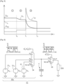
- This figure shows the electric current i which passes through the element considered (expressed in arbitrary units) as a function of the voltage U applied to its terminals (also in arbitrary units).
- the measurement points i 1R,SET and i 1R,RESET correspond to the memory element 22 alone, respectively in its low resistive state and in its highly resistive state.
- Measurement points i 1R1S,SET and i 1R1S,RESET correspond to the entire memory cell, when the memory element 22 is, respectively, in its low resistive state and in its high resistive state.
- the resistance of the memory element 22 (in its lowly resistive state), R SET (for example of the order of a few kilohms or possibly, of the order of ten or a few tens of kilohms, depending the technology used), is much smaller than that of the selector (the resistance of the selector, just below the selector threshold voltage V th , is typically of the order of one megohm).
- Most of the voltage U applied to the memory cell 20 is therefore found at the terminals of the selector 21 (the voltage U is distributed mainly to the terminals of the selector).
- Memory cell threshold voltage V th SET is therefore very close to the threshold voltage of the selector V th .
- the overall resistance of the memory cell 20 after the selector has switched to the on state can be expressed as RSET + R sel where R sel is a resistance (effective resistance) of the selector 21 in the on state (by example of the order of a kilohm).
- FIG 4 schematically represents the current-voltage characteristic of any one of the selectors 21.
- the voltage U 21 applied to the selector corresponds to the abscissa axis, while the ordinate axis corresponds to the current i which crosses the selector (in logarithmic scale).
- the selector 21 when the selector 21 is in the on state, if the current passing through it becomes less than a holding current I h , then the selector switches back to the off state.
- the corresponding voltage, at the terminals of the selector, just before it relocks, is called the selector holding voltage V h,sel .
- the memory 1 also includes a connection device 5, configured to selectively connect, that is to say to address one of the memory cells 20 of the matrix 2 (for example the cell marked with the reference 20S, on there figure 1 ), to the writing device 3a (or, alternatively, 3b, 3c, or 3d) of the memory.
- a connection device 5 configured to selectively connect, that is to say to address one of the memory cells 20 of the matrix 2 (for example the cell marked with the reference 20S, on there figure 1 ), to the writing device 3a (or, alternatively, 3b, 3c, or 3d) of the memory.
- connection device 5 thus makes it possible to select the cell to be programmed (in the example of the figure 1 , the cell selected is cell 20S), and to connect this cell (but not the others) to the writing device.
- connection device 5 can also be configured to connect a given group of memory cells of the matrix (i.e.: a given subset of memory cells of the matrix) to the writing device.
- connection device can for example comprise several controllable switches (such as transistors), for example one for each row electric track 23 (at the end of the track), and one for each column electric track 24 (at the end of the track) .
- controllable switches such as transistors
- connection device 5 can also be configured to bias the entire matrix 2 according to a given electrical bias configuration, when writing (or reading) the selected memory cell(s) 20S.
- this second switching element can either be part of the connection device 5 (i.e.: be integrated directly into the switching device 5), or be separate from the latter.
- the charging device 30a; 30b; 30c; 30d is therefore configured to, during the write step b), disconnect the capacitor from the source.
- the charging device 30a of the writing device 3a comprises the voltage source 31 mentioned above (this voltage source delivers for example a voltage equal to the initial writing voltage Vinit), and the first switching element, 32 .
- a first output terminal of source 31 is connected to a first terminal of write capacitor 4, for example directly (that is to say by an electrical conductor, without intermediate component), while the second output terminal of the source is connected to the second terminal of capacitor 4 via first switching element 32.
- the first switching element 32 is for example a transistor can also be a multiplexer, such as multiplexer 32 'of the figure 8 or 9 , having for example two inputs and one output.
- the output of the multiplexer is connected to one of the two terminals of the write capacitor, one of the inputs of the multiplexer is connected to the second terminal of the source, and the other input of the multiplexer (marked by the acronym NC in the figures) is not connected.
- the first terminal of the write capacitor 4 is also connected to the connection device 5 of the matrix 2, for example directly, while the second terminal of this capacitor is connected to this connection device via the second element of switching 33.
- the second switching element can also be a transistor, for example, or a multiplexer, such as the multiplexer 33 'of the figure 8 , also having an output (connected to the connection device 5) and at least two inputs, one connected to the second terminal of the capacitor 4, and the other unconnected.
- FIG. 5 schematically shows the evolution, over time t, of the voltage U 4 across the terminals of a write capacitor 4, during a write operation of a low resistive state (SET) in the memory cell 20S of the memory 1.
- the evolution over time of the electric current i 20 passing through the memory cell is also represented.
- the write capacitor 4 is charged beforehand, to the initial write voltage Vinit, during a first phase (phase “1”, on the figure 5 ). At the end of this first phase, at time t o , write capacitor 4 is connected to selected cell 20S (by controlling second switching element 32 and connection device 5 for this purpose).
- the electric charge initially contained in the write capacitor 4 begins by being distributed between this capacitor and the parasitic capacitance C by (parasitic capacitance of the matrix 2, and of the electrical circuit elements which connect it to the write capacitor ), during a second phase (phase “2” in the figures).
- capacitor 4 partially discharges into memory cell 20S, which makes it possible to provide memory element 22 with sufficient energy to make it pass from its highly resistive state to its low resistive state. .
- the voltage U 4 at the terminals of the write capacitor decreases, as does the current i 20 flowing through the memory cell.
- current i 20 becomes lower than holding current I h (at time t2, on the figure 5 )
- the selector switches back to its blocked state, which marks the end of this third phase.
- the discharge of write capacitor 4 then stops (and current i 20 drops significantly).
- the voltage across write capacitor 4, at the end of this third phase, is called end-of-write voltage V stop .
- the write end voltage V stop can therefore also be expressed as V h,sel +R by ⁇ I h +R SET ⁇ I h where V h,sel is the holding voltage of selector 21 alone (see the figure 4 ), in a case where the (total) leakage current I leak which crosses the other memory cells, not selected, is negligible. If this is not the case, the end-of-write voltage V stop can be expressed, more precisely, as V h,sel +R by ⁇ (I h +I leak )R SET ⁇ I h .
- the fact that the selector relocks when the current becomes lower than the holding current I h may seem problematic at first sight, since this limits the electrical energy that can be transmitted to the memory element. during this discharge (thereby risking preventing a suitable writing of this element). But in fact, by sizing the capacitor 4 and the voltage source 31 in an ad-hoc manner, as explained below, it is possible to transmit to the memory element sufficient energy to carry out this writing successfully, before the selector does not relock. The reblocking effect of the selector then makes it possible to limit the energy consumed for this writing (and the possible effects of undesirable heating of the memory element), by preventing a complete discharge of the capacitor.
- this arrangement with write capacitor and selector at reblocking is therefore even more efficient than a solution which would be based solely on a write capacitor (a solution which would however already be significantly more efficient than a write performed directly from a voltage source, without a write capacitor limiting total energy consumed).
- the value of its capacitance C is chosen in particular according to the electrical energy E SET to be supplied to the memory element 22 to make it pass from its highly resistive state to its low resistive state. .
- the inventors have in fact observed that, as long as the selector is in its on state, a write operation of a SET state is generally carried out successfully provided that the electrical energy communicated to the memory cell is greater than or equal to at a given energy level, which is precisely the energy E SET in question.
- the energy E SET can therefore be the minimum energy, required on average to change the memory element from its RESET state to its SET state (average over several memory elements of the same type, for example, or average over several successive operations writing a SET state, on the same memory element).
- E SET can be the energy beyond which the proportion (otherwise formulated, the probability) of success of the RESET->SET write operation is greater than a given threshold, for example, greater than 90% , or 95% (instead of just above 50%).
- E SET can be the energy beyond which the success of the RESET->SET write operation is considered almost certain (which corresponds for example to a success threshold of 99%, or more ; in this case, the value of E SET can be obtained by extrapolation, from a distribution of the energy value consumed for several write operations).
- the energy E SET is the limit energy, for which this proportion of success is reached, for a given writing protocol (indeed, the proportion of success may depend on the writing protocol used, such a protocol being defined by : the use of a single pulse, or on the contrary of several successive pulses; and/or by the shape, the amplitude, and/or the duration of the pulse(s).
- the protocol corresponding to the value of E SET in question, is a protocol having characteristics corresponding (for example identical) to the characteristics of the write operation carried out with the present capacitor writing device 4.
- the energy E SET can be determined from tests carried out on one or more memory elements 22 of the type considered.
- the capacitance C of the write capacitor 4 can also be chosen taking into account the parasitic capacitance C par mentioned above (parasitic capacitance of the matrix 2, and of the electrical circuit elements which connect it to the write capacitor 4).
- the parasitic resistance R par is for example equal to the sum of these three contributions.
- the leakage resistance R leak is for example equal to the individual leakage resistance of a memory cell 20 having its selector blocked, divided by m+n-2 (because m+n-2 such individual leakage resistances are connected in parallel to each other). But it may be different, depending on the bias configuration used to bias the matrix 2 when writing the considered memory cell 20S (ie: depending on whether it is the "V/2" bias configuration, or another polarization configuration).
- the effective capacitance C par,mat of the matrix portion in question takes into account both the parasitic capacitances of the electrical row track 23 and of the electrical column track 24 considered, and the electrical capacitances of the stacks of the non-selected memory cells of this row and column. It can therefore be expressed as m+n-1 times the individual parasitic capacitance of a "non-selected" memory cell, in the "V/2" polarization configuration (it can however have a different value, for other matrix bias configurations).
- the individual parasitic capacitance of an "unselected” memory cell includes both the capacitance of the stack formed by the selector and the memory element (MIM stack), and the capacitance of the small track portions associated with this memory cell. (Located in the immediate vicinity of this cell; these portions being the track elements repeated m ⁇ n times to form the set of row and column electrical tracks). This individual parasitic capacitance is therefore the total capacitance of a “bitcell” of the matrix.
- the three estimates C o,1 , C o,2 , C o,3 of the minimum value to be given to the capacitance C are ordered as follows: C o,1 ⁇ C o,2 ⁇ C o,3 , and the C o,3 estimate is the most accurate.
- the values of C o.2 and of C o.3 may turn out to be close to each other.
- the capacitance C of the write capacitor 4 can for example be between once C o.2 and twice C o.2 (or, alternatively, between once C o.2 and three times C o.2 ).
- the fact that it is greater than C o.2 makes it possible to transmit sufficient energy to the memory cell 20s to write the state SET, with a high probability of success.
- the fact that it is less than two or three times C o.2 makes it possible to limit the electrical energy consumed during this operation, by remaining close to the energy E SET just necessary to carry out this writing (this also allows to limit the dimensions of the write capacitor to what is necessary for this write operation).
- the capacitance C of the write capacitor 4 could be between once C o.3 and twice C o.3 , or between once C o.3 and three times C o.3 .
- the initial write voltage Vinit it may be interesting to choose it relatively high (while remaining compatible with the type of memory cell and the integration technology used), because this then makes it possible to reach the energy E SET necessary for writing even with a write capacitor of limited capacitance (otherwise formulated, the minimum capacitance C o.1 , C o.2 or even C o.3 is all the smaller as Vinit is large).
- high write voltage can lead to higher write success rate and speed.
- the initial write voltage Vinit is chosen equal to 4.6 volts, in this example.
- the write end voltage V stop it is approximately 1 Volt.
- the capacitance C of the write capacitor 4 can for example be chosen equal to 2 pF (in fact, for these parameters, C 0.3 is approximately 2 pF).
- digital simulations of electrical response show that the total energy cost of the write operation of this SET state is 15 pJ, and that the duration of phase 3 described above is approximately 25 ns.
- the energy consumption E of the write operation is 0.6 ⁇ t AS (ns), where t AS is the time during which the write pulse continues to be applied, after switching of the selector to the passing state.
- the capacitance values C suitable for the write capacitor turn out to be typically between 1 and 10 pF, or possibly between 1 and 100 pF (depending on the type of memory cells used, and according to the dimensions of the matrix). Given these values, the write capacitor can be conveniently integrated into the memory, occupying an area of the order of 0.1 ⁇ 0.1 mm 2 or less. By way of example, for the capacitance of 2 pF mentioned above, integration over an area of around 20 ⁇ m ⁇ 25 ⁇ m is possible with the capacitor integration technologies currently available. In practice, the area needed to make the write capacitor is comparable to, or even less than, the area occupied by matrix 2, so that the write capacitor can for example be made on or under the matrix, directly above the latter.
- memory 1 has been presented in detail above in the case of writing a state SET (low resistance).
- This memory, and its writing device can however also be used for writing from a highly resistive state (RESET), that is to say to change a memory element 22 from its low resistive state to its highly resistive state.
- RESET highly resistive state
- the problem of electrical overconsumption arises in a comparable manner when writing a RESET state. Indeed, once the selector has switched to the on state, and even if the memory element has switched to its highly resistive state, a non-negligible electric current passes through the memory cell for the remaining duration of the power pulse. writing.
- FIG 6 schematically represents a first variant 3b of the writing device 3a of the figure 1 .
- This selector also includes an unconnected in o input. It makes it possible to selectively (alternatively) connect one or the other of said sources to the write capacitor 4, or to disconnect the capacitor 4 from these sources (by connecting it to the unconnected in o input). This arrangement thus makes it possible to adjust on controls the voltage under which capacitor 4 is charged, and therefore the initial write voltage V init .
- the second switching element which connects the write capacitor to the write cell 20S, is made in the form of a multiplexer 35 with two inputs (in o and in 1 ).
- FIG 7 schematically represents a second variant 3c of the writing device 3a of the figure 1 .
- the control module of the writing device 3c (not represented), which produces the control signals S i 0 :S i n and S° 0 :S° n of the multiplexers 36 and 37, can be configured to control these multiplexers according to two successive phases ⁇ 1 and ⁇ 2 repeated several times in succession (see the figure 7 ).
- capacitors 4, 4 2 , ..., 4 n are all disconnected from memory cell 20S. And one or more of these capacitors are connected to the source 31, to charge this or these capacitors. Then, during the second phase ⁇ 2, the capacitor or capacitors charged during the previous phase ⁇ 1 are disconnected from the source 31, and connected to the cell 20S to write this cell.
- this writing device 3c therefore makes it possible to modify, on command, the value of the electrical capacitance used during the writing operation, either by selecting one or the other of the capacitors 4, 4 2 , ..., 4 n (which can have different electrical capacities, either by connecting, in parallel, more or less of these write capacitors.
- This arrangement makes it possible, in a way, to have an equivalent capacitor of large capacity, without however being limited by a time of Important (pre)charge, thanks to the bearing set up between these different capacitors 4, 4 2 , ..., 4 n .
- This arrangement makes it possible to limit the dead times linked to the charging of the write capacitor(s).
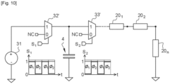
- FIG 8 schematically represents a third variant, 3d, of the memory writing device.
- This 3d writing device is similar to device 3a of the figure 1 , but its control module is configured in a particular way, and it further comprises a write detection and stop circuit 9.
- the write detection and stop circuit 9 is configured to detect a passage of the memory element 22 of the selected cell 20S, from its highly resistive state to its low resistive state, or vice versa. When this passage is detected, the write detection and stop circuit 9 emits a write detection signal, transmitted to the control module (not shown).
- control module it is configured to control the multiplexers 32' and 33' so as to execute steps a) and b) several times successively (otherwise formulated, so as to reproduce the phases ⁇ 1, then ⁇ 2 several times successively) so as to apply to the memory cell 20S a sequence of several successive write pulses (multiplus write technique). Furthermore, it is configured here to command a stoppage of this sequence of write pulses (by connecting the output of the multiplexer 33' to its unconnected input, for example), upon receipt of the write detection signal.
- connection device 5 of the memory can be configured to, in step b), connect the write capacitor 4 (or the write capacitors, if several capacitors are used, in parallel, or in alternation) with several memory cells 20 1 , 20 2 , ..., 20 n of the matrix, electrically connected in parallel with each other, as shown in the figure 9 .
- This write configuration is suitable for writing, in each of these cells, a highly resistive state (RESET).
- RESET highly resistive state
- connection device 5 may be present between these different cells.
- the memory connection device 5 can also be configured to, in step b), connect the write capacitor 4 (or the write capacitors, if several capacitors are used, in parallel, or alternately) with several memory cells 20 1 , 20 2 , ..., 20 n of the matrix, electrically connected in series with each other (or, optionally, to electrically connect the write capacitor 4 to a memory cell of the matrix 2 , as well as a cell memory of another matrix, these two memory cells being electrically connected in series one after the other).
- this write configuration is adapted to the writing, in each of these cells, of a low resistive state (SET).
Landscapes
- Engineering & Computer Science (AREA)
- Computer Hardware Design (AREA)
- Power Engineering (AREA)
- Chemical & Material Sciences (AREA)
- Crystallography & Structural Chemistry (AREA)
- Semiconductor Memories (AREA)
- Read Only Memory (AREA)
- Static Random-Access Memory (AREA)
Abstract
Une telle mémoire (1), comprenant au moins une cellule (20) mémoire résistive et un dispositif d'écriture (3a). La cellule mémoire (20) comprend un élément mémoire (22) ayant au moins un état hautement résistif et un état bassement résistif, et un sélecteur (21) agencé en série avec l'élément mémoire, le sélecteur étant électriquement conducteur lorsqu'une tension supérieure à une tension seuil (V<sub>th</sub>) donnée est appliquée au sélecteur. Le dispositif d'écriture comprend au moins un condensateur d'écriture (4) et un dispositif de charge (30a), et est configuré pour charger le condensateur d'écriture puis pour le connecter à la cellule mémoire pour programmer cette cellule.Such a memory (1), comprising at least one resistive memory cell (20) and a write device (3a). The memory cell (20) comprises a memory element (22) having at least a high resistive state and a low resistive state, and a selector (21) arranged in series with the memory element, the selector being electrically conductive when a voltage greater than a given threshold voltage (V<sub>th</sub>) is applied to the selector. The write device comprises at least one write capacitor (4) and a charging device (30a), and is configured to charge the write capacitor and then to connect it to the memory cell to program this cell.
Description
Le domaine technique est celui de la micro-électronique, plus particulièrement celui des mémoires résistives.The technical field is that of micro-electronics, more particularly that of resistive memories.
L'invention concerne notamment un dispositif d'écriture particulier, permettant d'écrire une ou des données dans une telle mémoire résistive.The invention relates in particular to a particular writing device, making it possible to write one or more data in such a resistive memory.
De nouveaux types de mémoires non volatiles, appelées mémoires résistives, ou parfois ReRAM (selon l'acronyme de « Resistive Random Access Memory »), ont été développés ces dernières années. Une mémoire de ce type comprend généralement une matrice de cellules mémoires, parfois appelées « points mémoire », stockant chacune une donnée, par exemple une donnée binaire. La donnée binaire en question est représentée par le niveau de résistance, soit haut, soit bas, de la cellule mémoire considérée. La donnée stockée dans une telle cellule mémoire peut aussi être une donnée pouvant prendre plus de deux valeurs différentes (par exemple quatre valeurs différentes, la donnée regroupant alors deux bits), dans le cas d'une cellule mémoire « multiniveaux ». Dans ce cas, la cellule mémoire présente une résistance égale à l'un de ses niveaux de résistance (dont le nombre est supérieur à deux), niveau qui est associé à la valeur stockée dans la cellule.New types of nonvolatile memory, called resistive memory, or sometimes ReRAM (from the acronym for "Resistive Random Access Memory"), have been developed in recent years. A memory of this type generally comprises a matrix of memory cells, sometimes called “memory points”, each storing a datum, for example a binary datum. The binary data in question is represented by the level of resistance, either high or low, of the memory cell considered. The data stored in such a memory cell can also be data that can take on more than two different values (for example four different values, the data then grouping together two bits), in the case of a “multilevel” memory cell. In this case, the memory cell has a resistance equal to one of its resistance levels (the number of which is greater than two), which level is associated with the value stored in the cell.
Différentes technologies sont envisageables, pour réaliser des cellules mémoire. Il peut par exemple s'agir de cellules mémoire de type filamentaire, comprenant une couche active dans laquelle un filament électriquement conducteur est soit rompu, soit au contraire reformé pour faire varier le niveau de résistance de la cellule mémoire, lors de cycles d'écriture puis de remise à zéro de cette cellule (opérations de SET, lorsque le filament est reformé, et de RESET, lorsque le filament est rompu à nouveau). Une telle cellule mémoire, de type filamentaire, peut par exemple être une cellule de type OxRam (selon l'acronyme anglo-saxon de « Oxide Random Access Memory »), ou de type CB-RAM (selon l'acronyme anglo-saxon de « Conductive Bridge Random Access Memory »). Les cellules mémoire résistives en question peuvent aussi être des cellules de type PCRAM (pour « Phase Change Random Access Memory »), dans lesquelles un changement de phase amorphe-cristallin s'accompagne d'un changement de résistance de la cellule.Different technologies can be envisaged for producing memory cells. They may for example be memory cells of the filamentary type, comprising an active layer in which an electrically conductive filament is either broken, or on the contrary reformed to vary the level of resistance of the memory cell, during write cycles. then resetting this cell to zero (SET operations, when the filament is reformed, and RESET operations, when the filament is broken again). Such a memory cell, of the filament type, can for example be a cell of the OxRam type (according to the Anglo-Saxon acronym for “Oxide Random Access Memory”), or of the CB-RAM type (according to the Anglo-Saxon acronym for “Conductive Bridge Random Access Memory”). The resistive memory cells in The question may also be cells of the PCRAM (for “Phase Change Random Access Memory”) type, in which an amorphous-crystalline phase change is accompanied by a change in the resistance of the cell.
Quoiqu'il en soit, pour écrire une donnée à stocker dans l'une des cellules de la matrice, on peut appliquer une tension électrique ou imposer un courant électrique donné à cette cellule, pendant une certaine durée, pour la faire passer de son état hautement résistif à son état bassement résistif, ou inversement.Be that as it may, to write data to be stored in one of the cells of the matrix, one can apply an electric voltage or impose a given electric current on this cell, for a certain period of time, to make it pass from its state highly resistive to its low resistive state, or vice versa.
Mais lors d'une telle opération d'écriture, il faut parfois attendre un certain temps entre l'instant où l'on commence à appliquer la tension d'écriture, et le moment où la cellule mémoire change d'état résistif. Or, le délai correspondant est en partie imprévisible, susceptible de varier d'une cellule à l'autre, et d'une écriture à l'autre : dans certains cas, le basculement peut avoir lieu presque instantanément, au bout d'une ou de quelques nanosecondes seulement, tandis que dans d'autre cas, le basculement peut ne se produire qu'une trentaine ou quarantaine de nanosecondes après l'application de la tension d'écriture. Ce phénomène est parfois appelé « incubation ».But during such a write operation, it is sometimes necessary to wait for a certain time between the moment when the writing voltage is started to be applied, and the moment when the memory cell changes its resistive state. However, the corresponding delay is partly unpredictable, likely to vary from one cell to another, and from one write to another: in some cases, the changeover can take place almost instantaneously, after one or more of only a few nanoseconds, while in other cases, the failover may only occur about thirty or forty nanoseconds after the application of the write voltage. This phenomenon is sometimes called “incubation”.
Pour pouvoir écrire convenablement la cellule mémoire considérée, la tension d'écriture doit alors être appliquée sous la forme d'une impulsion en forme de créneau, de durée relativement importante (plus longue que la valeur maximale attendue pour le délai d'incubation). Dans le cas d'un SET, c'est-à-dire dans un cas où on amène la cellule mémoire dans son état bassement résistif, l'instant à partir duquel la cellule devient assez fortement conductrice peut être situé soit au début de cette impulsion, soit plutôt à la fin de celle-ci. Lorsque la cellule mémoire bascule dans son état bassement résistif au début de l'impulsion d'écriture, un courant électrique notable traverse la cellule mémoire pendant une durée importante (i.e.: pendant presque toute la durée de l'impulsion d'écriture). Cela entraine une consommation électrique importante, et peut aussi causer une forme d'altération ou des tensions mécaniques à petite échelle (un « stress ») au sein de la cellule mémoire.In order to be able to write the memory cell considered properly, the write voltage must then be applied in the form of a pulse in the form of a slot, of relatively long duration (longer than the maximum value expected for the incubation period). In the case of a SET, that is to say in a case where the memory cell is brought into its low resistive state, the moment from which the cell becomes fairly strongly conductive can be located either at the start of this impulse, or rather at the end of it. When the memory cell switches to its low resistive state at the start of the write pulse, a noticeable electric current passes through the memory cell for a significant duration (i.e.: for almost the entire duration of the write pulse). This results in high power consumption, and can also cause a form of alteration or small-scale mechanical tensions (a "stress") within the memory cell.
Pour éviter cette surconsommation, et cette possible altération, une solution consiste à un circuit actif de détection et d'arrêt d'écriture (parfois appelé « write termination » en anglais), qui détecte le passage d'un état hautement résistif à un état bassement résistif, pour la cellule à écrire, et qui stoppe l'impulsion d'écriture dès que ce passage a été détecté. Mais cette solution conduit à un dispositif relativement complexe.To avoid this overconsumption, and this possible alteration, one solution consists of an active write detection and stop circuit (sometimes called "write termination"), which detects the passage from a highly resistive state to a low resistive, for the cell to be written, and which stops the write pulse as soon as this passage has been detected. But this solution leads to a relatively complex device.
Il existe donc un besoin d'un solution simple, fiable, et si possible peu encombrante permettant d'éviter la surconsommation électrique (et la possible altération des cellules mémoire) lors des opérations d'écriture.There is therefore a need for a solution that is simple, reliable, and if possible compact, making it possible to avoid overconsumption of electricity (and the possible alteration of memory cells) during write operations.
Dans ce contexte, on propose une mémoire comprenant au moins une cellule mémoire résistive, et un dispositif d'écriture pour programmer ladite cellule,
- la cellule mémoire comprenant :
- un élément mémoire ayant au moins un état hautement résistif et un état bassement résistif, et
- un sélecteur agencé en série avec l'élément mémoire, le sélecteur étant électriquement conducteur lorsqu'une tension supérieure à une tension seuil donnée est appliquée au sélecteur et à condition qu'un courant traversant le sélecteur soit supérieur à un courant de maintien donné,
- le dispositif d'écriture comprenant au moins un condensateur d'écriture et un dispositif de charge, et étant configuré pour :
- a) charger le condensateur d'écriture avec le dispositif de charge jusqu'à une tension initiale d'écriture donnée, le condensateur d'écriture étant déconnecté de ladite cellule mémoire pendant la charge du condensateur, puis pour
- b) connecter le condensateur d'écriture ainsi chargé, à la cellule mémoire, pour programmer ladite cellule.
- the memory cell comprising:
- a memory element having at least a high resistive state and a low resistive state, and
- a selector arranged in series with the memory element, the selector being electrically conductive when a voltage greater than a given threshold voltage is applied to the selector and provided that a current passing through the selector is greater than a given holding current,
- the write device comprising at least one write capacitor and a load device, and being configured to:
- a) charging the write capacitor with the charging device to a given initial write voltage, the write capacitor being disconnected from said memory cell during charging of the capacitor, then for
- b) connecting the write capacitor thus charged, to the memory cell, to program said cell.
Comme la tension appliquée à la cellule mémoire pour l'écrire (i.e.: pour la programmer) est appliquée en la connectant au condensateur, l'énergie consommée lors de l'écriture est intrinsèquement limitée (par l'énergie stockée initialement dans le condensateur, lors de l'étape a) de charge). Le passage du courant électrique dans la cellule mémoire, lors de l'opération d'écriture, entraine naturellement (et en quelque sorte, automatiquement) une décroissance de la tension appliquée à la cellule mémoire, du fait de la décharge du condensateur d'écriture dans la cellule mémoire, évitant ainsi une surconsommation électrique, et cela même si l'instant de basculement de l'état hautement résistif à l'état bassement résistif (ou inversement) est en partie imprévisible.As the voltage applied to the memory cell to write it (ie: to program it) is applied by connecting it to the capacitor, the energy consumed during writing is intrinsically limited (by the energy initially stored in the capacitor, during step a) of charging). The passage of electric current in the memory cell, during the write operation, naturally (and in a way, automatically) leads to a decrease in the voltage applied to the memory cell, due to the discharge of the write capacitor. in the memory cell, thus avoiding electrical overconsumption, even if the moment of switching from the highly resistive state to the low resistive state (or vice versa) is partly unpredictable.
L'utilisation d'un tel sélecteur, bipolaire, à seuil (en pratique de type « backend », parfois appelé aussi co-intégrable), en série avec l'élément mémoire, permet une fabrication commode de la mémoire, ainsi qu'une compacité meilleure qu'en employant un transistor de sélection, à la place du sélecteur en question. Un sélecteur « back-end » (« Back-End-Of-Line », ou BEOL) est typiquement réalisé dans des niveaux supérieurs à 1 situés au-dessus d'un substrat (par exemple un substrat en Silicium), contrairement aux composants "Front-End-Of-Line" (FEOL) qui se fabriquent à la surface du substrat (diodes et transistors CMOS par exemple), notamment au niveau 1. Un tel sélecteur peut être formé de couches déposées sur ou sous une couche mémoire, et gravées en bloc en même temps que la couche mémoire (ce qui permet un auto-alignement du sélecteur et de l'élément mémoire), d'où l'appellation co-intégrable (puisqu'ils sont intégrés dans le même niveau, en termes de technologie de fabrication).The use of such a bipolar, threshold selector (in practice of the "backend" type, sometimes also called co-integrable), in series with the memory element, allows convenient manufacturing of the memory, as well as compactness better than by using a selection transistor, instead of the selector in question. A "back-end" selector ("Back-End-Of-Line", or BEOL) is typically made in levels greater than 1 located above a substrate (for example a silicon substrate), unlike components "Front-End-Of-Line" (FEOL) which are manufactured on the surface of the substrate (diodes and CMOS transistors for example), in particular at
Par ailleurs, dans cette mémoire, la limitation de l'énergie consommée provient à la fois de l'emploi du condensateur d'écriture (comme expliqué plus haut), mais aussi de l'emploi de ce sélecteur, qui, sous une forme particulièrement simple, et en combinaison avec ce condensateur, joue en quelque sorte le rôle d'un circuit de détection et d'arrêt d'écriture, du fait du blocage du sélecteur lorsque le courant qui le traverse devient inférieur au courant de maintien du sélecteur qui a été mentionné ci-dessus. Ce type de sélecteur avec double seuil, est par exemple un sélecteur de type OTS.Furthermore, in this memory, the limitation of the energy consumed comes both from the use of the write capacitor (as explained above), but also from the use of this selector, which, in a particularly simple, and in combination with this capacitor, plays the role of a write detection and stop circuit in a way, due to the blocking of the selector when the current which passes through it becomes lower than the holding current of the selector which was mentioned above. This type of selector with double threshold is for example an OTS type selector.
Il convient de noter que le sélecteur de type OTS présente deux terminaux et, en conséquence, se commande différemment du sélecteur de type OTS décrit dans le document
On notera qu'il n'est du tout immédiat qu'un tel agencement, avec une cellule mémoire à sélecteur à seuil, et avec un condensateur d'écriture, puisse fonctionner convenablement. En effet, la présence de deux seuils de fonctionnement pour le sélecteur (un pour l'ouverture, et l'autre pour la fermeture/maintien), et les exigences liées à l'écriture, pourraient faire craindre : soit que l'on arrive pas faire se décharger suffisamment le condensateur dans l'élément mémoire (le sélecteur se rebloquant trop vite), soit l'apparition de phénomènes oscillatoires indésirables (en effet, du fait de la présence de capacités parasites dans des matrices crossbar 1S1R, il est connu que les sélecteurs à seuil peuvent se bloquer (si les conditions de maintien de l'état conducteur - c'est-à-dire à l'état passant - ne sont pas satisfaites ; en particulier si le courant qui traverse la cellule 1S1R devient inférieur au courant de maintien), puis, sous l'effet d'une recharge des capacités parasites, se débloquer (si la tension aux bornes de la cellule 1S1R redevient supérieure à sa tension de seuil Vth,1S1R), pour se rebloquer à nouveau, et ainsi de suite, entrainant des oscillations particulièrement indésirables). Par ailleurs, on pourrait craindre à première vue que les valeurs de capacité adaptées soient importantes, rendant ainsi le condensateur d'écriture encombrant. Enfin, on pourrait craindre que l'interfaçage d'un condensateur à toute une matrice de cellules mémoires de type crossbar ajoutent des difficultés, liées par exemple à la présence de fuites, de capacités parasites d'ensemble, d'adressage ou de déclenchement de seuil simultané.It will be noted that it is not at all immediate that such an arrangement, with a threshold selector memory cell, and with a write capacitor, can function properly. Indeed, the presence of two operating thresholds for the selector (one for opening, and the other for closing/maintaining), and the requirements related to writing, could give rise to fear: either that the capacitor cannot be discharged sufficiently in the memory element (the selector relocking too quickly), or the appearance of undesirable oscillatory phenomena (in fact, due to the presence of parasitic capacitances in 1S1R crossbar matrices, it is known that threshold selectors can block (if the conditions for maintaining the conductive state - that is to say in the on state - are not satisfied; in particular if the current which crosses the 1S1R cell becomes lower than the holding current), then, under the effect of a recharge of the parasitic capacitances, unblocking (if the voltage at the terminals of the 1S1R cell becomes greater than its threshold voltage V th,1S1R ), to re-block again, and so on, causing particularly undesirable oscillations). Furthermore, it could be feared at first sight that the adapted capacitance values are high, thus making the write capacitor bulky. Finally, it could be feared that the interfacing of a capacitor to an entire matrix of crossbar-type memory cells would add difficulties, linked for example to the presence of leaks, overall parasitic capacitances, addressing or triggering of simultaneous threshold.
Mais, comme expliqué dans la description, une étude plus détaillée montre que l'utilisation d'un tel sélecteur à seuil et d'un condensateur d'écriture sont en fait compatibles (une décharge, à travers le sélecteur, jusqu'à écriture de l'élément mémoire, est possible en pratique), et même, produisent ensemble un effet intéressant de limitation automatique de décharge.But, as explained in the description, a more detailed study shows that the use of such a threshold selector and a write capacitor are in fact compatible (a discharge, through the selector, until writing of the memory element, is possible in practice), and even together produce an interesting effect of automatic discharge limitation.
Par ailleurs, les valeurs de capacité à employer s'avèrent suffisamment petites pour ne pas augmenter notablement l'encombrement d'une matrice de mémoires de type crossbar.Furthermore, the capacitance values to be used turn out to be sufficiently small not to significantly increase the size of a crossbar type memory matrix.
L'invention a également pour aspect une mémoire comprenant une matrice de cellules mémoires résistives de même type comportant au moins une cellule mémoire à programmer, un dispositif d'écriture pour programmer la au moins une cellule mémoire à programmer et un dispositif de connexion configuré pour connecter sélectivement la au moins une cellule mémoire à programmer au dispositif d'écriture, ou pour connecter un groupe donné de cellules mémoire de la matrice au dispositif d'écriture,
- la matrice comprenant des pistes électriques de ligne et des pistes électriques de colonne, chaque cellule mémoire étant connectée entre, d'une part, l'une des pistes électriques de ligne et, d'autre part, l'une des pistes électriques de colonne, cette cellule mémoire comprenant :
- un élément mémoire ayant au moins un état hautement résistif et un état bassement résistif, et
- un sélecteur agencé en série avec l'élément mémoire, le sélecteur étant électriquement conducteur lorsqu'une tension supérieure à une tension seuil donnée est appliquée au sélecteur, et à condition qu'un courant traversant le sélecteur soit supérieur à un courant de maintien donné,
- le dispositif d'écriture comprenant au moins un condensateur d'écriture et un dispositif de charge, et étant configuré pour :
- a) charger le condensateur d'écriture avec le dispositif de charge, jusqu'à une tension initiale d'écriture donnée, puis pour
- b) connecter le condensateur d'écriture ainsi chargé, à la au moins une cellule mémoire à programmer par le dispositif de connexion, pour programmer ladite cellule.
- the matrix comprising electric row tracks and electric column tracks, each memory cell being connected between, on the one hand, one of the electric row tracks and, on the other hand, one of the electric column tracks , this memory cell comprising:
- a memory element having at least a high resistive state and a low resistive state, and
- a selector arranged in series with the memory element, the selector being electrically conductive when a voltage greater than a given threshold voltage is applied to the selector, and provided that a current passing through the selector is greater than a given holding current,
- the write device comprising at least one write capacitor and a load device, and being configured to:
- a) charging the write capacitor with the charging device, up to a given initial write voltage, then for
- b) connecting the write capacitor thus charged, to the at least one memory cell to be programmed by the connection device, to program said cell.
Outre les caractéristiques mentionnées ci-dessus, la mémoire qui vient d'être présentée comprenant au moins une cellule mémoire ou une matrice de cellules mémoires peut présenter une ou plusieurs des caractéristiques optionnelles suivantes, considérées individuellement ou selon toutes les combinaisons techniquement envisageables :
- le condensateur d'écriture a une capacité électrique supérieure ou égale à une capacité électrique Co,1 définie par la formule (F1) suivante :

- où :
- Vinit est la tension initiale d'écriture,
- Vstop est une tension de fin d'écriture, égale, ou supérieure à une tension de maintien à l'état passant de la cellule mémoire, et où
- ESET est une énergie électrique à apporter à l'élément mémoire pour le faire passer de son état hautement résistif à son état bassement résistif ;
- où :
- la capacité électrique du condensateur d'écriture est, en outre, supérieure ou égale à une capacité électrique Co,2 définie par la formule (F2) suivante :

- où Cpar est une capacité électrique parasite, présentée par la mémoire entre le condensateur d'écriture et la cellule programmée à l'étape b) ;
- la capacité du condensateur d'écriture est comprise entre une fois et trois fois Co,2 ;
- la capacité électrique du condensateur d'écriture est, en outre, supérieure ou égale à une capacité électrique Co,3 définie par la formule (F3) suivante :

- avec

- où :
- Rpar est une résistance parasite série, présentée par la mémoire entre le condensateur d'écriture et la cellule programmée à l'étape b),
- RRESET est une résistance électrique de l'élément mémoire dans son état hautement résistif,
- Rleak est une résistance de fuite de la matrice,
- Rsel est une résistance électrique du sélecteur à l'état passant, et où
- (RRESET + Rsel )// Rleak est la résistance égale à : la résistance Rleak connectée en parallèle de la résistance RRESET + Rsel ;
- avec
- le dispositif de charge comprend :
- différentes sources de tension, et
- un multiplexeur ayant : différentes entrées reliées respectivement à ces différentes sources de tension, et une sortie reliée au condensateur d'écriture, pour connecter sélectivement l'une ou l'autre desdites sources au condensateur d'écriture ;
- le dispositif d'écriture comprend :
- une source électrique,
- au moins un condensateur d'écriture supplémentaire,
- un multiplexeur de charge ayant : une entrée reliée électriquement à la source électrique, et au moins deux sorties, reliées respectivement au condensateur d'écriture et au condensateur d'écriture supplémentaire, pour connecter sélectivement la source électrique à l'un ou à l'autre de ces condensateurs d'écriture,
- un multiplexeur d'écriture ayant : au moins deux entrées, reliées respectivement au condensateur d'écriture et au condensateur d'écriture supplémentaire, et une sortie reliée électriquement à la cellule mémoire, pour connecter sélectivement la cellule mémoire à programmer à l'un ou à l'autre des condensateurs d'écriture ;
- le dispositif d'écriture comprend un module de commande configuré pour piloter le multiplexeur de charge et le multiplexeur d'écriture de sorte que :
- pendant une première phase: le condensateur d'écriture soit déconnecté de la source et connecté à la sortie du multiplexeur d'écriture, tandis que le condensateur d'écriture supplémentaire est connecté à la source et déconnecté de la sortie du multiplexeur d'écriture, et de sorte que
- pendant une deuxième phase, ultérieure : le condensateur d'écriture supplémentaire soit déconnecté de la source et connecté à la sortie du multiplexeur d'écriture, tandis que le condensateur d'écriture est déconnecté de la sortie du multiplexeur d'écriture ;
- le dispositif d'écriture est configuré pour exécuter les étapes a) et b) plusieurs fois successivement de manière à appliquer à ladite cellule mémoire une séquence de plusieurs impulsions d'écriture successives, et le dispositif d'écriture comprend un circuit de détection et arrêt d'écriture, configuré pour :
- détecter un passage de l'élément mémoire, de son état hautement résistif à son état bassement résistif, ou inversement, puis pour
- commander un arrêt de ladite séquence d"impulsions d'écriture dès que le passage de l'élément mémoire, de son état hautement résistif à son état bassement résistif, ou inversement, a été détecté ;
- le dispositif de connexion est configuré pour, à l'étape b), connecter le condensateur d'écriture à plusieurs cellules mémoire de la matrice, connectées électriquement en parallèle les unes avec les autres ;
- le dispositif de connexion est configuré pour, à l'étape b), connecter le condensateur d'écriture à plusieurs cellules mémoire de la matrice connectées électriquement en séries les unes avec les autres, ou pour connecter électriquement le condensateur d'écriture à ladite cellule mémoire, ainsi qu'à une cellule mémoire d'une autre matrice de cellule mémoire, ces deux cellules mémoire étant connectées électriquement en série l'une à la suite de l'autre.
- the write capacitor has an electrical capacitance greater than or equal to an electrical capacitance C o,1 defined by the following formula (F1):
- Or :
- Vinit is the initial write voltage,
- V stop is a write end voltage, equal to or greater than an on-state hold voltage of the memory cell, and where
- E SET is an electrical energy to be supplied to the memory element to make it pass from its highly resistive state to its low resistive state;
- Or :
- the electrical capacitance of the write capacitor is, moreover, greater than or equal to an electrical capacitance C o,2 defined by the following formula (F2):
- where C par is a parasitic electric capacitance, presented by the memory between the write capacitor and the cell programmed in step b);
- the capacitance of the write capacitor is between one and three times C o.2 ;
- the electrical capacitance of the write capacitor is, moreover, greater than or equal to an electrical capacitance C o.3 defined by the following formula (F3):
- with
- Or :
- R par is a series parasitic resistance, presented by the memory between the write capacitor and the cell programmed in step b),
- R RESET is an electrical resistance of the memory element in its highly resistive state,
- R leak is a matrix leakage resistor,
- R sel is an electrical resistance of the selector in the on state, and where
- (R RESET + R salt )// R leak is the resistance equal to: the resistance R leak connected in parallel with the resistance RRESET + R salt ;
- with
- the charging device includes:
- different voltage sources, and
- a multiplexer having: different inputs connected respectively to these different voltage sources, and an output connected to the write capacitor, for selectively connecting one or the other of said sources to the write capacitor;
- the writing device comprises:
- an electrical source,
- at least one additional write capacitor,
- a load multiplexer having: an input electrically connected to the electrical source, and at least two outputs, respectively connected to the write capacitor and to the additional write capacitor, for selectively connecting the electrical source to one or another of these write capacitors,
- a write multiplexer having: at least two inputs, connected respectively to the write capacitor and to the additional write capacitor, and an output electrically connected to the memory cell, for selectively connecting the memory cell to be programmed to one or to the other write capacitors;
- the writing device comprises a control module configured to drive the charge multiplexer and the write multiplexer so that:
- during a first phase: the write capacitor is disconnected from the source and connected to the output of the write multiplexer, while the additional write capacitor is connected to the source and disconnected from the output of the write multiplexer, and so that
- during a second, later phase: the additional write capacitor is disconnected from the source and connected to the output of the write multiplexer, while the write capacitor is disconnected from the output of the write multiplexer;
- the writing device is configured to execute steps a) and b) several times successively so as to apply to said memory cell a sequence of several successive writing pulses, and the writing device comprises a detection and stop circuit writing, configured for:
- detect a passage of the memory element, from its highly resistive state to its low resistive state, or vice versa, then to
- ordering a stoppage of said sequence of write pulses as soon as the passage of the memory element from its highly resistive state to its low resistive state, or vice versa, has been detected;
- the connection device is configured to, in step b), connect the write capacitor to several memory cells of the matrix, electrically connected in parallel with each other;
- the connection device is configured to, in step b), connect the write capacitor to several memory cells of the array electrically connected in series with each other, or to electrically connect the write capacitor to said cell memory, as well as to a memory cell of another memory cell matrix, these two memory cells being electrically connected in series one after the other.
Un autre aspect de l'invention concerne un procédé d'écriture d'une cellule mémoire résistive, au moyen d'un dispositif d'écriture comprenant au moins un condensateur d'écriture et un dispositif de charge, la cellule mémoire comprenant :
- un élément mémoire ayant au moins un état hautement résistif et un état bassement résistif, et
- un sélecteur agencé en série avec l'élément mémoire, le sélecteur étant électriquement conducteur lorsqu'une tension supérieure à une tension seuil donnée est appliquée au sélecteur et à condition qu'un courant traversant le sélecteur soit supérieur à un courant de maintien donné,
- le procédé comprenant les étapes suivantes :
- a) charger le condensateur d'écriture avec le dispositif de charge jusqu'à une tension initiale d'écriture donnée, le condensateur d'écriture étant déconnecté de ladite cellule mémoire pendant la charge du condensateur, puis
- b) connecter le condensateur d'écriture ainsi chargé, à la cellule mémoire, pour programmer ladite cellule.
- a memory element having at least a high resistive state and a low resistive state, and
- a selector arranged in series with the memory element, the selector being electrically conductive when a voltage greater than a voltage given threshold is applied to the selector and provided that a current passing through the selector is greater than a given holding current,
- the method comprising the following steps:
- a) charging the write capacitor with the charging device to a given initial write voltage, the write capacitor being disconnected from said memory cell during capacitor charging, then
- b) connecting the write capacitor thus charged, to the memory cell, to program said cell.
Les caractéristiques optionnelles, présentées plus haut en termes de dispositif, peuvent aussi s'appliquer au procédé d'écriture qui vient d'être décrit. En particulier, le condensateur d'écriture employé aux étapes a) et b) peut avoir une capacité électrique supérieure ou égale à la capacité électrique Co,1 définie par la formule (F1) ci-dessus.The optional characteristics, presented above in terms of device, can also apply to the writing method which has just been described. In particular, the write capacitor used in steps a) and b) may have an electrical capacitance greater than or equal to the electrical capacitance C o.1 defined by formula (F1) above.
La présente technologie et ses différentes applications seront mieux comprises à la lecture de la description qui suit et à l'examen des figures qui l'accompagnent.The present technology and its various applications will be better understood on reading the following description and examining the accompanying figures.
Les figures sont présentées à titre indicatif et nullement limitatif de l'invention.
- La
figure 1 représente schématiquement une mémoire résistive. - La
figure 2 représente schématiquement, en perspective, une portion d'une matrice de cellules mémoires de la mémoire de lafigure 1 . - La
figure 3 représente schématiquement une caractéristique courant-tension d'un exemple de cellule mémoire pouvant équiper la mémoire de lafigure 1 . - La
figure 4 représente schématiquement une caractéristique courant-tension d'un exemple de sélecteur pouvant équiper cette cellule mémoire. - La
figure 5 montre notamment l'évolution temporelle de la tension aux bornes d'un condensateur d'écriture de la mémoire, lors d'une opération d'écriture d'un état bassement résistif dans une cellule mémoire de la mémoire. - La
figure 6 est un schéma électrique simplifié d'un dispositif d'écriture pouvant équiper la mémoire de lafigure 1 , à la place du dispositif d'écriture représenté sur lafigure 1 . - La
figure 7 est un schéma électrique simplifié d'un autre dispositif d'écriture pouvant lui aussi équiper la mémoire de lafigure 1 , à la place du dispositif d'écriture représenté sur lafigure 1 . - La
figure 8 est un schéma électrique simplifié d'encore un autre dispositif d'écriture pouvant lui aussi équiper la mémoire de lafigure 1 , à la place du dispositif d'écriture représenté sur lafigure 1 . - La
figure 9 représente schématiquement un mode de connexion entre le dispositif d'écriture de lafigure 1 et plusieurs cellules mémoire, connectées en parallèle les unes avec les autres. - La
figure 10 représente schématiquement un autre mode de connexion entre le dispositif d'écriture de lafigure 1 et plusieurs cellules mémoire, connectées en série les unes avec les autres.
- There
figure 1 schematically represents a resistive memory. - There
picture 2figure 1 . - There
picture 3figure 1 . - There
figure 4 schematically represents a current-voltage characteristic of an example of a selector that can equip this memory cell. - There
figure 5 shows in particular the evolution over time of the voltage at the terminals of a write capacitor of the memory, during a write operation of a low resistive state in a memory cell of the memory. - There
figure 6 is a simplified electric diagram of a writing device which can equip the memory of thefigure 1 , in place of the writing device represented on thefigure 1 . - There
figure 7 is a simplified electric diagram of another writing device which can also equip the memory of thefigure 1 , in place of the writing device represented on thefigure 1 . - There
figure 8 is a simplified electrical diagram of yet another writing device which can also equip the memory of thefigure 1 , in place of the writing device represented on thefigure 1 . - There
figure 9 schematically represents a mode of connection between the writing device of thefigure 1 and several memory cells, connected in parallel with each other. - There
figure 10 schematically represents another mode of connection between the writing device of thefigure 1 and several memory cells, connected in series with each other.
Comme mentionné plus haut, la présente technologie concerne notamment une mémoire, comprenant au moins une, ici plusieurs cellules mémoire résistives, et comprenant un dispositif d'écriture à condensateur pour programmer ces cellules mémoire, c'est-à-dire pour écrire des données dans ces cellules.As mentioned above, the present technology relates in particular to a memory, comprising at least one, here several resistive memory cells, and comprising a capacitor writing device for programming these memory cells, that is to say for writing data in these cells.
Un exemple d'une telle mémoire, 1, est représenté sur la
une matrice 2 de cellules mémoire, 20,- le dispositif d'écriture 3a, qui comprend un condensateur d'écriture 4 et un dispositif de
charge 30a pour charger ce condensateur, et - un dispositif de connexion 5, configuré pour connecter sélectivement le condensateur d'écriture 4 avec l'une des cellules 20 mémoire de la matrice 2, ou avec un groupe donné de cellules 20 mémoire de la matrice.
- a
matrix 2 of memory cells, 20, - the
writing device 3a, which comprises awriting capacitor 4 and acharging device 30a for charging this capacitor, and - a
connection device 5, configured to selectively connect thewrite capacitor 4 with one of thememory cells 20 of thematrix 2, or with a given group ofmemory cells 20 of the matrix.
Les
La mémoire 1 sera décrite tout d'abord de manière générale, dans son ensemble, ainsi que le principe de fonctionnement de son dispositif d'écriture. Le dimensionnement du ou des condensateurs d'écriture sera présenté ensuite plus en détail. Enfin, les variantes du dispositif d'écriture 3b, 3c et 3d, ainsi que des modes de connexion particuliers des cellules mémoire à programmer seront décrits, en référence aux
La matrice 2 comprend n pistes électriques de ligne 23, et m pistes électriques de colonne 24, par exemple métalliques. Les cellules mémoire 20, au nombre de m×n, sont situées aux croisements entre les pistes électriques de ligne et les pistes électriques de colonne. A titre d'exemple, m et n peuvent être égaux à 128. Les cellules mémoire 20 de la matrice sont du même type (elles sont fabriquées ensemble, de la même manière, et présentent donc les mêmes caractéristiques, ou des caractéristiques très proches).The
Chaque cellule mémoire 20 est connectée entre, d'une part, l'une des pistes électriques de ligne et, d'autre part, l'une des pistes électriques de colonne. Ainsi, pour appliquer une tension électrique V (par exemple une tension d'écriture) à l'une des cellules mémoire, située au croisement entre l'une des pistes électriques de lignes et l'une des pistes électriques de colonne, on applique cette tension électrique entre cette piste électrique de ligne, et cette piste électrique de colonne.Each
La matrice 2, et plus généralement la mémoire 1, peut être réalisée par des techniques planaires, sous la forme d'un empilement de plusieurs couches gravées et fonctionnalisées. Comme représenté schématiquement sur la
Chaque cellule mémoire 20 comprend un élément mémoire 22 dont la résistance peut être ajustée électriquement :
- soit à un niveau de résistance bas, lors d'une opération d'écriture généralement appelée « SET »,
- soit à un niveau de résistance haut, lors d'une autre opération d'écriture généralement appelée « RESET » (parfois considéré comme une opération de remise à zéro).
- either at a low resistance level, during a write operation generally called "SET",
- or at a high resistance level, during another write operation generally called "RESET" (sometimes considered as a reset operation).
Dans son état bassement résistif, l'élément résistif 22 a une résistance électrique, basse, notée RSET, et dans son état hautement résistif, il a une résistance électrique, haute, notée RRESET.In its low resistive state, the
Une donnée peut être écrite et stockée dans chaque cellule mémoire 20, cette donnée étant représentée par le niveau de résistance de l'élément mémoire 22. Ici, les données en question sont des données binaires, et les cellules mémoires sont programmées de manière à placer leurs éléments mémoire 22 respectifs soit dans leur état hautement résistif, soit dans leur état bassement résistif.A datum can be written and stored in each
Toutefois, en variante, on pourrait exploiter plus de deux niveaux de résistance distincts, pour chaque élément mémoire (éléments « multiniveaux »), de manière à stocker dans chaque cellule une donnée susceptible de prendre plus de deux valeurs différentes. La présente technologie, basée notamment sur un condensateur d'écriture, est présentée ci-dessous dans le cas d'éléments mémoire à deux niveaux mais elle peut s'appliquer aussi à des cellules mémoires multiniveaux telles que mentionnées ci-dessus.However, as a variant, it would be possible to use more than two distinct resistance levels, for each memory element (“multilevel” elements), so as to store in each cell a datum likely to take on more than two different values. The present technology, based in particular on a write capacitor, is presented below in the case of two-level memory elements but it can also be applied to multilevel memory cells as mentioned above.
Ici, l'élément mémoire 22 est de type OxRAM. En variante, il pourrait aussi s'agir d'un élément mémoire de type CB-RAM, PCRAM, MRAM (pour « Magnetic RAM » en anglais, où l'on met en œuvre l'aimantation relative entre une couche magnétique de référence et une couche magnétique programmable), ou, plus généralement, de type ReRAM.Here, the
Chaque cellule mémoire 20 comprend, en plus de l'élément mémoire 22, un sélecteur 21 agencé en série avec l'élément mémoire 22 (
Ces sélecteurs 21 sont des éléments de commutation. Ils permettent de réduire les courants de fuite traversant les cellules ne faisant pas l'objet d'une lecture, ou d'une écriture, à l'instant considéré. Il s'agit de sélecteurs 21 à seuils.These
Chaque sélecteur 21 devient électriquement conducteur, c'est-à-dire bascule à l'état passant, lorsque la tension à ses bornes devient supérieure à une tension seuil Vth. Par ailleurs, les sélecteurs 21 sont du type à seuil de maintien : chaque sélecteur rebascule à l'état bloqué si le courant qui le traverse devient inférieur à un courant de maintien Ih.Each
Les sélecteurs 21 sont des sélecteurs dits « back-end ». Ils sont réalisés par dépôt de couches, qui peuvent être déposées quasiment aux mêmes stades de fabrication que la ou les couches des éléments mémoire 22. Par ailleurs, la ou les couches d'un tel sélecteur peuvent être gravées en même temps que celles de l'élément mémoire correspondant, conjointement (lors d'une même opération de gravure), ce qui facilite la réalisation de la mémoire et permet de réduire au minimum les dimensions de la cellule mémoire 20.The
Différentes technologies sont envisageables, pour réaliser ces sélecteurs 21 « backend ». Il peut s'agir par exemple de sélecteurs de type MIT (« metal-insulator transition switch »).Different technologies can be envisaged to produce these “backend”
Les sélecteurs 21 peuvent aussi, comme ici, être des sélecteurs de type OTS (pour « Ovonic Threshold Switch », soit commutateur ovonique à seuil). Les sélecteurs de type OTS sont des commutateurs à seuil réalisé à partir de films en alliages de chalcogénures, un tel alliage étant composé d'un élément chalcogène non oxygène (S, Se, Te), en alliage avec des éléments comme Ge, Si, Sb, As, Al, Zn, Ga. Ils peuvent être dopés avec des éléments légers comme B, C, N, O, P (avec des concentrations en dopant qui peuvent être supérieures à 1% atomique).The
La
Sur cette figure, on a représenté le courant électrique i qui traverse l'élément considéré (exprimé en unités arbitraires) en fonction de la tension U appliquée à ses bornes (également en unités arbitraires). Les points de mesure i1R,SET et i1R,RESET correspondent à l'élément mémoire 22 seul, respectivement dans son état bassement résistif et dans son état hautement résistif. Les points de mesure i1R1S,SET et i1R1S,RESET correspondent quant à eux à l'ensemble de la cellule mémoire, lorsque l'élément mémoire 22 est, respectivement, dans son état bassement résistif et dans son état hautement résistif.This figure shows the electric current i which passes through the element considered (expressed in arbitrary units) as a function of the voltage U applied to its terminals (also in arbitrary units). The measurement points i 1R,SET and i 1R,RESET correspond to the
Comme on peut le voir sur cette figure, lorsque l'élément mémoire 22 est dans son état bassement résistif (SET) et que le sélecteur 21 n'a pas encore basculé dans son état conducteur, si la tension U appliquée à la cellule mémoire est augmentée progressivement, lorsqu'elle dépasse une tension de seuil de cellule mémoire ![]()
![]()
![]()
![]()
En revanche, lorsque l'élément mémoire 22 est dans son état hautement résistif (RESET), sa résistance RRESET est plus proche de la résistance du sélecteur 21 juste avant basculement. Le tension U appliquée à la cellule mémoire se répartit alors entre le sélecteur et l'élément mémoire, si bien qu'une tension U à peine supérieure à Vth ne suffit plus pour faire basculer le sélecteur dans son état passant (i.e. : dans son état conducteur). En pratique, tant que la tension U est inférieure à un seuil de tension haut ![]()
![]()
La
La tension aux bornes de l'ensemble de la cellule mémoire 20 (sélecteur 21 et élément mémoire 22 compris), lorsque l'élément mémoire 22 est dans son état bassement résistif (SET), et juste avant que le sélecteur 21 ne se re-bloque, est appelée quant à elle tension de maintien Vh,1S1R. Elle peut s'exprimer comme la somme de la tension de maintien du sélecteur Vh,sel et du produit Ih×RSET : Vh,1S1R =Vh,sel+Ih×RSET.The voltage across the terminals of the entire memory cell 20 (
Ici, la mémoire 1 comprend également un dispositif de connexion 5, configuré pour connecter sélectivement, c'est-à-dire pour adresser l'une des cellules mémoire 20 de la matrice 2 (par exemple la cellule repérée par la référence 20S, sur la
Le dispositif de connexion 5 permet ainsi de sélectionner la cellule à programmer (dans l'exemple de la
Le dispositif de connexion 5 peut aussi être configuré pour connecter un groupe donné de cellules mémoire de la matrice (i.e. : un sous-ensemble donné de cellules mémoire de la matrice) au dispositif d'écriture.The
Le dispositif de connexion peut par exemple comprendre plusieurs commutateurs commandables (tels que des transistors), par exemple un pour chaque piste électrique de ligne 23 (en bout de piste), et un pour chaque piste électrique de colonne 24 (en bout de piste).The connection device can for example comprise several controllable switches (such as transistors), for example one for each row electric track 23 (at the end of the track), and one for each column electric track 24 (at the end of the track) .
Le dispositif de connexion 5 peut aussi être configuré pour polariser l'ensemble de la matrice 2 selon une configuration de polarisation électrique donné, lors de l'écriture (ou de la lecture) de la ou des cellules mémoires sélectionnées 20S.The
Lors de l'écriture de telle ou telle cellule de la matrice 2, les autres cellules de la matrice (ou, tout au moins, une partie des autres cellules) sont alors elles aussi polarisées (pour ne pas les laisser à un potentiel flottant), mais de manière à leur appliquer une tension qui reste inférieure à une tension d'écriture, au-delà de laquelle ces cellules seraient réécrites. Cette tension de polarisation peut en particulier être inférieure à la tension de seuil Vth des sélecteurs. A titre d'exemple, cette configuration de polarisation peut être la configuration généralement appelée « V/2 » dans ce domaine technique. Dans cette configuration, les pistes électriques de ligne et de colonne sont polarisées de sorte que :
- une tension V est appliquée à la cellule sélectionnée 20S,
- tandis qu'une tension de polarisation V/2 est appliquée aux (m+n-2) cellules, autres que la cellule visée 20S, et appartenant à la même ligne et à la même colonne que cette cellule 20S,
- une tension nulle étant appliquée aux autres cellules de la matrice 2.
- a voltage V is applied to the selected
cell 20S, - while a bias voltage V/2 is applied to the (m+n-2) cells, other than the targeted
cell 20S, and belonging to the same row and to the same column as this 20S cell, - a zero voltage being applied to the other cells of the
matrix 2.
Quant au dispositif de charge 3a ; 3b ; 3c ; 3d, quelle que soit la variante considérée, il est configuré pour :
- a) charger le condensateur d'écriture 4 avec le dispositif de
charge 30a ; 30b ; 30c ; 30d du dispositif d'écriture, jusqu'à une tension initiale d'écriture Vinit donnée (i.e. : jusqu'à ce que la tension aux bornes du condensateur 4 soit égale à cette tension Vinit), le condensateur d'écriture étant déconnecté de la cellule mémoire à programmer pendant la charge du condensateur, puis pour - b) connecter le condensateur d'écriture 4 ainsi chargé, à la cellule mémoire à programmer, pour programmer cette cellule.
- a) charging
write capacitor 4 with chargingdevice 30a; 30b; 30c; 30d of the write device, until a given initial write voltage Vinit (ie: until the voltage across the terminals ofcapacitor 4 is equal to this voltage Vinit), the write capacitor being disconnected from the memory cell to be programmed during capacitor charging, then for - b) connecting the
write capacitor 4 thus charged, to the memory cell to be programmed, to program this cell.
Le dispositif de charge 30a ; 30b ; 30c ; 30d comprend :
- au moins une source électrique, par exemple une source de tension (31, sur la
figure 1 ), pour charger le condensateur d'écriture 4, et - un premier élément de commutation (32, sur la
figure 1 ), tel qu'un transistor ou un multiplexeur, ayant au moins :- un état fermé, dans lequel il connecte la source au condensateur d'écriture 4 (à l'étape a) de charge du condensateur d'écriture), et
- un état ouvert, dans lequel il déconnecte le condensateur d'écriture 4 de la source.
- at least one electric source, for example a voltage source (31, on the
figure 1 ), to chargewrite capacitor 4, and - a first switching element (32, on the
figure 1 ), such as a transistor or a multiplexer, having at least:- a closed state, in which it connects the source to the write capacitor 4 (in step a) of charging the write capacitor), and
- an open state, in which it disconnects the
write capacitor 4 from the source.
Le dispositif d'écriture 3a ; 3b ; 3c ; 3d peut aussi comprendre un deuxième élément de commutation (33, sur la
- un état fermé, dans lequel il connecte le condensateur d'écriture 4 et la cellule mémoire à programmer, ici par l'intermédiaire du dispositif de connexion 5, et
- un état ouvert, dans lequel il déconnecte le condensateur d'écriture 4 de cette cellule mémoire.
- a closed state, in which it connects the
write capacitor 4 and the memory cell to be programmed, here via theconnection device 5, and - an open state, in which it disconnects the
write capacitor 4 from this memory cell.
En pratique, ce deuxième élément de commutation peut soit faire partie du dispositif de connexion 5 (i.e. : être intégré directement au dispositif de commutation 5), soit être distinct de celui-ci.In practice, this second switching element can either be part of the connection device 5 (i.e.: be integrated directly into the switching device 5), or be separate from the latter.
Le dispositif de charge 30a ; 30b ; 30c ; 30d comprend ici un module de commande (en pratique, un circuit électronique de commande, par exemple un circuit logique intégré programmable), non représenté configuré pour commander les premier et deuxièmes éléments de commutation de manière à :
- connecter la source et le condensateur d'écriture 4 tout en maintenant ce condensateur déconnecté de la cellule à programmer, 20S, pendant l'étape de charge a), puis pour
- connecter le condensateur d'écriture 4 à la cellule à
programmer 20S tout en maintenant le condensateur déconnecté de la source, pendant l'étape d'écriture b).
- connect the source and the
write capacitor 4 while keeping this capacitor disconnected from the cell to be programmed, 20S, during the charging step a), then to - connect the
write capacitor 4 to the cell to be programmed 20S while maintaining the capacitor disconnected from the source, during the write step b).
Le dispositif de charge 30a ; 30b ; 30c ; 30d est donc configuré pour, lors de l'étape d'écriture b), déconnecter le condensateur de la source.The charging
Dans l'exemple de la
Une première borne de sortie de la source 31 est connectée à une première borne du condensateur d'écriture 4, par exemple directement (c'est-à-dire par un conducteur électrique, sans composant intermédiaire), tandis que la deuxième borne de sortie de la source est reliée à la deuxième borne du condensateur 4 par l'intermédiaire du premier élément de commutation 32.A first output terminal of
Le premier élément de commutation 32 est par exemple un transistor peut aussi s'agir d'un multiplexeur, tel que multiplexeur 32' de la
La première borne du condensateur d'écriture 4 est reliée par ailleurs au dispositif de connexion 5 de la matrice 2, par exemple directement, tandis que la deuxième borne de ce condensateur est reliée à ce dispositif de connexion par l'intermédiaire du deuxième élément de commutation 33. Le deuxième élément de commutation peut lui aussi être un transistor, à titre d'exemple, ou un multiplexeur, tel que le multiplexeur 33' de la
La
Comme mentionné plus haut, le condensateur d'écriture 4 est préalablement chargé, à la tension initiale d'écriture Vinit, lors d'une première phase (phase « 1 », sur la
Ensuite, la charge électrique contenue initialement dans le condensateur d'écriture 4 commence par se répartir entre ce condensateur et de la capacité parasite Cpar (capacité parasite de la matrice 2, et des éléments de circuit électrique qui la relie au condensateur d'écriture), au cours d'une deuxième phase (phase « 2 » sur les figures). La tension U aux bornes de la cellule mémoire 20S augmentant alors progressivement en tendant vers une « tension d'équilibre de charges » Veq, où Veq=C/(C+Cpar).Vinit, où C est la capacité électrique du condensateur d'écriture. Lorsque la tension U devient supérieure au seuil de tension haut ![]()
![]()
Au cours de cette troisième phase, le condensateur 4 se décharge en partie dans la cellule mémoire 20S, ce qui permet d'apporter à l'élément mémoire 22, une énergie suffisante pour le faire passer de son état hautement résistif à son état bassement résistif. Au cours de cette troisième phase, la tension U4 aux bornes du condensateur d'écriture décroit, ainsi que le courant i20 traversant la cellule mémoire. Lorsque le courant i20 devient inférieur au courant de maintien Ih (à l'instant t2, sur la
Comme mentionné dans la partie intitulée « résumé », le fait que le sélecteur se rebloque lorsque le courant devient inférieur au courant de maintien Ih peut paraître problématique à première vue, puisque cela limite l'énergie électrique pouvant être transmise à l'élément mémoire lors de cette décharge (risquant ainsi d'empêcher une écriture convenable de cet élément). Mais en fait, en dimensionnant le condensateur 4 et la source de tension 31 de manière ad-hoc, comme cela est expliqué plus bas, on peut transmettre à l'élément mémoire une énergie suffisante pour réaliser cette écriture avec succès, avant que le sélecteur ne se rebloque. L'effet de reblocage du sélecteur permet alors de limiter l'énergie consommée pour cette écriture (et les éventuels effets de chauffage indésirable de l'élément mémoire), en empêchant une décharge complète du condensateur. En termes de réduction de consommation électrique, cet agencement à condensateur d'écriture et sélecteur à reblocage est donc encore plus performant qu'une solution qui serait basée seulement sur un condensateur d'écriture (solution qui serait pourtant déjà nettement plus performante qu'une écriture réalisée directement à partir d'une source de tension, sans condensateur d'écriture limitant l'énergie totale consommée).As mentioned in the part entitled "summary", the fact that the selector relocks when the current becomes lower than the holding current I h may seem problematic at first sight, since this limits the electrical energy that can be transmitted to the memory element. during this discharge (thereby risking preventing a suitable writing of this element). But in fact, by sizing the
Concernant le dimensionnement du condensateur d'écriture 4, la valeur de sa capacité C est choisie notamment en fonction de l'énergie électrique ESET à apporter à l'élément mémoire 22 pour le faire passer de son état hautement résistif à son état bassement résistif.Concerning the sizing of the
Les inventeurs ont en effet constaté que, du moment que le sélecteur est dans son état passant, une opération d'écriture d'un état SET est généralement réalisée avec succès à condition que l'énergie électrique communiquée à la cellule mémoire soit supérieure ou égale à un niveau d'énergie donné, qui est justement l'énergie ESET en question.The inventors have in fact observed that, as long as the selector is in its on state, a write operation of a SET state is generally carried out successfully provided that the electrical energy communicated to the memory cell is greater than or equal to at a given energy level, which is precisely the energy E SET in question.
L'énergie ESET peut donc être l'énergie minimale, nécessaire en moyenne pour faire passer l'élément mémoire de son état RESET à son état SET (moyenne sur plusieurs éléments mémoire de même type, par exemple, ou moyenne sur plusieurs opérations successives d'écriture d'un état SET, sur le même élément mémoire).The energy E SET can therefore be the minimum energy, required on average to change the memory element from its RESET state to its SET state (average over several memory elements of the same type, for example, or average over several successive operations writing a SET state, on the same memory element).
Il peut aussi s'agir de l'énergie au-delà de laquelle la proportion (autrement formulé, la probabilité) de succès de l'opération d'écriture RESET->SET est supérieure à un seuil donné par exemple, supérieure à 90%, ou à 95% (au lieu d'être simplement supérieure à 50%). En particulier, ESET peut être l'énergie au-delà de laquelle le succès de l'opération d'écriture RESET->SET est considéré comme quasiment certain (ce qui correspond par exemple à un seuil de succès de 99%, ou plus ; dans ce cas, la valeur de ESET peut être obtenue par extrapolation, à partir d'une distribution de valeur d'énergie consommée pour plusieurs opérations d'écritures).It can also be the energy beyond which the proportion (otherwise formulated, the probability) of success of the RESET->SET write operation is greater than a given threshold, for example, greater than 90% , or 95% (instead of just above 50%). In particular, E SET can be the energy beyond which the success of the RESET->SET write operation is considered almost certain (which corresponds for example to a success threshold of 99%, or more ; in this case, the value of E SET can be obtained by extrapolation, from a distribution of the energy value consumed for several write operations).
L'énergie ESET est l'énergie limite, pour laquelle cette proportion de succès est atteinte, pour un protocole d'écriture donné (en effet, la proportion de succès peut dépendre du protocole d'écriture employé, un tel protocole étant défini par : l'utilisation d'un unique pulse, ou au contraire de plusieurs pulses successifs ; et/ou par la forme, l'amplitude, et/ou la durée du ou des pulses). De préférence, le protocole, correspondant à la valeur de ESET en question, est un protocole ayant des caractéristiques correspondant (par exemple identiques) aux caractéristiques de l'opération d'écriture réalisée avec le présent dispositif d'écriture à condensateur 4.The energy E SET is the limit energy, for which this proportion of success is reached, for a given writing protocol (indeed, the proportion of success may depend on the writing protocol used, such a protocol being defined by : the use of a single pulse, or on the contrary of several successive pulses; and/or by the shape, the amplitude, and/or the duration of the pulse(s). Preferably, the protocol, corresponding to the value of E SET in question, is a protocol having characteristics corresponding (for example identical) to the characteristics of the write operation carried out with the present
L'énergie ESET peut être déterminée à partir d'essais réalisés sur un ou des éléments mémoire 22 du type considéré.The energy E SET can be determined from tests carried out on one or
Dans une première approche, simplifiée, la capacité C du condensateur d'écriture 4 peut être choisie comme étant supérieure ou égale à la capacité Co,1 définie par la formule F1 suivante : ![]()
![]()
La capacité C du condensateur d'écriture 4 peut aussi être choisie en tenant compte de la capacité parasite Cpar mentionnée plus haut (capacité parasite de la matrice 2, et des éléments de circuit électrique qui la relient au condensateur d'écriture 4). Pour cela, la capacité C peut par exemple être choisie comme étant supérieure ou égale à la capacité Co,2 définie par la formule F2 suivante : 
La valeur minimale à employer pour la capacité C peut être déterminée de manière encore plus précise, en tenant compte de pertes causées par des résistances parasite ou de fuite de la mémoire 1. Lorsqu'on tient compte de ces pertes supplémentaires, un calcul détaillé permet de montrer que la capacité minimale Co,3, permettant de communiquer à l'élément mémoire une énergie égale à ESET, est donnée par la formule F3 suivante : 
![]()
- Rpar est la résistance parasite série (résistance de ligne) mentionnée plus haut ; il s'agit de la résistance électrique parasite présentée par la mémoire 1, entre le condensateur d'écriture 4 et la cellule mémoire faisant l'objet de l'opération d'écriture,
- Rleak est une résistance de fuite de la matrice (liée notamment aux courants de fuite des autres cellules, non sélectionnées, de la matrice),
- et où (RRESET + Rsel)// Rleak est une résistance qui est égale à la résistance Rleak connectée en parallèle de la résistance RRESET + Rsel, et qui est donc égale à 1/[1/(Rleak)+1/(RRESET + Rsel)].
- R par is the series parasitic resistance (line resistance) mentioned above; this is the parasitic electrical resistance presented by
memory 1, betweenwrite capacitor 4 and the memory cell that is the subject of the write operation, - R leak is a leakage resistance of the matrix (linked in particular to the leakage currents of the other cells, not selected, of the matrix),
- and where (R RESET + R sel ) // R leak is a resistor which is equal to the resistor R leak connected in parallel to the resistor R RESET + R sel , and which is therefore equal to 1/[1/(R leak )+1/(R RESET + R sel )].
La résistance parasite Rpar peut tenir compte :
- de la résistance électrique des portions de piste de ligne 23 et de piste de colonne 24 entre lesquelles la cellule à écrire 20S est connectée,
- de la résistance électrique des pistes électriques qui relient la matrice 2 au condensateur d'écriture 4,
- et surtout de la résistance à l'état passant (i.e. : à l'état fermé) du ou des composants de connexion commandables (dont le deuxième élément de commutation 33) qui connectent le condensateur d'écriture 4 à la cellule sélectionnée 20S, lors de l'écriture de celle-ci ; en général, cette résistance parasite est supérieure aux deux précédentes.
- the electrical resistance of the
row track 23 andcolumn track 24 portions between which the cell to be written 20S is connected, - the electrical resistance of the electrical tracks which connect the
matrix 2 to thewrite capacitor 4, - and above all the resistance in the on state (ie: in the closed state) of the controllable connection component(s) (including the second switching element 33) which connect the
write capacitor 4 to the selectedcell 20S, when of the writing thereof; in general, this parasitic resistance is greater than the two preceding ones.
La résistance parasite Rpar est par exemple égale à la somme de ces trois contributions.The parasitic resistance R par is for example equal to the sum of these three contributions.
La résistance de fuite Rleak est par exemple égale à la résistance de fuite individuelle d'une cellule mémoire 20 ayant son sélecteur bloqué, divisée par m+n-2 (car m+n-2 telles résistances de fuite individuelles sont connectées en parallèle les unes aux autres). Mais elle peut être différente, selon la configuration de polarisation employée pour polariser la matrice 2 lors de l'écriture de la cellule mémoire considérée 20S (i.e. : selon qu'il s'agisse de la configuration de polarisation « V/2 », ou d'une autre configuration de polarisation).The leakage resistance R leak is for example equal to the individual leakage resistance of a
La capacité parasite Cpar peut tenir compte :
- d'une capacité électrique effective Cpar,mat de la partie de la matrice 2 formée par ligne et la colonne au croisement desquelles est située la cellule mémoire à
programmer 20S ; et - d'une capacité parasite correspondant aux éléments de circuit électrique (pistes, composants de connexion commandables, ...) qui relient la matrice 2 au condensateur d'écriture 4.
- an effective electrical capacitance Cpar,mat of the part of the
matrix 2 formed by row and column at the intersection of which the memory cell to be programmed 20S is located; And - a parasitic capacitance corresponding to the electrical circuit elements (tracks, controllable connection components, etc.) which connect the
matrix 2 to thewrite capacitor 4.
Elle est par exemple égale à la somme de ces deux contributions.It is for example equal to the sum of these two contributions.
La capacité effective Cpar,mat de la portion de matrice en question tient compte à la fois des capacités parasites de la piste électrique de ligne 23 et de la piste électrique de colonne 24 considérées, et des capacités électriques des empilements des cellules mémoire non sélectionnées de cette ligne et colonne. Elle peut donc s'exprimer comme m+n-1 fois la capacité parasite individuelle d'une cellule mémoire « non sélectionnée », dans la configuration de polarisation « V/2 » (elle peut toutefois avoir une valeur différente, pour d'autres configurations de polarisation de la matrice). La capacité parasite individuelle d'une cellule mémoire « non sélectionnée » comprend à la fois la capacité de l'empilement formé du sélecteur et de l'élément mémoire (empilement MIM), et la capacité des petites portions de pistes associées à cette cellule mémoire (situées dans le voisinage immédiat de cette cellule ; ces portions étant les éléments de pistes répétés m×n fois pour former l'ensemble des pistes électriques de ligne et de colonne). Cette capacité parasite individuelle est donc la capacité totale d'une « bitcell » de la matrice.The effective capacitance C par,mat of the matrix portion in question takes into account both the parasitic capacitances of the
En pratique, les trois estimations Co,1, Co,2, Co,3 de la valeur minimale à donner à la capacité C, s'ordonnent de la manière suivante : Co,1 < Co,2 < Co,3, et c'est l'estimation Co,3 qui est la plus précise. En pratique, pour des matrices de petite taille (par exemple de l'ordre de 100x100 cellules ou moins), les valeurs de Co,2 et de Co,3 peuvent s'avérer proches l'une de l'autre.In practice, the three estimates C o,1 , C o,2 , C o,3 of the minimum value to be given to the capacitance C, are ordered as follows: C o,1 < C o,2 < C o,3 , and the C o,3 estimate is the most accurate. In practice, for small-sized matrices (for example of the order of 100×100 cells or less), the values of C o.2 and of C o.3 may turn out to be close to each other.
La capacité C du condensateur d'écriture 4 peut par exemple être comprise entre une fois Co,2, et deux fois Co,2 (ou, en alternative, entre une fois Co,2, et trois fois Co,2). Le fait qu'elle soit supérieure à Co,2 permet de transmettre à la cellule mémoire 20s une énergie suffisante pour écrire l'état SET, avec une probabilité de succès élevée. Et le fait qu'elle soit inférieure à deux, ou trois fois Co,2 permet de limiter l'énergie électrique consommée lors de cette opération, en restant proche de l'énergie ESET juste nécessaire pour réaliser cette écriture (cela permet aussi de limiter les dimensions du condensateur d'écriture à ce qui est nécessaire pour cette opération d'écriture).The capacitance C of the
En alternative, La capacité C du condensateur d'écriture 4 pourrait être comprise entre une fois Co,3 et deux fois Co,3, ou entre une fois Co,3 et trois fois Co,3.Alternatively, the capacitance C of the
Pour ce qui est de la tension initiale d'écriture Vinit, elle est par exemple choisie de manière à ce que la tension Veq=C/(C+Cpar).Vinit, mentionnée plus haut soit supérieure ou égale au seuil de tension haut ![]()
![]()
Concernant la tension initiale d'écriture Vinit, il peut être intéressant de la choisir relativement élevée (tout en restant compatible avec le type de cellule mémoire et la technologie d'intégration employées), car cela permet alors d'atteindre l'énergie ESET nécessaire à l'écriture même avec un condensateur d'écriture de capacité limitée (autrement formulé, la capacité minimale Co,1, Co,2 ou encore Co,3 est d'autant plus petite que Vinit est grande). Par ailleurs, une tension d'écriture élevée peut conduire à un taux de succès et à une rapidité d'écriture plus élevés.Regarding the initial write voltage Vinit, it may be interesting to choose it relatively high (while remaining compatible with the type of memory cell and the integration technology used), because this then makes it possible to reach the energy E SET necessary for writing even with a write capacitor of limited capacitance (otherwise formulated, the minimum capacitance C o.1 , C o.2 or even C o.3 is all the smaller as Vinit is large). On the other hand, high write voltage can lead to higher write success rate and speed.
Un exemple numérique de dimensionnement est présenté ci-dessous.A numerical example of sizing is shown below.
Dans cet exemple, la matrice 2 est une matrice carrée de 128×128 cellules mémoires 20. Chaque élément mémoire 22 comprend une couche active en oxyde d'hafnium HfO2 de 5 nm d'épaisseur et une électrode active en titane Ti de 5 nm. Chaque sélecteur 21, de type OTS comprend une couche de matériau dit « GSSN » (Ge-Se-Sb-N) d'épaisseur comprise entre 10 et 15 nm. Chaque cellule mémoire 20 a des dimensions latérales de l'ordre de 300 nm. Les valeurs de différentes caractéristiques électriques de cet exemple de mémoire sont données ci-dessous :
- RSET = 5 kilohms ;
- RRESET = 194 kilohms ;
- ESET= 10 pJ ;
- Rsel = 1 kilohms ;
- Vth = 3 Volts ;
- Ih = 0,1 mA ;
- Rpar = 5 kilohms ;
- Cpar =250 pF ;
- Rleak = 0,4.106 Ohms environ.
- RSET = 5 kilohms;
- RRESET = 194 kilohms;
- ESET= 10 pJ;
- R salt = 1 kilohms;
- Vth = 3 Volts;
- I h = 0.1 mA;
- R par = 5 kilohms;
- C by =250pF;
- R leak = 0.4.10 6 Ohms approximately.
La tension initiale d'écriture Vinit est choisie égale à 4,6 Volts, dans cet exemple. Quant à la tension de fin d'écriture Vstop, elle vaut environ 1 Volt.The initial write voltage Vinit is chosen equal to 4.6 volts, in this example. As for the write end voltage V stop , it is approximately 1 Volt.
Pour ces paramètres, la capacité C du condensateur d'écriture 4 peut par exemple être choisie égale à 2 pF (en effet, pour ces paramètres, Co,3 vaut 2 pF environ).For these parameters, the capacitance C of the
Pour cet exemple, des simulations numériques de réponse électrique montre que le cout énergétique totale de l'opération d'écriture de cet état SET est de 15 pJ, et que la durée de la phase 3 décrite plus haut est de 25 ns environ.For this example, digital simulations of electrical response show that the total energy cost of the write operation of this SET state is 15 pJ, and that the duration of
A titre de comparaison, pour une écriture réalisée avec une impulsion d'écriture ayant une forme d'échelon (impulsion rectangulaire), avec, typiquement, une amplitude de 3V et un courant de programmation (une fois le sélecteur passant) limité à 200 microampères, la consommation énergétique E de l'opération d'écriture (exprimée en pJ) est de 0,6×tAS(ns), où tAS est la durée pendant laquelle l'impulsion d'écriture continue d'être appliquée, après basculement du sélecteur à l'état passant. En pratique, vue la dispersion des temps de réponse des sélecteurs (i.e. : temps au bout duquel le sélecteur bascule à l'état passant, lorsqu'une tension suffisante lui est appliquée), on est amené à employer des impulsions d'écriture dont la durée est telle que tAS vaut typiquement 100 ns environ, soit une consommation énergétique d'environ 60 pJ, bien supérieure à celle obtenue avec le dispositif d'écriture présenté plus haut.By way of comparison, for a write performed with a write pulse having a step shape (rectangular pulse), with, typically, an amplitude of 3V and a programming current (once the selector has passed) limited to 200 microamps , the energy consumption E of the write operation (expressed in pJ) is 0.6×t AS (ns), where t AS is the time during which the write pulse continues to be applied, after switching of the selector to the passing state. In practice, given the dispersion of the response times of the selectors (ie: time after which the selector switches to the on state, when a sufficient voltage is applied to it), it is necessary to use write pulses whose duration is such that t AS is typically approximately 100 ns, ie an energy consumption of approximately 60 pJ, much higher than that obtained with the writing device presented above.
Par ailleurs, comme illustré par cet exemple, les valeurs de capacité C adaptées pour le condensateur d'écriture s'avèrent comprises typiquement entre 1 et 10 pF, ou éventuellement entre 1 et 100 pF (selon le type de cellules mémoires employées, et selon les dimensions de la matrice). Vu ces valeurs, le condensateur d'écriture peut être intégré de manière commode à la mémoire, en occupant une surface de l'ordre de 0,1×0,1 mm2 ou moins. A titre d'exemple, pour la capacité de 2 pF mentionnée plus haut, une intégration sur une surface de 20µm×25µm environ est possible avec les technologies d'intégration de condensateurs disponibles actuellement. En pratique, la surface nécessaire pour réaliser le condensateur d'écriture est comparable, ou même inférieure à la surface occupée par la matrice 2, si bien que le condensateur d'écriture peut par exemple être réalisé sur ou sous la matrice, à l'aplomb de celle-ci.Moreover, as illustrated by this example, the capacitance values C suitable for the write capacitor turn out to be typically between 1 and 10 pF, or possibly between 1 and 100 pF (depending on the type of memory cells used, and according to the dimensions of the matrix). Given these values, the write capacitor can be conveniently integrated into the memory, occupying an area of the order of 0.1×0.1 mm 2 or less. By way of example, for the capacitance of 2 pF mentioned above, integration over an area of around 20 μm×25 μm is possible with the capacitor integration technologies currently available. In practice, the area needed to make the write capacitor is comparable to, or even less than, the area occupied by
Le fonctionnement de la mémoire 1 a été présenté en détail ci-dessus dans le cas de l'écriture d'un état SET (bassement résistif). Cette mémoire, et son dispositif d'écriture, peuvent toutefois être employés aussi pour d'écriture d'un état hautement résistif (RESET), c'est-à-dire pour faire passer un élément mémoire 22 de son état bassement résistif à son état hautement résistif. A ce sujet, on notera d'ailleurs que le problème de surconsommation électrique, mentionné en introduction à propos de l'écriture d'un état SET, se pose de manière comparable lors de l'écriture d'un état RESET. En effet, une fois que le sélecteur a basculé à l'état passant, et même si l'élément mémoire a basculé dans son état hautement résistif, un courant électrique non négligeable traverse la cellule mémoire pendant la durée restante de l'impulsion d'écriture. Ce courant est plus faible que dans le cas de l'écriture d'un état SET (puisque l'élément mémoire est dans son état hautement résistif), mais en revanche, l'impulsion d'écriture employée pour un RESET est généralement nettement plus longue (parfois 10 fois plus longue) que pour un SET. L'énergie électrique consommée inutilement, lorsqu'on emploie une impulsion d'écriture de durée fixe, peut donc être aussi élevée pour un RESET que pour un SET. Le dispositif d'écriture particulier présenté plus haut s'applique donc utilement aussi dans le cas d'un RESET.The operation of
La
Dans cette variante, le dispositif de charge 30b comprend plusieurs sources de tension 311, 312, ... 31n. Ces différentes sources de tensions délivrent des tensions Vc1, Vc2, .. , Vcn différentes. Le dispositif de charge 30b comprend également un multiplexeur 34 ayant :
- différentes entrées in1, in2, ... inn reliées respectivement à ces différentes sources de
tension - et une sortie reliée à la capacité d'écriture 4,
- different inputs in 1 , in 2 , ... in n connected respectively to these
different voltage sources - and an output connected to write
capacitor 4,
Ce sélecteur comprend également une entrée ino non connectée. Il permet de pour connecter sélectivement (alternativement) l'une ou l'autre desdites sources à la capacité d'écriture 4, ou de déconnecter le condensateur 4 de ces sources (en le reliant à l'entrée ino non connectée). Cet agencement permet ainsi d'ajuster sur commande la tension sous laquelle est chargée le condensateur 4, et donc la tension initiale d'écriture Vinit.This selector also includes an unconnected in o input. It makes it possible to selectively (alternatively) connect one or the other of said sources to the
Dans ce dispositif d'écriture 3b, le deuxième élément de commutation, qui relie le condensateur d'écriture à la cellule 20S à écriture, est réalisé sous la forme d'un multiplexeur 35 à deux entrées (ino et in1).In this
La
Dans cette variante, le dispositif d'écriture 3c comprend :
- une source électrique, ici une source de
tension 31, - le condensateur d'écriture 4, et des condensateurs d'écriture supplémentaires 42,..., 4n,
- un multiplexeur de
charge 36 ayant une entrée reliée électriquement à lasource 31, et plusieurs sorties out1, out2, ... outn, reliées respectivement au condensateurs d'écriture 4 et aux différents condensateurs d'écriture supplémentaires 42, ..., 4n, pour connecter sélectivement la source électrique à l'un ou à l'autre des condensateurs d'écriture 4, 42, ..., 4n, ou éventuellement à plusieurs de ces condensateurs d'écriture connectés alors en parallèle, et - un multiplexeur d'écriture 37 ayant plusieurs entrées in1, ni2, ... inn,, reliées respectivement au condensateur d'écriture 4 et aux différents condensateur d'écritures supplémentaires 42, ..., 4n, et une sortie reliée électriquement à la cellule mémoire 20S à programmer, pour connecter sélectivement cette cellule à l'un ou à l'autre des condensateurs d'écriture, 4, 42, ..., 4n, ou éventuellement à plusieurs de ces condensateurs d'écriture connectés alors en parallèle.
- an electrical source, here a
voltage source 31, - the
write capacitor 4, andadditional write capacitors 4 2 ,..., 4 n , - a
load multiplexer 36 having an input electrically connected to thesource 31, and several outputs out 1 , out 2 , ... out n , respectively connected to thewrite capacitors 4 and to the variousadditional write capacitors 4 2 , . .., 4 n , to selectively connect the electrical source to one or other of thewrite capacitors - a
write multiplexer 37 having several inputs in 1 , ni 2 , ... in n , respectively connected to thewrite capacitor 4 and to the variousadditional write capacitors 4 2 , ..., 4 n , and a output electrically connected to the 20S memory cell to be programmed, to selectively connect this cell to one or other of the write capacitors, 4, 4 2 , ..., 4 n , or possibly to several of these capacitors writing devices then connected in parallel.
La
- les tensions en sortie du multiplexeur de
charge 36, au cours du temps t (graphique out(t), en encart), et - les tensions en entrée du multiplexeur de d'écriture 37, au cours du temps t (graphique in(t), en encart).
- the output voltages of the
charge multiplexer 36, over time t (graph out(t), inset), and - the input voltages of
write multiplexer 37, over time t (graph in(t), inset).
Le module de commande du dispositif d'écriture 3c (non représenté), qui produit les signaux de commande Si 0:Si n et S°0:S°n des multiplexeurs 36 et 37, peut être configuré pour piloter ces multiplexeurs selon deux phases successives ø1 et ø2 répétées plusieurs fois successivement (voir la
Dans un premier exemple de la variante 3c, lors de la première phase ø1, les condensateurs 4, 42, ..., 4n sont tous déconnectés de la cellule mémoire 20S. Et un ou plusieurs de ces condensateurs sont connectés à la source 31, pour charger ce ou ces condensateurs. Puis, pendant la deuxième phase ø2, le ou les condensateurs chargés lors de la phase ø1 précédente sont déconnectés de la source 31, et connectés à la cellule 20S pour écrire cette cellule.In a first example of variant 3c, during the first phase ø1,
Comme on peut le voir, ce dispositif d'écriture 3c permet donc de modifier sur commande la valeur de la capacité électrique employée lors de l'opération d'écriture, soit en sélectionnant l'un ou l'autre des condensateurs 4, 42, ..., 4n (qui peuvent avoir des capacités électriques différentes, soit en connectant, en parallèle, un nombre plus ou moins de ces condensateurs d'écriture.As can be seen, this writing device 3c therefore makes it possible to modify, on command, the value of the electrical capacitance used during the writing operation, either by selecting one or the other of the
Pouvoir modifier sur commande la valeur de la capacité électrique est intéressant car cela permet par exemple d'écrire simultanément plusieurs cellules mémoire (comme dans l'exemple des
Par ailleurs, disposer ainsi de plusieurs condensateurs d'écriture permet, si besoin, d'augmenter graduellement l'énergie déchargée dans la cellule à écrire.Furthermore, having several write capacitors in this way makes it possible, if necessary, to gradually increase the energy discharged in the cell to be written.
Dans un deuxième exemple de la variante 3c, le module de commande est configuré pour commander les multiplexeurs 36 et 37 de manière à :
- décharger l'un des condensateurs d'écriture (par exemple le condensateur 4) dans la cellule mémoire 20S, pendant qu'un autre des condensateurs (par exemple le condensateur 42) est chargé par
la source 31, puis - décharger cet autre condensateur (42) dans la cellule mémoire, pendant qu'encore une autre condensateur (
par exemple 4n, ou, à nouveau, 4) est chargé parla source 31, et ainsi de suite.
- discharge one of the write capacitors (for example capacitor 4) into
memory cell 20S, while another of the capacitors (for example capacitor 4 2 ) is charged bysource 31, then - discharging this other capacitor (4 2 ) in the memory cell, while still another capacitor (for example 4 n , or, again, 4) is charged by the
source 31, and so on.
Cette disposition permet en quelque sorte de disposer d'un condensateur équivalent de grande capacité, sans pour autant être limité par un temps de (pré)charge important, grâce au roulement mis en place entre ces différents condensateurs 4, 42, ..., 4n.This arrangement makes it possible, in a way, to have an equivalent capacitor of large capacity, without however being limited by a time of Important (pre)charge, thanks to the bearing set up between these
Dans le cadre de ce deuxième exemple, le dispositif d'écriture pourrait très bien comprendre seulement deux condensateurs d'écriture, par exemple les condensateurs 4 et 42. Le module de commande serait alors configuré pour commander les multiplexeurs 36 et 37 selon la séquence suivante :
- lors d'une première exécution, préalable, de la phase ø2, le condensateur 4 est chargé par
la source 31, puis, - lors de la phase ø1 suivante, le condensateur d'écriture 4 est déconnecté de la
source 31 et connecté à la sortie du multiplexeur d'écriture 37 (pour écrire la cellule mémoire), tandis que le condensateur d'écriture supplémentaire 42 est connecté à la source 31 (pour être chargé) et déconnecté de la sortie du multiplexeur d'écriture 37, puis - lors de la phase ø2 : le condensateur d'écriture supplémentaire 42 est déconnecté de la
source 31 et connecté à la sortie du multiplexeur d'écriture 37, tandis que le condensateur d'écriture 4 est déconnecté de la sortie du multiplexeur d'écriture 37, et connecté à la source 31 (pour être rechargé), - l'ensemble comprenant la phase ø1, puis la phase ø2 étant ensuite répété, éventuellement plusieurs fois.
- during a first, prior execution of phase ø2,
capacitor 4 is charged bysource 31, then, - in the next phase ø1, the
write capacitor 4 is disconnected from thesource 31 and connected to the output of the write multiplexer 37 (to write the memory cell), while theadditional write capacitor 4 2 is connected to the source 31 (to be loaded) and disconnected from the output of thewrite multiplexer 37, then - during phase ø2: the additional write capacitor 42 is disconnected from the
source 31 and connected to the output of thewrite multiplexer 37, while thewrite capacitor 4 is disconnected from the output of thewrite multiplexer 37, and connected to source 31 (to be recharged), - the assembly comprising the phase ø1, then the phase ø2 then being repeated, possibly several times.
Cet arrangement permet de limiter les temps morts liés à la charge du ou des condensateurs d'écriture.This arrangement makes it possible to limit the dead times linked to the charging of the write capacitor(s).
La
Ce dispositif d'écriture 3d est similaire au dispositif 3a de la
Le circuit de détection et arrêt d'écriture 9 est configuré pour détecter un passage de l'élément mémoire 22 de la cellule sélectionnée 20S, de son état hautement résistif à son état bassement résistif, ou inversement. Lorsque ce passage est détecté, le circuit de détection et arrêt d'écriture 9 émet un signal de détection d'écriture, transmis au module de commande (non représenté).The write detection and stop
Quant au module de commande, il est configuré pour commander les multiplexeurs 32' et 33' de manière à exécuter les étapes a) et b) plusieurs fois successivement (autrement formulé, de manière à reproduire les phases ø1, puis ø2 plusieurs fois successivement) de manière à appliquer à la cellule mémoire 20S une séquence de plusieurs impulsions d'écriture successives (technique d'écriture multipluses). Par ailleurs, il est configuré ici pour commander un arrêt de cette séquence d'impulsions d'écriture (en connectant la sortant du multiplexeur 33' à son entrée non connectée, par exemple), dès réception du signal de détection d'écriture.As for the control module, it is configured to control the multiplexers 32' and 33' so as to execute steps a) and b) several times successively (otherwise formulated, so as to reproduce the phases ø1, then ø2 several times successively) so as to apply to the
Comme mentionné plus haut, plusieurs cellules mémoire 201, 202, ..., 20n de la matrice 2 peuvent être écrites simultanément avec le dispositif d'écriture présenté plus haut (qu'il s'agisse de la variante 3a, 3b ou 3c de ce dispositif).As mentioned above,
A cette fin, le dispositif de connexion 5 de la mémoire peut être configuré pour, à l'étape b), connecter le condensateur d'écriture 4 (ou les condensateurs d'écriture, si plusieurs condensateurs sont utilisés, en parallèle, ou en alternance) avec plusieurs cellules mémoire 201, 202, ..., 20n de la matrice, connectées électriquement en parallèle les unes avec les autres, comme cela est représenté sur la
Sur la
Le dispositif de connexion 5 de la mémoire peut aussi être configuré pour, à l'étape b), connecter le condensateur d'écriture 4 (ou les condensateurs d'écriture, si plusieurs condensateurs sont utilisés, en parallèle, ou en alternance) avec plusieurs cellules mémoire 201, 202, ..., 20n de la matrice, connectées électriquement en série les unes avec les autres (ou, éventuellement, pour connecter électriquement le condensateur d'écriture 4 à une cellule mémoire de la matrice 2, ainsi qu'à une cellule mémoire d'une autre matrice, ces deux cellules mémoire étant connectées électriquement en série l'une à la suite de l'autre). A la différence de la configuration de la
Claims (13)


Applications Claiming Priority (1)
| Application Number | Priority Date | Filing Date | Title |
|---|---|---|---|
| FR2113463A FR3130441B1 (en) | 2021-12-14 | 2021-12-14 | Selector resistive memory equipped with a write capacitor and associated writing method |
Publications (1)
| Publication Number | Publication Date |
|---|---|
| EP4198985A1 true EP4198985A1 (en) | 2023-06-21 |
Family
ID=80595187
Family Applications (1)
| Application Number | Title | Priority Date | Filing Date |
|---|---|---|---|
| EP22212693.0A Pending EP4198985A1 (en) | 2021-12-14 | 2022-12-12 | Resistive memory with selector fitted with write capacitor and associated write method |
Country Status (3)
| Country | Link |
|---|---|
| US (1) | US20230186987A1 (en) |
| EP (1) | EP4198985A1 (en) |
| FR (1) | FR3130441B1 (en) |
Citations (3)
| Publication number | Priority date | Publication date | Assignee | Title |
|---|---|---|---|---|
| US20090116280A1 (en) | 2007-11-07 | 2009-05-07 | Ovonyx, Inc. | Accessing a phase change memory |
| US8934280B1 (en) * | 2013-02-06 | 2015-01-13 | Crossbar, Inc. | Capacitive discharge programming for two-terminal memory cells |
| US20170139628A1 (en) * | 2015-11-13 | 2017-05-18 | SK Hynix Inc. | Electronic device |
-
2021
- 2021-12-14 FR FR2113463A patent/FR3130441B1/en active Active
-
2022
- 2022-12-12 US US18/079,325 patent/US20230186987A1/en active Pending
- 2022-12-12 EP EP22212693.0A patent/EP4198985A1/en active Pending
Patent Citations (3)
| Publication number | Priority date | Publication date | Assignee | Title |
|---|---|---|---|---|
| US20090116280A1 (en) | 2007-11-07 | 2009-05-07 | Ovonyx, Inc. | Accessing a phase change memory |
| US8934280B1 (en) * | 2013-02-06 | 2015-01-13 | Crossbar, Inc. | Capacitive discharge programming for two-terminal memory cells |
| US20170139628A1 (en) * | 2015-11-13 | 2017-05-18 | SK Hynix Inc. | Electronic device |
Non-Patent Citations (3)
| Title |
|---|
| ROBAYO D ALFARO ET AL: "Integration of OTS based back-end selector with HfO2 OxRAM for crossbar arrays", 2019 IEEE 11TH INTERNATIONAL MEMORY WORKSHOP (IMW), IEEE, 12 May 2019 (2019-05-12), pages 1 - 4, XP033563797, DOI: 10.1109/IMW.2019.8739746 * |
| SEN ZHANG ET AL: "Programming resistive switching memory by a charged capacitor", APPLIED PHYSICS A; MATERIALS SCIENCE & PROCESSING, SPRINGER, BERLIN, DE, vol. 102, no. 4, 5 February 2011 (2011-02-05), pages 1003 - 1007, XP019890028, ISSN: 1432-0630, DOI: 10.1007/S00339-011-6320-5 * |
| TROTTI P ET AL: "Experimental Set-Up For Novel Energy Efficient Charge-based Resistive RAM (RRAM) Switching", 2020 IEEE 33RD INTERNATIONAL CONFERENCE ON MICROELECTRONIC TEST STRUCTURES (ICMTS), IEEE, 4 May 2020 (2020-05-04), pages 1 - 5, XP033777120, DOI: 10.1109/ICMTS48187.2020.9107936 * |
Also Published As
| Publication number | Publication date |
|---|---|
| US20230186987A1 (en) | 2023-06-15 |
| FR3130441B1 (en) | 2024-08-23 |
| FR3130441A1 (en) | 2023-06-16 |
Similar Documents
| Publication | Publication Date | Title |
|---|---|---|
| EP2509076B1 (en) | Electronic device such as a selector | |
| EP2951833B1 (en) | Programming of a bipolar resistive memory cell | |
| FR2970592A1 (en) | PROGRAMMABLE VOLATILE / NON-VOLATILE MEMORY CELL | |
| US9142767B2 (en) | Resistive memory cell including integrated select device and storage element | |
| FR2970590A1 (en) | VOLATILE / NON VOLATILE MEMORY CELL WITHOUT CHARGE | |
| FR2976711A1 (en) | MEMORY CELL WITH VOLATILE AND NON-VOLATILE MEMORIZATION | |
| FR3011117A1 (en) | METHOD AND DEVICE FOR CONTROLLING A RERAM MEMORY | |
| FR2970589A1 (en) | VOLATILE MEMORY CELL / NON VOLATILE | |
| FR2970593A1 (en) | COMPATIBLE VOLATILE / NON-VOLATILE MEMORY CELL | |
| EP2987168B1 (en) | Memory cell with non-volatile data storage | |
| EP4198985A1 (en) | Resistive memory with selector fitted with write capacitor and associated write method | |
| EP3382709B1 (en) | Sram memory cell | |
| EP1476878A2 (en) | Memory cell with non-destructive one-time programming | |
| EP2977988B1 (en) | Non-volatile memory with programmable resistance | |
| EP1420416B1 (en) | Three-state memory cell | |
| EP4016531A1 (en) | Memory comprising an array of resistive memories cells, and associated interface method | |
| EP4020479A1 (en) | Differential reading of rram memory with low power consumption | |
| FR3125163A1 (en) | METHOD OF READING A MULTI-LEVEL RRAM | |
| FR3025927A1 (en) | PROGRAMMING ANTI-FUSIBLE CELLS | |
| FR2549999A1 (en) | RAM TYPE MEMORY CELL COMPRISING AN ELECTRICALLY PROGRAMMABLE NON-VOLATILE MEMORY MEMBER | |
| EP0838824B1 (en) | Memory with improved reading time | |
| WO2021089478A1 (en) | Selective non-volatile memory device and associated reading method | |
| EP0887804B1 (en) | Read method and circuit for dynamic memory | |
| FR2979737A1 (en) | Non-volatile static RAM cell for use in e.g. programmable logic circuit, has resistive storage units connected to storage nodes, where storage units are formed by zone of variable-resistance material arranged between electrodes | |
| EP1416498A1 (en) | Monotonous counter based on memory cells |
Legal Events
| Date | Code | Title | Description |
|---|---|---|---|
| PUAI | Public reference made under article 153(3) epc to a published international application that has entered the european phase |
Free format text: ORIGINAL CODE: 0009012 |
|
| STAA | Information on the status of an ep patent application or granted ep patent |
Free format text: STATUS: REQUEST FOR EXAMINATION WAS MADE |
|
| 17P | Request for examination filed |
Effective date: 20221212 |
|
| AK | Designated contracting states |
Kind code of ref document: A1 Designated state(s): AL AT BE BG CH CY CZ DE DK EE ES FI FR GB GR HR HU IE IS IT LI LT LU LV MC ME MK MT NL NO PL PT RO RS SE SI SK SM TR |
|
| RBV | Designated contracting states (corrected) |
Designated state(s): AL AT BE BG CH CY CZ DE DK EE ES FI FR GB GR HR HU IE IS IT LI LT LU LV MC ME MK MT NL NO PL PT RO RS SE SI SK SM TR |