EP4459013A1 - Verfahren zur herstellung eines einkristalls und siliciumkristall - Google Patents
Verfahren zur herstellung eines einkristalls und siliciumkristall Download PDFInfo
- Publication number
- EP4459013A1 EP4459013A1 EP22914460.5A EP22914460A EP4459013A1 EP 4459013 A1 EP4459013 A1 EP 4459013A1 EP 22914460 A EP22914460 A EP 22914460A EP 4459013 A1 EP4459013 A1 EP 4459013A1
- Authority
- EP
- European Patent Office
- Prior art keywords
- equal
- solid
- growth stage
- liquid interface
- temperature
- Prior art date
- Legal status (The legal status is an assumption and is not a legal conclusion. Google has not performed a legal analysis and makes no representation as to the accuracy of the status listed.)
- Pending
Links
Images


Classifications
-
- C—CHEMISTRY; METALLURGY
- C30—CRYSTAL GROWTH
- C30B—SINGLE-CRYSTAL GROWTH; UNIDIRECTIONAL SOLIDIFICATION OF EUTECTIC MATERIAL OR UNIDIRECTIONAL DEMIXING OF EUTECTOID MATERIAL; REFINING BY ZONE-MELTING OF MATERIAL; PRODUCTION OF A HOMOGENEOUS POLYCRYSTALLINE MATERIAL WITH DEFINED STRUCTURE; SINGLE CRYSTALS OR HOMOGENEOUS POLYCRYSTALLINE MATERIAL WITH DEFINED STRUCTURE; AFTER-TREATMENT OF SINGLE CRYSTALS OR A HOMOGENEOUS POLYCRYSTALLINE MATERIAL WITH DEFINED STRUCTURE; APPARATUS THEREFOR
- C30B29/00—Single crystals or homogeneous polycrystalline material with defined structure characterised by the material or by their shape
- C30B29/02—Elements
- C30B29/06—Silicon
-
- C—CHEMISTRY; METALLURGY
- C30—CRYSTAL GROWTH
- C30B—SINGLE-CRYSTAL GROWTH; UNIDIRECTIONAL SOLIDIFICATION OF EUTECTIC MATERIAL OR UNIDIRECTIONAL DEMIXING OF EUTECTOID MATERIAL; REFINING BY ZONE-MELTING OF MATERIAL; PRODUCTION OF A HOMOGENEOUS POLYCRYSTALLINE MATERIAL WITH DEFINED STRUCTURE; SINGLE CRYSTALS OR HOMOGENEOUS POLYCRYSTALLINE MATERIAL WITH DEFINED STRUCTURE; AFTER-TREATMENT OF SINGLE CRYSTALS OR A HOMOGENEOUS POLYCRYSTALLINE MATERIAL WITH DEFINED STRUCTURE; APPARATUS THEREFOR
- C30B15/00—Single-crystal growth by pulling from a melt, e.g. Czochralski method
- C30B15/14—Heating of the melt or the crystallised materials
-
- C—CHEMISTRY; METALLURGY
- C30—CRYSTAL GROWTH
- C30B—SINGLE-CRYSTAL GROWTH; UNIDIRECTIONAL SOLIDIFICATION OF EUTECTIC MATERIAL OR UNIDIRECTIONAL DEMIXING OF EUTECTOID MATERIAL; REFINING BY ZONE-MELTING OF MATERIAL; PRODUCTION OF A HOMOGENEOUS POLYCRYSTALLINE MATERIAL WITH DEFINED STRUCTURE; SINGLE CRYSTALS OR HOMOGENEOUS POLYCRYSTALLINE MATERIAL WITH DEFINED STRUCTURE; AFTER-TREATMENT OF SINGLE CRYSTALS OR A HOMOGENEOUS POLYCRYSTALLINE MATERIAL WITH DEFINED STRUCTURE; APPARATUS THEREFOR
- C30B15/00—Single-crystal growth by pulling from a melt, e.g. Czochralski method
- C30B15/20—Controlling or regulating
- C30B15/203—Controlling or regulating the relationship of pull rate (v) to axial thermal gradient (G)
-
- C—CHEMISTRY; METALLURGY
- C30—CRYSTAL GROWTH
- C30B—SINGLE-CRYSTAL GROWTH; UNIDIRECTIONAL SOLIDIFICATION OF EUTECTIC MATERIAL OR UNIDIRECTIONAL DEMIXING OF EUTECTOID MATERIAL; REFINING BY ZONE-MELTING OF MATERIAL; PRODUCTION OF A HOMOGENEOUS POLYCRYSTALLINE MATERIAL WITH DEFINED STRUCTURE; SINGLE CRYSTALS OR HOMOGENEOUS POLYCRYSTALLINE MATERIAL WITH DEFINED STRUCTURE; AFTER-TREATMENT OF SINGLE CRYSTALS OR A HOMOGENEOUS POLYCRYSTALLINE MATERIAL WITH DEFINED STRUCTURE; APPARATUS THEREFOR
- C30B15/00—Single-crystal growth by pulling from a melt, e.g. Czochralski method
- C30B15/20—Controlling or regulating
- C30B15/22—Stabilisation or shape controlling of the molten zone near the pulled crystal; Controlling the section of the crystal
Definitions
- the present disclosure belongs to the field of semiconductors, and specifically relate to a method for preparing a single crystal, and a silicon crystal.
- Voronkov proposed the V/G theory, which is specifically a ratio of a pulling speed to a temperature gradient G near a crystal growth interface in a pulling direction, i.e., there is a critical value of V/G during a crystal growth process.
- the concentration of interstitial type point defects I-type point defects
- V-type point defects vacancy type point defects
- I-type point defects excessive I-type point defects remain in a crystal, such that the crystal is called an I-type silicon crystal
- the concentration of the interstitial type point defects (I-type point defects) is lower than that of the vacancy type point defects (V-type point defects), and excessive V-type point defects remain in the crystal, such that the crystal is called a V-type silicon crystal
- the concentration of the I-type point defects and the V-type point defects remaining in the crystal is very small, and the difference between the I-type point
- one of the objectives of the present disclosure is to provide a method for preparing a single crystal, and a silicon crystal.
- the method allows the point defects in a crystal to fully convection diffusion and recombination by adjusting and controlling an axial temperature gradient of a crystal ingot in an area from a solid-liquid interface to a reference plane, then the concentrations of free V-type point defects and I-type point defects are reduced.
- the present disclosure provides a method for preparing a single crystal. According to embodiments of the present disclosure, the method includes the following operations.
- a temperature gradient is adjusted to G h in an area from the solid-liquid interface to a first reference plane.
- the first reference plane is an interface 10 mm above the solid-liquid interface.
- I-type point defects and V-type point defects formed during a crystal growth process are fully diffused and recombined in an area near the solid-liquid interface, such that a formation concentration of free point defects is reduced.
- the method for preparing a single crystal according to the embodiments of the present disclosure may further include the following additional technical features.
- ⁇ G c in the initial period of the equal-diameter growth stage, ⁇ G c is controlled to be 0.2 to 1 K/cm, ⁇ G e is controlled to be 5 to 10 K/cm, and G r is not greater than 6 K/cm; in the mid-period of the equal-diameter growth stage, the ⁇ G c is controlled to be 2 to 6 K/cm, the ⁇ G e is controlled to be 5 to 10 K/cm, and the G r is not greater than 10 K/cm; and in the later period of the equal-diameter growth stage, the ⁇ G c is controlled to be 0.2 to 1 K/cm, the ⁇ G e is controlled to be 5 to 10 K/cm, and the G r is not greater than 6 K/cm.
- a temperature gradient variation in the axial direction at a central position of the crystal ingot is the ⁇ G c
- a temperature gradient variation in the axial direction at an edge position of the crystal ingot is the ⁇ G e
- a radial temperature gradient of the crystal ingot is the G r .
- the method further includes adjusting a width of a temperature band on the crystal ingot, wherein the temperature band comprises a first temperature band, a second temperature band, and a third temperature band, the first temperature band ranges from 1685K to 1605K, the second temperature band ranges from 1605K to 1355K, and the third temperature band ranges from 1355K to 955K.
- the second reference plane is an interface 10 mm below the solid-liquid interface.
- I-type point defects and V-type point defects formed during a crystal growth process are diffused and recombined at the solid-liquid interface, such that a formation concentration of the point defects is reduced, the size of microdefects is controlled, and a width of the perfect crystal window is increased.
- the method is particularly suitable for the growth of large-diameter crystal ingots, and the yield of perfect crystals of the large-diameter crystal ingots may be improved as well.
- a pulling speed of the crystal ingot is adjusted to v 1 according to the G H1 and the G h1
- a gap is d 1
- the A 1 , the B 1 , the k 1 , the v 1 , and the d 1 meet: 0.03 ⁇ A 1 ⁇ 0.05, -0.3 ⁇ B 1 ⁇ -0.1, -0.12 ⁇ k 1 ⁇ -0.1, 0.4 ⁇ v 1 ⁇ 0.8 mm/min, and 50 ⁇ d 1 ⁇ 52 mm.
- the pulling speed of the crystal ingot is adjusted to v 2 according to the G H2 and the G h2
- the gap is d 2
- the A 2 , the B 2 , the k 2 , the v 2 , and the d 2 meet: 0.01 ⁇ A 2 ⁇ 0.03, -0.2 ⁇ B 2 ⁇ -0.1, -0.25 ⁇ k 2 ⁇ -0.23, 0.4 ⁇ v 2 ⁇ 0.6 mm/min, and 52 ⁇ d 2 ⁇ 53 mm.
- the pulling speed of the crystal ingot is adjusted to v 3 according to the G H3 and the G h3
- the gap is d 3
- the A 3 , the B 3 , the k 3 , the v 3 , and the d 3 meet: 0.01 ⁇ A 3 ⁇ 0.03, -0.2 ⁇ B 3 ⁇ -0.1, -0.16 ⁇ k 3 ⁇ 0.14, 0.6 ⁇ v 3 ⁇ 0.8 mm/min, and 54 ⁇ d 3 ⁇ 55 mm.
- a temperature gradient variation ⁇ G c in the axial direction at a central position of the boundary layer is controlled to be 2 to 3 K/cm
- a temperature gradient variation ⁇ G e in the axial direction at an edge position of the boundary layer is controlled to be 3.5 to 5.5 K/cm.
- the temperature gradient variation ⁇ G c in the axial direction at the central position of the boundary layer is controlled to be 4 to 6 K/cm, and the temperature gradient variation ⁇ G e in the axial direction at the edge position of the boundary layer is controlled to be not greater than 5.4 K/cm.
- the temperature gradient variation ⁇ G c in the axial direction at the central position of the boundary layer is controlled to be 2 to 3 K/cm
- the temperature gradient variation ⁇ G e in the axial direction at the edge position of the boundary layer is controlled to be 3.5 to 5.5 K/cm.
- the boundary layer is located in the area from the solid-liquid interface to the second reference plane.
- a radial temperature gradient G r of the boundary layer is controlled to be not greater than 2 K/cm.
- a radial temperature gradient G r of the boundary layer is controlled to be not greater than 4 K/cm.
- a radial temperature gradient G r of the boundary layer is controlled to be not greater than 2 K/cm.
- the area near the crystal ingot is a central area between a wall of the crystal ingot and an inner wall of a water-cooling jacket.
- the present disclosure provides a silicon crystal.
- the silicon crystal is obtained through preparation by the above-mentioned method.
- the gap is a distance between a lower end of a gas flow-guide cylinder and a solid-liquid interface.
- the term "perfect crystal” as used herein does not mean an absolutely perfect crystal or a crystal without any defects, but allows for the presence of a small number of one or more defects, which are not sufficient to cause a significant change in some electrical or mechanical characteristic of the crystal or the wafer, which can lead to deterioration of the performance of an electronic device.
- the Czochralski method for preparing a crystal includes putting a raw material polycrystalline silicon into a quartz crucible, then heating the quartz crucible to melt the polycrystalline silicon in the quartz crucible, then inserting a seed crystal into a surface of the melt for fusion, rotating the seed crystal at the same time, then reversing the crucible to make the seed crystal rise upward slowly, and the crystal ingot is prepared through processes such as seeding, amplification, shoulder rotation, equal-diameter growth, finishing, etc.
- the thermal history in the crystal ingot is directly related to the distribution, type, and size of crystal defects, and the present disclosure is intended to make point defects in a crystal fully subjected to convective diffusion and recombination, and reduce the concentrations of free V-type point defects and I-type point defects.
- the present disclosure provides a method for preparing a single crystal.
- the first reference plane is an interface 10 mm above the solid-liquid interface. Therefore, by controlling the axial temperature gradient of the crystal ingot in the region from the solid-liquid interface to the first reference plane, I-type point defects and V-type point defects formed during a crystal growth process are fully diffused and recombined in a region near the solid-liquid interface, thereby reducing the formation concentration of point defects.
- the present disclosure in order to accurately control the temperature gradient of the crystal ingot in the region from the solid-liquid interface to the first reference plane, the present disclosure separately controls an initial period of the equal-diameter growth stage, a mid-period of the equal-diameter growth stage, and a later period of the equal-diameter growth stage.
- the initial period of the equal-diameter growth stage is defined as the stage that the length of the grown crystal is not greater than 400 mm;
- the mid-period of the equal-diameter growth stage is defined as the stage that the length of the grown crystal is greater than 400 mm and before the liquid level of a silicon melt in a crucible enters the R angle of a crucible;
- the later period of the equal-diameter growth stage is defined as a stage after the liquid level of the silicon melt in the crucible enters the R angle of the crucible.
- the pulling speed may be reduced within the range of the pulling speed v 1 , so that point defects formed in the crystal have some time to fully diffuse and recombine, and then reduce the formation concentration of point defects.
- the gap d 2 is increased to reduce G 0 , and the G h2 is close to the theoretical value, and at the same time, the pulling speed v 2 may be reduced within the range of the pulling speed, so that the point defects formed in the crystal have some time to fully diffuse and recombine, and then reduce the formation concentration of the point defects.
- the pulling speed v 3 may be reduced within the range of the pulling speed, so that the point defects formed in the crystal have some time to fully diffuse and recombine, and reduce the formation concentration of point defects.
- the preparation method by respectively controlling the pulling speed and the gap in the initial period, mid-period, and later period of the equal-diameter growth stage, adjustment of the temperature gradient G h in each period is realized, so that I-type point defects and V-type point defects formed during a growth process are fully diffused and recombined in a region near the solid-liquid interface, reducing the concentrations of the free V-type point defects and I-type point defects.
- the variation range of the pulling speed in a crystal growth stage may be increased by 10%, and the variation range of the gap may be increased by 5%, thereby expanding the adjustable window of process parameters and improving the crystal quality and the yield of perfect crystals.
- the yield is a ratio of the amount of a melted material for growing the perfect crystal to the amount of input material.
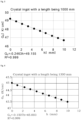
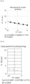
- an axial temperature gradient of the crystal ingot in periods of different growth stages in the region from the crystal growing solid-liquid interface to the first reference plane are plotted relative to the height of the solid-liquid interface.
- Fig. 1 in the initial period of the equal-d
- the fitting degree of all linear equations is greater than 0.998, indicating that the fitted linear equation is very in line with actual situations, according to the linear equation, the axial temperature gradient in the region from the solid-liquid interface to the first reference plane may be accurately controlled by adjusting the pulling speed and the gap, so as to effectively reduce the formation concentration of the point defects.
- the temperature gradient variation ⁇ G c in the axial direction at the central position of the crystal ingot is controlled to be 0.2 to 1 K/cm
- the temperature gradient variation ⁇ G e in the axial direction at an edge position of the crystal ingot is controlled to be 5 to 10 K/cm
- a radial temperature gradient G r of the crystal ingot is controlled to be not greater than 6 K/cm.
- the temperature gradient variation ⁇ G c in the axial direction of the central position is controlled to be 2 to 6 K/cm
- the temperature gradient variation ⁇ G e in the axial direction of the edge position is controlled to be 5 to 10 K/ cm
- the radial temperature gradient G r of the crystal ingot is controlled to be not greater than 10 K/cm.
- the temperature gradient variation ⁇ G c in the axial direction of the central position is controlled to be 0.2 to 1 K/cm
- the temperature gradient variation ⁇ G e in the axial direction of the edge position is controlled to be 5 to 10 K/cm
- the radial temperature gradient G r of the crystal ingot is controlled to be not greater than 6 K/cm.
- the method described in the present disclosure further includes adjusting a width of the temperature band from 1685K to 955K on the crystal ingot.
- the temperature band includes a first temperature band, a second temperature band, and a third temperature band.
- the first temperature band ranges from 1685K to 1605K.
- the second temperature band ranges from 1605K to 1355K.
- the third temperature band ranges from 1355K to 955K.
- the first temperature band includes temperature bands from 1685K to 1665K, 1665K to 1645K, 1645K to 1625K, and 1625K to 1605K.
- the first temperature band includes a several small temperature bands. The difference in the width of the small temperature bands is less than 1.0 mm, and the change in the width of the same temperature band during a growth process is less than 0.5 mm.
- the G 0 is a temperature gradient at the solid-liquid interface, with a value being 35 to 55 K/cm.
- the D x is the width of the temperature band, the unit is mm. It may be understood that, in the same period of the equal-diameter growth stage, by adjusting the width of the first temperature band according to the linear equation, the difference in the width of the small temperature bands in the first temperature band is less than 1.0 mm, that is to say, the width of the small temperature bands is similar. Meanwhile, in each period of the equal-diameter growth stage, the change in the width of each small temperature band is less than 0.5 mm, that is to say, a variation of the width of each small temperature band is small, such that the position of the width of the first temperature band on the crystal ingot can be accurately controlled.
- adjustment of the temperature gradient G 0 at the solid-liquid interface is realized by adjusting the height of the gas flow-guide cylinder from the solid-liquid interface, so as to adjust the D 1 .
- the height H of the gas flow-guide cylinder from the solid-liquid interface is increased by lowering a quartz crucible through rotation of the crucible shaft, and the quartz crucible is closer to the heater to reduce Go, and then the width D 1 of the temperature band increases.
- the height H of the gas flow-guide cylinder from the solid-liquid interface is decreased by raising the quartz crucible through rotation of the crucible shaft, and the quartz crucible is far away from the heater to increase the Go, and then the width D 1 of the temperature band decreases.
- adjustment of the temperature gradient Go at the solid-liquid interface is realized by adjusting the height H of the gas flow-guide cylinder from the solid-liquid interface, so as to adjust the D 2 .
- the height H of the gas flow-guide cylinder from the solid-liquid interface is increased by lowering the quartz crucible through rotation of the crucible shaft, so that the quartz crucible is closer to the heater to reduce the G 0 , and the width D 2 of the temperature band increases.
- the height H of the gas flow-guide cylinder from the solid-liquid interface is decreased by raising the quartz crucible through rotation of the crucible shaft, such that the quartz crucible is far away from the heater to increase the Go, and the width D 2 of the temperature band decreases.
- the width D 3 of the temperature band in the mid-period is between the width D 1 of the temperature band in the initial period and the width D 2 of the temperature band in the later period.
- the width D 3 of the temperature band in the mid-period is equal to the width D 1 of the temperature band in the initial period; and at a moment of transition from the mid-period to the later period, the width D 3 of the temperature band in the mid-period is equal to the width D 2 of the temperature band in the later period, and the width D 3 of the temperature band in the mid-period changes between the D 1 and the D 2 .
- the width of the first temperature band is timely adjusted by adjusting the height of the gas flow-guide cylinder from the solid-liquid interface, so that it is finally close to the theoretical value, and the temperature distribution of the crystal ingot is effectively controlled.
- the curve is plotted by taking the temperature gradient G 0 at the solid-liquid interface as the abscissa and taking the width D x of the temperature band as the ordinate.
- the temperature gradient G 0 at the solid-liquid interface is taken as the abscissa
- the width D x of the temperature band is taken as the ordinate.
- the temperature gradient G 0 at the solid-liquid interface is taken as the abscissa
- the width D x of the temperature band is taken as the ordinate.
- the temperature gradient Go at the solid-liquid interface is taken as the abscissa
- the width D x of the temperature band is taken as the ordinate.
- the fitting degrees of the linear equations of the each small temperature range in the first temperature band are all greater than 0.95 or more, indicating that the fitted linear equation is very consistent with actual situations. Therefore, according to the linear equation of the first temperature band, it is guided to adjust the height of the gas flow-guide cylinder from the solid-liquid interface, which can accurately adjust the width of the first temperature band, control the thermal history of the crystal ingot, suppress the growth of the point defects, and control the size of the defects, thereby increasing the yield of growing perfect crystals.
- the second temperature band includes temperature bands from 1605K to 1555K, 1555K to 1505K, 1505K to 1455K, 1455K to 1405K, and 1405K to 1355K.
- the second temperature band includes a plurality of small temperature bands. The difference in the width of the small temperature bands is less than 1.5 mm, and the change in the width of the same temperature band during a growth process is less than 1.0 mm.
- the G 0 is a temperature gradient at the solid-liquid interface, with a value being 35 to 55 K/cm.
- the D y is the width of the temperature band, the unit is mm. It may be understood that the width of the second temperature band is adjusted according to the linear equation, in the same period of the equal-diameter growth stage, the difference in the widths of the small temperature bands in the second temperature band is less than 1.5 mm, that is to say, the width of the small temperature bands is almost the same. Meanwhile, in each period of the equal-diameter growth stage, the change in the width of each small temperature band is less than 1.0 mm, that is to say, a variation of the width of each small temperature band is small, and the position of the width of the first temperature band on the crystal ingot may be accurately controlled.
- the width D 5 of the temperature band is reduced and is closer to the theoretical value.
- the width D 6 of the temperature band in the mid-period is between the width D 4 of the temperature band in the initial period and the width D 5 of the temperature band in the later period.
- the width D 6 of the temperature band in the mid-period is equal to the width D 4 of the temperature band in the initial period; and at the moment of transition from the mid-period to the later period, the width D 6 of the temperature band in the mid-period is equal to the width D 5 of the temperature band in the later period, and the width D 6 of the temperature band changes between the D 4 and the D 5 in the mid-period.
- the fitting degree of the linear equations of each small temperature range in the second temperature band is greater than 0.95, and will not be repeated here. Therefore, according to the linear equation of the second temperature band, it is guided to adjust the distance between the water-cooling jacket and the outer wall of the crystal ingot or the cooling water flow in the water-cooling jacket, which can accurately adjust the width of the second temperature band and control the thermal history and defect sizes of the crystal ingot, thereby improving the yield of growing perfect crystals.
- the width D 7 of the temperature band is increased, which is closer to the theoretical value.
- the width of the temperature band remains unchanged, and the width D 8 of the temperature band in the mid-period is equal to the width D 7 of the temperature band in the initial period.
- the width D 8 of the temperature band is equal to the width D 7 of the temperature band at the moment in the initial period at the moment from the initial period to the mid-period, and in the mid-period and later period of the stage, the width D 8 of the temperature band always maintains unchanged.
- the fitting degree of the linear equations of the third temperature band is greater than 0.95, and will not be repeated here. Therefore, according to the linear equation of the third temperature band, it is guided to adjust the cooling water flow in the water-cooling jacket, which can accurately adjust the width of the third temperature band, and control the thermal history and defect sizes of the crystal ingot, thereby improving the yield of growing perfect crystals.
- the boundary layer when the liquid phase changes to the solid phase and grows crystals, there is a boundary layer between the solid-liquid interface and molten liquid and the boundary layer has a transport effect on the interface.
- the crystal growing driving force and the temperature gradient of the solid-liquid interface are determined by temperature distribution of the boundary layer, referring to Fig. 13 for details. It may be understood that, the boundary layer is located in a region from the solid-liquid interface to a second reference plane (the second reference plane is an interface 10 mm below the solid-liquid interface).
- Voronkov's theory points out those interstitial type point defects (I-type point defects) and vacancy type point defects (V-type point defects) are formed near the crystal growing solid-liquid interface, and point defects undergo convective diffusion and recombination at the boundary layer. Therefore, for different thermal field conditions, the crystal growing pulling speed and a gap can be adjusted at same time to realize or optimize the thermal field structure of the boundary layer, and make the temperature gradient distribution of the boundary layer meet requirements for preparing perfect crystals.
- the inventors proposes that the temperature gradient in the region from the solid-liquid interface to the second reference plane is adjusted (the second reference plane is an interface 10 mm below the solid-liquid interface), while the temperature gradient in the region from the solid-liquid interface to the first reference plane is adjusted.
- a temperature gradient is adjusted to the G H in a region from the solid-liquid interface to a second reference plane.
- the second reference plane is an interface 10 mm below the solid-liquid interface.
- the temperature gradient is respectively optimized in the present disclosure.
- a pulling speed of the crystal ingot is adjusted to be v 1
- a gap is adjusted to be d 1 according to the G H1 and the G h1
- the gap d 1 is decreased to increase G 0
- the G H1 and the G h1 are close to the theoretical values, and at the same time, the pulling speed may be reduced within the range of the pulling speed v 1 , so that point defects formed in the crystal have some time to fully diffuse and recombine to reduce a formation concentration of point defects.
- the gap d 2 is increased to decrease G 0 , and the G H2 and the G h2 are close to the theoretical values, and at the same time, the pulling speed may be reduced within the range of the pulling speed v 2 , so that point defects formed in the crystal have some time to fully diffuse and recombine to reduce the formation concentration of point defects.
- the gap d 3 is decreased to increase G 0 , and the G h3 and the G H3 are close to the theoretical value, and at the same time, the pulling speed v 3 may be reduced within the range of the pulling speed, so that point defects formed in the crystal have some time to fully diffuse and recombine to reduce the formation concentration of point defects.
- I-type point defects and V-type point defects formed during the crystal growth process are fully diffused and recombined at the solid-liquid interface, so that a formation concentration of point defects is reduced, the size of microdefects is controlled, and the width of perfect crystal window is increased.
- the method is particularly suitable for the growth of large-diameter crystal ingots, and the yield of perfect crystals of the large-diameter crystal ingots may be improved as well.
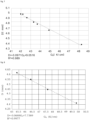
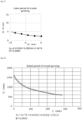
- an axial temperature gradient near the solid-liquid interface and a height relative to the solid-liquid interface are plotted at periods of different growth stages in the region from the solid-liquid interface to the second reference plane. As shown in Fig.
- the fitting degree of each of the above equations is greater than 0.99, indicating that the fitted equation is very consistent with the actual situation. Therefore, by correspondingly adjusting the pulling speed and the gap according to the equation, the axial temperature gradients in the region from the solid-liquid interface to the first reference plane and in the region from the solid-liquid interface to the second reference plane can effectively reduce the concentration of point defects.
- the value of the height H relative to the solid-liquid interface is negative, it means that it is located below the solid-liquid interface and its height from the interface is
- an temperature gradient variation ⁇ G c in the axial direction at a central position of the boundary layer is controlled to be 2 to 3 K/cm
- an temperature gradient variation ⁇ G e in the axial direction at an edge position of the boundary layer is controlled to be 3.5 to 5.5 K/cm
- the radial temperature gradient G r of the boundary layer is controlled to be not greater than 2 K/ cm.
- the temperature gradient variation ⁇ G c in the axial direction at the central position of the boundary layer is controlled to be 4 to 6 K/cm
- the temperature gradient variation ⁇ G e in the axial direction at the edge position of the boundary layer is controlled to be not greater than 5.4 K/cm
- the radial temperature gradient G r of the boundary layer is controlled to be not greater than 4 K/cm.
- the temperature gradient variation ⁇ G c in the axial direction at the central position of the boundary layer is controlled to be 2 to 3 K/ cm
- the temperature gradient variation ⁇ G e in the axial direction at the edge position of the boundary layer is controlled to be 3.5 to 5.5 K/cm
- the radial temperature gradient G r of the boundary layer is controlled to be not greater than 2 K/cm.
- the uniform temperature gradients distribution in the region below the solid-liquid interface ensures that the shape of the solid-liquid interface is close to a plane, which can improve the yield of perfect crystals, wherein the boundary layer is located in the region from the solid-liquid interface to the second reference plane.
- the area near the crystal ingot is the central area between a wall of the crystal ingot and an inner wall of the water-cooling jacket.
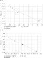
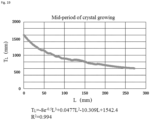
- the temperature of the area near the crystal ingot and a height relative to the solid-liquid interface are plotted at different crystal growing stages in the region from the crystal growing solid-liquid interface to the second reference plane.
- the fitting degree R 2 of the equation is 0.994.
- the fitting degree of each of the above equations is greater than 0.99, indicating that the fitted equation is very in line with actual situations. Therefore, according to the equation to adjust the gas flow rate near the crystal ingot is correspondingly adjusted, the temperature distribution of the area near the crystal ingot may be accurately controlled. This further affects the distribution of the temperature bands of the crystal ingot, further suppresses the size of microdefects, and improves the yield of perfect crystals.
- the present disclosure provides a silicon crystal.
- the silicon crystal is obtained through preparation by the above-mentioned method. Therefore, the silicon crystal has higher quality. It may be understood that, the proportion of windows belonging to perfect crystals in this silicon crystal is large.
- a temperature gradient G h in an area from a solid-liquid interface to a reference plane and the width of a temperature band of a crystal ingot are adjusted according to the following method, wherein a value of G 0 is 35 to 55 K/cm.
- the temperature gradient ⁇ G c in the axial direction of the central position of the crystal ingot is controlled to be 0.2 to 1 K/cm
- the temperature gradient ⁇ G e in the axial direction of the edge position of the crystal ingot is controlled to be 5 to 10 K/cm
- the radial temperature gradient G r of the crystal ingot is controlled to be not greater than 6 K/cm.
- the temperature gradient ⁇ G c in the axial direction of the central position of the crystal ingot is controlled to be 2 to 6 K/cm
- the temperature gradient ⁇ G e in the axial direction of the edge position of the crystal ingot is controlled to be 5 to 10 K/cm
- the radial temperature gradient G r of the crystal ingot is controlled to be not greater than 10 K/cm.
- the width D 3 of the temperature band is controlled to be between the width D 1 of the temperature band in the initial period and the width D 2 of the temperature band in a later period;
- the temperature range D 6 of a second temperature band from 1605K to 1355K is controlled to be between the width D 4 of the temperature band in the initial period and the width D 5 of the temperature band in the later period;
- the temperature range D z of a third temperature band from 1355K to 955K is controlled to maintain unchanged, and the width D 7 of the temperature band within the range of the third temperature band in the initial period of the equal-diameter growth stage is controlled to maintain unchanged.
- the temperature gradient ⁇ G c in the axial direction of the central position of the crystal ingot is controlled to be 0.2 to 1 K/cm
- the temperature gradient ⁇ G e in the axial direction of the edge position of the crystal ingot is controlled to be 5 to 10 K/cm
- the radial temperature gradient G r of the crystal ingot is controlled to be not greater than 6 K/cm.
- the width D 8 of the temperature band and the width D 7 of the temperature band within the range of the third temperature band in the initial period of the equal-diameter growth stage are controlled to maintain unchanged.
- a crystal ingot is pulled by using the existing growth apparatus and preparation method, i.e., compared with embodiment processes, the temperature gradient and the temperature band are not controlled.
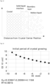
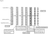
- the wafers at length of 180 mm, 340 mm, 650 mm, 950 mm, 1200 mm, and 1350 mm of the crystal ingot are respectively cut, defects of the wafers are characterized by the copper decoration method, and the defect characterization results are shown in Table 1, and the crystal ingots in the embodiments and the comparative embodiments are silicon crystal ingots. Referring to Fig.
- the specific operations characterized by the copper decoration method includes: firstly washing the test piece with tap water, then cleaning a surface of the test piece with a surfactant to remove surface particles on the surface of the test piece, then polishing and cleaning the surface of the test piece by means of chemical polishing, then coating copper nitrate on the surface of the cleaned test piece, forming copper precipitates on the surface of the test piece after heat treatment, followed by polishing and cleaning the surface of the test piece, and finally etching and developing.
- the copper precipitates generate compressive stresses in an area surrounding microdefects, these stresses are relieved by the release of silicon atoms, the released silicon atoms form new dislocations around the copper, and the copper precipitates are subsequently formed on these dislocations.
- the test piece is a silicon wafer. As many copper precipitates and dislocations form around the microdefects, forming a large area, the microdefects in the wafer may be observed under a microscope. The black portion of the micro-defect map is the perfect area and the white portion is the defect area.
- Table 1 displays the detection results of wafers at various positions of crystal ingot that are obtained from Embodiment 1 and Comparative embodiment 1 using copper decoration method. Wafer position (mm) Embodiment 1 Comparative embodiment 1 180 I-type defect V-type defect 340 Perfect crystal I-type defect 650 Perfect crystal I-type defect 950 Perfect crystal I-type defect 1200 Perfect crystal I-type defect 1350 I-type defect V-type defect
- Comparative embodiment 1 adopts the prior art method and the defects in the grown crystal ingot are V-type defects at first, I-type defects in the middle, and V-type defects at the end, and no perfect crystals appear in the entire crystal ingot.
- Embodiment 1 adopts the preparation method of the present disclosure and the grow crystal ingots have perfect crystals at the length of 340 mm, 650 mm, 950 mm, and 1200 mm and the windows are large (which can be directly seen from the copper decoration defect map), according to the V/G theory, within a certain range of pulling speed( 0.4 ⁇ v ⁇ 0.8 mm/min), there are perfect crystals in the range of length from 340 mm to 1200 mm. Therefore, the yield of the perfect crystals is improved indeed by adopting the preparation method of the present disclosure.
- a crystal ingot of 450 mm is grown, and in the area from the solid-liquid interface to the first reference plane and in the area from the solid-liquid interface to the second reference plane, temperature gradients G h and G H are adjusted by referring to the following equations, where a value of G 0 is 35-55 K/cm.
- a pulling speed of the crystal ingot is adjusted to be v 1
- a gap is adjusted to be d1 according to the G h1 and the G H1 , where the A 1 , B 1 , k 1 , v 1 , and d 1 meet: 0.03 ⁇ A 1 ⁇ 0.05, -0.3 ⁇ B 1 ⁇ -0.1, -0.12 ⁇ k 1 ⁇ -0.1, 0.4 ⁇ v 1 ⁇ 0.8 mm/min, and 50 ⁇ d 1 ⁇ 52 mm.
- the temperature gradient variation ⁇ G c in the axial direction of the central position of a boundary layer is controlled to be 2 to 3 K/ cm
- the temperature gradient variation ⁇ G e in the axial direction of the edge position of the boundary layer is controlled to be 3.5 to 5.5 K/cm
- the radial temperature gradient G r of the boundary layer is controlled to be not greater than 2 K/cm.
- the temperature gradient variation ⁇ G c in the axial direction of the central position in the area is controlled to be 0.2 to 1 K/cm
- the temperature gradient variation ⁇ G e in the axial direction of the edge position in the area is controlled to be 5 to 10 K/cm
- the radial temperature gradient G r in the area is controlled to be not greater than 6 K/cm.
- the temperature gradient variation ⁇ G c in the axial direction of the central position of the boundary layer is controlled to be 4 to 6 K/cm
- the temperature gradient variation ⁇ G e in the axial direction of the edge position of the boundary layer is controlled to be not greater than 5.4 K/cm
- the radial temperature gradient G r of the boundary layer is controlled to be not greater than 4 K/cm.
- the temperature gradient variation ⁇ G c in the axial direction of the central position in the area is controlled to be 2 to 6 K/cm
- the temperature gradient variation ⁇ G e in the axial direction of the edge position in the area is controlled to be 5 to 10 K/cm
- the radial temperature gradient G r in the area is controlled to be not greater than 10 K/cm.
- the temperature gradient variation ⁇ G c in the axial direction of the central position of the boundary layer is controlled to be 2 to 3 K/ cm
- the temperature gradient variation ⁇ G e in the axial direction of the edge position of the boundary layer is controlled to be 3.5 to 5.5 K/cm
- the radial temperature gradient G r of the boundary layer is controlled to be not greater than 2 K/cm.
- the temperature gradient variation ⁇ G c in the axial direction of the central position in the area is controlled to be 0.2 to 1 K/cm
- the temperature gradient variation ⁇ G e in the axial direction of the edge position in the area is controlled to be 5 to 10 K/cm
- the radial temperature gradient G r in the area is controlled to be not greater than 6 K/cm.
- a crystal ingot of 450 mm is pulled by using existing growth apparatus and the preparation method, i.e., compared with the process in Embodiment 2, the temperature gradient near the solid-liquid interface and the temperature near the crystal ingot are not controlled.
- the wafers at length of 100 mm, 400 mm, 700 mm, 1000 mm, and 1300 mm of the crystal ingot are respectively cut, the defects of the wafers are characterized by the copper decoration method, the defect characterization results are shown in Table 2, wherein the crystal ingots in the embodiments and the comparative embodiments are silicon crystal ingots.
- Table 2 displays the defect detection results of wafers at various positions of crystal ingot that are obtained from Embodiment 2 and Comparative embodiment 2 using the copper decoration method.
- Wafer position (mm) Embodiment 2 Comparative embodiment 2 100 I-type defect V-type defect 400 Perfect crystal I-type defect 700 Perfect crystal I-type defect 1000 Perfect crystal I-type defect 1300 Perfect crystal V-type defect
- Comparative embodiment 2 adopts the prior art method, and the defects in the grown crystal ingot are V-type defects at first, I-type defects in the middle, and V-type defects at last, and no perfect crystals appear in the entire crystal ingot.
- Embodiment 2 adopts the preparation method of the present disclosure, and the crystal ingots have perfect crystals at the length of 400 mm, 700 mm, 1000 mm, and 1300 mm, and the windows are large (which can be directly seen from the copper decoration defect map), according to the V/G theory, within a certain range of a pulling speed (0.4 ⁇ v ⁇ 0.8 mm/min), perfect crystals existed in the range of ingot length from 400 mm to 1300 mm. Therefore, the yield of the perfect crystals is improved indeed by adopting the preparation method of the present disclosure.
Landscapes
- Chemical & Material Sciences (AREA)
- Engineering & Computer Science (AREA)
- Crystallography & Structural Chemistry (AREA)
- Materials Engineering (AREA)
- Metallurgy (AREA)
- Organic Chemistry (AREA)
- Crystals, And After-Treatments Of Crystals (AREA)
Applications Claiming Priority (3)
| Application Number | Priority Date | Filing Date | Title |
|---|---|---|---|
| CN202111619103.2A CN114438585A (zh) | 2021-12-27 | 2021-12-27 | 单晶体的制备方法及硅晶体 |
| CN202111619092.8A CN114481302B (zh) | 2021-12-27 | 2021-12-27 | 单晶体的制备方法和硅晶体 |
| PCT/CN2022/140778 WO2023125206A1 (zh) | 2021-12-27 | 2022-12-21 | 单晶体的制备方法及硅晶体 |
Publications (2)
| Publication Number | Publication Date |
|---|---|
| EP4459013A1 true EP4459013A1 (de) | 2024-11-06 |
| EP4459013A4 EP4459013A4 (de) | 2026-03-18 |
Family
ID=86997755
Family Applications (1)
| Application Number | Title | Priority Date | Filing Date |
|---|---|---|---|
| EP22914460.5A Pending EP4459013A4 (de) | 2021-12-27 | 2022-12-21 | Verfahren zur herstellung eines einkristalls und siliciumkristall |
Country Status (3)
| Country | Link |
|---|---|
| EP (1) | EP4459013A4 (de) |
| TW (1) | TWI829486B (de) |
| WO (1) | WO2023125206A1 (de) |
Families Citing this family (2)
| Publication number | Priority date | Publication date | Assignee | Title |
|---|---|---|---|---|
| CN118639313B (zh) * | 2024-06-28 | 2025-06-10 | 宁夏中欣晶圆半导体科技有限公司 | 改善重掺砷d字条纹的拉晶方法 |
| CN119800490B (zh) * | 2025-03-13 | 2025-06-10 | 西安交通大学 | 导模法生长氧化镓晶体的模具设计方法、模具和生长炉 |
Family Cites Families (12)
| Publication number | Priority date | Publication date | Assignee | Title |
|---|---|---|---|---|
| US6254672B1 (en) * | 1997-04-09 | 2001-07-03 | Memc Electronic Materials, Inc. | Low defect density self-interstitial dominated silicon |
| JP4432458B2 (ja) * | 2003-10-30 | 2010-03-17 | 信越半導体株式会社 | 単結晶の製造方法 |
| JP5161492B2 (ja) * | 2007-05-31 | 2013-03-13 | Sumco Techxiv株式会社 | シリコン単結晶の製造方法 |
| CN103898597A (zh) * | 2012-12-25 | 2014-07-02 | 天津市硅酸盐研究所有限公司 | 一种导模法生长3"×9"大尺寸薄片状氧化铝单晶体的工艺方法 |
| WO2016019051A1 (en) * | 2014-07-31 | 2016-02-04 | Sunedison Semiconductor Limited | Nitrogen doped and vacancy dominated silicon ingot and thermally treated wafer formed therefrom having radially uniformly distributed oxygen precipitation density and size |
| CN112639175A (zh) * | 2018-08-23 | 2021-04-09 | 胜高股份有限公司 | 单晶硅的培育方法 |
| CN108914201B (zh) * | 2018-08-29 | 2019-09-27 | 西安理工大学 | 一种直拉硅单晶生长过程工艺参数优化方法 |
| CN110629283A (zh) * | 2019-09-23 | 2019-12-31 | 上海新昇半导体科技有限公司 | 一种硅单晶的生长方法 |
| CN112281210B (zh) * | 2020-10-10 | 2022-05-17 | 徐州鑫晶半导体科技有限公司 | 晶体的生长装置及生长方法 |
| CN113549997B (zh) * | 2021-06-25 | 2023-01-24 | 徐州鑫晶半导体科技有限公司 | 单晶生长的方法、装置及单晶体 |
| CN114438585A (zh) * | 2021-12-27 | 2022-05-06 | 徐州鑫晶半导体科技有限公司 | 单晶体的制备方法及硅晶体 |
| CN114481302B (zh) * | 2021-12-27 | 2023-10-24 | 中环领先(徐州)半导体材料有限公司 | 单晶体的制备方法和硅晶体 |
-
2022
- 2022-12-21 EP EP22914460.5A patent/EP4459013A4/de active Pending
- 2022-12-21 WO PCT/CN2022/140778 patent/WO2023125206A1/zh not_active Ceased
- 2022-12-26 TW TW111149973A patent/TWI829486B/zh active
Also Published As
| Publication number | Publication date |
|---|---|
| EP4459013A4 (de) | 2026-03-18 |
| TWI829486B (zh) | 2024-01-11 |
| WO2023125206A1 (zh) | 2023-07-06 |
| TW202328512A (zh) | 2023-07-16 |
Similar Documents
| Publication | Publication Date | Title |
|---|---|---|
| KR102095597B1 (ko) | 실리콘 단결정의 제조 방법 | |
| EP4459013A1 (de) | Verfahren zur herstellung eines einkristalls und siliciumkristall | |
| TW202014565A (zh) | 矽單結晶的成長方法 | |
| CN114606567A (zh) | n型单晶硅的制造方法、n型单晶硅的锭、硅晶片及外延硅晶片 | |
| JP2019206451A (ja) | シリコン単結晶の製造方法、エピタキシャルシリコンウェーハ及びシリコン単結晶基板 | |
| JP2001151596A (ja) | エピタキシャル成長用シリコンウエーハ及びエピタキシャルウエーハ並びにその製造方法 | |
| JP4853237B2 (ja) | エピタキシャルウェーハの製造方法 | |
| TW202113168A (zh) | 一種矽單晶的生長方法 | |
| JP3867476B2 (ja) | シリコン単結晶の製造方法及びシリコン単結晶の製造装置 | |
| CN114481302B (zh) | 单晶体的制备方法和硅晶体 | |
| JP4151474B2 (ja) | 単結晶の製造方法及び単結晶 | |
| JP3719088B2 (ja) | 単結晶育成方法 | |
| JP4231275B2 (ja) | シリコンウェーハの製造方法およびその製造装置およびシリコンウェーハ | |
| CN104334774A (zh) | 单晶硅晶锭和晶片以及用于生长所述晶锭的装置和方法 | |
| CN114438585A (zh) | 单晶体的制备方法及硅晶体 | |
| JP2007182373A (ja) | 高品質シリコン単結晶の製造方法及びこれを用いて製造されたシリコン単結晶ウェーハ | |
| KR101384060B1 (ko) | 실리콘 단결정 잉곳 성장 방법 | |
| JP5375636B2 (ja) | シリコン単結晶の製造方法 | |
| JP4080657B2 (ja) | シリコン単結晶インゴットの製造方法 | |
| KR100846632B1 (ko) | 실리콘 단결정의 제조방법, 그리고 그 방법으로 제조된실리콘 단결정 잉곳 및 웨이퍼 | |
| JP6459944B2 (ja) | シリコン単結晶の製造方法 | |
| JP4016471B2 (ja) | 結晶育成方法 | |
| JP4200690B2 (ja) | GaAsウェハの製造方法 | |
| KR101366154B1 (ko) | 반도체용 고품질 실리콘 단결정 잉곳 및 웨이퍼 | |
| TWI701363B (zh) | 矽單晶長晶方法 |
Legal Events
| Date | Code | Title | Description |
|---|---|---|---|
| STAA | Information on the status of an ep patent application or granted ep patent |
Free format text: STATUS: THE INTERNATIONAL PUBLICATION HAS BEEN MADE |
|
| PUAI | Public reference made under article 153(3) epc to a published international application that has entered the european phase |
Free format text: ORIGINAL CODE: 0009012 |
|
| STAA | Information on the status of an ep patent application or granted ep patent |
Free format text: STATUS: REQUEST FOR EXAMINATION WAS MADE |
|
| 17P | Request for examination filed |
Effective date: 20240725 |
|
| AK | Designated contracting states |
Kind code of ref document: A1 Designated state(s): AL AT BE BG CH CY CZ DE DK EE ES FI FR GB GR HR HU IE IS IT LI LT LU LV MC ME MK MT NL NO PL PT RO RS SE SI SK SM TR |
|
| DAV | Request for validation of the european patent (deleted) | ||
| DAX | Request for extension of the european patent (deleted) | ||
| A4 | Supplementary search report drawn up and despatched |
Effective date: 20260213 |
|
| RIC1 | Information provided on ipc code assigned before grant |
Ipc: C30B 29/06 20060101AFI20260209BHEP Ipc: C30B 15/20 20060101ALI20260209BHEP Ipc: C30B 15/14 20060101ALI20260209BHEP Ipc: C30B 15/22 20060101ALI20260209BHEP |