EP4458546A2 - Anzeigemodul und verfahren zum formen eines anzeigemoduls - Google Patents
Anzeigemodul und verfahren zum formen eines anzeigemoduls Download PDFInfo
- Publication number
- EP4458546A2 EP4458546A2 EP24200098.2A EP24200098A EP4458546A2 EP 4458546 A2 EP4458546 A2 EP 4458546A2 EP 24200098 A EP24200098 A EP 24200098A EP 4458546 A2 EP4458546 A2 EP 4458546A2
- Authority
- EP
- European Patent Office
- Prior art keywords
- die
- display module
- coating material
- leds
- molding
- Prior art date
- Legal status (The legal status is an assumption and is not a legal conclusion. Google has not performed a legal analysis and makes no representation as to the accuracy of the status listed.)
- Granted
Links
Images








Classifications
-
- B—PERFORMING OPERATIONS; TRANSPORTING
- B29—WORKING OF PLASTICS; WORKING OF SUBSTANCES IN A PLASTIC STATE IN GENERAL
- B29C—SHAPING OR JOINING OF PLASTICS; SHAPING OF MATERIAL IN A PLASTIC STATE, NOT OTHERWISE PROVIDED FOR; AFTER-TREATMENT OF THE SHAPED PRODUCTS, e.g. REPAIRING
- B29C45/00—Injection moulding, i.e. forcing the required volume of moulding material through a nozzle into a closed mould; Apparatus therefor
- B29C45/17—Component parts, details or accessories; Auxiliary operations
- B29C45/26—Moulds
- B29C45/33—Moulds having transversely, e.g. radially, movable mould parts
-
- H—ELECTRICITY
- H10—SEMICONDUCTOR DEVICES; ELECTRIC SOLID-STATE DEVICES NOT OTHERWISE PROVIDED FOR
- H10H—INORGANIC LIGHT-EMITTING SEMICONDUCTOR DEVICES HAVING POTENTIAL BARRIERS
- H10H20/00—Individual inorganic light-emitting semiconductor devices having potential barriers, e.g. light-emitting diodes [LED]
- H10H20/80—Constructional details
- H10H20/85—Packages
- H10H20/852—Encapsulations
- H10H20/853—Encapsulations characterised by their shape
-
- B—PERFORMING OPERATIONS; TRANSPORTING
- B29—WORKING OF PLASTICS; WORKING OF SUBSTANCES IN A PLASTIC STATE IN GENERAL
- B29C—SHAPING OR JOINING OF PLASTICS; SHAPING OF MATERIAL IN A PLASTIC STATE, NOT OTHERWISE PROVIDED FOR; AFTER-TREATMENT OF THE SHAPED PRODUCTS, e.g. REPAIRING
- B29C45/00—Injection moulding, i.e. forcing the required volume of moulding material through a nozzle into a closed mould; Apparatus therefor
- B29C45/14—Injection moulding, i.e. forcing the required volume of moulding material through a nozzle into a closed mould; Apparatus therefor incorporating preformed parts or layers, e.g. injection moulding around inserts or for coating articles
- B29C45/14065—Positioning or centering articles in the mould
-
- B—PERFORMING OPERATIONS; TRANSPORTING
- B29—WORKING OF PLASTICS; WORKING OF SUBSTANCES IN A PLASTIC STATE IN GENERAL
- B29C—SHAPING OR JOINING OF PLASTICS; SHAPING OF MATERIAL IN A PLASTIC STATE, NOT OTHERWISE PROVIDED FOR; AFTER-TREATMENT OF THE SHAPED PRODUCTS, e.g. REPAIRING
- B29C45/00—Injection moulding, i.e. forcing the required volume of moulding material through a nozzle into a closed mould; Apparatus therefor
- B29C45/14—Injection moulding, i.e. forcing the required volume of moulding material through a nozzle into a closed mould; Apparatus therefor incorporating preformed parts or layers, e.g. injection moulding around inserts or for coating articles
- B29C45/14311—Injection moulding, i.e. forcing the required volume of moulding material through a nozzle into a closed mould; Apparatus therefor incorporating preformed parts or layers, e.g. injection moulding around inserts or for coating articles using means for bonding the coating to the articles
-
- B—PERFORMING OPERATIONS; TRANSPORTING
- B29—WORKING OF PLASTICS; WORKING OF SUBSTANCES IN A PLASTIC STATE IN GENERAL
- B29C—SHAPING OR JOINING OF PLASTICS; SHAPING OF MATERIAL IN A PLASTIC STATE, NOT OTHERWISE PROVIDED FOR; AFTER-TREATMENT OF THE SHAPED PRODUCTS, e.g. REPAIRING
- B29C45/00—Injection moulding, i.e. forcing the required volume of moulding material through a nozzle into a closed mould; Apparatus therefor
- B29C45/16—Making multilayered or multicoloured articles
- B29C45/1671—Making multilayered or multicoloured articles with an insert
-
- H—ELECTRICITY
- H10—SEMICONDUCTOR DEVICES; ELECTRIC SOLID-STATE DEVICES NOT OTHERWISE PROVIDED FOR
- H10H—INORGANIC LIGHT-EMITTING SEMICONDUCTOR DEVICES HAVING POTENTIAL BARRIERS
- H10H20/00—Individual inorganic light-emitting semiconductor devices having potential barriers, e.g. light-emitting diodes [LED]
- H10H20/01—Manufacture or treatment
-
- H—ELECTRICITY
- H10—SEMICONDUCTOR DEVICES; ELECTRIC SOLID-STATE DEVICES NOT OTHERWISE PROVIDED FOR
- H10W—GENERIC PACKAGES, INTERCONNECTIONS, CONNECTORS OR OTHER CONSTRUCTIONAL DETAILS OF DEVICES COVERED BY CLASS H10
- H10W90/00—Package configurations
-
- B—PERFORMING OPERATIONS; TRANSPORTING
- B29—WORKING OF PLASTICS; WORKING OF SUBSTANCES IN A PLASTIC STATE IN GENERAL
- B29C—SHAPING OR JOINING OF PLASTICS; SHAPING OF MATERIAL IN A PLASTIC STATE, NOT OTHERWISE PROVIDED FOR; AFTER-TREATMENT OF THE SHAPED PRODUCTS, e.g. REPAIRING
- B29C45/00—Injection moulding, i.e. forcing the required volume of moulding material through a nozzle into a closed mould; Apparatus therefor
- B29C45/14—Injection moulding, i.e. forcing the required volume of moulding material through a nozzle into a closed mould; Apparatus therefor incorporating preformed parts or layers, e.g. injection moulding around inserts or for coating articles
- B29C45/14065—Positioning or centering articles in the mould
- B29C2045/14131—Positioning or centering articles in the mould using positioning or centering means forming part of the insert
-
- B—PERFORMING OPERATIONS; TRANSPORTING
- B29—WORKING OF PLASTICS; WORKING OF SUBSTANCES IN A PLASTIC STATE IN GENERAL
- B29C—SHAPING OR JOINING OF PLASTICS; SHAPING OF MATERIAL IN A PLASTIC STATE, NOT OTHERWISE PROVIDED FOR; AFTER-TREATMENT OF THE SHAPED PRODUCTS, e.g. REPAIRING
- B29C45/00—Injection moulding, i.e. forcing the required volume of moulding material through a nozzle into a closed mould; Apparatus therefor
- B29C45/14—Injection moulding, i.e. forcing the required volume of moulding material through a nozzle into a closed mould; Apparatus therefor incorporating preformed parts or layers, e.g. injection moulding around inserts or for coating articles
- B29C45/14311—Injection moulding, i.e. forcing the required volume of moulding material through a nozzle into a closed mould; Apparatus therefor incorporating preformed parts or layers, e.g. injection moulding around inserts or for coating articles using means for bonding the coating to the articles
- B29C2045/14319—Injection moulding, i.e. forcing the required volume of moulding material through a nozzle into a closed mould; Apparatus therefor incorporating preformed parts or layers, e.g. injection moulding around inserts or for coating articles using means for bonding the coating to the articles bonding by a fusion bond
-
- B—PERFORMING OPERATIONS; TRANSPORTING
- B29—WORKING OF PLASTICS; WORKING OF SUBSTANCES IN A PLASTIC STATE IN GENERAL
- B29K—INDEXING SCHEME ASSOCIATED WITH SUBCLASSES B29B, B29C OR B29D, RELATING TO MOULDING MATERIALS OR TO MATERIALS FOR MOULDS, REINFORCEMENTS, FILLERS OR PREFORMED PARTS, e.g. INSERTS
- B29K2995/00—Properties of moulding materials, reinforcements, fillers, preformed parts or moulds
- B29K2995/0018—Properties of moulding materials, reinforcements, fillers, preformed parts or moulds having particular optical properties, e.g. fluorescent or phosphorescent
- B29K2995/0026—Transparent
-
- B—PERFORMING OPERATIONS; TRANSPORTING
- B29—WORKING OF PLASTICS; WORKING OF SUBSTANCES IN A PLASTIC STATE IN GENERAL
- B29L—INDEXING SCHEME ASSOCIATED WITH SUBCLASS B29C, RELATING TO PARTICULAR ARTICLES
- B29L2031/00—Other particular articles
- B29L2031/34—Electrical apparatus, e.g. sparking plugs or parts thereof
- B29L2031/3475—Displays, monitors, TV-sets, computer screens
-
- H—ELECTRICITY
- H10—SEMICONDUCTOR DEVICES; ELECTRIC SOLID-STATE DEVICES NOT OTHERWISE PROVIDED FOR
- H10H—INORGANIC LIGHT-EMITTING SEMICONDUCTOR DEVICES HAVING POTENTIAL BARRIERS
- H10H20/00—Individual inorganic light-emitting semiconductor devices having potential barriers, e.g. light-emitting diodes [LED]
- H10H20/01—Manufacture or treatment
- H10H20/036—Manufacture or treatment of packages
- H10H20/0362—Manufacture or treatment of packages of encapsulations
Definitions
- Embodiments of the disclosure relate to a display module with improved manufacturing efficiency and contrast ratio and a method for molding a display module.
- LED displays constitute a display screen using a plurality of display modules disposed with a plurality of LEDs, and is widely used in indoor and outdoor large scale billboards and large scale electronic display board markets. Further, LED displays may be implemented as high quality large scale screens with superior brightness and color compared to previous LCD displays.
- the LED displays are disadvantageous in that durability is decreased as a result of damage being generated by damage from the environment (e.g., moisture, ultraviolet rays, etc.) of being exposed outside or damage from static generated from a hand or body of a user in the process of installation
- damage from the environment e.g., moisture, ultraviolet rays, etc.
- a coating solution for waterproofing each of the plurality of LEDs disposed on the LED display has been conventionally applied through a dispensing or spraying method.
- a method for molding a display module includes: forming a cavity using a die plate of a first die and a plurality of side surface dies; filling the cavity with a coating material; fixing the display module to a second die using a coupling body disposed on a second surface of the display module, opposite of a first surface of the display module disposed with a plurality of LEDs; soaking the display module in the coating material filled in the cavity; curing the coating material; and separating the cured coating material of the display module from the die plate.
- the method further includes cooling the coating material after curing the coating material.
- the forming the cavity includes moving the plurality of side surface dies to contact the die plate.
- the filling the cavity with the coating material includes injecting the coating material such that a height of the coating material is greater than a height of the plurality of LEDs disposed on the first surface.
- the separating the cured coating material from the die plate includes separating the plurality of side surface dies from the die plate.
- each of the plurality of side surface dies includes: a contact body configured to contact with the die plate; an actuator including an axis coupled with the contact body, the actuator configured to move the contact body; and a guide body provided on the first die and configured to guide the contact body by slidably-coupling with the contact body, wherein the contact body is configured to slidably move along the guide body.
- the soaking the display module in the coating material includes soaking the display module in a direction of the first surface such that a side surface of the plurality of LEDs is covered with the coating material.
- the coating material includes a heat-curable resin having a light-transmissivity.
- the die plate includes a plurality of grooves formed in a shape corresponding to the plurality of LEDs at a position corresponding to the plurality of LEDs, and the soaking the display module in the coating material includes inserting the plurality of LEDs into the plurality of grooves, respectively.
- the coating material includes: a first coating material filled in the plurality of grooves and having a first light transmittance; and a second coating material stacked on the first coating material, and having a second light transmittance lower than the first light transmittance.
- a display module includes a substrate comprising: a first surface disposed with a plurality of LEDs; a second surface, opposite of the first surface, that is disposed with a plurality of chips connected to the plurality of LEDs and further disposed with a coupling body.
- the display module further includes a molding part covering the first surface and the plurality of LEDs, and having a shape corresponding to a shape of the plurality of LEDs.
- the molding part includes: a first portion formed to surround the plurality of LEDs; and a second portion positioned on an upper part of the first surface that is not disposed with the plurality of LEDs, wherein the first portion and the second portion are formed integrally.
- a thickness of the first portion is smaller than a thickness of the second portion.
- a first light transmittance of the first portion is higher than a second light transmittance of the second portion.
- the molding part includes a heat-curable resin having a light-transmissivity.
- a method for forming a display module includes soaking a first surface of a substrate in a coating material, the first surface disposed with a plurality of LEDs, and the substrate further including a second surface, opposite of the first surface, that is disposed with a plurality of chips connected to the plurality of LEDs and further disposed with a coupling body; and curing the coating material while the first surface of the substrate is soaked in the coating material, the cured coating material forming a molding part that covers the first surface and the plurality of LEDs, and has a shape corresponding to a shape of the plurality of LEDs.
- the molding part includes: a first portion formed to surround the plurality of LEDs; and a second portion positioned on an upper part of the first surface that is not disposed with the plurality of LEDs, wherein the first portion and the second portion are formed integrally.
- a thickness of the first portion is smaller than a thickness of the second portion.
- a first light transmittance of the first portion is higher than a second light transmittance of the second portion.
- the coating material includes a heat-curable resin having a light-transmissivity
- the curing the coating material includes heat curing the coating material
- first first
- second second
- first first
- second second
- Embodiments of the disclosure may relate to providing a method for molding a display module with improved manufacturing efficiency and contrast ratio.
- a structure of a molding device 1 according to an embodiment may be described below with references to FIGS. 1 to 8 .
- FIG. 1 is a perspective diagram illustrating a molding device 1 according to an embodiment of the disclosure
- FIG. 2 is an exploded perspective diagram illustrating a molding device 1 according to an embodiment of the disclosure
- FIG. 3A is a cross-sectional diagram taken long line A-A of FIG. 1
- FIG. 3B is an enlarged diagram illustrating area B of FIG. 3A
- FIG. 4 is a lower perspective diagram illustrating a second die 20 according to an embodiment of the disclosure
- FIG. 5 is a lower exploded perspective diagram illustrating a second die 20 according to an embodiment of the disclosure
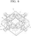
- FIG. 6 is a perspective diagram illustrating a first die 10 according to an embodiment of the disclosure
- FIG. 7 is an enlarged diagram illustrating area D of FIG. 6
- FIG. 8 is an exploded perspective diagram illustrating a first side surface die 30-1 according to an embodiment of the disclosure.
- the molding device 1 may be a device molding a display module disposed with a plurality of LEDs, and may include a first die 10 and a second die 20 coupled to be detachable from the first die 10.
- the die may be designating a press mold for manufacturing, and may be designated as a molding, a mold, a core, or an injection molding.
- the first die 10 may be coupled with the second die 20 for molding the display module 40, and may include a die plate 11 for forming an exterior of a molding part 60 (see FIG. 3B ) of the display module 40, a plurality of side surface dies 30 capable of selectively contacting with the die plate 11, a heating line 70 (see FIG. 11 ) capable of applying heat to the die plate 11, and a cooling line 80 (see FIG. 11 ) capable of cooling the die plate 11.
- the die plate 11 may form a cavity C to be filled with a coating material T for molding a display module 40 together with the plurality of side surface dies 30.
- the cavity C which is a space that the coating material T may be injected, may be formed.
- the shape of display module 40 may be determined according to the die plate 11 and the shape of the plurality of side surface dies 30 contacting the die plate 11.
- the shape of a front surface of the die plate 11 may correspond with the shape of an upper surface 61 of the molding part 60
- the shape of the plurality of side surface dies 30 may correspond with the shape of a side surface 62 of the molding part 60.
- the upper surface 61 of the molding part 60 may be formed flatly, and in case the die plate 11 has a shape of an uneven part, the uneven part may be formed on the upper surface of the molding part 60.
- a size of the die plate 11 may correspond with a size of a substrate 41. Accordingly, even when the display module 40 formed with the molding part 60 on the substrate 41 is completed, a process of removing a separate molding part to fit the size of the substrate 41 may not be needed.
- the first die 10 may include a first die contact surface 12 capable of contacting with a second die contact surface 22 of the second die 20.
- the first die contact surface 12 may have a shape complementing the second die contact surface 22.
- an inner space of a molding device 1 including the die plate 11 may be sealed from the outside.
- the inner space of the molding device 1 may refer to a space including the cavity C containing the coating material T.
- the inner space of the molding device 1 may be vacuumed when the first die 10 and the second die 20 are in contact.
- the first die contact surface 12 may be formed with a sealing or a sealing groove 13 for inserting an O-ring. Accordingly, when the first die 10 and the second die 20 are in contact, the inner space of the molding device 1 may be completely sealed from the outside.
- the plurality of side surface dies 30 may be provided on the first die 10, and provided to selectively contact the side surfaces of the die plate 11.
- the specific structure of the plurality of side surface dies 30 may be described hereafter with reference to FIG. 8 .
- the display module 40 may include a first surface 41-1 disposed with a plurality of LEDs P, a plurality of chips 100 to be opposite to the first surface 41-1 and electrically connected with the plurality of LEDs P, and a substrate 41 including a second surface 41-2 disposed with a coupling member 48.
- the coupling member 48 may include at least one coupling body.
- the plurality of LEDs P may be, as self-light emitting display elements, inorganic light emitting elements that emits light on its own, and disposed at a pre-set distance on the substrate 41.
- the plurality of LEDs P may operate as one pixel, and the one pixel may include a red light emitting diode (LED) emitting a red light, a green LED emitting green light, and a blue LED emitting a blue light.
- the one pixel may further include a white LED in addition to the red (R)/green (G)/ blue (B) LED.
- one pixel may realize various colors through the combination of red LED, green LED, and blue LED.
- the plurality of LEDs of one display module has been described above as constituting one pixel, the plurality of LEDs may constitute a plurality of pixels in the embodiment.
- the first surface 41-1 disposed with the plurality of LEDs P may be disposed to face the die plate 11 of the first die 10.
- the plurality of chips 100 may be disposed on the second surface 41-2 of the substrate 41, and may control the plurality of LEDs P.
- the plurality of chips 100 may include various semiconductor chips such as a processor and a transistor, and provide a control signal and/or power to the plurality of LEDs P through wiring formed on the substrate 41.
- the coupling member 48 may be disposed on the second surface 41-2 of the substrate 41.
- the coupling member 48 may be configured in plurality, and disposed uniformly (or dispersingly) at a peripheral area of the substrate 41 to stably fix the display module 40 to the second die 20.
- the coupling member 48 may be composed of a metal, and disposed to protrude from the second surface 41-2. Accordingly, because the coupling member 48 may be coupled to the second die 20, the display module 40 may be stably fixed to the second die 20.
- the display module 40 may be conveniently detachable from the second die 20, and the molding efficiency of the display module 40 may be improved.
- the coupling member 48 may fix the display module 40 to the second die 20 when molding the display module 40, and the display module 40 with the molding completed may be fixed to a tiling plate (not shown).
- the coupling member 48 may be used for fixing the molding of the display module 40, and fixing to constitute a display screen, the manufacturing efficiency of a display device using the display module 40 may be improved.
- the second die 20 may be positioned on the upper part of the first die 10, and may move vertically relative to the first die 10.
- the second die 20 may include the second die contact surface 22 contacting the first die contact surface 12 of the first die 10, a first sealing member 23 sealing the inner space of the molding device 1 by contacting with the plurality of side surface dies 30, and a fixing member 26 for fixing the display module 40.
- the first sealing member 23 may include at least one sealing body
- the fixing member 26 may include at least one fixing body.
- the first sealing member 23 may be disposed around the fixing member 26, and may seal the inner space of the molding device 1 by contacting with a contact member 31 of the plurality of side surface dies 30 installed in the first die 10 (see FIG. 11 ).
- the contact member 31 may include at least one contact body.
- the first sealing member 23 may be composed of rubber with elastic force, and fixed to the second die 20.
- the fixing member 26 may be configured to fix the display module 40, and may be inserted in the second die 20.
- the fixing member 26 may include a coupling hole 24 to which the coupling member 48 may be inserted, a receiving hole 25 formed in the shape of the plurality of chips 100, and a magnetic material 28 for fixing the coupling member 48.
- the coupling hole 24 may correspond to the number of the coupling member 48, and may be formed at a position corresponding to a position where the coupling member 48 is protrudingly disposed. Accordingly, when the coupling member 48 is inserted into the coupling hole 24, the coupling member 48 may be fixed into the coupling hole 24 by the magnetic material 28 disposed adjacently to the coupling hole 24.
- the molding efficiency of the display module 40 may be improved.
- the coupling member 48 may be fitted-coupled to the coupling hole 24, or thread-coupled.
- the receiving hole 25, as a space for containing the plurality of chips 100, may be a shape corresponding to the position and shape of the pre-set plurality of chips 100.
- the fixing member 26 receives pressure, the plurality of chips 100 inserted into the receiving hole 25 may be prevented from becoming damaged.
- the shape of the receiving hole 25 may be varied, and the fixing member 26 may also be changed according to the display module 40 for molding.
- the plurality of side surface dies 30 may be configured in plurality.
- the plurality of side surface dies 30 may include a first side surface die to a fourth side surface die 30-1, 30-2, 30-3 and 30-4.
- FIG. 8 is described based on the first side surface die 30-1, but the configuration of the first side surface die 30-1 is the same as the configurations of the second side surface to the fourth side surface die 30-2, 30-3 and 30-4.
- the first side surface die 30-1 may include the contact member 31 contacting the die plate 11, and an actuator 35 axis-coupled with the contact member 31 and may move the contact member 31.
- the contact member 31 may be in selective contact with the side surfaces of the die plate 11 to form cavity C together with the die plate 11.
- the contact member 31 may include a second sealing member 32 directly contacting the die plate 11, and a connecting member 33 connecting the second sealing member 32 with an axis 34 of the actuator 35.
- the second sealing member 32 may form the cavity C together with the die plate 11, and may seal a side surface of the cavity so that the coating material T filling the cavity C does not leak.
- the second sealing member 32 may be formed of a rubber with elastic force.
- the second sealing member 31 may include at least one sealing body.
- a first contact surface 32a of the second sealing member 32 and a second contact surface 33a of the connecting member 33 may form one flat surface.
- first contact surface 32a and the second contact surface 33a may contact the die plate 11 to form the cavity C and simultaneously seal the side surface of the cavity C so that the coating material T filling the cavity C does not leak.
- the connecting member 33 may include a seating part 33b that seats and fixes the second sealing member 32, a coupling groove 33c that receives and fixes the axis 34, and a guide slot 33d that guides the movement of the contact member 31 and is formed on both side surfaces.
- the coupling groove 33c may be configured to a shape for the actuator 35 to insert and fix one end of the axis 34, and may move the contact member 31 along the movement of the axis 34.
- the guide slot 33d may receive a guide protruding part 52a of the guide member 50 as illustrated in FIG. 7 , and move along the guide protruding part 52a.
- the guide member 50 may include at least one guide body.
- the contact member 31 may not be inclined toward one side and may be guided to have stable movement by connection with the guide member 50.
- the guide member 50 may be provided on the first die 10 and may be slidably-coupled with the contact member 31 to guide the contact member 31. Specifically, a respective one of the guide member 50 may be disposed on each of the both sides of the side surface dies 30 and may guide the side surface dies 30.
- the guide protruding part 52a may be formed on one side of the guide member 50, and the guide protruding part 52a may be inserted into the guide slot 33d of the contact member 31 and the contact member 31 may be moved.
- the actuator 35 may have a configuration for controlling power to the first side surface die 30, and may be formed in various configurations such as a motor.
- the actuator 35 may be disposed on each of the side surfaces of the first die 10.
- a coupling surface 35a of the actuator 35 may be fixed to the side surface of the first die 10.
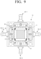
- FIG. 9 is an upper surface diagram illustrating a state in which a die plate 11 and a plurality of side surface dies 30 are spaced apart according to an embodiment of the disclosure
- FIG. 10 is an upper surface diagram illustrating a state in which a die plate 11 and a plurality of side surface dies 30 are in contact according to an embodiment of the disclosure.
- a first side surface die to a fourth side surface die 30-1, 30-2, 30-3, and 30-4 may be in a first state of being spaced apart at predetermined intervals with the die plate 11.
- the contact member of each of the first side surface die to the fourth side surface die 30-1, 30-2, 30-3, and 30-4 may be in a state of being spaced apart with the die plate 11. That is, the cavity C may not be in a formed state in the first state.
- the first side surface die to the fourth side surface die 30-1, 30-2, 30-3, and 30-4 may be moved to be in contact with the die plate 11.
- the actuator 35 of each of the first side surface die to the fourth side surface die 30-1, 30-2, 30-3, and 30-4 may move the contact member 31 through the axis 34. Accordingly, the contact member 31 may contact the die plate 11 by being guided by the guide member 50.
- the first side surface die to the fourth side surface die 30-1, 30-2, 30-3, and 30-4 may be in a second state of being in contact with the die plate 11.
- the contact member 31 and the die plate 11 may then form the cavity C, which is a space for the coating material T to be filled.
- the cavity C may be formed as the plurality of side surface dies 30 are moved to contact the die plate 11.
- the cavity C may refer to a rectangular parallelepiped space due to the shape of the contact member 31 and the die plate 11.
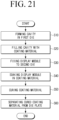
- a method for molding a display module 40 according to an embodiment may be described in greater detail below with references to FIGS. 11 to 15 and 21 .
- FIG. 11 is a cross-sectional diagram illustrating a state in which a die plate 11 and a plurality of side surface dies 30 form a cavity C according to an embodiment of the disclosure
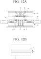
- FIG. 12A is a cross-sectional diagram illustrating a state in which a cavity C is filled with coating material T according to an embodiment of the disclosure
- FIG. 12B is an enlarged diagram illustrating area E of FIG. 12A
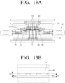
- FIG. 13A is a cross-sectional diagram illustrating a state in which a first die 10 and a second die 20 are coupled according to an embodiment of the disclosure
- FIG. 13B is an enlarged diagram illustrating area F of FIG. 13A
- FIG. 14 is a cross-sectional diagram illustrating a state in which a plurality of side surface dies 30 has moved in the state illustrated in FIG. 13A
- FIG. 15 is a cross-sectional diagram illustrating a state in which a first die 10 and a second die 20 are spaced apart according to an embodiment of the disclosure
- FIG. 21 is a flowchart illustrating a method for molding a display module 40 according to an embodiment of the disclosure.
- the cavity C may be formed using the die plate 11 of the first die 10 and the plurality of side surface dies 30 (S10).
- the contact member 31 of the plurality of side surface dies 30 may contact the side surface of the die plate 11 to form the cavity C, which is a space in which the coating material T may be injected.
- the coating material T may be filled in the formed cavity C (S20).
- the coating material T may include a heat-curable resin having a light-transmissivity. Accordingly, the coating material T may be in a state of having a predetermined viscosity at room temperature, and when heat is applied to the coating material T, the coating material T may be cured.
- the coating material may include a binder resin, a photopolymerization initiator, a black pigment and a solvent, or may be comprised of a resin composition including black pigment for shielding.
- the coating material T constitutes the plurality of LEDs P and the molding part 60 that covers the substrate disposed with the plurality of LEDs P, the outside light introduced to the display module 40 may be absorbed while simultaneously improving contrast ratio, and by protecting the plurality of LEDs P, the plurality of LEDs P may be prevented from being damaged by moisture, static, and the like.
- the coating material T may be formed to a first height H1 on the die plate 11.
- the first height H1 may be higher than a second height H2 of the plurality of LEDs P covering all of the upper surface and the side surfaces of the plurality of LEDs P.
- the coating material T may be injected to be higher than the height of the plurality of LEDs P disposed on the first surface 41-1 of the display module 40.
- the display module 40 may be fixed to the second die 20 (S30).
- the display module 40 may be in a state in which the plurality of LEDs P is disposed on the first surface 41-1 of the substrate 41, and the plurality of chips 100 is disposed on the second surface 41-2.
- the display module 40 may be fixed to the second die 20 through the coupling member 48 disposed on the second surface 41-2 opposite to the first surface 41-1 disposed with the plurality of LEDs P.
- the display module 40 may be fixed to the second die 20.
- the plurality of chips 100 is inserted into the receiving hole 25 which is formed to the shape of the plurality of chips 100 on the fixing member 26, damage to the plurality of chips 100 may be prevented even when being downward pressed as the second die 20 and the first die 10 are in contact.
- the display module 40 may then be soaked in the coating material T (S40).
- the second die 20 may, when the display module 40 is in a fixed state, be moved to be in contact with the first die 10.
- the second die 20 may be moved until the coating material T filled in the cavity C covers all of the first surface 41-1 and the plurality of LEDs P. That is, the first surface 41-1 may contact the coating material T until the side surfaces of the plurality of LEDs P are covered.
- the second die 20 may move toward the first die 10 so that a sum of the second height H2 of the plurality of LEDs P and the third height H3 of the coating material T on the plurality of LEDs P is the same as the first height H1 at which the coating material T is in contact with the first surface 41-1.
- the cavity C may be sealed from the outside, and when a vacuum line (not shown) is formed on the molding device 1, the inside may become vacuumed.
- the coating material T may be cured as the display module 40 is in a soaked state in the coating material T (S50). Specifically, the coating material T may receive heat from a heating line 70 provided in the first die 10 thereby rising in temperature, and the heat-curable coating material T may be cured.
- the heating line 70 may be sufficient if provided on the first die 10 to apply heat to the coating material T, and the method of heating may be varied.
- the heating line 70 may not be limited to being formed on the first die 10, but may also be formed on the second die 20.
- the coating material T may be cured when the plurality of LEDs P and the first surface 41-1 of the display module 40 is covered and may form the molding part 60.
- the molding part 60 that is cured may then be cooled through a cooling line 80 provided in the second die 20 thereby lowering in temperature. That is, after the coating material T is cured, the coating material T may be cooled.
- the cooling line 80 may be sufficient if provided on the first die 10 to cool the molding part 60, and the method of cooling may be varied.
- cooling line 80 may not be limited to being formed on the first die 10, but may also be formed on the second die 20.
- the heating line 70 and the cooling line 80 may be formed with the same line, and the heating or cooling may be selectively performed according to the temperature of the fluid flowing in the corresponding line.
- the coating material T of the display module 40 that is cured may be separated from the die plate 11 (S60).
- the plurality of side surface dies 30 may be spaced apart from the die plate 11. Specifically, the contact member 31 of the plurality of side surface dies 30 may be spaced apart from the side surface 62 of the molding part 60.
- the second die 20 may move relative to the first die 10, and the molding part 60 may be separated from the die plate 11. Specifically, the upper surface 61 of the molding part 60 may be separated from the die plate 11.
- the molding part 60 may be separated from the die plate 11 and the plurality of side surface dies 30.
- the molding part 60 by forming the molding part 60 through the mold method, time required for forming the molding part 60 may be significantly reduced, and since the coating material T is a quantitative amount filling the cavity C, the amount of coating material T may also be reduced, thereby improving the manufacturing efficiency of the display module 40 significantly.
- a structure of the display module 40 constructed through the method for molding the display module illustrated in FIGS. 11 to 15 may be described below.
- FIG. 16 is a cross-sectional diagram illustrating a display module 40 according to an embodiment of the disclosure.
- the display module 40 may cover the first surface 41-1 and the plurality of LEDs P, and may include the molding part 60 with the shape corresponding to the shape of the plurality of LEDs P.
- the upper surface of the molding part 60 may be formed flatly. Accordingly, as the light emitted from the plurality of LEDs P is not refracted by the molding part 60, a uniform brightness of the display screen may be realized.
- the molding part may be composed of a material that absorbs outside light, and by absorbing the outside light, the contrast ratio of the display screen may be improved.
- the molding part 60 that is cured and covers the plurality of LEDs P and the first surface 41-1 on the substrate 41 disposed with the plurality of LEDs P, the plurality of LEDs P may be protected from outside moisture, static and the like, and the lifespan of the display module 40 may be improved.
- a molding device 1' and a display module 40' manufactured by the molding device 1' according to a modified embodiment may be described below with references to FIGS. 17A to 18 .
- FIG. 17A is a cross-sectional view illustrating a molding device 1' according to a modified embodiment of the disclosure
- FIG. 17B is an enlarged diagram illustrating area G of FIG. 17A
- FIG. 18 is a cross-sectional diagram illustrating a display module 40' according to a modified embodiment of the disclosure.
- first die 10 the second die 20
- the plurality of side surface dies 30, and the fixing member 26 are the same as described above, and overlapping descriptions have been omitted.
- the die plate 11' may include a plurality of grooves 14-1 formed to a shape corresponding to the plurality of LEDs P at the position corresponding to the plurality of LEDs P. Accordingly, the operation of soaking a display module 40' in the coating material T may further include an operation of inserting the plurality of LEDs P respectively into the plurality of grooves 14-1.
- the die plate 11' may include the plurality of grooves 14-1 and a protruding part 14-2 formed between the plurality of grooves.
- a molding part 60' with a first portion 60'-1 and a second portion 60'-2 may be formed by the plurality of grooves 14-1 and the protruding part 14-2.
- the molding part 60' may include a first portion 60'-1 protrudingly formed to surround the plurality of LEDs P and a second portion 60'-2 positioned on the upper part of the first surface 41-1 not disposed with the plurality of LEDs P.
- the first portion 60'-1 may be formed by the plurality of grooves 14-1, and the second portion 60'-2 may be formed by the protruding part 14-2. That is, the first portion 60'-1 and the second portion 60'-2 may be a shape complementary to the die plate 11' including the plurality of grooves 14-1 and the protruding part 14-2.
- first portion 60'-1 and the second portion 60'-2 may be formed integrally with the same material.
- the shape of the plurality of grooves 14-1 may be a rectangular parallelepiped shape. That is the die plate 11' may include a surface with a uneven part pattern, which is the rectangular parallelepiped shape.
- a first display module 40'-1 and a second display module 40'-2 including the molding part 60' formed by the die plate 11' including the plurality of grooves 14-1 and the protruding part 14-2 may be disposed side by side.
- the gap in the first portion 60'-1 may include a pre-set spacing distance L.
- the spacing distance L may correspond with the widthwise length of the protruding part 14-2.
- the distance between the gap of the first portion 60'-1 disposed on the edge of the second display module 40'-2 adjacent with the first portion 60'-1 disposed on the edge of a first display module 40'-1 may be the same as the pre-set spacing distance L.
- the distance of the gaps of the first portion 60'-1 may all satisfy the pre-set spacing distances L.
- the molding part 60' absorbs outside light by being composed of a material that absorbs outside light, a seamless screen configured by the plurality of display modules may be realized.
- the first portion 60'-1 and the second portion 60'-2 may be composed of materials different from each other. Specifically, a first light transmittance of the first portion 60'-1 may be higher than a second light transmittance of the second portion 60'-2.
- the coating material T may be filled in the plurality of grooves 14-1, and may include a first coating material with the first light transmittance and a second coating material stacked on the first coating material with the second light transmittance, which is lower than the first light transmittance.
- the first coating material with the first light transmittance may be first injected in the plurality of grooves 14-1, and by stacking the second coating material with the second light transmittance on the upper part of the first coating material, the coating material T may be formed.
- the first light transmittance of the first portion 60'-1 may then be higher than the second light transmittance of the second portion 60'-2 through the method for molding the display module according to FIGS. 11 to 15 .
- the coating material T including the black pigment may absorb outside light better the lower the light transmittance.
- the first portion 60'-1 surrounding the plurality of LEDs P may realize a display screen without loss of light emitting from the plurality of LEDs P due to the first portion 60'-1 with high light transmittance.
- the gap of the plurality of LEDs P may be configured to not be visible externally.
- the plurality of display modules may be arranged to implement a large scale display screen, a predetermined brightness or more of the plurality of LEDs P concurrently with a seamless display may be realized.
- a molding device 1" and a display module 40" manufactured by the molding device 1" according to another modified embodiment will be described below.
- FIG. 19A is a cross-sectional diagram illustrating a molding device 1" according to another modified embodiment of the disclosure
- FIG. 19B is an enlarged diagram illustrating area H of FIG. 19A
- FIG. 20 is a cross-sectional diagram illustrating a display module 60" according to another modified embodiment of the disclosure.
- first die 10 the second die 20
- the plurality of side surface dies 30, and the fixing member 26 are the same as described above, and overlapping descriptions have been omitted.
- a thickness of a first portion 60"-1 may be smaller than a thickness of a second portion 60"-2 on a die plate 11".
- a sixth height H6 corresponding to the thickness of the first portion 60"-1 may be smaller than a seventh height H7 corresponding to the thickness of the second portion 60"-2.
- the sixth height H6 may refer to the length from the upper surface of the plurality of LEDs P to an upper surface 11"-3 of the plurality of grooves
- the seventh height H7 may refer to the length from the first surface 41-1 of the substrate 41 to an upper surface 11"-2 of the protruding part.
- the sixth height H6 may be smaller than a fifth height H5 of the first portion 60'-1 illustrated in FIGS. 17B to 18
- the seventh height H7 may be smaller than an eighth height H8 of the second portion 60'-2 illustrated in FIGS. 17B to 18 .
- the sixth height H6 of the first portion 60"-1 is smaller than the eighth height H8 of the second portion 60"-2, the light transmittance of the first portion 60"-1 may be better than the light transmittance of the second portion 60"-2, and an outside light absorption rate of the first portion 60"-1 may be smaller than an outside light absorption rate of the second portion 60"-2.
- the first portion 60"-1 surrounding the plurality of LEDs P may realize a display screen without loss of light emitting from the plurality of LEDs P due to the first portion 60"-1 with high light transmittance.
- the gap of the plurality of LEDs P may be configured to not be visible externally.
- the plurality of display modules may be arranged to implement a large scale display screen, a predetermined brightness or more of the plurality of LEDs P concurrently with a seamless display may be realized.
- an exchange of the faulty LED may also be performed through the molding method.
- the corresponding LED and the molding part 60 adjacent to the LED may be removed.
- the method for removing the molding part 60 such as physical removal method and chemical removal method may be varied according to necessity.
- a new LED may then be disposed on the substrate 41 to the position corresponding to the faulty LED.
- the disposing the new LED on the substrate 41 may include connecting the gap between the new LED and the substrate 41 electrically and physically.
- a coating material is filled into an empty space of the molding part 60, that is removed, adjacent to the corresponding LED, and the corresponding portion may be cured by pressing and heating through a die.
- a unit molding part of one unit adjacent to one LED may be manufactured in plurality through the molding method, and the corresponding manufactured unit molding part may be inserted and fixed in the empty space of the molding part 60, that is removed, adjacent to the corresponding LED.
- the unit molding part may be a shape corresponding to the first portion 60-1 surrounding to one LED.
- the invention might include, relate to, and / or be defined by, the following aspects:
Landscapes
- Engineering & Computer Science (AREA)
- Manufacturing & Machinery (AREA)
- Mechanical Engineering (AREA)
- Led Device Packages (AREA)
- Devices For Indicating Variable Information By Combining Individual Elements (AREA)
- Injection Moulding Of Plastics Or The Like (AREA)
- Physics & Mathematics (AREA)
- General Physics & Mathematics (AREA)
- Theoretical Computer Science (AREA)
- Casting Or Compression Moulding Of Plastics Or The Like (AREA)
Applications Claiming Priority (2)
| Application Number | Priority Date | Filing Date | Title |
|---|---|---|---|
| KR1020190053619A KR102579748B1 (ko) | 2019-05-08 | 2019-05-08 | 디스플레이 모듈 및 디스플레이 모듈 몰딩 방법 |
| EP20173256.7A EP3736102B1 (de) | 2019-05-08 | 2020-05-06 | Anzeigemodul und verfahren zum formen eines anzeigemoduls |
Related Parent Applications (2)
| Application Number | Title | Priority Date | Filing Date |
|---|---|---|---|
| EP20173256.7A Division EP3736102B1 (de) | 2019-05-08 | 2020-05-06 | Anzeigemodul und verfahren zum formen eines anzeigemoduls |
| EP20173256.7A Division-Into EP3736102B1 (de) | 2019-05-08 | 2020-05-06 | Anzeigemodul und verfahren zum formen eines anzeigemoduls |
Publications (3)
| Publication Number | Publication Date |
|---|---|
| EP4458546A2 true EP4458546A2 (de) | 2024-11-06 |
| EP4458546A3 EP4458546A3 (de) | 2025-01-01 |
| EP4458546B1 EP4458546B1 (de) | 2025-11-19 |
Family
ID=70613646
Family Applications (3)
| Application Number | Title | Priority Date | Filing Date |
|---|---|---|---|
| EP20173256.7A Active EP3736102B1 (de) | 2019-05-08 | 2020-05-06 | Anzeigemodul und verfahren zum formen eines anzeigemoduls |
| EP24200095.8A Active EP4454854B1 (de) | 2019-05-08 | 2020-05-06 | Anzeigemodul |
| EP24200098.2A Active EP4458546B1 (de) | 2019-05-08 | 2020-05-06 | Anzeigemodul |
Family Applications Before (2)
| Application Number | Title | Priority Date | Filing Date |
|---|---|---|---|
| EP20173256.7A Active EP3736102B1 (de) | 2019-05-08 | 2020-05-06 | Anzeigemodul und verfahren zum formen eines anzeigemoduls |
| EP24200095.8A Active EP4454854B1 (de) | 2019-05-08 | 2020-05-06 | Anzeigemodul |
Country Status (4)
| Country | Link |
|---|---|
| US (2) | US11527687B2 (de) |
| EP (3) | EP3736102B1 (de) |
| KR (1) | KR102579748B1 (de) |
| WO (1) | WO2020226422A1 (de) |
Families Citing this family (1)
| Publication number | Priority date | Publication date | Assignee | Title |
|---|---|---|---|---|
| CN113763832B (zh) * | 2021-09-17 | 2024-01-30 | 利亚德光电股份有限公司 | Led显示模组的制备方法 |
Family Cites Families (22)
| Publication number | Priority date | Publication date | Assignee | Title |
|---|---|---|---|---|
| KR100621154B1 (ko) * | 2005-08-26 | 2006-09-07 | 서울반도체 주식회사 | 발광 다이오드 제조방법 |
| KR100789951B1 (ko) * | 2006-06-09 | 2008-01-03 | 엘지전자 주식회사 | 발광 유닛 제작 장치 및 방법 |
| KR20090115340A (ko) * | 2008-05-02 | 2009-11-05 | 오명수 | 발광다이오드 모듈 및 발광다이오드 모듈의 패키징장치 및발광다이오드 모듈 |
| TWI573185B (zh) * | 2009-05-12 | 2017-03-01 | 美國伊利諾大學理事會 | 用於可變形及半透明顯示器之超薄微刻度無機發光二極體之印刷總成 |
| KR101122136B1 (ko) | 2011-07-12 | 2012-03-16 | 신한다이아몬드공업 주식회사 | 압축 몰딩식 봉지재 성형장치 |
| CN102737554A (zh) * | 2012-06-29 | 2012-10-17 | 北京金立翔艺彩科技股份有限公司 | 一种支撑基板的制造方法及led显示装置 |
| KR101945202B1 (ko) | 2012-08-14 | 2019-02-08 | 삼성디스플레이 주식회사 | 유기 전계 표시 장치 |
| US9532464B2 (en) * | 2013-07-22 | 2016-12-27 | Rohm Co., Ltd. | LED lighting apparatus |
| JP6459354B2 (ja) | 2014-09-30 | 2019-01-30 | 日亜化学工業株式会社 | 透光部材及びその製造方法ならびに発光装置及びその製造方法 |
| KR20160053750A (ko) * | 2014-10-29 | 2016-05-13 | 삼성에스디아이 주식회사 | 디스플레이 밀봉재용 조성물, 이를 포함하는 유기보호층, 및 이를 포함하는 디스플레이 장치 |
| JP6356581B2 (ja) * | 2014-11-19 | 2018-07-11 | 信越化学工業株式会社 | 半導体装置の製造方法 |
| JP6570305B2 (ja) | 2015-05-12 | 2019-09-04 | 三菱電機株式会社 | 表示装置 |
| KR102262895B1 (ko) * | 2015-05-28 | 2021-06-09 | 삼성전자주식회사 | 디스플레이 모듈 및 이를 구비한 디스플레이 장치 |
| KR102396332B1 (ko) * | 2015-09-22 | 2022-05-12 | 삼성전자주식회사 | Led 디스플레이용 미세간격 코팅부재 및 이를 이용한 코팅방법 |
| KR20170055787A (ko) | 2015-11-12 | 2017-05-22 | 삼성전자주식회사 | 반도체 패키지 제조용 몰딩 장치 및 이를 이용한 반도체 패키지의 몰딩 방법 |
| KR102486308B1 (ko) | 2016-06-10 | 2023-01-10 | 삼성전자주식회사 | 디스플레이 모듈 및 이에 대한 코팅방법 |
| JP6790899B2 (ja) * | 2017-02-17 | 2020-11-25 | 日亜化学工業株式会社 | 発光モジュールの製造方法及び発光モジュール |
| KR101829190B1 (ko) | 2017-02-22 | 2018-02-14 | 엑센도 주식회사 | 글래스 외주면이 몰딩된 지문센서 패키지의 제조방법 |
| KR102017014B1 (ko) | 2017-05-22 | 2019-09-03 | 주식회사 엘지화학 | 다층 점착 테이프 |
| KR102504223B1 (ko) | 2017-11-10 | 2023-02-28 | 현대자동차주식회사 | 대용량 데이터를 포함하는 이미지 혹은 영상을 차량 내 헤드업 디스플레이 장치에 표시하는 방법 및 장치 |
| JP7053532B2 (ja) * | 2019-06-07 | 2022-04-12 | 株式会社ニフコ | ディスプレイ装置及びその製造方法並びにディスプレイ装置を備えるインストルメントパネル |
| US12218286B2 (en) * | 2020-11-12 | 2025-02-04 | Seoul Semiconductor Co., Ltd. | Light emitting module and method of manufacturing the same and display apparatus having the same |
-
2019
- 2019-05-08 KR KR1020190053619A patent/KR102579748B1/ko active Active
-
2020
- 2020-05-06 EP EP20173256.7A patent/EP3736102B1/de active Active
- 2020-05-06 EP EP24200095.8A patent/EP4454854B1/de active Active
- 2020-05-06 EP EP24200098.2A patent/EP4458546B1/de active Active
- 2020-05-07 WO PCT/KR2020/005973 patent/WO2020226422A1/en not_active Ceased
- 2020-05-08 US US16/869,719 patent/US11527687B2/en active Active
-
2022
- 2022-11-07 US US17/982,229 patent/US11978836B2/en active Active
Also Published As
| Publication number | Publication date |
|---|---|
| US20200357963A1 (en) | 2020-11-12 |
| EP4454854A3 (de) | 2024-12-25 |
| US11978836B2 (en) | 2024-05-07 |
| US20230054995A1 (en) | 2023-02-23 |
| EP4454854B1 (de) | 2025-11-19 |
| KR102579748B1 (ko) | 2023-09-19 |
| EP3736102A1 (de) | 2020-11-11 |
| EP4458546A3 (de) | 2025-01-01 |
| KR20200129349A (ko) | 2020-11-18 |
| EP4458546B1 (de) | 2025-11-19 |
| EP4454854A2 (de) | 2024-10-30 |
| WO2020226422A1 (en) | 2020-11-12 |
| US11527687B2 (en) | 2022-12-13 |
| EP3736102B1 (de) | 2024-11-06 |
Similar Documents
| Publication | Publication Date | Title |
|---|---|---|
| US10700047B2 (en) | Panel with a notch accommodating a component, display apparatus including the same, and method of manufacturing the same | |
| CN113053860A (zh) | 显示模块以及具有该显示模块的显示装置 | |
| KR20140140491A (ko) | 표시장치 및 그 제조 방법 | |
| JP2014195083A (ja) | 発光素子パッケージモジュール | |
| US10241357B2 (en) | Mould frame and liquid crystal display module having thereof | |
| TW202016622A (zh) | 顯示模組、包括其的顯示裝置以及製造顯示模組的方法 | |
| US20110187957A1 (en) | Display device and method for manufacturing the same | |
| EP4454854B1 (de) | Anzeigemodul | |
| KR20210075820A (ko) | 디스플레이 모듈을 포함하는 디스플레이 장치 및 그 제조 방법 | |
| CN113376892A (zh) | 背光单元和包括该背光单元的显示装置 | |
| US10477696B2 (en) | Fine interval coating member for LED display and coating method using the same | |
| EP4401159A1 (de) | Anzeigevorrichtung mit anzeigemodul und herstellungsverfahren dafür | |
| US20210063807A1 (en) | Display apparatus | |
| KR102275727B1 (ko) | 평판표시장치모듈 | |
| KR20220091278A (ko) | 디스플레이 모듈을 포함하는 디스플레이 장치 및 그 제조 방법 | |
| KR102743014B1 (ko) | 디스플레이 장치 | |
| EP4358164A1 (de) | Anzeigevorrichtung mit anzeigemodul und herstellungsverfahren dafür | |
| CN112599029B (zh) | 一种led显示屏的制备方法 | |
| US20150253616A1 (en) | Display apparatus | |
| KR101950828B1 (ko) | 액정표시장치 | |
| KR20230092313A (ko) | 디스플레이 모듈을 포함하는 디스플레이 장치 및 그 제조 방법 | |
| KR101593653B1 (ko) | 발광 모듈 및 발광 모듈 제조방법 | |
| KR101949387B1 (ko) | 엘이디패키지 및 그 제조방법과 엘이디패키지를 포함하는 액정표시장치 | |
| KR20230128935A (ko) | 디스플레이 모듈을 포함하는 디스플레이 장치 및 그 제조 방법 | |
| KR102603594B1 (ko) | 유기 발광 표시 장치 |
Legal Events
| Date | Code | Title | Description |
|---|---|---|---|
| PUAI | Public reference made under article 153(3) epc to a published international application that has entered the european phase |
Free format text: ORIGINAL CODE: 0009012 |
|
| STAA | Information on the status of an ep patent application or granted ep patent |
Free format text: STATUS: THE APPLICATION HAS BEEN PUBLISHED |
|
| AC | Divisional application: reference to earlier application |
Ref document number: 3736102 Country of ref document: EP Kind code of ref document: P |
|
| AK | Designated contracting states |
Kind code of ref document: A2 Designated state(s): AL AT BE BG CH CY CZ DE DK EE ES FI FR GB GR HR HU IE IS IT LI LT LU LV MC MK MT NL NO PL PT RO RS SE SI SK SM TR |
|
| REG | Reference to a national code |
Ref country code: DE Free format text: PREVIOUS MAIN CLASS: B29C0045140000 Ref country code: DE Ref legal event code: R079 Ref document number: 602020062642 Country of ref document: DE Free format text: PREVIOUS MAIN CLASS: B29C0045140000 Ipc: B29C0045330000 |
|
| PUAL | Search report despatched |
Free format text: ORIGINAL CODE: 0009013 |
|
| AK | Designated contracting states |
Kind code of ref document: A3 Designated state(s): AL AT BE BG CH CY CZ DE DK EE ES FI FR GB GR HR HU IE IS IT LI LT LU LV MC MK MT NL NO PL PT RO RS SE SI SK SM TR |
|
| RIC1 | Information provided on ipc code assigned before grant |
Ipc: B29L 31/34 20060101ALN20241125BHEP Ipc: H01L 33/58 20100101ALI20241125BHEP Ipc: H01L 33/56 20100101ALI20241125BHEP Ipc: H01L 33/54 20100101ALI20241125BHEP Ipc: H01L 25/16 20230101ALI20241125BHEP Ipc: H01L 25/075 20060101ALI20241125BHEP Ipc: B29C 45/14 20060101ALI20241125BHEP Ipc: B29C 45/33 20060101AFI20241125BHEP |
|
| STAA | Information on the status of an ep patent application or granted ep patent |
Free format text: STATUS: REQUEST FOR EXAMINATION WAS MADE |
|
| 17P | Request for examination filed |
Effective date: 20250325 |
|
| GRAP | Despatch of communication of intention to grant a patent |
Free format text: ORIGINAL CODE: EPIDOSNIGR1 |
|
| STAA | Information on the status of an ep patent application or granted ep patent |
Free format text: STATUS: GRANT OF PATENT IS INTENDED |
|
| RIC1 | Information provided on ipc code assigned before grant |
Ipc: B29C 45/33 20060101AFI20250901BHEP Ipc: B29C 45/14 20060101ALI20250901BHEP Ipc: H01L 25/075 20060101ALI20250901BHEP Ipc: H01L 25/16 20230101ALI20250901BHEP Ipc: H10H 20/01 20250101ALI20250901BHEP Ipc: H10H 20/853 20250101ALI20250901BHEP Ipc: B29L 31/34 20060101ALN20250901BHEP |
|
| INTG | Intention to grant announced |
Effective date: 20250910 |
|
| GRAS | Grant fee paid |
Free format text: ORIGINAL CODE: EPIDOSNIGR3 |
|
| GRAA | (expected) grant |
Free format text: ORIGINAL CODE: 0009210 |
|
| STAA | Information on the status of an ep patent application or granted ep patent |
Free format text: STATUS: THE PATENT HAS BEEN GRANTED |
|
| AC | Divisional application: reference to earlier application |
Ref document number: 3736102 Country of ref document: EP Kind code of ref document: P |
|
| AK | Designated contracting states |
Kind code of ref document: B1 Designated state(s): AL AT BE BG CH CY CZ DE DK EE ES FI FR GB GR HR HU IE IS IT LI LT LU LV MC MK MT NL NO PL PT RO RS SE SI SK SM TR |
|
| REG | Reference to a national code |
Ref country code: CH Ref legal event code: F10 Free format text: ST27 STATUS EVENT CODE: U-0-0-F10-F00 (AS PROVIDED BY THE NATIONAL OFFICE) Effective date: 20251119 Ref country code: GB Ref legal event code: FG4D |
|
| REG | Reference to a national code |
Ref country code: DE Ref legal event code: R096 Ref document number: 602020062642 Country of ref document: DE |
|
| REG | Reference to a national code |
Ref country code: IE Ref legal event code: FG4D |
|
| REG | Reference to a national code |
Ref country code: NL Ref legal event code: MP Effective date: 20251119 |
|
| PGFP | Annual fee paid to national office [announced via postgrant information from national office to epo] |
Ref country code: GB Payment date: 20260324 Year of fee payment: 7 |
|
| PG25 | Lapsed in a contracting state [announced via postgrant information from national office to epo] |
Ref country code: ES Free format text: LAPSE BECAUSE OF FAILURE TO SUBMIT A TRANSLATION OF THE DESCRIPTION OR TO PAY THE FEE WITHIN THE PRESCRIBED TIME-LIMIT Effective date: 20251119 |
|
| REG | Reference to a national code |
Ref country code: LT Ref legal event code: MG9D |
|
| PG25 | Lapsed in a contracting state [announced via postgrant information from national office to epo] |
Ref country code: NO Free format text: LAPSE BECAUSE OF FAILURE TO SUBMIT A TRANSLATION OF THE DESCRIPTION OR TO PAY THE FEE WITHIN THE PRESCRIBED TIME-LIMIT Effective date: 20260219 |
|
| PG25 | Lapsed in a contracting state [announced via postgrant information from national office to epo] |
Ref country code: AT Free format text: LAPSE BECAUSE OF FAILURE TO SUBMIT A TRANSLATION OF THE DESCRIPTION OR TO PAY THE FEE WITHIN THE PRESCRIBED TIME-LIMIT Effective date: 20251119 Ref country code: HR Free format text: LAPSE BECAUSE OF FAILURE TO SUBMIT A TRANSLATION OF THE DESCRIPTION OR TO PAY THE FEE WITHIN THE PRESCRIBED TIME-LIMIT Effective date: 20251119 Ref country code: FI Free format text: LAPSE BECAUSE OF FAILURE TO SUBMIT A TRANSLATION OF THE DESCRIPTION OR TO PAY THE FEE WITHIN THE PRESCRIBED TIME-LIMIT Effective date: 20251119 |
|
| REG | Reference to a national code |
Ref country code: AT Ref legal event code: MK05 Ref document number: 1858487 Country of ref document: AT Kind code of ref document: T Effective date: 20251119 |
|
| PG25 | Lapsed in a contracting state [announced via postgrant information from national office to epo] |
Ref country code: NL Free format text: LAPSE BECAUSE OF FAILURE TO SUBMIT A TRANSLATION OF THE DESCRIPTION OR TO PAY THE FEE WITHIN THE PRESCRIBED TIME-LIMIT Effective date: 20251119 |
|
| PG25 | Lapsed in a contracting state [announced via postgrant information from national office to epo] |
Ref country code: RS Free format text: LAPSE BECAUSE OF FAILURE TO SUBMIT A TRANSLATION OF THE DESCRIPTION OR TO PAY THE FEE WITHIN THE PRESCRIBED TIME-LIMIT Effective date: 20260219 |
|
| PG25 | Lapsed in a contracting state [announced via postgrant information from national office to epo] |
Ref country code: IS Free format text: LAPSE BECAUSE OF FAILURE TO SUBMIT A TRANSLATION OF THE DESCRIPTION OR TO PAY THE FEE WITHIN THE PRESCRIBED TIME-LIMIT Effective date: 20260319 |
|
| PG25 | Lapsed in a contracting state [announced via postgrant information from national office to epo] |
Ref country code: PT Free format text: LAPSE BECAUSE OF FAILURE TO SUBMIT A TRANSLATION OF THE DESCRIPTION OR TO PAY THE FEE WITHIN THE PRESCRIBED TIME-LIMIT Effective date: 20260319 |
|
| PG25 | Lapsed in a contracting state [announced via postgrant information from national office to epo] |
Ref country code: PL Free format text: LAPSE BECAUSE OF FAILURE TO SUBMIT A TRANSLATION OF THE DESCRIPTION OR TO PAY THE FEE WITHIN THE PRESCRIBED TIME-LIMIT Effective date: 20251119 |
|
| PG25 | Lapsed in a contracting state [announced via postgrant information from national office to epo] |
Ref country code: LV Free format text: LAPSE BECAUSE OF FAILURE TO SUBMIT A TRANSLATION OF THE DESCRIPTION OR TO PAY THE FEE WITHIN THE PRESCRIBED TIME-LIMIT Effective date: 20251119 |