EP4362066A1 - Manufacturing method of semiconductor element, semiconductor layer support structure, and semiconductor substrate - Google Patents
Manufacturing method of semiconductor element, semiconductor layer support structure, and semiconductor substrate Download PDFInfo
- Publication number
- EP4362066A1 EP4362066A1 EP23189698.6A EP23189698A EP4362066A1 EP 4362066 A1 EP4362066 A1 EP 4362066A1 EP 23189698 A EP23189698 A EP 23189698A EP 4362066 A1 EP4362066 A1 EP 4362066A1
- Authority
- EP
- European Patent Office
- Prior art keywords
- polishing
- semiconductor
- semiconductor layer
- semiconductor layers
- layer
- Prior art date
- Legal status (The legal status is an assumption and is not a legal conclusion. Google has not performed a legal analysis and makes no representation as to the accuracy of the status listed.)
- Pending
Links
- 239000004065 semiconductor Substances 0.000 title claims abstract description 444
- 239000000758 substrate Substances 0.000 title claims abstract description 178
- 238000004519 manufacturing process Methods 0.000 title claims abstract description 54
- 238000005498 polishing Methods 0.000 claims abstract description 131
- 239000000853 adhesive Substances 0.000 claims abstract description 113
- 230000001070 adhesive effect Effects 0.000 claims abstract description 113
- 229910052594 sapphire Inorganic materials 0.000 claims abstract description 68
- 239000010980 sapphire Substances 0.000 claims abstract description 68
- 238000005304 joining Methods 0.000 claims abstract description 22
- 230000014759 maintenance of location Effects 0.000 claims abstract description 17
- 230000001678 irradiating effect Effects 0.000 claims abstract description 4
- 238000000034 method Methods 0.000 claims description 121
- 238000007517 polishing process Methods 0.000 claims description 28
- 230000003746 surface roughness Effects 0.000 claims description 5
- 239000010410 layer Substances 0.000 description 362
- 239000011521 glass Substances 0.000 description 40
- 239000010409 thin film Substances 0.000 description 29
- XUIMIQQOPSSXEZ-UHFFFAOYSA-N Silicon Chemical compound [Si] XUIMIQQOPSSXEZ-UHFFFAOYSA-N 0.000 description 28
- 229910052710 silicon Inorganic materials 0.000 description 28
- 239000010703 silicon Substances 0.000 description 28
- 239000012790 adhesive layer Substances 0.000 description 23
- 239000000463 material Substances 0.000 description 9
- 230000000694 effects Effects 0.000 description 8
- 238000010586 diagram Methods 0.000 description 6
- 230000003287 optical effect Effects 0.000 description 6
- 239000002002 slurry Substances 0.000 description 6
- 229910002601 GaN Inorganic materials 0.000 description 5
- JMASRVWKEDWRBT-UHFFFAOYSA-N Gallium nitride Chemical compound [Ga]#N JMASRVWKEDWRBT-UHFFFAOYSA-N 0.000 description 5
- 238000000206 photolithography Methods 0.000 description 5
- -1 polyethylene terephthalate Polymers 0.000 description 5
- 238000005336 cracking Methods 0.000 description 3
- 150000004767 nitrides Chemical class 0.000 description 3
- 238000000059 patterning Methods 0.000 description 3
- 229920000728 polyester Polymers 0.000 description 3
- 229920000139 polyethylene terephthalate Polymers 0.000 description 3
- 239000005020 polyethylene terephthalate Substances 0.000 description 3
- 239000002904 solvent Substances 0.000 description 3
- 238000003860 storage Methods 0.000 description 3
- 239000000126 substance Substances 0.000 description 3
- 229910002704 AlGaN Inorganic materials 0.000 description 2
- 239000006061 abrasive grain Substances 0.000 description 2
- 238000005520 cutting process Methods 0.000 description 2
- 238000010438 heat treatment Methods 0.000 description 2
- 239000013067 intermediate product Substances 0.000 description 2
- 238000012986 modification Methods 0.000 description 2
- 230000004048 modification Effects 0.000 description 2
- 230000002093 peripheral effect Effects 0.000 description 2
- 229920002647 polyamide Polymers 0.000 description 2
- 239000004593 Epoxy Substances 0.000 description 1
- JOYRKODLDBILNP-UHFFFAOYSA-N Ethyl urethane Chemical compound CCOC(N)=O JOYRKODLDBILNP-UHFFFAOYSA-N 0.000 description 1
- YCKRFDGAMUMZLT-UHFFFAOYSA-N Fluorine atom Chemical compound [F] YCKRFDGAMUMZLT-UHFFFAOYSA-N 0.000 description 1
- 229930182556 Polyacetal Natural products 0.000 description 1
- 239000004952 Polyamide Substances 0.000 description 1
- 229920000265 Polyparaphenylene Polymers 0.000 description 1
- UCKMPCXJQFINFW-UHFFFAOYSA-N Sulphide Chemical compound [S-2] UCKMPCXJQFINFW-UHFFFAOYSA-N 0.000 description 1
- NIXOWILDQLNWCW-UHFFFAOYSA-N acrylic acid group Chemical group C(C=C)(=O)O NIXOWILDQLNWCW-UHFFFAOYSA-N 0.000 description 1
- 230000015572 biosynthetic process Effects 0.000 description 1
- 238000005516 engineering process Methods 0.000 description 1
- 230000002708 enhancing effect Effects 0.000 description 1
- 239000003822 epoxy resin Substances 0.000 description 1
- 125000005670 ethenylalkyl group Chemical group 0.000 description 1
- RTZKZFJDLAIYFH-UHFFFAOYSA-N ether Substances CCOCC RTZKZFJDLAIYFH-UHFFFAOYSA-N 0.000 description 1
- 229910052731 fluorine Inorganic materials 0.000 description 1
- 239000011737 fluorine Substances 0.000 description 1
- 239000003960 organic solvent Substances 0.000 description 1
- 229920002120 photoresistant polymer Polymers 0.000 description 1
- 229920001643 poly(ether ketone) Polymers 0.000 description 1
- 229920003207 poly(ethylene-2,6-naphthalate) Polymers 0.000 description 1
- 229920002492 poly(sulfone) Polymers 0.000 description 1
- 229920001707 polybutylene terephthalate Polymers 0.000 description 1
- 229920000515 polycarbonate Polymers 0.000 description 1
- 239000004417 polycarbonate Substances 0.000 description 1
- 229920000647 polyepoxide Polymers 0.000 description 1
- 239000011112 polyethylene naphthalate Substances 0.000 description 1
- 229920006324 polyoxymethylene Polymers 0.000 description 1
- 229920001296 polysiloxane Polymers 0.000 description 1
- 229920005989 resin Polymers 0.000 description 1
- 239000011347 resin Substances 0.000 description 1
- 238000000926 separation method Methods 0.000 description 1
Images


Classifications
-
- H—ELECTRICITY
- H01—ELECTRIC ELEMENTS
- H01L—SEMICONDUCTOR DEVICES NOT COVERED BY CLASS H10
- H01L33/00—Semiconductor devices having potential barriers specially adapted for light emission; Processes or apparatus specially adapted for the manufacture or treatment thereof or of parts thereof; Details thereof
- H01L33/02—Semiconductor devices having potential barriers specially adapted for light emission; Processes or apparatus specially adapted for the manufacture or treatment thereof or of parts thereof; Details thereof characterised by the semiconductor bodies
- H01L33/26—Materials of the light emitting region
- H01L33/30—Materials of the light emitting region containing only elements of Group III and Group V of the Periodic Table
- H01L33/32—Materials of the light emitting region containing only elements of Group III and Group V of the Periodic Table containing nitrogen
-
- H—ELECTRICITY
- H01—ELECTRIC ELEMENTS
- H01L—SEMICONDUCTOR DEVICES NOT COVERED BY CLASS H10
- H01L21/00—Processes or apparatus adapted for the manufacture or treatment of semiconductor or solid state devices or of parts thereof
- H01L21/02—Manufacture or treatment of semiconductor devices or of parts thereof
- H01L21/02002—Preparing wafers
-
- H—ELECTRICITY
- H01—ELECTRIC ELEMENTS
- H01L—SEMICONDUCTOR DEVICES NOT COVERED BY CLASS H10
- H01L33/00—Semiconductor devices having potential barriers specially adapted for light emission; Processes or apparatus specially adapted for the manufacture or treatment thereof or of parts thereof; Details thereof
- H01L33/005—Processes
- H01L33/0062—Processes for devices with an active region comprising only III-V compounds
- H01L33/0066—Processes for devices with an active region comprising only III-V compounds with a substrate not being a III-V compound
- H01L33/007—Processes for devices with an active region comprising only III-V compounds with a substrate not being a III-V compound comprising nitride compounds
-
- H—ELECTRICITY
- H01—ELECTRIC ELEMENTS
- H01L—SEMICONDUCTOR DEVICES NOT COVERED BY CLASS H10
- H01L21/00—Processes or apparatus adapted for the manufacture or treatment of semiconductor or solid state devices or of parts thereof
- H01L21/02—Manufacture or treatment of semiconductor devices or of parts thereof
- H01L21/04—Manufacture or treatment of semiconductor devices or of parts thereof the devices having potential barriers, e.g. a PN junction, depletion layer or carrier concentration layer
- H01L21/18—Manufacture or treatment of semiconductor devices or of parts thereof the devices having potential barriers, e.g. a PN junction, depletion layer or carrier concentration layer the devices having semiconductor bodies comprising elements of Group IV of the Periodic Table or AIIIBV compounds with or without impurities, e.g. doping materials
- H01L21/30—Treatment of semiconductor bodies using processes or apparatus not provided for in groups H01L21/20 - H01L21/26
- H01L21/302—Treatment of semiconductor bodies using processes or apparatus not provided for in groups H01L21/20 - H01L21/26 to change their surface-physical characteristics or shape, e.g. etching, polishing, cutting
- H01L21/304—Mechanical treatment, e.g. grinding, polishing, cutting
-
- H—ELECTRICITY
- H01—ELECTRIC ELEMENTS
- H01L—SEMICONDUCTOR DEVICES NOT COVERED BY CLASS H10
- H01L21/00—Processes or apparatus adapted for the manufacture or treatment of semiconductor or solid state devices or of parts thereof
- H01L21/02—Manufacture or treatment of semiconductor devices or of parts thereof
- H01L21/04—Manufacture or treatment of semiconductor devices or of parts thereof the devices having potential barriers, e.g. a PN junction, depletion layer or carrier concentration layer
- H01L21/18—Manufacture or treatment of semiconductor devices or of parts thereof the devices having potential barriers, e.g. a PN junction, depletion layer or carrier concentration layer the devices having semiconductor bodies comprising elements of Group IV of the Periodic Table or AIIIBV compounds with or without impurities, e.g. doping materials
- H01L21/30—Treatment of semiconductor bodies using processes or apparatus not provided for in groups H01L21/20 - H01L21/26
- H01L21/302—Treatment of semiconductor bodies using processes or apparatus not provided for in groups H01L21/20 - H01L21/26 to change their surface-physical characteristics or shape, e.g. etching, polishing, cutting
- H01L21/306—Chemical or electrical treatment, e.g. electrolytic etching
- H01L21/30625—With simultaneous mechanical treatment, e.g. mechanico-chemical polishing
-
- H—ELECTRICITY
- H01—ELECTRIC ELEMENTS
- H01L—SEMICONDUCTOR DEVICES NOT COVERED BY CLASS H10
- H01L33/00—Semiconductor devices having potential barriers specially adapted for light emission; Processes or apparatus specially adapted for the manufacture or treatment thereof or of parts thereof; Details thereof
- H01L33/005—Processes
- H01L33/0093—Wafer bonding; Removal of the growth substrate
-
- H—ELECTRICITY
- H01—ELECTRIC ELEMENTS
- H01L—SEMICONDUCTOR DEVICES NOT COVERED BY CLASS H10
- H01L33/00—Semiconductor devices having potential barriers specially adapted for light emission; Processes or apparatus specially adapted for the manufacture or treatment thereof or of parts thereof; Details thereof
- H01L33/005—Processes
- H01L33/0095—Post-treatment of devices, e.g. annealing, recrystallisation or short-circuit elimination
-
- H—ELECTRICITY
- H01—ELECTRIC ELEMENTS
- H01L—SEMICONDUCTOR DEVICES NOT COVERED BY CLASS H10
- H01L33/00—Semiconductor devices having potential barriers specially adapted for light emission; Processes or apparatus specially adapted for the manufacture or treatment thereof or of parts thereof; Details thereof
- H01L33/48—Semiconductor devices having potential barriers specially adapted for light emission; Processes or apparatus specially adapted for the manufacture or treatment thereof or of parts thereof; Details thereof characterised by the semiconductor body packages
- H01L33/483—Containers
-
- H—ELECTRICITY
- H01—ELECTRIC ELEMENTS
- H01L—SEMICONDUCTOR DEVICES NOT COVERED BY CLASS H10
- H01L21/00—Processes or apparatus adapted for the manufacture or treatment of semiconductor or solid state devices or of parts thereof
- H01L21/70—Manufacture or treatment of devices consisting of a plurality of solid state components formed in or on a common substrate or of parts thereof; Manufacture of integrated circuit devices or of parts thereof
- H01L21/77—Manufacture or treatment of devices consisting of a plurality of solid state components or integrated circuits formed in, or on, a common substrate
- H01L21/78—Manufacture or treatment of devices consisting of a plurality of solid state components or integrated circuits formed in, or on, a common substrate with subsequent division of the substrate into plural individual devices
- H01L21/7806—Manufacture or treatment of devices consisting of a plurality of solid state components or integrated circuits formed in, or on, a common substrate with subsequent division of the substrate into plural individual devices involving the separation of the active layers from a substrate
Definitions
- the present disclosure relates to a manufacturing method of a semiconductor element, a semiconductor layer support structure, and a semiconductor substrate.
- Patent Reference 1 Conventionally, there has been known a technology of flattening a surface of a semiconductor layer by means of polishing (see Patent Reference 1, for example).
- Patent Reference 1 Japanese Patent Application Publication No. 2006-86388 (see ABSTRACT)
- the object of the present disclosure is to make it possible to precisely control the finish thickness of the semiconductor layer in the polishing process.
- a manufacturing method of a semiconductor element in the present disclosure includes a process of forming a plurality of semiconductor layers on a sapphire substrate, each of the plurality of semiconductor layers having a first surface on the sapphire substrate side and a second surface on the opposite side, a joining process of joining the second surfaces of the plurality of semiconductor layers to a retention member via an adhesive member, a peeling process of peeling off the plurality of semiconductor layers from the sapphire substrate by irradiating the first surfaces of the plurality of semiconductor layers with laser light, and a polishing process of polishing the first surfaces of the plurality of semiconductor layers.
- At least one semiconductor layer among the plurality of semiconductor layers includes a polishing indication part extending from the second surface toward the first surface. In the polishing process, the polishing is executed until the polishing indication part is exposed to the polished surface.
- the polishing can be executed while checking whether or not the polishing indication part is exposed to the polished surface, and thus the finish thickness of the semiconductor layer can be controlled precisely.
- FIG. 1 is a flowchart showing a manufacturing method of a semiconductor element in a first embodiment.
- step S101 shown in FIG. 1 a semiconductor thin-film layer 12a is formed on a sapphire substrate 11 as a growth substrate.
- FIGS. 2(A) and 2(B) are a perspective view and a cross-sectional view schematically showing a state in which the semiconductor thin-film layer 12a has been formed on the sapphire substrate 11.
- the sapphire substrate 11 is a growth substrate on whose surface the semiconductor thin-film layer 12a is grown epitaxially, and is a wafer in a circular shape in this example.
- a growth substrate other than a sapphire substrate it is also possible to use a growth substrate other than a sapphire substrate as long as the semiconductor thin-film layer 12a can be grown epitaxially on the substrate.
- the semiconductor thin-film layer 12a is a layer made of a nitride semiconductor, more specifically, a layer made of GaN (gallium nitride).
- the semiconductor thin-film layer 12a can be formed by epitaxially growing a monocrystalline GaN layer on the sapphire substrate 11.
- the semiconductor thin-film layer 12a is not limited to a layer made of a nitride semiconductor but may further contain a semiconductor other than a nitride semiconductor.
- the semiconductor thin-film layer 12a may be formed as a stacked structure obtained by stacking a buffer layer, an n-type GaN layer, an n-type AlGaN layer, an InGaN layer, a p-type AlGaN layer and a p-type GaN layer, for example.
- the semiconductor thin-film layer 12a on the sapphire substrate 11 is patterned by means of photolithography and thereby separated (singulated) into a plurality of semiconductor layers 12.
- the semiconductor layer 12 is referred to also as a semiconductor thin film (or a semiconductor thin film piece).
- FIG. 3 is a plan view showing the semiconductor layers 12 after the separation.
- the semiconductor layers 12 are separated in a grid pattern by grooves 101 extending in two directions orthogonal to each other.
- the shape of the semiconductor layer 12 is a quadrangular shape, more specifically, a square shape with each side 1 mm to 10 mm long.
- the shape of the semiconductor layer 12 is not limited to the square shape but may be a rectangular shape or a different shape.
- chip parts P1 to P29 are arrayed on the sapphire substrate 11 to form chip parts P1 to P29.
- chip parts P2 to P11, P13 to P17 and P19 to P28 are formed in five rows and five columns.
- chip parts P1, P12, P18 and P29 are formed respectively on an outer peripheral side of the center (chip part P4) of the first row, the center (chip part P13) of the first column, the center (chip part P17) of the fifth column and the center (chip part P26) of the fifth row.
- the number and arrangement of the chip parts are not limited to this example.
- FIG. 4 is a perspective view schematically showing the shape of one semiconductor layer 12.
- the semiconductor layer 12 has a first surface 12s on the sapphire substrate 11 side and a second surface 12t on the opposite side.
- the semiconductor layer 12 includes holes 12h as polishing indication parts extending from the second surface 12t toward the first surface 12s.
- the extending direction of the hole 12h is a direction orthogonal to the first surface 12s and the second surface 12t, for example.
- the hole 12h has a depth not to reach the first surface 12s. While the cross-sectional shape of the hole 12h is a circular shape in this example, the cross-sectional shape may be a different shape.
- the holes 12h are respectively formed in the vicinity of four corners of the semiconductor layer 12.
- the four holes 12h (represented by reference characters H1, H2, H3 and H4) respectively have depths d1, d2, d3 and d4 from the second surface 12t.
- the depths d1, d2, d3 and d4 of the four holes 12h may be all the same. Alternatively, the depth of one hole 12h may differ from the depth of another hole 12h. Further, the depths d1, d2, d3 and d4 of the holes 12h may satisfy d1 ⁇ d2 ⁇ d3 ⁇ d4, for example.
- each of semiconductor layers 12 (P1 to P29) shown in FIG. 3 includes the holes 12h in this example, it is sufficient that at least one semiconductor layer 12 includes the holes 12h. Further, the one semiconductor layer 12 does not need to include four holes 12h. It is sufficient that the one semiconductor layer 12 includes at least one hole 12h.
- FIGS. 5(A) and 5(B) are cross-sectional views schematically showing the process of separating (singulating) the semiconductor thin-film layer 12a on the sapphire substrate 11 and the process of forming the holes 12h in the semiconductor layer 12.
- FIGS. 5(A) and 5(B) correspond to cross-sectional views taken along the line 5A - 5A shown in FIG. 3 .
- the holes 12h are formed in the semiconductor layers 12 as shown in FIG. 5(B) in step S103 ( FIG. 1 ).
- the holes 12h can be formed by means of photolithography, for example.
- a semiconductor substrate 100 including the sapphire substrate 11 and a plurality of semiconductor layers 12 formed on the sapphire substrate 11 is formed.
- FIG. 6 is a cross-sectional view schematically showing a state in which the semiconductor layers 12 have been joined to the glass substrate 15 via the adhesive member 14.
- the glass substrate 15 is the retention member that holds the sapphire substrate 11 and the semiconductor layers 12.
- a retention member made of a different material may be used instead of the glass substrate as long as the member has sufficient strength and solvent resistance required for the retention member.
- the adhesive member 14 is softer than the semiconductor layer 12. Part or the whole of the adhesive member 14 is formed of an adhesive layer which will be described later, and the adhesive layer has viscoelasticity. When the semiconductor layer 12 and the adhesive member 14 receive a load in a stacking direction of the semiconductor layer 12 and the adhesive member 14 via the glass substrate 15 and the like, the adhesive member 14 is more likely to deform than the semiconductor layer 12.
- the adhesive member 14 when the semiconductor layer 12 and the adhesive member 14 receive a load in the stacking direction from a carrier 50 ( FIG. 9(A) ) of a polishing device in a polishing process which will be described later, for example, the adhesive member 14 is likely to deform and is capable of absorbing stress or the like applied to the semiconductor layer 12.
- FIGS. 7(A) and 7(B) are cross-sectional views schematically showing configuration examples of the adhesive member 14.
- the adhesive member 14 is configured as an adhesive sheet.
- the adhesive member 14 includes a base member 141, a first adhesive layer 142 provided on a surface of the base member 141 on the semiconductor layer 12 side, and a second adhesive layer 143 provided on a surface of the base member 141 on the glass substrate 15 side.
- the base member 141 is desired to have a Young's modulus greater than or equal to 1 GPa.
- the material of the base member 141 is polyethylene terephthalate, polyethylene naphthalate, polybutylene terephthalate, polyester, polyamide, polycarbonate, polyacetal, polyphenylene sulphide, polysulfone, polyether ketone, or the like, for example.
- the Young's modulus of the base member 141 is 4.6 to 5.1 GPa, for example.
- the thickness of the base member 141 is 100 ⁇ m, for example.
- the adhesive layers 142 and 143 are formed of an adhesive whose storage elastic modulus at 50 °C is 0.03 to 0.15 MPa.
- the thickness of each of the adhesive layers 142 and 143 is 1 ⁇ m to 10 ⁇ m, for example.
- the material of the adhesive layers 142 and 143 is an acrylic-based adhesive, a rubber-based adhesive, a vinyl alkyl ether-based adhesive, a silicone-based adhesive, a polyester-based adhesive, a polyamide-based adhesive, a urethane-based adhesive, a fluorine-based adhesive or an epoxy-based adhesive, for example.
- the thickness of the adhesive member 14 is greater than the thickness of the semiconductor layer 12 (1 ⁇ m to 10 ⁇ m).
- an adhesive sheet of the thermal release type can be used, for example. Since the adhesive sheet of the thermal release type exhibits adhesive force at normal temperatures and loses the adhesive force when heated, removal of the adhesive member 14 (step S108) which will be described later can be executed with ease.
- the adhesive member 14 includes no base member and is formed of one layer that is an adhesive layer 140.
- the thickness, the material and the storage elastic modulus of the adhesive layer 140 are the same as those of the adhesive layers 142 and 143 shown in FIG. 7(A) .
- FIGS. 8(A) to 8(C) are cross-sectional views schematically showing the process of peeling off the semiconductor layers 12 from the sapphire substrate 11.
- the laser light (represented by the reference character L) can be applied to the semiconductor layer 12 from the sapphire substrate 11 side of the semiconductor substrate 100 as shown in FIG. 8(A) .
- the laser light is applied to the interface between the sapphire substrate 11 and the semiconductor layer 12, and the part of the semiconductor layer 12 irradiated with the laser light is heated locally and sublimates. Accordingly, the semiconductor layers 12 peel off from the sapphire substrate 11 as shown in FIG. 8(B) .
- the method of peeling off the semiconductor layers 12 from the sapphire substrate 11 by using laser light as above is referred to as laser lift-off.
- an intermediate structure (pre-polishing structure) 110 in which a plurality of semiconductor layers 12 are supported by the glass substrate 15 via the adhesive member 14 is obtained as shown in FIG. 8(C) .
- the first surface 12s of the semiconductor layer 12 peeled off from the sapphire substrate 11 has great surface roughness due to the laser light irradiation in the peeling process.
- FIGS. 9(A) and 9(B) are a cross-sectional view and a perspective view schematically showing the process of polishing the semiconductor layers 12.
- the polishing device includes a carrier 50 that holds the intermediate structure 110 and a polishing plate 60 that polishes the semiconductor layers 12 of the intermediate structure 110.
- the carrier 50 includes, for example, a disk part 52 facing the polishing plate 60 and a support shaft 51 that supports the disk part 52.
- the glass substrate 15 of the intermediate structure 110 is fixed to the base of the disk part 52 of the carrier 50.
- the polishing plate 60 has a polishing pad 61 on its surface and rotates in the direction indicated by the arrow R about a rotation axis Ax orthogonal to the surface. It is also possible to rotate the carrier 50 about the support shaft 51 in addition to the rotation of the polishing plate 60.
- the carrier 50 is pressed toward the polishing plate 60, and the first surfaces 12s of the semiconductor layers 12 are pressed against the polishing pad 61 of the polishing plate 60.
- Slurry containing abrasive grains (abradant) is supplied onto the polishing pad 61 of the polishing plate 60.
- CMP Chemical mechanical polishing
- CMP is a technique for obtaining an especially smooth polished surface by enhancing the mechanical polishing (surface removal) effect of the relative motion of the slurry and the polishing target object by use of a surface chemical function of the abrasive grains or a function of a chemical component contained in the slurry.
- the slurry flows in the grooves 101 between adjoining semiconductor layers 12, and thus the polishing effect is enhanced and the polished surface of the semiconductor layer 12 can be smoothed with ease so that the surface roughness becomes less than or equal to 10 nm.
- FIGS. 10(A) to 10(C) are cross-sectional views schematically showing a method of controlling the finish thickness of the semiconductor layer 12 in the polishing process. As described earlier, the holes 12h extending from the second surface 12t toward the first surface 12s have been formed in the semiconductor layer 12.
- the hole 12h has a depth D not to reach the first surface 12s.
- the depth D of the hole 12h has been set at a desired finish thickness of the semiconductor layer 12.
- a distance A from the first surface 12s to the bottom of the hole 12h corresponds to a necessary polishing amount (prescribed amount).
- the rotation of the polishing plate 60 is stopped at a constant time interval. Then, a polishing worker detaches the intermediate structure 110 from the carrier 50 and visually observes the polished surface of each semiconductor layer 12.
- the hole 12h is not exposed to the polished surface until the polishing amount of the semiconductor layer 12 from the first surface 12s reaches a certain amount.
- the intermediate structure 110 is reattached to the carrier 50, the rotation of the polishing plate 60 is started, and the polishing is restarted.
- the time from the start (restart) of the polishing to the next stoppage of the polishing is determined so that the polishing amount in the time equals a prescribed amount in consideration of revolution speed of the polishing plate 60, a polishing rate, and a target thickness of the semiconductor layer 12.
- the polishing amount reaches a prescribed amount as shown in FIG. 10(C)
- the hole 12h is exposed to the polished surface.
- the hole 12h penetrates the semiconductor layer 12.
- the finish thickness of the semiconductor layer 12 can be controlled to be equal to the depth D of the hole 12h.
- the finish thicknesses of all the semiconductor layers 12 can be controlled to be less than or equal to d4.
- the finish thicknesses of all the semiconductor layers 12 can be controlled to be greater than or equal to d3 and less than or equal to d4.
- the finish thicknesses of all the semiconductor layers 12 can be controlled to be greater than or equal to d1.
- each semiconductor layers 12 is supported via the adhesive member 14 thicker and softer than the semiconductor layer 12, and thus the load (stress or the like) received by the semiconductor layer 12 at the time of the polishing is reduced and the occurrence of cracking or chipping of the first surface 12s of the semiconductor layer 12 can be prevented.
- a semiconductor layer support structure 120 in which a plurality of semiconductor layers 12 are supported by the glass substrate 15 via the adhesive member 14 is obtained as shown in FIG. 11 .
- FIGS. 12(A) and 12(B) are schematic diagrams showing a process of joining the semiconductor layers 12 to a silicon substrate 21 and a process of removing the adhesive member 14.
- step S107 the polished surfaces of the semiconductor layers 12 of the semiconductor layer support structure 120 detached from the carrier 50 are joined to the silicon substrate 21 as a transfer substrate as shown in FIG. 12(A) .
- the silicon substrate 21 is a substrate formed of silicon (Si) and is a substrate of a type different from the sapphire substrate 11 as the growth substrate. Since the polished surface of the semiconductor layer 12 has high smoothness with surface roughness less than or equal to 10 nm, the polished surface is joined to the surface of the silicon substrate 21 by intermolecular force.
- a wiring pattern or the like may be previously formed on the silicon substrate 21. Further, it is also possible to use a transfer substrate made of a different material instead of the silicon substrate 21.
- the adhesive member 14 is removed as shown in FIG. 12(B) .
- the adhesive member 14 is the adhesive sheet of the thermal release type ( FIG. 7(A) )
- the adhesive member 14 can be peeled off by erasing the adhesive force of the adhesive member 14 by heating the adhesive member 14 up to a prescribed temperature.
- the adhesive member 14 is the adhesive layer 140 ( FIG. 7(B) )
- the adhesive member 14 can be removed by dissolving the adhesive layer 140 in a solvent, for example.
- the semiconductor layer 12 is referred to also as a semiconductor element.
- the semiconductor layer 12 of the base substrate 130 is made into an LED, for example, by forming the mesa structure by means of patterning and forming electrodes or a wiring pattern. By this process, a micro-LED display device in which LEDs are arrayed in a grid on the silicon substrate 21 is formed, for example.
- an outer peripheral part of the semiconductor layer 12 including the holes 12h may be removed at the time of the patterning.
- a central part of the semiconductor layer 12 on the inner side relative to the holes 12h is made into an LED, for example.
- the manufacturing method of the semiconductor element in the first embodiment includes the process of forming a plurality of semiconductor layers 12 on the sapphire substrate 11, the joining process of joining the second surfaces 12t of the plurality of semiconductor layers 12 to the glass substrate 15 (retention member) via the adhesive member 14, the peeling process of peeling off the plurality of semiconductor layers 12 from the sapphire substrate 11 by irradiating the first surfaces 12s of the plurality of semiconductor layers 12 with laser light, and the polishing process of polishing the first surfaces 12s of the semiconductor layers 12.
- at least one semiconductor layer 12 includes the hole 12h (polishing indication part) extending from the second surface 12t toward the first surface 12s. In the polishing process, the polishing is executed until the hole 12h is exposed to the polished surface.
- the finish thickness of the semiconductor layer 12 can be controlled at the target thickness by previously forming the hole 12h having a depth corresponding to the target thickness of the semiconductor layer 12 and executing the polishing until the hole 12h is exposed to the polished surface.
- the polishing indication part can be implemented with a simple configuration.
- the semiconductor layer 12 includes a plurality of holes 12h differing in the depth, it becomes possible to execute flexible polishing control by selecting the time point to stop the polishing among time points when the holes 12h having various depths are respectively exposed. Thus, excessive polishing can be prevented.
- the semiconductor substrate 100 ( FIG. 5(B) ) as an intermediate product includes the sapphire substrate 11, the plurality of semiconductor layers 12, the adhesive member 14, and the glass substrate 15 as a retention member, and at least one semiconductor layer 12 includes the hole 12h. Therefore, by separating the semiconductor layers 12 of the semiconductor substrate 100 from the sapphire substrate 11 and polishing the semiconductor layers 12, the semiconductor layers 12 can be joined to the silicon substrate 21.
- the semiconductor layer support structure 120 ( FIG. 11 ) as an intermediate product includes the plurality of semiconductor layers 12, the adhesive member 14, and the glass substrate 15 as the retention member, and at least one semiconductor layer 12 includes the hole 12h. Therefore, it is possible to polish the semiconductor layers 12 of the semiconductor layer support structure 120 and thereafter join the semiconductor layers 12 to the silicon substrate 21.
- the second embodiment differs from the first embodiment in that the semiconductor layers 12 include dummy parts D1 to D8, the holes 12h are formed in the dummy parts D1 to D8, and the adhesive member 14 is provided with through holes 14h.
- FIG. 13 is a plan view showing the semiconductor layers 12 separated (singulated) in the step S102 in FIG. 1 .
- the semiconductor layers 12 include the dummy parts D1 to D8 along the outer circumference of the sapphire substrate 11 (wafer) in addition to the chip parts P1 to P29 described in the first embodiment.
- the dummy parts D1 to D8 are parts not used as LEDs or the like among the semiconductor layers 12.
- the arrangement of the chip parts P1 to P29 is as described earlier with reference to FIG. 3 .
- the dummy parts D1 and D2 are respectively formed on both sides of the chip part P1 in a row direction.
- the dummy parts D3 and D4 are respectively formed on both sides of the chip part P18 in a column direction.
- the dummy parts D5 and D6 are respectively formed on both sides of the chip part P29 in the row direction.
- the dummy parts D7 and D8 are respectively formed on both sides of the chip part P12 in the column direction.
- the arrangement of the dummy parts of the semiconductor layers 12 is not limited to the example shown in FIG. 13 . It is sufficient that at least one dummy part is formed on the sapphire substrate 11 and on the outer circumferential side relative to the chip parts.
- each of the dummy parts D1 to D8 includes one hole 12h.
- each of the dummy parts D1 to D8 includes two or more holes 12h. Further, it is unnecessary that all of the dummy parts D1 to D8 include the hole 12h; it is sufficient that at least one dummy part includes the hole 12h.
- the hole 12h extends from the second surface 12t toward the first surface 12s of the semiconductor layer 12 as described in the first embodiment.
- the extending direction of the hole 12h is the direction orthogonal to the first surface 12s and the second surface 12t, for example.
- the cross-sectional shape of the hole 12h is the circular shape, for example, the cross-sectional shape may also be a different shape.
- FIG. 14 is a plan view showing the adhesive member 14 covering the semiconductor layers 12.
- the adhesive member 14 includes the through holes 14h at positions corresponding to the holes 12h of the dummy parts D1 to D8 of the semiconductor layers 12.
- the through hole 14h penetrates the adhesive member 14 in a thickness direction of the adhesive member 14 (i.e., direction orthogonal to the first surface 12s and the second surface 12t of the semiconductor layer 12).
- the cross-sectional area of the through hole 14h is larger than the cross-sectional area of the hole 12h of the semiconductor layer 12. While the cross-sectional shape of the through hole 14h is a circular shape, for example, the cross-sectional shape can also be a different shape.
- the process of forming the semiconductor thin-film layer 12a, the process of separating (singulating) the semiconductor thin-film layer 12a into the semiconductor layers 12, the process of forming the holes 12h, the process of joining the semiconductor layers 12 to the glass substrate 15 and the process of peeling off the semiconductor layers 12 from the sapphire substrate 11 are as described in the steps S101 to S105 ( FIG. 1 ) in the first embodiment.
- an intermediate structure (pre-polishing structure) 110A including a plurality of semiconductor layers 12, the adhesive member 14 and the glass substrate 15 is formed (see FIG. 15(A) which will be explained later).
- FIGS. 15(A) and 15(B) are a cross-sectional view and a perspective view schematically showing a process of polishing the semiconductor layers 12.
- the glass substrate 15 of the intermediate structure 110A is fixed to the carrier 50 of the polishing device.
- the polishing device and the polishing method are as described in the first embodiment.
- the adhesive member 14, the glass substrate 15 and the carrier 50 include the through holes 14h, 15h and 52h at positions overlapping with the holes 12h of the semiconductor layers 12.
- the polishing device with an optical device 65 such as an optical sensor or a camera as shown in FIG. 15(B) , whether the hole 12h has penetrated the semiconductor layer 12 or not can be detected via the through holes 14h, 15h and 52h.
- an optical device 65 such as an optical sensor or a camera as shown in FIG. 15(B)
- the operation of detecting whether the hole 12h has penetrated the semiconductor layer 12 or not may be executed either after stopping the rotation of the polishing plate 60 at a constant time interval similarly to the first embodiment or while maintaining the rotation of the polishing plate 60.
- the glass substrate 15 does not necessarily have to be provided with the through holes 15h since the glass substrate 15 transmits light. Further, in cases where the disk part 52 of the carrier 50 is formed of a material that transmits light, the disk part 52 does not necessarily have to be provided with the through holes 52h.
- a base substrate in which a plurality of semiconductor layers 12 are arrayed in a grid on the silicon substrate 21 is obtained.
- the configuration of the base substrate is similar to that of the base substrate 130 ( FIG. 12(B) ) in the first embodiment.
- the semiconductor layer 12 of the base substrate is patterned as described in the first embodiment and thereby made into an LED, for example. At this stage, the dummy parts D1 to D8 of the semiconductor layers 12 are removed.
- a semiconductor substrate and a semiconductor layer support structure similar to the semiconductor substrate 100 ( FIG. 5(B) ) and the semiconductor layer support structure 120 ( FIG. 11 ) in the first embodiment are produced. Difference is that the semiconductor layers 12 of the semiconductor substrate and the semiconductor layer support structure in the second embodiment include the dummy parts D1 to D8.
- the dummy parts D1 to D8 of the semiconductor layers 12 are provided with the hole 12h in this example, it is also possible to provide at least one of the chip parts P1 to P29 of the semiconductor layers 12 with the hole 12h. Also in this case, if the adhesive member 14, the glass substrate 15 and the carrier 50 are provided with the through holes 14h, 15h and 52h, whether the hole 12h has penetrated the semiconductor layer 12 or not (i.e., whether the hole 12h has been exposed from the polished surface or not) can be judged in a state where the intermediate structure 110A is attached to the carrier 50.
- the adhesive member 14, the glass substrate (retention member) 15 and the carrier 50 include the through holes 14h, 15h and 52h at positions overlapping with the holes 12h of the semiconductor layers 12. Therefore, it becomes possible to make the judgment on whether the hole 12h has penetrated the semiconductor layer 12 or not in a state where the intermediate structure 110A is attached to the carrier 50. Accordingly, the finish thickness of the semiconductor layer 12 can be controlled with greater ease.
- the third embodiment differs from the first embodiment in that a support 13 is provided between the semiconductor layer 12 and the adhesive member 14.
- FIG. 16 is a flowchart showing a manufacturing method of a semiconductor element in the third embodiment.
- FIG. 17 is a plan view showing the semiconductor layers 12 separated (singulated) on the sapphire substrate 11.
- FIG. 18 is a plan view showing the supports 13 formed on the semiconductor layers 12.
- the hole 12h is formed in the vicinity of one corner (i.e., in one of four corner parts) of each semiconductor layer 12.
- the support 13 is formed on each semiconductor layer 12. While the support 13 has a two-dimensional shape similar to that of the semiconductor layer 12, the support 13 has a cutout part 13c at a position overlapping with the corner part where the hole 12h of the semiconductor layer 12 is formed. Namely, the support 13 has a shape not closing the hole 12h of the semiconductor layer 12.
- FIGS. 19(A) to 19(C) are diagrams schematically showing a process of forming the holes 12h in the semiconductor layers 12, a process of forming a support layer 13a and a process of separating (singulating) the support layer 13a.
- FIGS. 19(A) to 19(C) correspond to cross-sectional views taken along the line 19A - 19A shown in FIG. 17 .
- the processes of forming the semiconductor thin-film layer 12a on the sapphire substrate 11 and the process of separating (singulating) the semiconductor thin-film layer 12a into a plurality of semiconductor layers 12 are as described in the first embodiment. Further, the process of forming the hole 12h in the semiconductor layer 12 as shown in FIG. 19(A) (S103) is as described in the first embodiment.
- the support layer 13a is formed to cover the semiconductor layers 12 on the sapphire substrate 11 as shown in FIG. 19(B) .
- the support layer 13a is formed of a resin. More specifically, the support layer 13a is formed of a negative-type photoresist based on "EPON_SU-8" being an epoxy resin.
- the support layer 13a is patterned by means of photolithography and thereby separated (singulated) into a plurality of supports 13 similarly to the semiconductor layers 12. Namely, the supports 13 are separated from each other by the grooves 101 similarly to the semiconductor layers 12.
- the thickness of the semiconductor layer 12 is in a range of 1 ⁇ m to 10 ⁇ m, for example.
- the thickness of the support 13 is greater than (preferably, twice or more of) the thickness of the semiconductor layer 12, and is in a range of 10 ⁇ m to 100 ⁇ m, for example.
- the Young's modulus of the semiconductor layer 12 is 200 GPa, for example.
- the Young's modulus of the support 13 is lower than the Young's modulus of the semiconductor layer 12, and is 2.7 GPa, for example. In other words, the support 13 is softer and more likely to deform than the semiconductor layer 12.
- FIG. 20 is a cross-sectional view schematically showing a state in which the supports 13 have been joined to the glass substrate 15 via the adhesive member 14.
- the adhesive member 14 is softer than the semiconductor layer 12 and the support 13.
- FIGS. 21(A) and 21(B) are cross-sectional views schematically showing configuration examples of the adhesive member 14.
- the adhesive member 14 is configured as an adhesive sheet and includes the base member 141, the first adhesive layer 142 provided on the surface of the base member 141 on the support 13 side, and the second adhesive layer 143 provided on the surface of the base member 141 on the glass substrate 15 side.
- the thicknesses, the materials and the Young's moduli of the base member 141 and the adhesive layers 142 and 143 are as described in the first embodiment.
- the adhesive member 14 includes no base member and is formed of one layer that is the adhesive layer 140.
- the thickness, the material and the storage elastic modulus of the adhesive layer 140 are as described in the first embodiment.
- FIGS. 22(A) to 22(C) are cross-sectional views schematically showing the process of peeling off the semiconductor layers 12 from the sapphire substrate 11.
- the laser light is applied to the semiconductor layer 12 from the sapphire substrate 11 side of the semiconductor substrate 100B. Accordingly, the semiconductor layers 12 peel off from the sapphire substrate 11 as shown in FIG. 22 (B) .
- an intermediate structure (pre-polishing structure) 110B including a plurality of islands each including the semiconductor layer 12 and the support 13, the adhesive member 14 and the glass substrate 15 is obtained as shown in FIG. 22(C) .
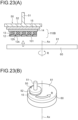
- FIGS. 23(A) and 23(B) are a cross-sectional view and a perspective view schematically showing the process of polishing the semiconductor layers 12.
- the glass substrate 15 of the intermediate structure 110B is fixed to the carrier 50 of the polishing device.
- the polishing device and the polishing method are as described in the first embodiment.
- the rotation of the polishing plate 60 is stopped at a constant time interval, and the polishing worker detaches the intermediate structure 110B from the carrier 50 and visually observes the polished surfaces of the semiconductor layers 12.
- the finish thickness of the semiconductor layers 12 can be controlled precisely.
- the slurry flows in the grooves 101 between the islands each including the semiconductor layer 12 and the support 13, and thus the slurry is fed to the first surfaces 12s of all the semiconductor layers 12 and the polishing effect is enhanced. Accordingly, the polished surface of the semiconductor layer 12 can be smoothed with ease so that the surface roughness becomes less than or equal to 10 nm.
- the semiconductor layers 12 is supported via the support 13 having a greater thickness and a lower Young's modulus than the semiconductor layer 12, the load acting on the semiconductor layer 12 at the time of the polishing is reduced and the occurrence of the cracking or chipping of the first surface 12s of the semiconductor layer 12 can be prevented.
- a semiconductor layer support structure 120B including a plurality of islands each including the semiconductor layer 12 and the support 13, the adhesive member 14 and the glass substrate 15 is obtained as shown in FIG. 24 .
- FIGS. 25(A), 25(B) and 25(C) are schematic diagrams showing a process of joining the semiconductor layers 12 to the silicon substrate 21, a process of removing the adhesive member 14 and a process of removing the support 13.
- the polished surfaces of the semiconductor layers 12 of the semiconductor layer support structure 120B detached from the carrier 50 are joined to the silicon substrate 21 as the transfer substrate as shown in FIG. 25(A) .
- the polished surfaces of the semiconductor layers 12 are joined to the surface of the silicon substrate 21 by intermolecular force.
- the adhesive member 14 is removed as shown in FIG. 25 (B) .
- the adhesive member 14 is the adhesive sheet of the thermal release type ( FIG. 21(A) )
- the adhesive member 14 can be peeled off by erasing the adhesive force of the adhesive member 14 by heating the adhesive member 14 up to a prescribed temperature.
- the adhesive member 14 is the adhesive layer 140 ( FIG. 21(B) )
- the adhesive member 14 can be removed by dissolving the adhesive layer 140 in a solvent, for example.
- the support 13 is removed as shown in FIG. 25(C) .
- the support 13 can be removed by dissolving the support 13 in an organic solvent, for example.
- a base substrate 130B in which a plurality of semiconductor layers 12 are arrayed in a grid on the silicon substrate 21 is obtained.
- the semiconductor layer 12 is referred to also as the semiconductor element.
- the semiconductor layer 12 of the base substrate 130B is patterned as described in the first embodiment and thereby made into an LED, for example.
- the adhesive member 14, the glass substrate 15 and the disk part 52 of the carrier 50 may also be provided with the through holes 14h, 15h and 52h at positions overlapping with the holes 12h of the semiconductor layers 12. With such a configuration, whether the hole 12h has penetrated the semiconductor layer 12 or not can be checked by using the optical device 65 ( FIG. 15(B) ) described in the second embodiment.
- the semiconductor layer 12 is supported via the support 13, and thus the stress or the like applied to the semiconductor layer 12 in the polishing process can be absorbed by the support 13 and the load acting on the semiconductor layer 12 can be reduced. Accordingly, the occurrence of the cracking or chipping of the polished surface of the semiconductor layer 12 can be inhibited.
- the fourth embodiment differs from the first embodiment in that a semiconductor layer 32 includes a cutout part 32c instead of the hole 12h.
- FIG. 27 is a flowchart showing a manufacturing method of a semiconductor element in the fourth embodiment.
- FIG. 28 is a plan view schematically showing the semiconductor layers 32 separated on the sapphire substrate 11.
- FIG. 29 is a perspective view schematically showing the shape of the semiconductor layer 32.
- FIG. 30 is a perspective view schematically showing a state in which a support 33 has been formed on the semiconductor layer 32.
- the processes of forming the semiconductor thin-film layer on the sapphire substrate 11 and patterning the semiconductor thin-film layer and thereby separating (singulating) the semiconductor thin-film layer into the semiconductor layers 32 are as described in the first embodiment.
- the semiconductor layer 32 is referred to also as the semiconductor thin film (or the semiconductor thin film piece).
- the semiconductor layers 32 are separated in a grid pattern by the grooves 101 extending in two directions orthogonal to each other.
- the shape of the semiconductor layer 32 is a quadrangular shape, more specifically, a square shape with each side 1 mm to 10 mm long.
- the shape of the semiconductor layer 32 is not limited to the square shape but may also be a rectangular shape or a different shape.
- the semiconductor layer 32 has a first surface 32s facing the sapphire substrate 11 and a second surface 32t on the opposite side.
- the semiconductor layer 32 has a shape obtained by cutting away four corner parts of a quadrangle. Namely, the semiconductor layer 32 has four cutout parts 32c.
- the cutout part 32c as the polishing indication part extends from the second surface 32t toward the first surface 32s, the cutout part 32c does not reach the first surface 32s.
- the extending direction of the cutout part 32c is a direction orthogonal to the first surface 32s and the second surface 32t, for example.
- a base part 32b is formed on the first surface 32s side of the cutout part 32c.
- the base part 32b projects outward from the cutout part 32c on a plane parallel to the first surface 32s.
- the cutout part 32c and the base part 32b are also referred to collectively as a step part 32a.
- the support 33 has a first surface 33s facing the semiconductor layer 32 and a second surface 33t on the opposite side.
- the two-dimensional shape of the support 33 is the same as the two-dimensional shape of the semiconductor layer 32 (excluding the base parts 32b).
- the support 33 has a shape obtained by cutting away four corner parts of a quadrangle. Namely, the support 33 has four cutout parts 33c.
- the cutout part 33c extends from the first surface 33s to the second surface 33t.
- the cutout parts 33c of the support 33 are situated at positions overlapping with the cutout parts 32c of the semiconductor layer 32.
- FIGS. 31(A) to 31(C) are diagrams schematically showing a process of forming the cutout parts 32c in the semiconductor layer 32, a process of forming a support layer 33a and a process of separating (singulating) the support layer 33a.
- FIGS. 31(A) to 31(C) correspond to cross-sectional views taken along the line 31A - 31A shown in FIG. 28 .
- the cutout parts 32c are formed in the semiconductor layers 32 on the sapphire substrate 11 by means of photolithography, for example.
- the depth of the cutout part 32c is less than the thickness of the semiconductor layer 32. Therefore, the base part 32b is formed under the cutout part 32c.
- the semiconductor layers 32 (P1 to P29) shown in FIG. 28 include the cutout parts 32c in this example, it is sufficient that at least one semiconductor layer 32 includes the cutout parts 32c. Further, the one semiconductor layer 32 does not need to include four cutout parts 32c, and it is sufficient that the one semiconductor layer 32 includes at least one cutout part 32c.
- the support layer 33a is formed to cover the semiconductor layers 32 as shown in FIG. 31(B) .
- the thickness and the material of the support layer 33a are the same as those of the support layer 13a in the third embodiment.
- the support layer 33a is patterned by means of photolithography and thereby separated (singulated) into a plurality of supports 33 similarly to the semiconductor layers 32.
- the cutout parts 33c are formed in the supports 33.
- a semiconductor substrate 100C in which a plurality of islands (stacked structures), each made by stacking the semiconductor layer 32 and the support 33, are formed on the sapphire substrate 11 is formed.
- the supports 33 on the semiconductor layers 32 are joined to the glass substrate 15 via the adhesive member 14 ( FIG. 32(A) which will be explained later) as described in the third embodiment.
- the adhesive member 14 is as described in the first embodiment.
- FIGS. 32 (A) to 32(C) are cross-sectional views schematically showing the process of peeling off the semiconductor layers 32 from the sapphire substrate 11.
- the laser light is applied to the semiconductor layer 32 from the sapphire substrate 11 side of the semiconductor substrate 100C. Accordingly, the semiconductor layers 32 peel off from the sapphire substrate 11 as shown in FIG. 32(B) .
- an intermediate structure (pre-polishing structure) 110C including a plurality of islands each including the semiconductor layer 32 and the support 33, the adhesive member 14 and the glass substrate 15 is obtained as shown in FIG. 32(C) .
- FIGS. 33(A) and 33(B) are a cross-sectional view and a perspective view schematically showing the process of polishing the semiconductor layers 32.
- the glass substrate 15 of the intermediate structure 110C is fixed to the carrier 50 of the polishing device.
- the polishing device and the polishing method are as described in the first embodiment.
- the semiconductor layer 32 is provided with the cutout parts 32c formed to extend from the second surface 32t toward the first surface 32s.
- the cutout part 32c has a depth not to reach the first surface 32s.
- the depth of the cutout part 32c has been set at a desired finish thickness of the semiconductor layer 32.
- the rotation of the polishing plate 60 is stopped at a constant time interval as described in the first embodiment. Then, the polishing worker detaches the intermediate structure 110C from the carrier 50 and visually observes the polished surfaces of the semiconductor layers 32.
- the cutout part 32c is not exposed to the polished surface until the polishing amount of the semiconductor layer 32 from the first surface 32s reaches a certain amount.
- the intermediate structure 110C is reattached to the carrier 50, the rotation of the polishing plate 60 is started, and the polishing is restarted.
- the time from the start (restart) of the polishing to the next stoppage of the polishing is determined so that the polishing amount in the time equals a prescribed amount in consideration of the revolution speed of the polishing plate 60, the polishing rate, and the target thickness of the semiconductor layer 32.
- the polishing amount reaches a prescribed amount
- the cutout part 32c is exposed to the polished surface.
- the base part 32b disappears and the cutout part 32c penetrates the semiconductor layer 32.
- the finish thickness of the semiconductor layer 32 can be controlled to be equal to the depth of the cutout part 32c.
- a semiconductor layer support structure 120C including a plurality of islands each including the semiconductor layer 32 and the support 33, the adhesive member 14 and the glass substrate 15 is obtained as shown in FIG. 34 .
- FIGS. 35(A), 35(B) and 35(C) are schematic diagrams showing a process of joining the semiconductor layers 32 to the silicon substrate 21, a process of removing the adhesive member 14 and a process of removing the support 33.
- step S107 the polished surfaces of the semiconductor layers 32 of the semiconductor layer support structure 120C detached from the carrier 50 are joined to the silicon substrate 21 as the transfer substrate as shown in FIG. 35(A) .
- the adhesive member 14 is removed as shown in FIG. 35(B) .
- the method of removing the adhesive member 14 is as described in the first embodiment.
- the support 33 is removed as shown in FIG. 35 (C) .
- the method of removing the support 33 is as described in the third embodiment.
- a base substrate 130C in which a plurality of semiconductor layers 32 are arrayed in a grid on the silicon substrate 21 is obtained.
- the semiconductor layer 32 is referred to also as the semiconductor element.
- the semiconductor layer 32 of the base substrate 130C is patterned as described in the first embodiment and thereby made into an LED, for example.
- the cutout part 32c in the fourth embodiment is formed to cut away a corner part of the semiconductor layer 32 in this example
- the cutout part 32c is not limited to such a configuration.
- the cutout part 32c may also be formed on a side face of the semiconductor layer 32 as a groove (for example, U-shaped groove or V-shaped groove) extending from the second surface 32t toward the first surface 32s.
- the adhesive member 14, the glass substrate 15 and the disk part 52 of the carrier 50 may also be provided with the through holes 14h, 15h and 52h (see FIG. 15(A) ) overlapping with the cutout parts 32c of the semiconductor layers 12. With such a configuration, whether the cutout part 32c has penetrated the semiconductor layer 32 or not can be checked by using the optical device 65 ( FIG. 15(B) ) described in the second embodiment.
- the semiconductor layer 32 includes the cutout part 32c as the polishing indication part extending from the second surface 32t toward the first surface 32s. Therefore, the finish thickness of the semiconductor layer 32 can be controlled at the target thickness by previously forming the cutout part 32c having a depth equal to the target thickness of the semiconductor layer 32 and executing the polishing until the cutout part 32c is exposed to the polished surface (i.e., until the base part 32b disappears).
- the present disclosure is applicable to a manufacturing method of a semiconductor element such as an LED and to a semiconductor layer support structure and a semiconductor substrate used for the manufacture of semiconductor elements.
Landscapes
- Engineering & Computer Science (AREA)
- Microelectronics & Electronic Packaging (AREA)
- Manufacturing & Machinery (AREA)
- Computer Hardware Design (AREA)
- Power Engineering (AREA)
- Physics & Mathematics (AREA)
- Condensed Matter Physics & Semiconductors (AREA)
- General Physics & Mathematics (AREA)
- Mechanical Treatment Of Semiconductor (AREA)
Applications Claiming Priority (1)
| Application Number | Priority Date | Filing Date | Title |
|---|---|---|---|
| JP2022173002A JP2024064422A (ja) | 2022-10-28 | 2022-10-28 | 半導体素子の製造方法、半導体層支持構造体、および半導体基板 |
Publications (1)
| Publication Number | Publication Date |
|---|---|
| EP4362066A1 true EP4362066A1 (en) | 2024-05-01 |
Family
ID=87557891
Family Applications (1)
| Application Number | Title | Priority Date | Filing Date |
|---|---|---|---|
| EP23189698.6A Pending EP4362066A1 (en) | 2022-10-28 | 2023-08-04 | Manufacturing method of semiconductor element, semiconductor layer support structure, and semiconductor substrate |
Country Status (5)
| Country | Link |
|---|---|
| US (1) | US20240145631A1 (ja) |
| EP (1) | EP4362066A1 (ja) |
| JP (1) | JP2024064422A (ja) |
| CN (1) | CN117954535A (ja) |
| TW (1) | TW202418381A (ja) |
Citations (6)
| Publication number | Priority date | Publication date | Assignee | Title |
|---|---|---|---|---|
| JP2006086388A (ja) | 2004-09-17 | 2006-03-30 | Sony Corp | 半導体薄膜の表面処理方法、及び半導体素子の分離方法 |
| US20090079025A1 (en) * | 2007-09-21 | 2009-03-26 | Semiconductor Energy Laboratory Co., Ltd. | Substrate provided with semiconductor films and manufacturing method thereof |
| US20110037051A1 (en) * | 2007-08-10 | 2011-02-17 | Hong Kong Applied Science and Technology Research Institute Company Limited | Optimization of polishing stop design |
| CN103890914A (zh) * | 2011-09-28 | 2014-06-25 | Bbsa有限公司 | 半导体元件及其制造方法 |
| US20140319557A1 (en) * | 2011-05-12 | 2014-10-30 | Dowa Electronics Materials Co., Ltd. | Vertically structured group iii nitride semiconductor led chip and method for manufacturing the same |
| US20180226471A1 (en) * | 2017-02-03 | 2018-08-09 | Infineon Technologies Ag | Method of Manufacturing Semiconductor Devices by Using Epitaxy and Semiconductor Devices with a Lateral Structure |
-
2022
- 2022-10-28 JP JP2022173002A patent/JP2024064422A/ja active Pending
-
2023
- 2023-08-04 EP EP23189698.6A patent/EP4362066A1/en active Pending
- 2023-08-08 US US18/446,271 patent/US20240145631A1/en active Pending
- 2023-08-14 TW TW112130440A patent/TW202418381A/zh unknown
- 2023-08-17 CN CN202311036694.XA patent/CN117954535A/zh active Pending
Patent Citations (6)
| Publication number | Priority date | Publication date | Assignee | Title |
|---|---|---|---|---|
| JP2006086388A (ja) | 2004-09-17 | 2006-03-30 | Sony Corp | 半導体薄膜の表面処理方法、及び半導体素子の分離方法 |
| US20110037051A1 (en) * | 2007-08-10 | 2011-02-17 | Hong Kong Applied Science and Technology Research Institute Company Limited | Optimization of polishing stop design |
| US20090079025A1 (en) * | 2007-09-21 | 2009-03-26 | Semiconductor Energy Laboratory Co., Ltd. | Substrate provided with semiconductor films and manufacturing method thereof |
| US20140319557A1 (en) * | 2011-05-12 | 2014-10-30 | Dowa Electronics Materials Co., Ltd. | Vertically structured group iii nitride semiconductor led chip and method for manufacturing the same |
| CN103890914A (zh) * | 2011-09-28 | 2014-06-25 | Bbsa有限公司 | 半导体元件及其制造方法 |
| US20180226471A1 (en) * | 2017-02-03 | 2018-08-09 | Infineon Technologies Ag | Method of Manufacturing Semiconductor Devices by Using Epitaxy and Semiconductor Devices with a Lateral Structure |
Also Published As
| Publication number | Publication date |
|---|---|
| US20240145631A1 (en) | 2024-05-02 |
| TW202418381A (zh) | 2024-05-01 |
| CN117954535A (zh) | 2024-04-30 |
| JP2024064422A (ja) | 2024-05-14 |
Similar Documents
| Publication | Publication Date | Title |
|---|---|---|
| US8084335B2 (en) | Method of thinning a semiconductor wafer using a film frame | |
| US6713366B2 (en) | Method of thinning a wafer utilizing a laminated reinforcing layer over the device side | |
| US6699774B2 (en) | Wafer splitting method using cleavage | |
| US7294531B2 (en) | Wafer level chip stack method | |
| JP4791843B2 (ja) | 接着フィルム付きデバイスの製造方法 | |
| US7384858B2 (en) | Wafer dividing method | |
| KR100759687B1 (ko) | 기판의 박판화 방법 및 회로소자의 제조방법 | |
| TWI683358B (zh) | 半導體裝置之製造方法 | |
| JP2010206044A (ja) | 半導体装置の製造方法 | |
| CN100410343C (zh) | 用于制造供半导体生产使用的胶带的装置和方法 | |
| US20180158712A1 (en) | Method for Bonding Thin Semiconductor Chips to a Substrate | |
| US20090061596A1 (en) | Expanding tool, expanding method, and manufacturing method of unit elements | |
| JP2002118081A (ja) | 半導体装置の製造方法 | |
| US20050029628A1 (en) | Semiconductor device whose semiconductor chip has chamfered backside surface edges and method of manufacturing the same | |
| JPH11307488A (ja) | 半導体装置、その製造方法、加工ガイドおよびその加工装置 | |
| EP4362066A1 (en) | Manufacturing method of semiconductor element, semiconductor layer support structure, and semiconductor substrate | |
| JP2012156288A (ja) | 半導体チップの製造方法および半導体チップの実装方法 | |
| US20130264686A1 (en) | Semiconductor wafer processing | |
| EP4362065A1 (en) | Manufacturing method of semiconductor element, semiconductor layer support structure, and semiconductor substrate | |
| JP2007258245A (ja) | ウエハ付シートの製造方法、円盤状ウエハの外周部分分離方法、分離用シート、および分離用シートの製造方法 | |
| KR20030047705A (ko) | 반도체 웨이퍼 가공방법 및 이것에 사용되는 지지기판 | |
| JP2003124147A (ja) | 半導体装置の製造方法 | |
| JP2018206936A (ja) | 基板処理システム、基板処理方法 | |
| JP5090241B2 (ja) | ダイソート用シート | |
| US20070221318A1 (en) | Adhesion tape and method for mounting a chip onto a substrate |
Legal Events
| Date | Code | Title | Description |
|---|---|---|---|
| PUAI | Public reference made under article 153(3) epc to a published international application that has entered the european phase |
Free format text: ORIGINAL CODE: 0009012 |
|
| STAA | Information on the status of an ep patent application or granted ep patent |
Free format text: STATUS: THE APPLICATION HAS BEEN PUBLISHED |
|
| AK | Designated contracting states |
Kind code of ref document: A1 Designated state(s): AL AT BE BG CH CY CZ DE DK EE ES FI FR GB GR HR HU IE IS IT LI LT LU LV MC ME MK MT NL NO PL PT RO RS SE SI SK SM TR |