EP4344385B1 - Halbleiterstruktur und herstellungsverfahren dafür - Google Patents
Halbleiterstruktur und herstellungsverfahren dafür Download PDFInfo
- Publication number
- EP4344385B1 EP4344385B1 EP22922574.3A EP22922574A EP4344385B1 EP 4344385 B1 EP4344385 B1 EP 4344385B1 EP 22922574 A EP22922574 A EP 22922574A EP 4344385 B1 EP4344385 B1 EP 4344385B1
- Authority
- EP
- European Patent Office
- Prior art keywords
- pillar
- semiconductor
- gate
- dielectric layer
- layer
- Prior art date
- Legal status (The legal status is an assumption and is not a legal conclusion. Google has not performed a legal analysis and makes no representation as to the accuracy of the status listed.)
- Active
Links
Images


Classifications
-
- H—ELECTRICITY
- H10—SEMICONDUCTOR DEVICES; ELECTRIC SOLID-STATE DEVICES NOT OTHERWISE PROVIDED FOR
- H10D—INORGANIC ELECTRIC SEMICONDUCTOR DEVICES
- H10D30/00—Field-effect transistors [FET]
- H10D30/60—Insulated-gate field-effect transistors [IGFET]
- H10D30/67—Thin-film transistors [TFT]
- H10D30/6728—Vertical TFTs
-
- H—ELECTRICITY
- H10—SEMICONDUCTOR DEVICES; ELECTRIC SOLID-STATE DEVICES NOT OTHERWISE PROVIDED FOR
- H10B—ELECTRONIC MEMORY DEVICES
- H10B12/00—Dynamic random access memory [DRAM] devices
- H10B12/01—Manufacture or treatment
-
- H—ELECTRICITY
- H10—SEMICONDUCTOR DEVICES; ELECTRIC SOLID-STATE DEVICES NOT OTHERWISE PROVIDED FOR
- H10B—ELECTRONIC MEMORY DEVICES
- H10B12/00—Dynamic random access memory [DRAM] devices
- H10B12/30—DRAM devices comprising one-transistor - one-capacitor [1T-1C] memory cells
- H10B12/48—Data lines or contacts therefor
- H10B12/488—Word lines
-
- G—PHYSICS
- G11—INFORMATION STORAGE
- G11C—STATIC STORES
- G11C8/00—Arrangements for selecting an address in a digital store
- G11C8/14—Word line organisation; Word line lay-out
-
- H—ELECTRICITY
- H10—SEMICONDUCTOR DEVICES; ELECTRIC SOLID-STATE DEVICES NOT OTHERWISE PROVIDED FOR
- H10B—ELECTRONIC MEMORY DEVICES
- H10B12/00—Dynamic random access memory [DRAM] devices
- H10B12/01—Manufacture or treatment
- H10B12/02—Manufacture or treatment for one transistor one-capacitor [1T-1C] memory cells
-
- H—ELECTRICITY
- H10—SEMICONDUCTOR DEVICES; ELECTRIC SOLID-STATE DEVICES NOT OTHERWISE PROVIDED FOR
- H10B—ELECTRONIC MEMORY DEVICES
- H10B12/00—Dynamic random access memory [DRAM] devices
- H10B12/20—DRAM devices comprising floating-body transistors, e.g. floating-body cells
-
- H—ELECTRICITY
- H10—SEMICONDUCTOR DEVICES; ELECTRIC SOLID-STATE DEVICES NOT OTHERWISE PROVIDED FOR
- H10B—ELECTRONIC MEMORY DEVICES
- H10B12/00—Dynamic random access memory [DRAM] devices
- H10B12/30—DRAM devices comprising one-transistor - one-capacitor [1T-1C] memory cells
- H10B12/48—Data lines or contacts therefor
- H10B12/482—Bit lines
-
- H—ELECTRICITY
- H10—SEMICONDUCTOR DEVICES; ELECTRIC SOLID-STATE DEVICES NOT OTHERWISE PROVIDED FOR
- H10D—INORGANIC ELECTRIC SEMICONDUCTOR DEVICES
- H10D30/00—Field-effect transistors [FET]
- H10D30/01—Manufacture or treatment
- H10D30/021—Manufacture or treatment of FETs having insulated gates [IGFET]
- H10D30/025—Manufacture or treatment of FETs having insulated gates [IGFET] of vertical IGFETs
-
- H—ELECTRICITY
- H10—SEMICONDUCTOR DEVICES; ELECTRIC SOLID-STATE DEVICES NOT OTHERWISE PROVIDED FOR
- H10D—INORGANIC ELECTRIC SEMICONDUCTOR DEVICES
- H10D30/00—Field-effect transistors [FET]
- H10D30/60—Insulated-gate field-effect transistors [IGFET]
- H10D30/63—Vertical IGFETs
-
- H—ELECTRICITY
- H10—SEMICONDUCTOR DEVICES; ELECTRIC SOLID-STATE DEVICES NOT OTHERWISE PROVIDED FOR
- H10D—INORGANIC ELECTRIC SEMICONDUCTOR DEVICES
- H10D30/00—Field-effect transistors [FET]
- H10D30/60—Insulated-gate field-effect transistors [IGFET]
- H10D30/67—Thin-film transistors [TFT]
- H10D30/674—Thin-film transistors [TFT] characterised by the active materials
- H10D30/6755—Oxide semiconductors, e.g. zinc oxide, copper aluminium oxide or cadmium stannate
-
- H—ELECTRICITY
- H10—SEMICONDUCTOR DEVICES; ELECTRIC SOLID-STATE DEVICES NOT OTHERWISE PROVIDED FOR
- H10D—INORGANIC ELECTRIC SEMICONDUCTOR DEVICES
- H10D84/00—Integrated devices formed in or on semiconductor substrates that comprise only semiconducting layers, e.g. on Si wafers or on GaAs-on-Si wafers
- H10D84/80—Integrated devices formed in or on semiconductor substrates that comprise only semiconducting layers, e.g. on Si wafers or on GaAs-on-Si wafers characterised by the integration of at least one component covered by groups H10D12/00 or H10D30/00, e.g. integration of IGFETs
- H10D84/82—Integrated devices formed in or on semiconductor substrates that comprise only semiconducting layers, e.g. on Si wafers or on GaAs-on-Si wafers characterised by the integration of at least one component covered by groups H10D12/00 or H10D30/00, e.g. integration of IGFETs of only field-effect components
- H10D84/83—Integrated devices formed in or on semiconductor substrates that comprise only semiconducting layers, e.g. on Si wafers or on GaAs-on-Si wafers characterised by the integration of at least one component covered by groups H10D12/00 or H10D30/00, e.g. integration of IGFETs of only field-effect components of only insulated-gate FETs [IGFET]
Definitions
- the disclosure relates to the technical field of semiconductor manufacturing, in particular to a semiconductor structure and a method for manufacturing the same.
- DRAM Dynamic random access memory
- Embodiments of the disclosure provide a semiconductor structure and a method for manufacturing a semiconductor structure.
- Embodiments of the disclosure provide a semiconductor structure and a method for manufacturing the same.
- the semiconductor structure includes: a substrate; a semiconductor pillar located on the substrate and a gate pillar located on the semiconductor pillars, in which the semiconductor pillar and the gate pillar both extend in a direction perpendicular to a plane of the substrate; a first word line extending in a first direction parallel to the plane of the substrate and surrounding the semiconductor pillar; and a semiconductor layer located above the semiconductor pillar and at least surrounding a sidewall of the gate pillar.
- the semiconductor pillar at the bottom and the semiconductor layer located thereon are longitudinally distributed.
- an area occupied by the projections of two transistors on the substrate can be significantly reduced compared with the case that two transistors are tiled on the substrate, thereby effectively improving the integration level of the semiconductor structure by the embodiments of the disclosure.
- first, second, third and the like may be used to describe various elements, components, regions, layers and/or sections, these elements, components, regions, layers and/or sections should not be limited by these terms. These terms are only used to distinguish one element, component, region, layer or section from another element, component, region, layer or section. Therefore, without departing from the teaching of the disclosure, a first element, component, region, layer or section discussed below may be represented as a second element, component, region, layer or section. While the second element, component, region, layer or section is discussed, it does not mean that the first element, component, region, layer or section is necessarily present in the disclosure.
- Spatial relation terms such as “under ", “below ", “lower”, “underneath", “above ", “upper” and the like, may be used herein for conveniently describing a relationship between one element or feature and another element or feature shown in the drawings. It should be understood that in addition to orientations shown in the drawings, the spatial relation terms are intended to further include the different orientations of a device in use and operation. For example, if the device in the drawings is turned over, then the elements or the features described as “below” or “underneath” or “under” other elements may be oriented “on” the other elements or features. Therefore, the exemplary terms “below " and “under " may include two orientations of up and down. The device may be otherwise oriented (rotated by 90 degrees or other orientations) and the spatial relation terms used here are interpreted accordingly.
- a memory cell In a common dynamic random access memory (DRAM), a memory cell usually consists of one transistor and one capacitor (1T1C), and the capacitor is used to store data.
- 1T1C DRAM has high requirements for an amount of charge stored in the capacitor. Reading operation to the capacitor is destructive, which requires the data to be rewritten after the reading operation, thereby increasing the power consumption. Meanwhile, because of the complex manufacturing process and high occupied volume, the miniaturization of the capacitors becomes a problem.
- the embodiments of the disclosure provide a semiconductor structure.
- the semiconductor structure includes: a substrate; a semiconductor pillar located on the substrate and a gate pillar located on the semiconductor pillar, in which the semiconductor pillar and the gate pillar both extend in a direction perpendicular to a plane of the substrate; a first word line extending in a first direction parallel to the plane of the substrate and surrounding the semiconductor pillar; and a semiconductor layer located above the semiconductor pillar and at least surrounding a sidewall of the gate pillar.
- the semiconductor pillar at the bottom and the semiconductor layer located thereon are longitudinally distributed. Therefore, when a transistor structure is subsequently formed on the semiconductor pillar and the semiconductor layer, an area occupied by the projections of two transistors on the substrate can be significantly reduced, compared with the case that two transistors are distributed laterally on the substrate, thereby effectively improving the integration level of the semiconductor structure by the embodiments of the disclosure.
- FIG. 1 schematically shows a structure of a semiconductor structure provided by an embodiment of the disclosure.
- FIG. 2 schematically shows another structure of a semiconductor structure provided by an embodiment of the disclosure.
- FIG. 3 schematically shows yet another structure of semiconductor structure provided by an embodiment of the disclosure.
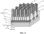
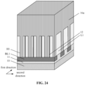
- the semiconductor structure includes: a substrate 10; a semiconductor pillar 13 located on the substrate 10 and a gate pillar 18 located on the semiconductor pillar 13, in which the semiconductor pillar 13 and the gate pillar 18 both extend in a direction perpendicular to the plane of substrate 10; a first word line WL1 extending in a first direction parallel to the plane of the substrate 10 and surrounding the semiconductor pillar 13; and a semiconductor layer 16 located on the semiconductor pillar 13 and at least surrounding a sidewall of the gate pillar 18.
- the gate pillar 18 and the semiconductor pillar 13 are in one-to-one correspondence.
- the substrate may be a semiconductor substrate and may specifically include at least one elemental semiconductor material (such as silicon (Si) substrate, germanium (Ge) substrate), at least one III-V compound semiconductor material (such as gallium nitride (GaN) substrate, gallium arsenide (GaAs) substrate, indium phosphide (InP) substrate), at least one II-VI compound semiconductor material, at least one organic semiconductor material, or other semiconductor materials known in the art.
- the substrate is the silicon substrate.
- materials of the semiconductor pillar 13 and the semiconductor layer 16 include at least one or a combination of indium oxide, tin oxide, In-Zn oxide, Sn-Zn oxide, Al-Zn oxide, In-Ga oxide, In-Ga-Zn oxide, In-Al-Zn oxide, In-Sn-Zn oxide, Sn-Ga-Zn oxide, Al-Ga-Zn oxide, or Sn-Al-Zn oxide.
- the materials of the semiconductor pillar and the semiconductor layer may also include In-Hf-Zn oxide, In-La-Zn oxide, In-Ce-Zn oxide, In-Pr-Zn oxide, In-Nd-Zn oxide, In-Sm-Zn oxide, In-Eu-Zn oxide, In-Gd-Zn oxide, In-Tb-Zn oxide, In-Dy-Zn oxide, In-Ho-Zn oxide, In-Er-Zn oxide, In-Tm-Zn oxide, In-Yb-Zn oxide, In-Lu-Zn oxide; or quaternary metal oxide such as In-Sn-Ga-Zn oxide, In-Hf-Ga-Zn oxide, In-Al-Ga-Zn oxide, In-Sn-Al-Zn oxide, In-Sn-Hf-Zn oxide, In-Hf-Al-Zn oxide, etc.
- a material containing at least indium (In) or zinc (Zn) may be selected as the material for the semiconductor pillar and the semiconductor layer.
- the material containing indium (In) and zinc (Zn) are preferred.
- a material further containing a stabilizer, gallium (Ga) element may be selected. The stabilizer can reduce electrical characteristic deviation of the finally formed transistor.
- the materials of the semiconductor pillar and the semiconductor layer include, but are not limited to, indium gallium zinc oxide (IGZO), such as the material with chemical formula of InGaZnO 4 .
- IGZO indium gallium zinc oxide
- the materials of the semiconductor pillar and the semiconductor layer include In x Ga y Zn 1-x-y O, where x is greater than or equal to 0 or less than or equal to 1 and y is greater than or equal to 0 or less than or equal to 1.
- part of the semiconductor pillar may be used as a channel region, and the semiconductor layer may be used as a channel region.
- a transistor structure for writing operation and a transistor structure for reading operation may be formed, respectively.
- an oxide semiconductor material when used for forming the semiconductor pillar and the semiconductor layer, that is, when the oxide semiconductor material is used for forming the channel region of the transistor structure for writing operation and the channel region of the transistor structure for reading operation, it can effectively reduce the leakage current of the two transistor structures, improve the on-off current ratio and current drivability of the two transistor structures, increase an access speed of the semiconductor structure, and reduce power consumption, as the oxide semiconductor material has higher carrier mobility and lower leakage current.
- the transistor structure formed based on semiconductor pillar can be used as a write transistor of the semiconductor structure, and the transistor structure formed based on the semiconductor layer can be used as a read transistor of the semiconductor structure.
- One write transistor and one read transistor constitute one memory cell, which is configured to realize the reading operation of information.
- the structure provided by the embodiment of the disclosure neither needs additional capacitor manufacturing, thus simplifying the process, nor needs re-writing operation after reading operation, thus reducing power consumption.
- the semiconductor pillar 13 includes a first electrode 131, a first channel region 132, and a second electrode 133 distributed from bottom to top.
- the first electrode 131, the first channel region 132, and the second electrode 133 are the same in term of conductivity type.
- the material of the semiconductor pillar is indium gallium zinc oxide (IGZO)
- IGZO indium gallium zinc oxide
- the first electrode 131, the first channel region 132 and the second electrode 133 may be used as a first source/drain region, a channel region, and a second source/drain region of the write transistor respectively.
- the semiconductor layer 16 includes a first sub-portion 161, a second sub-portion 162, and a third sub-portion 163 connected to each other.
- the first sub-portion 161 covers a top surface of the gate pillar 18, the second sub-portion 162 covers a sidewall of the gate pillar 18, and the third sub-portion 163 partially covers an upper surface of the substrate 10 between adjacent gate pillars 18.
- the channel region of the read transistor since the semiconductor layer can be used as a channel region of the read transistor, and the second sub-portion of thereof covers (surrounds) the sidewall of the gate pillar, the channel region of the read transistor has a larger channel size compared with a structure that a channel region is only arranged on one side of a gate, thereby effectively preventing the occurrence of the short channel effect by the structure provided by the embodiment of the disclosure.
- the semiconductor structure further includes a first gate dielectric layer 14, and a second gate dielectric layer 15.
- the first gate dielectric layer 14 is located between the first word line WL1 and the semiconductor pillar 13, and surrounds the first channel region 132 and the second electrode 133.
- the second gate dielectric layer 15 includes a first sub-layer 151 and a second sub-layer 152 connected to each other.
- the first sub-layer 151 is located between the gate pillar 18 and the semiconductor layer 16, covers the top and the sidewall of the gate pillar 18.
- the second sub-layer 152 covers an upper surface of the substrate 10 between the adjacent gate pillars 18.
- the semiconductor structure further includes a first gate dielectric layer 14, a second gate dielectric layer 15 and a fourth dielectric layer L4.
- the first gate dielectric layer 14 is located between the first word line WL1 and the semiconductor pillar 13, and surrounds the first channel region 132 and the second electrode 133.
- the second gate dielectric layer 15 covers the top and the sidewall of the gate pillar 18.
- the fourth dielectric layer L4 covers the upper surface of the substrate 10 between adjacent gate pillars 18.
- materials of the first gate dielectric layer and the second gate dielectric layer include, but are not limited to, oxides, nitrides, oxynitride, and other insulating materials, etc.
- the materials of the first gate dielectric layer and the second gate dielectric layer may be one or a combination of alumina, silicon oxide, silicon nitride, etc.
- the process for forming the first gate dielectric layer and the second gate dielectric layer includes, but is not limited to, an atomic layer deposition process and the like.
- the second gate dielectric layer includes the portion covering the upper surface of the substrate between the adjacent gate pillars, the structure located at lower and around the semiconductor pillar is electrically isolated from the structure located at upper and around the gate pillar, thereby preventing mutual interference between the above structures.
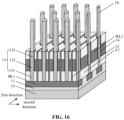
- the semiconductor structure further includes a second word line WL2, a first bit line BL1 and a second bit line BL2.
- the second word lines WL2 extends in the first direction, surrounds an end, close to the semiconductor pillar 13 of the second sub-portion 162, and covers the upper surface of the third sub-portion 163.
- the first bit line BL1 and the second bit line BL2 extend in a second direction parallel to the plane of the substrate 10 and perpendicular to the first direction.
- the first bit line BL1 is located below the semiconductor pillar 13 and electrically connected to the lower portion of the semiconductor pillar 13.
- the second bit line BL2 is located above the semiconductor layer 16 and electrically connected to the first sub-portion 161.
- the second word line can be used as the source region or drain region of the read transistor, while the second bit line can be used as the drain region or source region of the read transistor.
- the second word line is used as the source region of the read transistor, and the second bit line is used as the drain region of the read transistor, but is not limited to this.
- the second word line may be used as the drain region of the read transistor, and the second bit line may be used as the source region of the read transistor, which is not specifically limited herein.
- the contact area between the second word line and the channel region is increased, which is beneficial to reduce a contact resistance between the second word line and the channel region, thereby reducing the power consumption of the read transistor.
- the first bit line may be electrically connected to the first electrode of the semiconductor pillar.
- the charge can be injected into gate (i.e., the gate pillar) of the read transistor through the semiconductor pillar, and the change in the amount of charges contained in the gate (i.e., the gate pillar) would affect the resistance state of the read transistor, thereby realizing the distinction between "0" and "1" in actual operation.
- the gate of the read transistor is used as a node for information storage, so that a separate process of forming a capacitor structure is unnecessary.
- the charge in the write transistor needs to be injected into the gate pillar of the read transistor through the semiconductor pillar. Therefore, the relative position and the connection relationship between the semiconductor pillar and the gate pillar, as well as material characteristics thereof may affect the transmission speed and efficiency of the charge
- the top of the semiconductor pillar 13 is electrically connected to the bottom of the gate pillar 18.
- the material of the semiconductor pillar may be an oxide semiconductor material
- the material of the gate pillar may include, but is not limited to, one or more of tungsten (W), copper (Cu), titanium (Ti), tantalum (Ta), titanium nitride (TiN), tantalum nitride (TaN), metal silicide, and metal alloy.
- the top of the second electrode of the semiconductor pillar is electrically connected to the bottom of the gate pillar directly. That is, the source/drain region of the write transistor is electrically connected to the gate of the read transistor directly without using other conductive wires.
- the embodiment of the disclosure can effectively shorten the charge flow path when the charge in the write transistor is injected into the gate of the read transistor, thereby effectively improving the transmission speed and efficiency of information of the semiconductor structure.
- the orthographic projection of the semiconductor pillar is at least partially overlapped with the orthographic projection of the gate pillar on the plane of the substrate.
- the material of the gate pillar is the same as that of the semiconductor pillar.
- the orthographic projection of the semiconductor pillar is at least partially overlapped with the orthographic projection of the gate pillar on the plane of the substrate. That is, the orthographic projection of the write transistor is at least partially overlapped with the orthographic projection of the read transistor on the plane of the substrate, so that the memory cell structure composed of one write transistor and one read transistor occupies less surface area of the substrate, which means that on the substrate with the same plane area, the semiconductor structure provided by the embodiment of the disclosure can be arranged with more memory cells. That is, the semiconductor structure of the embodiment of the disclosure can have higher integration.
- the semiconductor structure provided by the embodiment of the disclosure can be arranged with a better amount of memory cells, that is, the semiconductor structure of the embodiment of the disclosure can have a better integration.
- the material of the gate pillar is the same as that of the semiconductor pillar in the embodiment of the disclosure, that is, the material of the source/drain region of the write transistor is the same as that of the gate of the read transistor, so that when the source/drain region of the write transistor is electrically connected to the gate of the read transistor, there is no need to worry about an increase of contact resistance caused by the effect of metal-induced gap states between the metal material and the semiconductor material, thereby effectively reducing the power consumption of the whole semiconductor structure.
- materials of the semiconductor pillar and the gate pillar may include at least one or a combination of indium oxide, tin oxide, In-Zn oxide, Sn-Zn oxide, Al-Zn oxide, In-Ga oxide, In-Ga-Zn oxide, In-Al-Zn oxide, In-Sn-Zn oxide, Sn-Ga-Zn oxide, Al-Ga-Zn oxide, or Sn-Al-Zn oxide.
- the materials of the semiconductor pillar and the gate pillar may be an oxide semiconductor material, such as InGaZnO 4 material.
- the materials of the semiconductor pillar and the gate pillar include In x Ga y Zn 1-x-y O, where x is greater than or equal to 0, or less than or equal to 1 and y is greater than or equal to 0, or less than or equal to 1.
- the gate pillar 18 and the semiconductor pillar 13 are electrically connected directly.
- the gate pillar and the semiconductor pillar which are electrically connected directly form an integrated structure. That is, the channel region amd the source/drain region of the write transistor as well as the gate of the read transistor form the integrated structure. That is, the source/drain region of the write transistor and the gate of the read transistor can be electrically connected directly without using other conductive wires.
- the embodiment of the disclosure can effectively shorten the charge flow path when the charge in the write transistors is injected into the gate of the read transistor, thereby effectively improving the transmission speed and efficiency of information of the semiconductor structure.
- the charge in the write transistor needs to be injected into the gate of the read transistor through the source/drain region, it can effectively prevent the semiconductor structure from generating more heat during use, as there is no contact resistance in the integrated structure between the write transistor and the read transistor, thereby effectively improving the performance of the semiconductor structure.
- the structure composed of the gate pillar and the semiconductor pillar can be formed in the same process operation, which significantly reduces the complexity of the process and is beneficial to the improvement of production efficiency.
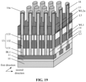
- the semiconductor structure further includes a first dielectric layer L1 located on the substrate 10 and a second dielectric layer L2 located on the first dielectric layer L1.
- the semiconductor pillar 13 and the first word line WL1 are located in the first dielectric layer L1, while the gate pillar 18, the semiconductor layer 16 and the second word line WL2 are located in the second dielectric layer L2.
- the semiconductor structure further includes a word line isolation structure 12 extending in the first direction.
- the word line isolation structure 12 is located between two adjacent first word lines WL1 to isolate the adjacent first word lines WL1.
- the word line isolation structure is located in the first dielectric layer.
- the material of the word line isolation structure may include, but is not limited to, oxide, nitride, oxynitride and the like, specifically, at least one or a combination of, for example, silicon oxide, silicon nitride, silicon oxynitride and the like.
- the embodiments of the disclosure also provide a method for manufacturing a semiconductor structure. As shown in FIG. 4 , the method includes the following operations.
- a pillar is formed on the substrate.
- the pillar includes a semiconductor pillar, and extends in a direction perpendicular to the plane of the substrate.
- a first word line is formed.
- the first word line extends in a first direction and surrounds part of the pillar.
- the first direction is parallel to a plane of the substrate.
- FIGS. 5 to 22 are process flow diagrams during a method for manufacturing a semiconductor structure provided by an embodiment of the disclosure.
- FIG. 23 schematically shows another structure of a semiconductor structure provided by an embodiment of the disclosure.
- S101 is performed. As shown in FIG. 5 , a substrate is provided.
- the substrate may be a semiconductor substrate, and specifically includes at least one elemental semiconductor material (such as silicon (Si) substrate, germanium (Ge) substrate), at least one III-V compound semiconductor material (such as gallium nitride (GaN) substrate, gallium arsenide (GaAs) substrate, indium phosphide (InP) substrate, etc.), at least one II-VI compound semiconductor material, at least one organic semiconductor material, or other semiconductor materials known in the art.
- the substrate is the silicon substrate.
- a pillar is formed on the substrate.
- the pillar includes a semiconductor pillar, and extends in a direction perpendicular to the plane of the substrate.
- the method further includes the following operations.
- An insulating layer 11 is formed on the substrate 10.
- An etching process is performed on the insulating layer 11, so as to form a plurality of first trenches T1 extending in a second direction in the insulating layer 11.
- the second direction is parallel to the plane of the substrate 10 and perpendicular to the first direction.
- the plurality of first trenches T1 are filled with a conductive material, to form a plurality of first bit lines BL1 extending in the second direction.
- the material of the insulating layer includes, but is not limited to, oxide, nitride, oxynitride and the like. In some specific embodiments, the material of the insulating layer may include, but is not limited to, silicon oxide and the like.
- the insulating layer and the conductive material may be formed by one or more thin film deposition process.
- the thin film deposition process includes, but is not limited to, a chemical vapor deposition (CVD) process, a plasma enhanced chemical vapor deposition (PECVD) process, an atomic layer deposition (ALD) process, or a combination thereof.
- CVD chemical vapor deposition
- PECVD plasma enhanced chemical vapor deposition
- ALD atomic layer deposition
- the method further includes the following operations.
- a first dielectric layer L1 is formed.
- the first dielectric layer L1 is etched to form a plurality of second trenches T2 extending in the first direction in the first dielectric layer L1.
- the plurality of second trenches T2 are filled with an insulating material to form a plurality of word line isolation structures 12 extending in the first direction.
- the material of the first dielectric layer includes, but is not limited to, one or an combination of oxide, nitride, oxynitride, another insulating material and the like. Specifically, the material of the first dielectric layer may include, but is not limited to, silicon oxide, silicon nitride and the like.
- the process for forming the first dielectric layer may be the same as or different from the process for forming the insulating layer, which is not specifically limited herein.
- the method before forming the pillar on the substrate, the method further includes the following operations.
- the first dielectric layer L1 is etched to form a plurality of first channel holes H1. Each of the first channel hole H1 exposes the first bit line BL1.
- Each of The first channel holes H1 is filled with a semiconductor material to form the pillar P.
- the pillar includes the semiconductor pillar 13.
- the plurality of first channel holes H1 may be formed by etching the first dielectric layer L1 from top to bottom.
- the plurality of first channel hole H1 are located in the first dielectric layer L1 between two adjacent word line isolation structures 12.
- the semiconductor pillar 13 may include a first electrode 131, a first channel region 132, and a second electrode 133 distributed from bottom to top.
- the first electrode 131, the first channel region 132, and the second electrode 133 have the same conductivity type. It is to be understood that, the first electrode 131, the first channel region 132 and the second electrode 133 may be used as the first source/drain region, the channel region and the second source/drain region of the transistor respectively.
- the material of the semiconductor pillar includes at least one or a combination of indium oxide, tin oxide, In-Zn oxide, Sn-Zn oxide, Al-Zn oxide, In-Ga oxide, In-Ga-Zn oxide, In-Al-Zn oxide, In-Sn-Zn oxide, Sn-Ga-Zn oxide, Al-Ga-Zn oxide, and Sn-Al-Zn oxide.
- the material of the semiconductor pillar includes, but is not limited to, indium gallium zinc oxide (IGZO), such as the material with a chemical formula of InGaZnO 4 .
- IGZO indium gallium zinc oxide
- the material of the semiconductor pillars includes In x Ga y Zn 1-x-y O, where x is greater than or equal to 0 or less than or equal to 1, and y is greater than or equal to 0 or less than or equal to 1.
- the transistor structure based on the semiconductor pillar may be subsequently formed by forming a control gate line, such as a word line structure, on part of the sidewall of the semiconductor pillar to control turn-on or turn-off of the channel region.
- a control gate line such as a word line structure
- the transistor structure formed based on the semiconductor pillar can be used as the write transistor of the memory.
- a first word line WL1 is formed, extends in a first direction, and surrounds part of the pillars P.
- the first direction is parallel to the plane of the substrate.
- the operation that the first word line WL1 is formed, extends in a first direction parallel to the plane of the substrate 13, includes the following operations.
- a plurality of third trenches T3 extending in the first direction are formed. Each of the third trenches is located between two adjacent word line isolation structures 12.
- a first gate dielectric layer 14 is formed in the third trench T3.
- the first gate dielectric layer 14 surrounds part of the semiconductor pillar 13.
- a first word line WL1 is formed in the third trench T3.
- the first word line WL1 surrounds part of the first gate dielectric layer 14.
- the forming the third trench T3, includes the following operation.
- the third trench T3 extending in the first direction is formed by removing part of the first dielectric layer L1.
- the third trench T3 is located between two adjacent word line isolation structures 12.
- the bottom of the third trench T3 is flush with the upper surface of the first electrode 131.
- the first gate dielectric layer 14 surrounds the sidewalls of the first channel region 132 and the second electrode 133 in the semiconductor pillar 13.
- the upper surface of the first word line WL1 is flush with the upper surfaces of the first channel regions 132.
- the method further includes the following operations.
- the first dielectric layer L1 is further filled on the first word line WL1 and in a gap between the semiconductor pillars 13, so that the top surface of the first dielectric layer L1 is flush with the upper surface of the second electrode 133 of the semiconductor pillar.
- the plurality of transistor structures are formed in the first dielectric layer. It is to be understood that, the multiple transistor structures can be used as the write transistors of the memory.
- the method further includes the following operations.
- the gate pillar 18 is formed right on the semiconductor pillar 13, and the gate pillar 18 extends in the direction perpendicular to the plane of the substrate 10.
- the semiconductor layer 16 is formed, and at least surrounds a sidewall of the gate pillar 18.
- the forming gate pillars 18 right on the semiconductor pillars 13 includes the following operations.
- a second dielectric layer L2 is formed and etched to form a plurality of second channel holes H2 in the second dielectric layer L2.
- the second channel hole H2 exposes the top of the semiconductor pillar 13.
- the gate pillar 18 is formed in the second channel hole H2.
- the method further includes the following operations.
- the Top surface and the sidewall of the gate pillar 18 are exposed.
- a second gate dielectric layer 15 is deposited.
- the second gate dielectric layer 15 includes a portion surrounding the sidewall and the top of the gate pillar 18, and a portion covering the upper surface of the first dielectric layer L1.
- a semiconductor material layer 16a and a word line material layer WL2a are sequentially formed on the second gate dielectric layer 15.
- the semiconductor material layer 16a is conformal with the second gate dielectric layers 15.
- the word line material layer WL2a fills a gap between the adjacent semiconductor material layers 16a.
- the semiconductor material layer 16a and the word line material layer WL2a are etched to respectively form the semiconductor layers 16 and a plurality of second word lines WL2 extending in the first direction.
- the top surface and the sidewall of the gate pillar 18 may be exposed by removing the second dielectric layer L2.
- the semiconductor layer 16 and the plurality of second word line WL2 extending in the first direction may be respectively formed by removing part of the semiconductor material layer 16a and the word line material layer WL2a located on the word line isolation structure 12.
- the material of the gate pillar may include, but is not limited to, one or more of tungsten (W), copper (Cu), titanium (Ti), tantalum (Ta), titanium nitride (TiN), tantalum nitride (TaN), metal silicide, metal alloy and so on.
- the material of the first gate dielectric layer may be the same as or different from that of the second gate dielectric layer.
- materials of the first gate dielectric layer and the second gate dielectric layer include, but are not limited to, oxides, nitrides, oxynitride, other insulating materials, etc.
- the materials of the first gate dielectric layer and the second gate dielectric layer may be one or a combination of alumina, silicon oxide, silicon nitride, etc.
- the process for forming the first gate dielectric layer and the second gate dielectric layer includes, but is not limited to, an atomic layer deposition process and the like.
- the second gate dielectric layer includes a portion covering the upper surfaces of the first dielectric layer and the word line isolation structure between the adjacent gate pillars, an effect of electrical isolation can be realized between a structure located at the lower portion and around the semiconductor pillar and a structure located at the upper portion and around the gate pillar, thereby preventing mutual interference between the above structures.
- the method may further include the following operations.
- the semiconductor material layer 16a is etched along the second direction, to remove part of the semiconductor material layer 16a between the gate pillars 18, so as to form a plurality of gaps extending along the second direction between the gate pillars 18.
- a fifth dielectric layer L5 is filled in each of the gaps.
- the semiconductor layers located around each gate pillar can be independent of each other. Even if it is necessary to form other material layers for constituting the transistor structures on the basis of the semiconductor layers, the finally formed transistor structures can maintain their independence.
- the method further includes the following operations.
- a third dielectric layer L3 is formed.
- the third dielectric layer L3 is etched to form a fourth trench T4 extending in a second direction.
- the upper surface of the semiconductor layer 16 is exposed by the fourth trench T4.
- a second bit line BL2 is formed in the fourth trench T4.
- the gate pillar may be used as the gate of the transistor structure
- the semiconductor layer may be used as the channel region of the transistor structure
- the second word line may be used as the source region or drain region of the read transistor
- the second bit line may be used as the drain region or the source region of the transistor structure.
- the second word line when used as the source region of the transistor structure, the second bit line is used as the drain region of the transistor structure, which is not limited to this.
- the second word line may also be used as the drain region of the read transistor, and the second bit line may be used as the source region of the read transistor, which can be flexibly adjusted in actual operation and is not specifically limited herein.
- the second word line since the second word line surrounds part of the semiconductor layer as the channel regions, a contact area between the second word line and the channel region is increased, which is beneficial to reduce a contact resistance between the second word line and the channel region, thereby reducing the power consumption of the transistor structure.
- the multiple transistor structures can be used as the read transistors of the memory.
- the top of the second electrode of the semiconductor pillar is electrically connected to the bottom of the gate pillar directly. That is, the source/drain region of the write transistor is electrically connected to the gate of the read transistor directly without using other conductive wires.
- the embodiment of the disclosure can effectively shorten the charge flow path when the charge in the write transistors is injected into the gate of the read transistor, thereby effectively improving the transmission speed and efficiency of information of the semiconductor structure.
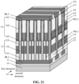
- the method further includes forming an insulating layer 17 on the second bit line BL2.
- the insulating layer 17 is used to protect the second bit line BL2.
- the disclosure also provides another semiconductor structure.
- the manufacturing process for this semiconductor structure is substantially the same as that of the semiconductor structure provided in FIGS. 5 to 22 , except for the material arrangement between the gate pillar and the semiconductor pillar.
- materials of the semiconductor pillar and the gate pillar include at least one or a combination of indium oxide, tin oxide, In-Zn oxide, Sn-Zn oxide, Al-Zn oxide, In-Ga oxide, In-Ga-Zn oxide, In-Al-Zn oxide, In-Sn-Zn oxide, Sn-Ga-Zn oxide, Al-Ga-Zn oxide, or Sn-Al-Zn oxide.
- the material of the gate pillar may be the same as that of the semiconductor pillar.
- the materials of the semiconductor pillar and the gate pillars may both be an oxide semiconductor material, such as InGaZnO 4 material.
- a transistor structure formed on the basis of the semiconductor pillar can be used as the write transistor of the semiconductor structure, while a transistor structure formed on the basis of the semiconductor layer can be used as the read transistor of the semiconductor structure. Then, one write transistor and one read transistor constitute a memory cell configured to perform a read operation of information.
- the orthographic projection of the semiconductor pillar is at least partially overlapped with that of the gate pillar on the plane of the substrate. That is, the orthographic projection of the write transistor is at least partially overlapped with that of the read transistor on the plane of the substrate. Therefore, the memory cell structure composed of one write transistor and one read transistor occupies less surface area of the substrate, which means that on the same plane area of the substrate, the semiconductor structure provided by the embodiment of the disclosure can form more memory cells. That is, the semiconductor structure of the embodiment of the disclosure can have higher integration.
- the semiconductor structure provided by the embodiment of the disclosure can form a better amount of memory cells, that is, the semiconductor structure of the embodiment of the disclosure can have a better integration.
- the material of the gate pillar is the same as that of the semiconductor pillar in the embodiment of the disclosure, that is, the material of the source/drain region of the write transistor is the same material as that of the read transistor, so that when the source/drain region of the write transistor is electrically connected to the gate of the read transistor, there is no need to worry about an increase of contact resistance caused by the effect of gate-induced gap states between the metal material and the semiconductor material, thereby effectively reducing the power consumption of the whole semiconductor structure.
- the semiconductor structure for information processing purposes may be obtained in other ways.
- the pillar includes two parts, namely a semiconductor pillar and a gate pillar, which are formed in a same process operation.
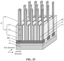
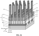
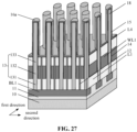
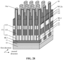
- FIGS. 24 to 29 are process flow diagrams during a method for manufacturing a semiconductor structure provided by another embodiment of the disclosure.
- the material of the substrate may be the same as or different from that in the foregoing embodiment, which is not specifically limited.
- the forming the pillar P on the substrate 10 includes the following operations.
- the pillar P is formed on substrate 10.
- the pillar P protrudes from the surface of substrate 10, and extends in the direction perpendicular to the plane of substrate 10.
- the pillar P includes a semiconductor pillar 13 and a gate pillar 18 located right on the semiconductor pillar 13.
- the method further includes the following operations.
- a plurality of first bit lines BL1 extending in a second direction are formed on the substrate 10.
- a first dielectric layer L1 is formed.
- a plurality of word line isolation structures 12 extending in a first direction are formed in the first dielectric layer L1.
- the method before forming the pillar P on the substrate 10, the method further includes the following operations.
- the first dielectric layer L1 is etched to form a plurality of first channel holes H1 used for exposing the first bit lines BL1.
- a semiconductor material layer 16a is formed.
- the semiconductor material layer 16a covers an upper surface of the first dielectric layer L1 and fills the first channel holes H1.
- the semiconductor material layer 16a is etched to form the pillars P.
- Part of each pillar P located in the first channel hole H1 is defined as the semiconductor pillar 13, and part of the each pillar P located right on the first channel hole H1 is defined as the gate pillar 18.
- the plurality of first channel holes H1 may be formed by etching the first dielectric layer L1 from top to bottom.
- the plurality of first channel hole H1 are located in the first dielectric layer L1 between two adjacent word line isolation structures 12.
- the etching the semiconductor material layer 16a to form the pillars P includes the following operations.
- the semiconductor material layer 16a is etched to remove the semiconductor material layer 16a outside regions defined by orthographic projections of the first channel holes H1 on the substrate 10, so as to remain the semiconductor material layer 16a in the first channel holes H1 and located right above the first channel holes H1, thereby forming the pillars P.
- the material of the semiconductor material layer includes at least one or a combination of indium oxide, tin oxide, In-Zn oxide, Sn-Zn oxide, Al-Zn oxide, In-Ga oxide, In-Ga-Zn oxide, In-Al-Zn oxide, In-Sn-Zn oxide, Sn-Ga-Zn oxide, Al-Ga-Zn oxide, or Sn-Al-Zn oxide.
- the material of the semiconductor material layer includes, but is not limited to, indium gallium zinc oxide (IGZO), such as the material with a chemical formula of InGaZnO 4 .
- IGZO indium gallium zinc oxide
- the material of the semiconductor material layer includes In x Ga y Zn 1-x-y O, where x is greater than or equal to 0, or less than or equal to 1, and y is greater than or equal to 0 or less than or equal to 1.
- the semiconductor pillar 13 located in the first channel hole H1 may include a first electrode 131, a first channel region 132, and a second electrode 133 distributed from bottom to top, and the first electrode 131, the first channel region 132, and the second electrode 133 have the same conductivity type.
- the first electrode 131, the first channel region 132 and the second electrode 133 of the semiconductor pillar 13 may be used as the first source/drain region, channel region and second source/drain region of a transistor respectively.
- a transistor structure based on the semiconductor pillar may be subsequently formed by forming control gate lines, such as word line structures, on part of the sidewall of the semiconductor pillar to control turn-on or turn-off of the channel region.
- control gate lines such as word line structures
- the transistor structure formed on the basis of the semiconductor pillar can be used as the write transistor of the memory.
- the formation of the first word line WL1 extending in the first direction includes the following operations.
- a plurality of third trenches T3 extending in the first direction are formed. Each of the third trenches T3 is located between two adjacent word line isolation structures 12.
- a gate dielectric layer is formed.
- the gate dielectric layer includes a first gate dielectric layer 14 surrounding part of the corresponding semiconductor pillar 13 and a second gate dielectric layer surrounding a sidewall and a top of the gate pillar 18.
- the first word line WL1 is formed in each of the third trenches T3, and surrounds part of the first gate dielectric layer 14.
- the forming the third trenches T3, includes the following operations.
- Part of the dielectric layer L1 is removed to form the plurality of third trenches T3 extending in the first direction.
- Each of the third trenches T3 is located between two adjacent word line isolation structures 12.
- the bottom of the third trench T3 is flush with the upper surface of the first electrode 131.
- the first gate dielectric layer 14 surrounds sidewalls of the first channel region 132 and the second electrode 133of the semiconductor pillar 13.
- the upper surface of the first word line WL1 is flush with the upper surface of the first channel region 132.
- a plurality of transistor structures are formed in the first dielectric layer. It is to be understood that, the plurality of transistor structures can be used as the write transistors of the memory.
- the method further includes the following operations.
- the first dielectric layer L1 is continuously filled on the first word line WL1 and in a gap between the semiconductor pillars 13, so that a top surface of the first dielectric layer L1 is flush with upper surfaces of the second electrodes 133 of the semiconductor pillars.
- a fourth dielectric layer L4 is formed.
- the fourth dielectric layer L4 covers the upper surface of the substrate 10 between adjacent gate pillars 18.
- the fourth dielectric layer covers the upper surface of the substrate between the adjacent gate pillars, an effect of electrical isolation can be realized between a structure located at the lower portion and around the semiconductor pillar and a structure located at the upper portion and around the gate pillar, thereby preventing mutual interference between the above structures.
- a semiconductor layer 16 at least surrounding a sidewall of the gate pillar 18 is formed.
- the method further includes the following operations.
- a semiconductor material layer 16a and a word line material layer WL2a are sequentially formed on the second gate dielectric layer 15.
- the semiconductor material layer 16a at least covers the second gate dielectric layer 15, while the word line material layer WL2a fills a gap between adjacent semiconductor material layers 16a.
- the semiconductor material layer 16a and the word line material layer WL2a are etched to remove part of the semiconductor material layer 16a and the word line material layer WL2a located above the word line isolation structure 12, so as to respectively form the semiconductor layer 16 and a plurality of second word lines WL2 extending in the first direction.
- the semiconductor layer 16 includes a first sub-portion 161, a second sub-portion 162, and a third sub-portion 163 connected to each other.
- the first sub-portion 161 covers a top surface of the gate pillar 18, the second sub-portion 162 covers a sidewall of the gate pillar 18, and the third sub-portion 163 partially covers an upper surface of the substrate 10 between adjacent gate pillars 18.
- the channel region of the transistor since the semiconductor layer can be used as a channel region of the transistor, and the second sub-portion thereof covers (surrounds) the sidewall of the gate pillar, the channel region of the transistor has a larger channel size compared with a structure that a channel region is only arranged on one side of a gate, thereby effectively preventing the occurrence of short channel effect by the structure provided by the embodiment of the disclosure.
- the method further includes the following operations.
- a third dielectric layer L3 is formed.
- the third dielectric layer L3 is etched to form a fourth trench T4 extending in the second direction, and used for exposing the upper surface of the semiconductor layer 16.
- a second bit line BL2 is formed in the fourth trench T4.
- the gate pillar may be used as the gate of the transistor structure
- the semiconductor layer may be used as the channel region of the transistor structure
- the second word line may be used as the source region or drain region of the read transistor
- the second bit line may be used as the drain region or the source region of the transistor structure.
- the second word line when used as the source region of the transistor structure, the second bit line is used as the drain region of the transistor structure, which is not limited thereto.
- the second word line may also be used as the drain region of the read transistor, and the second bit line may be used as the source region of the read transistor, which can be flexibly adjusted in actual operation and is not specifically limited herein.
- the second word line surrounds the second sub-portion of the semiconductor layer as the channel regions, a contact area between the second word line and the channel region is increased, which is beneficial to reduce the contact resistance between the second word line and the channel region, thereby reducing the power consumption of the transistor structure.
- the plurality of transistor structures can be used as the read transistors of the memory.
- the gate pillar and the semiconductor pillar are an integrated structure in which the gate pillar and the semiconductor pillar are electrically connected directly. That is, the channel region of the write transistor, the source/drain region of the write transistor and the gate of the read transistor are the integrated structure. That is, the source/drain region of the write transistor and the gate of the read transistor can be electrically connected directly without using other conductive wires.
- the embodiment of the disclosure can effectively shorten the charge in flow path when the charge in the write transistor is injected into the gate of the read transistor, thereby effectively improving the transmission speed and efficiency of information of the semiconductor structure.
- the structure composed of the gate pillar and the semiconductor pillar can be formed in the same process operation, which significantly reduces complexity of the process and is beneficial to an improvement of production efficiency.
- the semiconductor structure provided by the embodiments of the disclosure may be applied to a memory structure, including but not limited to, 3D dynamic random access memory (3D DRAM for short) and the like.
- 3D DRAM 3D dynamic random access memory
- the method for manufacturing a semiconductor device provided by the embodiment of the disclosure is applicable to the DRAM structure or other semiconductor devices, which is not limited herein.
- the embodiments of the method for manufacturing a semiconductor devices provided by the disclosure and the embodiments of the semiconductor device belong to the same conception.
- the technical features in the technical solutions described in the embodiment may be arbitrarily combined without conflict.
- Embodiments of the disclosure provide a semiconductor structure and a method for manufacturing the same.
- the semiconductor structure includes: a substrate; a semiconductor pillar located on the substrate and a gate pillar located on the semiconductor pillar that extend in a direction perpendicular to a plane of the substrate; a first word line extending in a first direction and surrounding the semiconductor pillar, in which the first direction is parallel to the plane of the substrate; and a semiconductor layer located above the semiconductor pillar and at least surrounding the sidewall of the gate pillar.
- the semiconductor pillar at the bottom and the semiconductor layers located thereon are longitudinally distributed.
- an area occupied by the projections of the two transistors on the substrate can be significantly reduced, compared with the case that the two transistors are tiled on the substrate, thereby effectively improving the integration level of the semiconductor structure by the embodiments of the disclosure.
Landscapes
- Engineering & Computer Science (AREA)
- Manufacturing & Machinery (AREA)
- Microelectronics & Electronic Packaging (AREA)
- Semiconductor Memories (AREA)
- Thin Film Transistor (AREA)
- Insulated Gate Type Field-Effect Transistor (AREA)
Claims (12)
- Halbleiterstruktur eines DRAM ohne Kondensator mit zwei Transistoren, umfassend:ein Substrat (10);eine Halbleitersäule (13), die sich auf dem Substrat (10) befindet, und eine Gate-Säule (18), die sich auf der Halbleitersäule (13) befindet, wobei sich die Halbleitersäule (13) und die Gate-Säule (18) beide in einer Richtung senkrecht zu einer Ebene des Substrats (10) erstrecken;eine erste Wortleitung (WL1), die sich in einer ersten Richtung parallel zur Ebene des Substrats (10) erstreckt und die Halbleitersäule (13) umgibt; undeine Halbleiterschicht (16), die sich oberhalb der Halbleitersäule (13) befindet und zumindest eine Seitenwand der Gate-Säule (18) umgibt;wobei die Halbleiterschicht (16) einen ersten Teilabschnitt (161), einen zweiten Teilabschnitt (162) und einen dritten Teilabschnitt (163) umfasst, die miteinander verbunden sind, undwobei der erste Teilabschnitt (161) eine Oberseite der Gate-Säule (18) abdeckt, der zweite Teilabschnitt (162) die Seitenwand der Gate-Säule (18) abdeckt, und der dritte Teilabschnitt (163) teilweise eine Oberseite des Substrats (10) zwischen benachbarten Gate-Säulen (18) abdeckt;wobei die Halbleiterstruktur ferner umfasst:eine zweite Wortleitung (WL2), die sich in der ersten Richtung erstreckt, ein Ende des zweiten Teilabschnitts (162) in der Nähe der Halbleitersäule (13) umgibt und eine Oberseite des dritten Teilabschnitts (163) abdeckt; undeine erste Bitleitung (BL1) und eine zweite Bitleitung (BL2), die sich in einer zweiten Richtung parallel zu der Ebene des Substrats (10) und senkrecht zu der ersten Richtung erstrecken, wobei die erste Bitleitung (BL1) unterhalb der Halbleitersäule (13) angeordnet und elektrisch mit einem unteren Abschnitt der Halbleitersäule (13) verbunden ist, während die zweite Bitleitung (BL2) oberhalb der Halbleiterschicht (16) angeordnet und elektrisch mit dem ersten Teilabschnitt (161) verbunden ist.
- Halbleiterstruktur nach Anspruch 1, wobei die Gate-Säule (18) und die Halbleitersäule (13) in einer Eins-zu-Eins-Entsprechung stehen; odereine Oberseite der Halbleitersäule (13) elektrisch mit einer Unterseite der Gate-Säule (18) verbunden ist; odereine orthographische Projektion der Halbleitersäule (13) zumindest teilweise mit einer orthographischen Projektion der Gate-Säule (18) auf der Ebene des Substrats (10) überlappt, und ein Material der Gate-Säule (18) dasselbe ist wie ein Material der Halbleitersäule (13).
- Halbleiterstruktur nach Anspruch 1, wobei die Halbleitersäule (13) eine erste Elektrode (131), einen ersten Kanalbereich (132) und eine zweite Elektrode (133) umfasst, die von unten nach oben verteilt sind, und die erste Elektrode (131), der erste Kanalbereich (132) und die zweite Elektrode (133) vom gleichen Leitfähigkeitstyp sind.
- Halbleiterstruktur nach Anspruch 3, wobei die Halbleiterstruktur ferner Folgendes umfasst:eine erste dielektrische Gate-Schicht (14), die sich zwischen der ersten Wortleitung (WL1) und der Halbleitersäule (13) befindet und den ersten Kanalbereich (132) und die zweite Elektrode (133) umgibt; undeine zweite dielektrische Gate-Schicht (15), die eine erste Teilschicht (151) und eine zweite Teilschicht (152) umfasst, die miteinander verbunden sind, wobei die erste Teilschicht (151) zwischen der Gate-Säule (18) und der Halbleiterschicht (16) angeordnet ist und eine Oberseite und die Seitenwand der Gate-Säule (18) abdeckt, während die zweite Teilschicht (152) eine Oberseite des Substrats (10) zwischen benachbarten Gate-Säulen (18) abdeckt.
- Halbleiterstruktur nach Anspruch 3, wobei die Halbleiterstruktur ferner Folgendes umfasst:eine erste dielektrische Gate-Schicht (14), die sich zwischen der ersten Wortleitung (WL1) und der Halbleitersäule (13) befindet und den ersten Kanalbereich (132) und die zweite Elektrode (133) umgibt;eine zweite dielektrische Gate-Schicht (15), die eine Oberseite und die Seitenwand der Gate-Säule (18) abdeckt; und eine vierte dielektrische Schicht (L4), die eine Oberseite des Substrats (10) zwischen benachbarten Gate-Säulen (18) abdeckt.
- Halbleiterstruktur nach Anspruch 1, wobei die Materialien der Halbleitersäule (13) und der Halbleiterschicht (16) mindestens eines oder eine Kombination von Indiumoxid, Zinnoxid, In-Zn-Oxid, Sn-Zn-Oxid, Al-Zn-Oxid, In-Ga-Oxid, In-Ga-Zn-Oxid, In-Al-Zn-Oxid, In-Sn-Zn-Oxid, Sn-Ga-Zn-Oxid, Al-Ga-Zn-Oxid oder Sn-Al-Zn-Oxid umfassen; oderdie Halbleiterstruktur ferner umfasst: eine Wortleitungsisolierungsstruktur (12), die sich in der ersten Richtung erstreckt und zwischen zwei benachbarten ersten Wortleitungen (WL1) angeordnet ist, um die benachbarten ersten Wortleitungen (WL1) zu isolieren; oderdie Halbleiterstruktur ferner umfasst: eine erste dielektrische Schicht (L1), die sich über dem Substrat (10) befindet, und eine zweite dielektrische Schicht (L2), die sich über der ersten dielektrischen Schicht (L1) befindet, wobei sich der Halbleitersäule (13) und die erste Wortleitung (WL1) in der ersten dielektrischen Schicht (L1) befinden, während sich die Gate-Säule (18), die Halbleiterschicht (16) und die zweite Wortleitung (WL2) in der zweiten dielektrischen Schicht (L2) befinden.
- Verfahren zur Herstellung einer Halbleiterstruktur eines DRAM ohne Kondensator mit zwei Transistoren, umfassend:Bereitstellen eines Substrats (10);Ausbilden einer Säule (P) auf dem Substrat (10), wobei die Säule (P) eine Halbleitersäule (13) umfasst und sich in einer Richtung senkrecht zu einer Ebene des Substrats (10) erstreckt; undAusbilden einer ersten Wortleitung (WL1), die sich in einer ersten Richtung parallel zur Ebene des Substrats (10) erstreckt und einen Teil der Säule (P) umgibt;vor dem Ausbilden der Säule auf dem Substrat (10) ferner umfassend:eine zweite Bitleitung (BL2), die sich in der zweiten Richtung erstreckt, wobei sich die zweite Bitleitung oberhalb der Halbleiterschicht (16) befindet.Ausbilden einer Isolierschicht (11) auf dem Substrat;Durchführen eines Ätzprozesses auf der Isolierschicht (11), um eine Vielzahl von ersten Gräben (T1) auszubilden, die sich in einer zweiten Richtung in der Isolierschicht (11) erstrecken, wobei die zweite Richtung parallel zur Ebene des Substrats (10) und senkrecht zur ersten Richtung ist; undFüllen der Vielzahl von ersten Gräben (T1) mit einem leitfähigen Material, um eine Vielzahl von ersten Bitleitungen (BL1) auszubilden, die sich in der zweiten Richtung erstrecken; undwobei nach dem Füllen der Vielzahl von ersten Gräben (T1) mit dem leitfähigen Material, um die Vielzahl von ersten Bitleitungen (BL1) auszubilden, die sich in der zweiten Richtung erstrecken, ferner umfassend:Ausbilden einer ersten dielektrischen Schicht (L1);Ätzen der ersten dielektrischen Schicht (L1), um eine Vielzahl von zweiten Gräben (T2) auszubilden, die sich in der ersten Richtung in der ersten dielektrischen Schicht (L1) erstrecken; undFüllen der Vielzahl von zweiten Gräben (T2) mit einem Isoliermaterial, um eine Vielzahl von Wortleitungsisolierungsstrukturen (12) auszubilden, die sich in der ersten Richtung erstrecken; undwobei das Ausbilden der Säule (P) auf dem Substrat (10) umfasst:Ätzen der ersten dielektrischen Schicht (L1), um eine Vielzahl von ersten Kanallöchern (H1) zum Freilegen der ersten Bitleitungen (BL1) auszubilden;Füllen jedes der ersten Kanallöcher (H1) mit einem Halbleitermaterial, um die Säule (P) auszubilden, wobei die Säule (P) die Halbleitersäule (13) umfasst; undwobei das Ausbilden der ersten Wortleitung (WL1), die sich in einer ersten Richtung parallel zur Ebene des Substrats (10) erstreckt und die Halbleitersäule (13) umgibt, umfasst:Ausbilden einer Vielzahl von dritten Gräben (T3), die sich in der ersten Richtung erstrecken, wobei jeder der dritten Gräben (T3) zwischen zwei benachbarten Wortleitungsisolierungsstrukturen (12) angeordnet ist;Ausbilden einer ersten dielektrischen Gate-Schicht (14) in jedem der dritten Gräben (T3), wobei die erste dielektrische Gate-Schicht (14) einen Teil der Halbleitersäule (13) umgibt; undAusbilden der ersten Wortleitung (WL1) in jedem der dritten Gräben (T3), wobei die erste Wortleitung (WL1) einen Teil der ersten dielektrischen Gate-Schicht (14) umgibt,wobei das DRAM ferner umfasst:eine auf der Halbleitersäule (13) befindliche Gate-Säule (18);eine zweite Wortleitung (WL2), die sich in der ersten Richtung erstreckt und ein Ende in der Nähe der Halbleitersäule umgibt;
- Verfahren nach Anspruch 7, nach dem Ausbilden der Wortleitung (WL1) ferner umfassend:Ausbilden einer Gate-Säule (18) direkt über der Halbleitersäule (13), wobei sich die Gate-Säule (18) in der Richtung senkrecht zur Ebene des Substrats (10) erstreckt; undAusbilden einer Halbleiterschicht (16), wobei die Halbleiterschicht (16) zumindest eine Seitenwand der Gate-Säule (18) umgibt.
- Verfahren nach Anspruch 8, wobei das Ausbilden der Gate-Säule (18) direkt über der Halbleitersäule (13) umfasst:Ausbilden und Ätzen einer zweiten dielektrischen Schicht (15), um eine Vielzahl von zweiten Kanallöchern (H2) in der zweiten dielektrischen Schicht (15) auszubilden, wobei jedes der zweiten Kanallöcher (H3) zum Freilegen einer Oberseite der Halbleitersäule (13) verwendet wird;Ausbilden der Gate-Säule (18) in jedem der zweiten Kanallöcher (H3); undwobei das Verfahren nach dem Ausbilden der Gate-Säule (18) ferner umfasst:Freilegen einer Oberseite und einer Seitenwand der Gate-Säule (18);Abscheiden einer zweiten dielektrischen Gate-Schicht (15), wobei die zweite dielektrische Gate-Schicht (15) einen Abschnitt, der die Seitenwand und eine Oberseite der Gate-Säule (18) umgibt, und einen Abschnitt, der eine Oberseite der ersten dielektrischen Schicht (L1) abdeckt, umfasst;Ausbilden einer Halbleitermaterialschicht (16a) und einer Wortleitungsmaterialschicht (WL2a) auf der zweiten dielektrischen Gate-Schicht (15) nacheinander, wobei die Halbleitermaterialschicht (16a) mit der zweiten dielektrischen Gate-Schicht (15) konform ist und die Wortleitungsmaterialschicht (WL2a) eine Lücke zwischen benachbarten Halbleitermaterialschichten (16a) füllt; undÄtzen der Halbleitermaterialschicht (16a) und der Wortleitungsmaterialschicht (WL2a), um jeweils die Halbleiterschicht (16) und eine Vielzahl von zweiten Wortleitungen (WL2) auszubilden, die sich in der ersten Richtung erstrecken.
- Verfahren nach Anspruch 8, wobei das Verfahren nach Ausbilden der Halbleiterschicht (16) ferner umfasst:Ausbilden einer dritten dielektrischen Schicht (L3);Ätzen der dritten dielektrischen Schicht (L3) zum Ausbilden eines vierten Grabens (T4), der sich in einer zweiten Richtung erstreckt und eine Oberseite der Halbleiterschicht (16) freilegt; undAusbilden einer zweiten Bit-Leitung (BL2) im vierten Graben (T4).
- Verfahren nach Anspruch 7, wobei das Ausbilden der Säule auf dem Substrat (10) umfasst:Ausbilden der Säule (P) auf dem Substrat (10), wobei die Säule (P) aus einer Oberfläche des Substrats (10) vorsteht, sich in der Richtung senkrecht zur Ebene des Substrats (10) erstreckt, die Halbleitersäule (13) und eine direkt über der Halbleitersäule (13) befindliche Gate-Säule (18) umfasst, undwobei das Verfahren nach dem Ausbilden der ersten Wortleitung (WL1) ferner umfasst: Ausbilden einer Halbleiterschicht (16), die zumindest eine Seitenwand der Gate-Säule (18) umgibt; undwobei vor dem Ausbilden der Säule (P) auf dem Substrat (10) ferner umfassend:Ausbilden einer Vielzahl von ersten Bitleitungen (BL1), die sich in einer zweiten Richtung auf dem Substrat (10) erstrecken;Ausbilden einer ersten dielektrischen Schicht (L1); undAusbilden einer Vielzahl von Wortleitungsisolierstrukturen (12), die sich in der ersten Richtung in der ersten dielektrischen Schicht (L1) erstrecken; undwobei das Ausbilden der Säule auf dem Substrat (10) umfasst:Ätzen der ersten dielektrischen Schicht (L1), um eine Vielzahl von ersten Kanallöchern (H1) zum Freilegen der ersten Bitleitungen (BL1) auszubilden;Ausbilden einer Halbleitermaterialschicht (16a), wobei die Halbleitermaterialschicht (16a) eine Oberseite der ersten dielektrischen Schicht (L1) abdeckt und das erste Kanalloch (H1) füllt; undÄtzen der Halbleitermaterialschicht (16a), um die Säule (P) auszubilden, wobei ein Abschnitt der Säule (P), der sich im ersten Kanalloch (H1) befindet, als die Halbleitersäule (13) definiert ist, und ein Abschnitt der Säule (P), der sich direkt über dem ersten Kanalloch (H1) befindet, als die Gate-Säule (18) definiert ist.
- Verfahren nach Anspruch 11, wobei das Ausbilden der ersten Wortleitungen (WL1), die sich in der ersten Richtung erstrecken, umfasst:Ausbilden einer Vielzahl von dritten Gräben (T3), die sich in der ersten Richtung erstrecken, wobei jeder der dritten Gräben (T3) zwischen zwei benachbarten Wortleitungsisolierungsstrukturen (12) angeordnet ist;Ausbilden einer dielektrischen Gate-Schicht, wobei die dielektrische Gate-Schicht eine erste dielektrische Gate-Schicht (14), die einen Teil der Halbleitersäule (13) umgibt, und eine zweite dielektrische Gate-Schicht (15), die die Seitenwand und eine Oberseite der Gate-Säule (18) umgibt, umfasst; undAusbilden der ersten Wortleitung (WL1) in jedem der dritten Gräben (T3), wobei die erste Wortleitung (WL1) einen Teil der ersten dielektrischen Gate-Schicht (14) umgibt; undwobei nach dem Ausbilden der ersten Wortleitung (WL1) ferner umfassend:Ausbilden einer Halbleitermaterialschicht (16a) und einer Wortleitungsmaterialschicht (WL2a) auf der zweiten dielektrischen Gate-Schicht (15) nacheinander, wobei die Halbleitermaterialschicht (16a) die zweite dielektrische Gate-Schicht (15) zumindest abdeckt und die Wortleitungsmaterialschicht (WL2a) eine Lücke zwischen benachbarten Halbleitermaterialschichten (16a) füllt; undÄtzen der Halbleitermaterialschicht (16a) und der Wortleitungsmaterialschicht (WL2a), um einen Teil der Halbleitermaterialschicht (16a) und der Wortleitungsmaterialschicht (WL2a), die sich oberhalb der Wortleitungsisolierungsstruktur (12) befinden, zu entfernen, um die Halbleiterschicht (16) und eine Vielzahl von zweiten Wortleitungen (WL2), die sich jeweils in der ersten Richtung erstrecken, auszubilden.
Applications Claiming Priority (2)
| Application Number | Priority Date | Filing Date | Title |
|---|---|---|---|
| CN202210933308.6A CN117580358A (zh) | 2022-08-04 | 2022-08-04 | 一种半导体结构及其制备方法 |
| PCT/CN2022/112956 WO2024026934A1 (zh) | 2022-08-04 | 2022-08-17 | 一种半导体结构及其制备方法 |
Publications (3)
| Publication Number | Publication Date |
|---|---|
| EP4344385A1 EP4344385A1 (de) | 2024-03-27 |
| EP4344385A4 EP4344385A4 (de) | 2024-07-24 |
| EP4344385B1 true EP4344385B1 (de) | 2025-06-18 |
Family
ID=87800771
Family Applications (1)
| Application Number | Title | Priority Date | Filing Date |
|---|---|---|---|
| EP22922574.3A Active EP4344385B1 (de) | 2022-08-04 | 2022-08-17 | Halbleiterstruktur und herstellungsverfahren dafür |
Country Status (7)
| Country | Link |
|---|---|
| US (1) | US12471274B2 (de) |
| EP (1) | EP4344385B1 (de) |
| JP (1) | JP7590603B2 (de) |
| KR (1) | KR102751824B1 (de) |
| CN (1) | CN117580358A (de) |
| TW (1) | TWI867580B (de) |
| WO (1) | WO2024026934A1 (de) |
Families Citing this family (3)
| Publication number | Priority date | Publication date | Assignee | Title |
|---|---|---|---|---|
| US12262523B2 (en) * | 2021-11-30 | 2025-03-25 | Changxin Memory Technologies, Inc. | Manufacturing method of semiconductor structure and semiconductor structure |
| KR20240147278A (ko) * | 2023-03-31 | 2024-10-08 | 삼성전자주식회사 | 반도체 메모리 장치 |
| KR102884518B1 (ko) | 2024-05-31 | 2025-11-12 | 서울과학기술대학교 산학협력단 | 메모리 셀 및 이를 포함하는 메모리 장치 |
Family Cites Families (17)
| Publication number | Priority date | Publication date | Assignee | Title |
|---|---|---|---|---|
| JP2655859B2 (ja) * | 1988-02-03 | 1997-09-24 | 株式会社日立製作所 | 半導体記憶装置 |
| US4939390A (en) * | 1989-01-06 | 1990-07-03 | Vitesse Semiconductor Corporation | Current-steering FET logic circuit |
| JP2003031685A (ja) | 2001-07-16 | 2003-01-31 | Sony Corp | 半導体記憶装置およびその製造方法 |
| KR101303180B1 (ko) * | 2007-11-09 | 2013-09-09 | 삼성전자주식회사 | 수직채널 트랜지스터를 구비한 반도체 메모리 소자 및 그제조 방법 |
| KR101145793B1 (ko) * | 2008-12-29 | 2012-05-16 | 에스케이하이닉스 주식회사 | 수직 채널 트랜지스터를 구비하는 반도체 소자 및 그 제조 방법 |
| US9312257B2 (en) | 2012-02-29 | 2016-04-12 | Semiconductor Energy Laboratory Co., Ltd. | Semiconductor device |
| JP6100559B2 (ja) | 2012-03-05 | 2017-03-22 | 株式会社半導体エネルギー研究所 | 半導体記憶装置 |
| KR101944535B1 (ko) * | 2012-03-28 | 2019-01-31 | 삼성전자주식회사 | 반도체 기억 소자 |
| JP6378826B2 (ja) | 2015-04-06 | 2018-08-22 | ユニサンティス エレクトロニクス シンガポール プライベート リミテッドUnisantis Electronics Singapore Pte Ltd. | Sgtを有する柱状半導体装置と、その製造方法 |
| US11653489B2 (en) * | 2019-08-28 | 2023-05-16 | Micron Technology, Inc. | Memory device having 2-transistor vertical memory cell and shield structures |
| JP2021108331A (ja) * | 2019-12-27 | 2021-07-29 | キオクシア株式会社 | 半導体記憶装置 |
| US11563007B2 (en) * | 2020-10-26 | 2023-01-24 | Nanya Technology Corporation | Semiconductor structure with vertical gate transistor |
| WO2022097251A1 (ja) * | 2020-11-06 | 2022-05-12 | ユニサンティス エレクトロニクス シンガポール プライベート リミテッド | 柱状半導体素子を用いたメモリ装置と、その製造方法 |
| CN116724354A (zh) * | 2020-12-25 | 2023-09-08 | 新加坡优尼山帝斯电子私人有限公司 | 包含半导体元件的存储器装置 |
| WO2022157929A1 (ja) | 2021-01-22 | 2022-07-28 | ユニサンティス エレクトロニクス シンガポール プライベート リミテッド | 半導体素子を用いたメモリ装置の製造方法 |
| CN114695353B (zh) | 2020-12-29 | 2023-10-13 | 长鑫存储技术有限公司 | 半导体结构及其形成方法 |
| CN113725301B (zh) | 2021-08-31 | 2024-07-02 | 上海积塔半导体有限公司 | 垂直型存储器件及其制备方法 |
-
2022
- 2022-08-04 CN CN202210933308.6A patent/CN117580358A/zh active Pending
- 2022-08-17 WO PCT/CN2022/112956 patent/WO2024026934A1/zh not_active Ceased
- 2022-08-17 JP JP2023572040A patent/JP7590603B2/ja active Active
- 2022-08-17 EP EP22922574.3A patent/EP4344385B1/de active Active
- 2022-08-17 KR KR1020237021794A patent/KR102751824B1/ko active Active
-
2023
- 2023-02-10 US US18/167,132 patent/US12471274B2/en active Active
- 2023-06-14 TW TW112122193A patent/TWI867580B/zh active
Also Published As
| Publication number | Publication date |
|---|---|
| EP4344385A4 (de) | 2024-07-24 |
| JP2024530852A (ja) | 2024-08-27 |
| EP4344385A1 (de) | 2024-03-27 |
| US12471274B2 (en) | 2025-11-11 |
| WO2024026934A1 (zh) | 2024-02-08 |
| KR102751824B1 (ko) | 2025-01-07 |
| TW202407818A (zh) | 2024-02-16 |
| TWI867580B (zh) | 2024-12-21 |
| CN117580358A (zh) | 2024-02-20 |
| KR20240020203A (ko) | 2024-02-14 |
| JP7590603B2 (ja) | 2024-11-26 |
| US20240049457A1 (en) | 2024-02-08 |
Similar Documents
| Publication | Publication Date | Title |
|---|---|---|
| EP4344385B1 (de) | Halbleiterstruktur und herstellungsverfahren dafür | |
| US10388864B2 (en) | Transistors and methods of forming transistors | |
| US11018137B2 (en) | Semiconductor memory device | |
| US7649779B2 (en) | Integrated circuits; methods for manufacturing an integrated circuit; memory modules; computing systems | |
| KR20080106116A (ko) | 집적 회로 및 그 제조 방법 | |
| CN114927477A (zh) | 一种半导体器件的制备方法、半导体器件及堆叠器件 | |
| CN115360194A (zh) | 存储器件以及其制造方法 | |
| KR20230010033A (ko) | 반도체 구조 및 제조 방법 | |
| CN208738260U (zh) | 半导体器件 | |
| CN116963498A (zh) | 半导体结构及半导体结构的制造方法 | |
| KR102704016B1 (ko) | 메모리 소자 및 그 제조 방법 | |
| US20190088488A1 (en) | Method for manufacturing semiconductor device | |
| CN120091557B (zh) | 存储器的制作方法及存储器、电子设备 | |
| CN120076312B (zh) | 半导体结构、半导体结构的制备方法及电子设备 | |
| CN119155993B (zh) | 一种半导体器件及其制造方法 | |
| US12309999B2 (en) | Semiconductor structure and manufacturing method thereof | |
| CN121604417A (zh) | 半导体器件及其制造方法、电子设备 | |
| CN119451105A (zh) | 半导体器件的制造方法及半导体器件 | |
| CN119446232A (zh) | 存储单元、存储器及数据读取方法、擦除方法、电子设备 | |
| WO2025161605A1 (zh) | 芯片及其制备方法、存储器、电子设备 | |
| KR20230142398A (ko) | 반도체 메모리 장치 및 반도체 메모리 장치 제조 방법 | |
| CN117915661A (zh) | 半导体结构及半导体结构的制造方法 |
Legal Events
| Date | Code | Title | Description |
|---|---|---|---|
| STAA | Information on the status of an ep patent application or granted ep patent |
Free format text: STATUS: UNKNOWN |
|
| STAA | Information on the status of an ep patent application or granted ep patent |
Free format text: STATUS: THE INTERNATIONAL PUBLICATION HAS BEEN MADE |
|
| PUAI | Public reference made under article 153(3) epc to a published international application that has entered the european phase |
Free format text: ORIGINAL CODE: 0009012 |
|
| STAA | Information on the status of an ep patent application or granted ep patent |
Free format text: STATUS: REQUEST FOR EXAMINATION WAS MADE |
|
| 17P | Request for examination filed |
Effective date: 20230804 |
|
| AK | Designated contracting states |
Kind code of ref document: A1 Designated state(s): AL AT BE BG CH CY CZ DE DK EE ES FI FR GB GR HR HU IE IS IT LI LT LU LV MC MK MT NL NO PL PT RO RS SE SI SK SM TR |
|
| REG | Reference to a national code |
Free format text: PREVIOUS MAIN CLASS: H10B0069000000 Ref country code: DE Ref legal event code: R079 Ref document number: 602022016250 Country of ref document: DE Free format text: PREVIOUS MAIN CLASS: H10B0069000000 Ipc: H10B0012000000 |
|
| A4 | Supplementary search report drawn up and despatched |
Effective date: 20240621 |
|
| RIC1 | Information provided on ipc code assigned before grant |
Ipc: H01L 29/786 20060101ALI20240617BHEP Ipc: H10B 12/00 20230101AFI20240617BHEP |
|
| GRAP | Despatch of communication of intention to grant a patent |
Free format text: ORIGINAL CODE: EPIDOSNIGR1 |
|
| STAA | Information on the status of an ep patent application or granted ep patent |
Free format text: STATUS: GRANT OF PATENT IS INTENDED |
|
| RIC1 | Information provided on ipc code assigned before grant |
Ipc: H10D 30/67 20250101ALI20250403BHEP Ipc: H10B 12/00 20230101AFI20250403BHEP |
|
| DAV | Request for validation of the european patent (deleted) | ||
| DAX | Request for extension of the european patent (deleted) | ||
| GRAS | Grant fee paid |
Free format text: ORIGINAL CODE: EPIDOSNIGR3 |
|
| INTG | Intention to grant announced |
Effective date: 20250411 |
|
| GRAA | (expected) grant |
Free format text: ORIGINAL CODE: 0009210 |
|
| STAA | Information on the status of an ep patent application or granted ep patent |
Free format text: STATUS: THE PATENT HAS BEEN GRANTED |
|
| AK | Designated contracting states |
Kind code of ref document: B1 Designated state(s): AL AT BE BG CH CY CZ DE DK EE ES FI FR GB GR HR HU IE IS IT LI LT LU LV MC MK MT NL NO PL PT RO RS SE SI SK SM TR |
|
| REG | Reference to a national code |
Ref country code: GB Ref legal event code: FG4D |
|
| REG | Reference to a national code |
Ref country code: CH Ref legal event code: EP |
|
| P01 | Opt-out of the competence of the unified patent court (upc) registered |
Free format text: CASE NUMBER: APP_25097/2025 Effective date: 20250527 |
|
| REG | Reference to a national code |
Ref country code: DE Ref legal event code: R096 Ref document number: 602022016250 Country of ref document: DE |
|
| REG | Reference to a national code |
Ref country code: CH Ref legal event code: EP |
|
| REG | Reference to a national code |
Ref country code: IE Ref legal event code: FG4D |
|
| PG25 | Lapsed in a contracting state [announced via postgrant information from national office to epo] |
Ref country code: FI Free format text: LAPSE BECAUSE OF FAILURE TO SUBMIT A TRANSLATION OF THE DESCRIPTION OR TO PAY THE FEE WITHIN THE PRESCRIBED TIME-LIMIT Effective date: 20250618 |
|
| PGFP | Annual fee paid to national office [announced via postgrant information from national office to epo] |
Ref country code: DE Payment date: 20250820 Year of fee payment: 4 |
|
| REG | Reference to a national code |
Ref country code: LT Ref legal event code: MG9D |
|
| PG25 | Lapsed in a contracting state [announced via postgrant information from national office to epo] |
Ref country code: NO Free format text: LAPSE BECAUSE OF FAILURE TO SUBMIT A TRANSLATION OF THE DESCRIPTION OR TO PAY THE FEE WITHIN THE PRESCRIBED TIME-LIMIT Effective date: 20250918 Ref country code: GR Free format text: LAPSE BECAUSE OF FAILURE TO SUBMIT A TRANSLATION OF THE DESCRIPTION OR TO PAY THE FEE WITHIN THE PRESCRIBED TIME-LIMIT Effective date: 20250919 |
|
| PG25 | Lapsed in a contracting state [announced via postgrant information from national office to epo] |
Ref country code: BG Free format text: LAPSE BECAUSE OF FAILURE TO SUBMIT A TRANSLATION OF THE DESCRIPTION OR TO PAY THE FEE WITHIN THE PRESCRIBED TIME-LIMIT Effective date: 20250618 |
|
| PG25 | Lapsed in a contracting state [announced via postgrant information from national office to epo] |
Ref country code: HR Free format text: LAPSE BECAUSE OF FAILURE TO SUBMIT A TRANSLATION OF THE DESCRIPTION OR TO PAY THE FEE WITHIN THE PRESCRIBED TIME-LIMIT Effective date: 20250618 |
|
| PGFP | Annual fee paid to national office [announced via postgrant information from national office to epo] |
Ref country code: AT Payment date: 20251020 Year of fee payment: 4 |
|
| PG25 | Lapsed in a contracting state [announced via postgrant information from national office to epo] |
Ref country code: RS Free format text: LAPSE BECAUSE OF FAILURE TO SUBMIT A TRANSLATION OF THE DESCRIPTION OR TO PAY THE FEE WITHIN THE PRESCRIBED TIME-LIMIT Effective date: 20250918 |
|
| REG | Reference to a national code |
Ref country code: NL Ref legal event code: MP Effective date: 20250618 |
|
| PG25 | Lapsed in a contracting state [announced via postgrant information from national office to epo] |
Ref country code: LV Free format text: LAPSE BECAUSE OF FAILURE TO SUBMIT A TRANSLATION OF THE DESCRIPTION OR TO PAY THE FEE WITHIN THE PRESCRIBED TIME-LIMIT Effective date: 20250618 |
|
| PG25 | Lapsed in a contracting state [announced via postgrant information from national office to epo] |
Ref country code: NL Free format text: LAPSE BECAUSE OF FAILURE TO SUBMIT A TRANSLATION OF THE DESCRIPTION OR TO PAY THE FEE WITHIN THE PRESCRIBED TIME-LIMIT Effective date: 20250618 |
|
| PG25 | Lapsed in a contracting state [announced via postgrant information from national office to epo] |
Ref country code: PT Free format text: LAPSE BECAUSE OF FAILURE TO SUBMIT A TRANSLATION OF THE DESCRIPTION OR TO PAY THE FEE WITHIN THE PRESCRIBED TIME-LIMIT Effective date: 20251020 |
|
| REG | Reference to a national code |
Ref country code: AT Ref legal event code: MK05 Ref document number: 1805420 Country of ref document: AT Kind code of ref document: T Effective date: 20250618 |
|
| PG25 | Lapsed in a contracting state [announced via postgrant information from national office to epo] |
Ref country code: IS Free format text: LAPSE BECAUSE OF FAILURE TO SUBMIT A TRANSLATION OF THE DESCRIPTION OR TO PAY THE FEE WITHIN THE PRESCRIBED TIME-LIMIT Effective date: 20251018 |
|
| PG25 | Lapsed in a contracting state [announced via postgrant information from national office to epo] |
Ref country code: AT Free format text: LAPSE BECAUSE OF FAILURE TO SUBMIT A TRANSLATION OF THE DESCRIPTION OR TO PAY THE FEE WITHIN THE PRESCRIBED TIME-LIMIT Effective date: 20250618 Ref country code: SM Free format text: LAPSE BECAUSE OF FAILURE TO SUBMIT A TRANSLATION OF THE DESCRIPTION OR TO PAY THE FEE WITHIN THE PRESCRIBED TIME-LIMIT Effective date: 20250618 |
|
| PG25 | Lapsed in a contracting state [announced via postgrant information from national office to epo] |
Ref country code: CZ Free format text: LAPSE BECAUSE OF FAILURE TO SUBMIT A TRANSLATION OF THE DESCRIPTION OR TO PAY THE FEE WITHIN THE PRESCRIBED TIME-LIMIT Effective date: 20250618 |
|
| PG25 | Lapsed in a contracting state [announced via postgrant information from national office to epo] |
Ref country code: PL Free format text: LAPSE BECAUSE OF FAILURE TO SUBMIT A TRANSLATION OF THE DESCRIPTION OR TO PAY THE FEE WITHIN THE PRESCRIBED TIME-LIMIT Effective date: 20250618 |
|
| PG25 | Lapsed in a contracting state [announced via postgrant information from national office to epo] |
Ref country code: EE Free format text: LAPSE BECAUSE OF FAILURE TO SUBMIT A TRANSLATION OF THE DESCRIPTION OR TO PAY THE FEE WITHIN THE PRESCRIBED TIME-LIMIT Effective date: 20250618 |
|
| PG25 | Lapsed in a contracting state [announced via postgrant information from national office to epo] |
Ref country code: SK Free format text: LAPSE BECAUSE OF FAILURE TO SUBMIT A TRANSLATION OF THE DESCRIPTION OR TO PAY THE FEE WITHIN THE PRESCRIBED TIME-LIMIT Effective date: 20250618 |
|
| PG25 | Lapsed in a contracting state [announced via postgrant information from national office to epo] |
Ref country code: ES Free format text: LAPSE BECAUSE OF FAILURE TO SUBMIT A TRANSLATION OF THE DESCRIPTION OR TO PAY THE FEE WITHIN THE PRESCRIBED TIME-LIMIT Effective date: 20250618 |
|
| PG25 | Lapsed in a contracting state [announced via postgrant information from national office to epo] |
Ref country code: RO Free format text: LAPSE BECAUSE OF FAILURE TO SUBMIT A TRANSLATION OF THE DESCRIPTION OR TO PAY THE FEE WITHIN THE PRESCRIBED TIME-LIMIT Effective date: 20250618 |
|
| REG | Reference to a national code |
Ref country code: CH Ref legal event code: H13 Free format text: ST27 STATUS EVENT CODE: U-0-0-H10-H13 (AS PROVIDED BY THE NATIONAL OFFICE) Effective date: 20260324 |
|
| PG25 | Lapsed in a contracting state [announced via postgrant information from national office to epo] |
Ref country code: MC Free format text: LAPSE BECAUSE OF FAILURE TO SUBMIT A TRANSLATION OF THE DESCRIPTION OR TO PAY THE FEE WITHIN THE PRESCRIBED TIME-LIMIT Effective date: 20250618 |
|
| PG25 | Lapsed in a contracting state [announced via postgrant information from national office to epo] |
Ref country code: DK Free format text: LAPSE BECAUSE OF FAILURE TO SUBMIT A TRANSLATION OF THE DESCRIPTION OR TO PAY THE FEE WITHIN THE PRESCRIBED TIME-LIMIT Effective date: 20250618 |
|
| PG25 | Lapsed in a contracting state [announced via postgrant information from national office to epo] |
Ref country code: LU Free format text: LAPSE BECAUSE OF NON-PAYMENT OF DUE FEES Effective date: 20250817 Ref country code: IT Free format text: LAPSE BECAUSE OF FAILURE TO SUBMIT A TRANSLATION OF THE DESCRIPTION OR TO PAY THE FEE WITHIN THE PRESCRIBED TIME-LIMIT Effective date: 20250618 |
|
| PLBE | No opposition filed within time limit |
Free format text: ORIGINAL CODE: 0009261 |
|
| STAA | Information on the status of an ep patent application or granted ep patent |
Free format text: STATUS: NO OPPOSITION FILED WITHIN TIME LIMIT |