EP4300598B1 - Solar cell contact formation using laser ablation - Google Patents
Solar cell contact formation using laser ablation Download PDFInfo
- Publication number
- EP4300598B1 EP4300598B1 EP23210934.8A EP23210934A EP4300598B1 EP 4300598 B1 EP4300598 B1 EP 4300598B1 EP 23210934 A EP23210934 A EP 23210934A EP 4300598 B1 EP4300598 B1 EP 4300598B1
- Authority
- EP
- European Patent Office
- Prior art keywords
- layer
- poly
- crystalline
- solar cell
- dielectric
- Prior art date
- Legal status (The legal status is an assumption and is not a legal conclusion. Google has not performed a legal analysis and makes no representation as to the accuracy of the status listed.)
- Active
Links
Images


Classifications
-
- H—ELECTRICITY
- H10—SEMICONDUCTOR DEVICES; ELECTRIC SOLID-STATE DEVICES NOT OTHERWISE PROVIDED FOR
- H10F—INORGANIC SEMICONDUCTOR DEVICES SENSITIVE TO INFRARED RADIATION, LIGHT, ELECTROMAGNETIC RADIATION OF SHORTER WAVELENGTH OR CORPUSCULAR RADIATION
- H10F77/00—Constructional details of devices covered by this subclass
- H10F77/93—Interconnections
- H10F77/933—Interconnections for devices having potential barriers
- H10F77/935—Interconnections for devices having potential barriers for photovoltaic devices or modules
-
- H—ELECTRICITY
- H10—SEMICONDUCTOR DEVICES; ELECTRIC SOLID-STATE DEVICES NOT OTHERWISE PROVIDED FOR
- H10F—INORGANIC SEMICONDUCTOR DEVICES SENSITIVE TO INFRARED RADIATION, LIGHT, ELECTROMAGNETIC RADIATION OF SHORTER WAVELENGTH OR CORPUSCULAR RADIATION
- H10F10/00—Individual photovoltaic cells, e.g. solar cells
- H10F10/10—Individual photovoltaic cells, e.g. solar cells having potential barriers
- H10F10/14—Photovoltaic cells having only PN homojunction potential barriers
- H10F10/146—Back-junction photovoltaic cells, e.g. having interdigitated base-emitter regions on the back side
-
- H—ELECTRICITY
- H10—SEMICONDUCTOR DEVICES; ELECTRIC SOLID-STATE DEVICES NOT OTHERWISE PROVIDED FOR
- H10F—INORGANIC SEMICONDUCTOR DEVICES SENSITIVE TO INFRARED RADIATION, LIGHT, ELECTROMAGNETIC RADIATION OF SHORTER WAVELENGTH OR CORPUSCULAR RADIATION
- H10F77/00—Constructional details of devices covered by this subclass
- H10F77/20—Electrodes
- H10F77/206—Electrodes for devices having potential barriers
- H10F77/211—Electrodes for devices having potential barriers for photovoltaic cells
- H10F77/219—Arrangements for electrodes of back-contact photovoltaic cells
-
- Y—GENERAL TAGGING OF NEW TECHNOLOGICAL DEVELOPMENTS; GENERAL TAGGING OF CROSS-SECTIONAL TECHNOLOGIES SPANNING OVER SEVERAL SECTIONS OF THE IPC; TECHNICAL SUBJECTS COVERED BY FORMER USPC CROSS-REFERENCE ART COLLECTIONS [XRACs] AND DIGESTS
- Y02—TECHNOLOGIES OR APPLICATIONS FOR MITIGATION OR ADAPTATION AGAINST CLIMATE CHANGE
- Y02E—REDUCTION OF GREENHOUSE GAS [GHG] EMISSIONS, RELATED TO ENERGY GENERATION, TRANSMISSION OR DISTRIBUTION
- Y02E10/00—Energy generation through renewable energy sources
- Y02E10/50—Photovoltaic [PV] energy
- Y02E10/546—Polycrystalline silicon PV cells
-
- Y—GENERAL TAGGING OF NEW TECHNOLOGICAL DEVELOPMENTS; GENERAL TAGGING OF CROSS-SECTIONAL TECHNOLOGIES SPANNING OVER SEVERAL SECTIONS OF THE IPC; TECHNICAL SUBJECTS COVERED BY FORMER USPC CROSS-REFERENCE ART COLLECTIONS [XRACs] AND DIGESTS
- Y02—TECHNOLOGIES OR APPLICATIONS FOR MITIGATION OR ADAPTATION AGAINST CLIMATE CHANGE
- Y02E—REDUCTION OF GREENHOUSE GAS [GHG] EMISSIONS, RELATED TO ENERGY GENERATION, TRANSMISSION OR DISTRIBUTION
- Y02E10/00—Energy generation through renewable energy sources
- Y02E10/50—Photovoltaic [PV] energy
- Y02E10/547—Monocrystalline silicon PV cells
Definitions
- Embodiments of the present invention are in the field of renewable energy and, in particular, the formation of single-step damage free solar cell contact openings using a laser.
- Metal contact formation to electrically active areas in semi-conductor and solar industries often involves a removal of dielectric material(s) (e.g., an oxide or nitride material), which may exist to electrically isolate or passivate certain active areas.
- dielectric material(s) e.g., an oxide or nitride material
- Commonly practiced methods may require several process operations, such as deposition of a mask layer, selective etching of dielectric layer(s), and removal of a mask, or laser with subsequent etch or anneal.
- WO 2009/094575 A2 discloses a buried insulator isolation for solar cell contacts.
- a buried oxide is provided under the emitter of a polysilicon emitter solar cell. Holes in the oxide provide contact areas, increasing the current density to enhance efficiency. The oxide isolates the contacts from the substrate.
- US 2009/239331 Al discloses methods for forming a photovoltaic cell electrode. The methods involve creating contact openings in the passivation layer, selectively plating contact metal, depositing a metal-containing material (such as lead-free silver paste), and firing the deposited contact metal and the deposited metal containing material.
- a metal-containing material such as lead-free silver paste
- a solar cell as defined in claim 1. Preferred embodiments are set forth in the dependent claims. According to an aspect, a solar cell comprises:
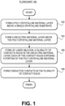
- a method includes forming a poly-crystalline material layer above a single-crystalline substrate.
- a dielectric material stack is formed above the poly-crystalline material layer.
- a plurality of contacts holes is formed in the dielectric material stack by laser ablation, each of the contact holes exposing a portion of the poly-crystalline material layer.
- Conductive contacts are formed in the plurality of contact holes.
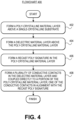
- a method includes forming a poly-crystalline material layer above a single-crystalline substrate.
- a dielectric material stack is formed above the poly-crystalline material layer.
- a recast poly signature is formed in the poly-crystalline material layer.
- a plurality of conductive contacts is formed in the dielectric material stack and coupled directly to a portion of the poly-crystalline material layer, one of the conductive contacts in alignment with the recast poly signature. It is to be understood that embodiments of the present invention need not be limited to the formation of back-side contacts, but could be used to form front-side contacts instead or as well.
- a back-contact solar cell includes a poly-crystalline material layer disposed above a single-crystalline substrate.
- a dielectric material stack is disposed above the poly-crystalline material layer.
- a plurality of conductive contacts is disposed in the dielectric material stack and coupled directly to a portion of the poly-crystalline material layer.
- a recast poly signature is disposed in the poly-crystalline material layer and in alignment with one of the plurality of conductive contacts.
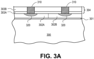
- the method of fabricating a back-contact solar cell also includes forming a dielectric material stack 204 above poly-crystalline material layer 202.
- forming dielectric material stack 204 above poly-crystalline material layer 202 includes forming a silicon dioxide layer 203A directly on poly-crystalline material layer 202, and forming a silicon nitride layer 203B directly on silicon dioxide layer 203A.
- forming silicon dioxide layer 203A includes forming to a thickness sufficiently low to not reflect back laser energy during a laser ablation process.
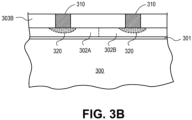
- forming silicon dioxide layer 203A includes forming to a thickness sufficiently high to act as an ablation stop layer during a laser ablation process. In one embodiment, forming silicon dioxide layer 203A includes forming the layer to have a thickness approximately in the range of 1 - 50 nanometers. In a specific embodiment, forming silicon dioxide layer 203A includes forming the layer to have a thickness approximately in the range of 5 - 15 nanometers. However, in another embodiment, there is no layer 203A in the dielectric stack and only a silicon nitride layer 203B is included, as depicted in Figure 2B' .
- the method of fabricating a back-contact solar cell also includes forming conductive contacts 210 in the plurality of contact holes 208.
Landscapes
- Photovoltaic Devices (AREA)
- Life Sciences & Earth Sciences (AREA)
- Engineering & Computer Science (AREA)
- Sustainable Development (AREA)
- Sustainable Energy (AREA)
Applications Claiming Priority (5)
| Application Number | Priority Date | Filing Date | Title |
|---|---|---|---|
| US26565209P | 2009-12-01 | 2009-12-01 | |
| US12/895,437 US8324015B2 (en) | 2009-12-01 | 2010-09-30 | Solar cell contact formation using laser ablation |
| EP20165212.0A EP3723141B1 (en) | 2009-12-01 | 2010-10-01 | Solar cell contact formation using laser ablation |
| EP10834898.8A EP2507844B1 (en) | 2009-12-01 | 2010-10-01 | Solar cell contact formation using laser ablation |
| PCT/US2010/051178 WO2011068590A2 (en) | 2009-12-01 | 2010-10-01 | Solar cell contact formation using laser ablation |
Related Parent Applications (2)
| Application Number | Title | Priority Date | Filing Date |
|---|---|---|---|
| EP20165212.0A Division EP3723141B1 (en) | 2009-12-01 | 2010-10-01 | Solar cell contact formation using laser ablation |
| EP10834898.8A Division EP2507844B1 (en) | 2009-12-01 | 2010-10-01 | Solar cell contact formation using laser ablation |
Publications (3)
| Publication Number | Publication Date |
|---|---|
| EP4300598A2 EP4300598A2 (en) | 2024-01-03 |
| EP4300598A3 EP4300598A3 (en) | 2024-03-27 |
| EP4300598B1 true EP4300598B1 (en) | 2025-04-09 |
Family
ID=44067930
Family Applications (3)
| Application Number | Title | Priority Date | Filing Date |
|---|---|---|---|
| EP23210934.8A Active EP4300598B1 (en) | 2009-12-01 | 2010-10-01 | Solar cell contact formation using laser ablation |
| EP20165212.0A Active EP3723141B1 (en) | 2009-12-01 | 2010-10-01 | Solar cell contact formation using laser ablation |
| EP10834898.8A Active EP2507844B1 (en) | 2009-12-01 | 2010-10-01 | Solar cell contact formation using laser ablation |
Family Applications After (2)
| Application Number | Title | Priority Date | Filing Date |
|---|---|---|---|
| EP20165212.0A Active EP3723141B1 (en) | 2009-12-01 | 2010-10-01 | Solar cell contact formation using laser ablation |
| EP10834898.8A Active EP2507844B1 (en) | 2009-12-01 | 2010-10-01 | Solar cell contact formation using laser ablation |
Country Status (7)
| Country | Link |
|---|---|
| US (6) | US8324015B2 (enExample) |
| EP (3) | EP4300598B1 (enExample) |
| JP (3) | JP5726892B2 (enExample) |
| CN (2) | CN107134498B (enExample) |
| MY (1) | MY155779A (enExample) |
| PH (1) | PH12012500956A1 (enExample) |
| WO (1) | WO2011068590A2 (enExample) |
Families Citing this family (39)
| Publication number | Priority date | Publication date | Assignee | Title |
|---|---|---|---|---|
| US20170005206A1 (en) * | 2007-10-06 | 2017-01-05 | Solexel, Inc. | Patterning of silicon oxide layers using pulsed laser ablation |
| US8242354B2 (en) * | 2008-12-04 | 2012-08-14 | Sunpower Corporation | Backside contact solar cell with formed polysilicon doped regions |
| US8324015B2 (en) * | 2009-12-01 | 2012-12-04 | Sunpower Corporation | Solar cell contact formation using laser ablation |
| WO2012092301A2 (en) * | 2010-12-29 | 2012-07-05 | Intevac, Inc. | Method and apparatus for masking substrates for deposition |
| US8658458B2 (en) * | 2011-06-15 | 2014-02-25 | Varian Semiconductor Equipment Associates, Inc. | Patterned doping for polysilicon emitter solar cells |
| US8692111B2 (en) * | 2011-08-23 | 2014-04-08 | Sunpower Corporation | High throughput laser ablation processes and structures for forming contact holes in solar cells |
| EP2579317A1 (en) * | 2011-10-07 | 2013-04-10 | Total SA | Method of manufacturing a solar cell with local back contacts |
| CN103890978A (zh) * | 2011-10-28 | 2014-06-25 | 应用材料公司 | 用于太阳能电池制造的背接点通孔形成工艺 |
| US20130199606A1 (en) * | 2012-02-06 | 2013-08-08 | Applied Materials, Inc. | Methods of manufacturing back surface field and metallized contacts on a solar cell device |
| DE102012205966A1 (de) * | 2012-04-12 | 2013-10-17 | Robert Bosch Gmbh | Verfahren zur Herstellung eines Dünnschicht-Solarmoduls |
| WO2014144967A1 (en) * | 2013-03-15 | 2014-09-18 | Sunpower Corporation | Reduced contact resistance and improved lifetime of solar cells |
| CN109599450B (zh) | 2013-04-03 | 2026-07-10 | 晶澳太阳能有限公司 | 太阳能电池 |
| KR101613843B1 (ko) * | 2013-04-23 | 2016-04-20 | 엘지전자 주식회사 | 태양 전지 및 이의 제조 방법 |
| US9768343B2 (en) * | 2013-04-29 | 2017-09-19 | OB Realty, LLC. | Damage free laser patterning of transparent layers for forming doped regions on a solar cell substrate |
| KR102045001B1 (ko) * | 2013-06-05 | 2019-12-02 | 엘지전자 주식회사 | 태양 전지 및 이의 제조 방법 |
| KR101622089B1 (ko) * | 2013-07-05 | 2016-05-18 | 엘지전자 주식회사 | 태양 전지 및 이의 제조 방법 |
| KR101620431B1 (ko) * | 2014-01-29 | 2016-05-12 | 엘지전자 주식회사 | 태양 전지 및 이의 제조 방법 |
| KR101569415B1 (ko) | 2014-06-09 | 2015-11-16 | 엘지전자 주식회사 | 태양 전지의 제조 방법 |
| KR102219804B1 (ko) | 2014-11-04 | 2021-02-24 | 엘지전자 주식회사 | 태양 전지 및 그의 제조 방법 |
| JP6219913B2 (ja) | 2014-11-28 | 2017-10-25 | エルジー エレクトロニクス インコーポレイティド | 太陽電池及びその製造方法 |
| US10535790B2 (en) * | 2015-06-25 | 2020-01-14 | Sunpower Corporation | One-dimensional metallization for solar cells |
| KR102272433B1 (ko) | 2015-06-30 | 2021-07-05 | 엘지전자 주식회사 | 태양 전지 및 이의 제조 방법 |
| KR102600379B1 (ko) | 2015-12-21 | 2023-11-10 | 상라오 징코 솔라 테크놀러지 디벨롭먼트 컴퍼니, 리미티드 | 태양 전지와 그 제조 방법 |
| KR102526398B1 (ko) * | 2016-01-12 | 2023-04-27 | 상라오 징코 솔라 테크놀러지 디벨롭먼트 컴퍼니, 리미티드 | 태양 전지 및 이의 제조 방법 |
| JP2017143267A (ja) * | 2016-02-12 | 2017-08-17 | エルジー エレクトロニクス インコーポレイティド | 太陽電池及びその製造方法 |
| USD822890S1 (en) | 2016-09-07 | 2018-07-10 | Felxtronics Ap, Llc | Lighting apparatus |
| US10775030B2 (en) | 2017-05-05 | 2020-09-15 | Flex Ltd. | Light fixture device including rotatable light modules |
| USD877964S1 (en) | 2017-08-09 | 2020-03-10 | Flex Ltd. | Lighting module |
| USD862777S1 (en) | 2017-08-09 | 2019-10-08 | Flex Ltd. | Lighting module wide distribution lens |
| USD846793S1 (en) | 2017-08-09 | 2019-04-23 | Flex Ltd. | Lighting module locking mechanism |
| USD872319S1 (en) | 2017-08-09 | 2020-01-07 | Flex Ltd. | Lighting module LED light board |
| USD832494S1 (en) | 2017-08-09 | 2018-10-30 | Flex Ltd. | Lighting module heatsink |
| USD833061S1 (en) | 2017-08-09 | 2018-11-06 | Flex Ltd. | Lighting module locking endcap |
| USD832495S1 (en) | 2017-08-18 | 2018-10-30 | Flex Ltd. | Lighting module locking mechanism |
| USD862778S1 (en) | 2017-08-22 | 2019-10-08 | Flex Ltd | Lighting module lens |
| USD888323S1 (en) | 2017-09-07 | 2020-06-23 | Flex Ltd | Lighting module wire guard |
| KR102350960B1 (ko) * | 2019-04-25 | 2022-01-14 | 엘지전자 주식회사 | 태양전지의 제조 방법 |
| US12329704B2 (en) | 2021-08-23 | 2025-06-17 | Medline Industries, Lp | Absorbent repositioning pad and method |
| CN117059681B (zh) | 2023-10-09 | 2024-03-29 | 晶科能源(海宁)有限公司 | 太阳能电池及其制造方法、光伏组件 |
Family Cites Families (57)
| Publication number | Priority date | Publication date | Assignee | Title |
|---|---|---|---|---|
| US4626613A (en) | 1983-12-23 | 1986-12-02 | Unisearch Limited | Laser grooved solar cell |
| US4900695A (en) * | 1986-12-17 | 1990-02-13 | Hitachi, Ltd. | Semiconductor integrated circuit device and process for producing the same |
| JP2706113B2 (ja) | 1988-11-25 | 1998-01-28 | 工業技術院長 | 光電変換素子 |
| US5053083A (en) * | 1989-05-08 | 1991-10-01 | The Board Of Trustees Of The Leland Stanford Junior University | Bilevel contact solar cells |
| US5011565A (en) | 1989-12-06 | 1991-04-30 | Mobil Solar Energy Corporation | Dotted contact solar cell and method of making same |
| JP2798769B2 (ja) | 1990-02-22 | 1998-09-17 | 三洋電機株式会社 | 薄膜トランジスタの製造方法 |
| US5258077A (en) | 1991-09-13 | 1993-11-02 | Solec International, Inc. | High efficiency silicon solar cells and method of fabrication |
| US5738731A (en) * | 1993-11-19 | 1998-04-14 | Mega Chips Corporation | Photovoltaic device |
| US5456763A (en) | 1994-03-29 | 1995-10-10 | The Regents Of The University Of California | Solar cells utilizing pulsed-energy crystallized microcrystalline/polycrystalline silicon |
| JP3193287B2 (ja) * | 1996-02-28 | 2001-07-30 | シャープ株式会社 | 太陽電池 |
| JPH10229211A (ja) * | 1997-02-18 | 1998-08-25 | Hitachi Ltd | 光電変換装置およびその製造方法 |
| DE19741832A1 (de) | 1997-09-23 | 1999-03-25 | Inst Solarenergieforschung | Verfahren zur Herstellung einer Solarzelle und Solarzelle |
| US6126565A (en) | 1999-03-31 | 2000-10-03 | Dana Corporation | Method for controlling flow of lubrication in axle assembly and axle assembly with selectively adjustable drain-back spacer |
| DE10046170A1 (de) | 2000-09-19 | 2002-04-04 | Fraunhofer Ges Forschung | Verfahren zur Herstellung eines Halbleiter-Metallkontaktes durch eine dielektrische Schicht |
| JP2003298078A (ja) * | 2002-03-29 | 2003-10-17 | Ebara Corp | 光起電力素子 |
| US7388147B2 (en) * | 2003-04-10 | 2008-06-17 | Sunpower Corporation | Metal contact structure for solar cell and method of manufacture |
| US20050172996A1 (en) * | 2004-02-05 | 2005-08-11 | Advent Solar, Inc. | Contact fabrication of emitter wrap-through back contact silicon solar cells |
| US8049669B2 (en) * | 2004-03-26 | 2011-11-01 | Semiconductor Energy Laboratory Co., Ltd. | Semiconductor device comprising circuit between first and second conducting wires |
| DE102004050269A1 (de) | 2004-10-14 | 2006-04-20 | Institut Für Solarenergieforschung Gmbh | Verfahren zur Kontakttrennung elektrisch leitfähiger Schichten auf rückkontaktierten Solarzellen und Solarzelle |
| US20060130891A1 (en) * | 2004-10-29 | 2006-06-22 | Carlson David E | Back-contact photovoltaic cells |
| US8129822B2 (en) | 2006-10-09 | 2012-03-06 | Solexel, Inc. | Template for three-dimensional thin-film solar cell manufacturing and methods of use |
| US8399331B2 (en) | 2007-10-06 | 2013-03-19 | Solexel | Laser processing for high-efficiency thin crystalline silicon solar cell fabrication |
| US8420435B2 (en) | 2009-05-05 | 2013-04-16 | Solexel, Inc. | Ion implantation fabrication process for thin-film crystalline silicon solar cells |
| FR2880989B1 (fr) * | 2005-01-20 | 2007-03-09 | Commissariat Energie Atomique | Dispositif semi-conducteur a heterojonctions et a structure inter-digitee |
| EP1763086A1 (en) * | 2005-09-09 | 2007-03-14 | Interuniversitair Micro-Elektronica Centrum | Photovoltaic cell with thick silicon oxide and silicon nitride passivation and fabrication method |
| US7279362B2 (en) * | 2005-03-31 | 2007-10-09 | Intel Corporation | Semiconductor wafer coat layers and methods therefor |
| DE102005040871A1 (de) * | 2005-04-16 | 2006-10-19 | Institut Für Solarenergieforschung Gmbh | Rückkontaktierte Solarzelle und Verfahren zu deren Herstellung |
| US7468485B1 (en) * | 2005-08-11 | 2008-12-23 | Sunpower Corporation | Back side contact solar cell with doped polysilicon regions |
| US20070137692A1 (en) | 2005-12-16 | 2007-06-21 | Bp Corporation North America Inc. | Back-Contact Photovoltaic Cells |
| US8084684B2 (en) | 2006-10-09 | 2011-12-27 | Solexel, Inc. | Three-dimensional thin-film solar cells |
| JP2009152222A (ja) * | 2006-10-27 | 2009-07-09 | Kyocera Corp | 太陽電池素子の製造方法 |
| US7705237B2 (en) * | 2006-11-27 | 2010-04-27 | Sunpower Corporation | Solar cell having silicon nano-particle emitter |
| EP2122691A4 (en) * | 2007-02-16 | 2011-02-16 | Nanogram Corp | SOLAR CELL STRUCTURES, PV MODULES AND CORRESPONDING METHODS |
| EP2135292A2 (en) * | 2007-03-16 | 2009-12-23 | BP Corporation North America Inc. | Solar cells |
| JP2008283023A (ja) | 2007-05-11 | 2008-11-20 | Mitsubishi Heavy Ind Ltd | 光電変換装置の製造方法 |
| JP5230153B2 (ja) | 2007-09-18 | 2013-07-10 | 三菱重工業株式会社 | 光電変換装置の製造方法 |
| US7960644B2 (en) * | 2007-11-09 | 2011-06-14 | Sunpreme, Ltd. | Low-cost multi-junction solar cells and methods for their production |
| US8198528B2 (en) * | 2007-12-14 | 2012-06-12 | Sunpower Corporation | Anti-reflective coating with high optical absorption layer for backside contact solar cells |
| US7820540B2 (en) * | 2007-12-21 | 2010-10-26 | Palo Alto Research Center Incorporated | Metallization contact structures and methods for forming multiple-layer electrode structures for silicon solar cells |
| WO2009094575A2 (en) * | 2008-01-24 | 2009-07-30 | Applied Materials, Inc. | Buried insulator isolation for solar cell contacts |
| US20090188553A1 (en) * | 2008-01-25 | 2009-07-30 | Emat Technology, Llc | Methods of fabricating solar-cell structures and resulting solar-cell structures |
| KR100864062B1 (ko) * | 2008-02-22 | 2008-10-16 | 한국철강 주식회사 | 태양전지 모듈 패터닝 장치 |
| KR101155343B1 (ko) * | 2008-02-25 | 2012-06-11 | 엘지전자 주식회사 | 백 콘택 태양전지의 제조 방법 |
| US7833808B2 (en) * | 2008-03-24 | 2010-11-16 | Palo Alto Research Center Incorporated | Methods for forming multiple-layer electrode structures for silicon photovoltaic cells |
| KR20100136542A (ko) * | 2008-04-09 | 2010-12-28 | 어플라이드 머티어리얼스, 인코포레이티드 | 폴리실리콘 에미터 태양전지용의 단순화된 후면 접촉부 |
| US20090260685A1 (en) * | 2008-04-17 | 2009-10-22 | Daeyong Lee | Solar cell and method of manufacturing the same |
| US7851698B2 (en) * | 2008-06-12 | 2010-12-14 | Sunpower Corporation | Trench process and structure for backside contact solar cells with polysilicon doped regions |
| US20100071765A1 (en) * | 2008-09-19 | 2010-03-25 | Peter Cousins | Method for fabricating a solar cell using a direct-pattern pin-hole-free masking layer |
| US8242354B2 (en) | 2008-12-04 | 2012-08-14 | Sunpower Corporation | Backside contact solar cell with formed polysilicon doped regions |
| CN101447518A (zh) * | 2008-12-31 | 2009-06-03 | 江苏艾德太阳能科技有限公司 | 一种背点接触异质结太阳能电池及其制造方法 |
| US8940572B2 (en) | 2009-04-21 | 2015-01-27 | Tetrasun, Inc. | Method for forming structures in a solar cell |
| JP5643294B2 (ja) | 2009-04-22 | 2014-12-17 | テトラサン インコーポレイテッド | 太陽電池内の機能膜の局所的レーザ転化による局所的金属接触子 |
| US8324015B2 (en) * | 2009-12-01 | 2012-12-04 | Sunpower Corporation | Solar cell contact formation using laser ablation |
| CN103890978A (zh) | 2011-10-28 | 2014-06-25 | 应用材料公司 | 用于太阳能电池制造的背接点通孔形成工艺 |
| DE102012205966A1 (de) | 2012-04-12 | 2013-10-17 | Robert Bosch Gmbh | Verfahren zur Herstellung eines Dünnschicht-Solarmoduls |
| WO2014144967A1 (en) | 2013-03-15 | 2014-09-18 | Sunpower Corporation | Reduced contact resistance and improved lifetime of solar cells |
| US9768343B2 (en) | 2013-04-29 | 2017-09-19 | OB Realty, LLC. | Damage free laser patterning of transparent layers for forming doped regions on a solar cell substrate |
-
2010
- 2010-09-30 US US12/895,437 patent/US8324015B2/en active Active
- 2010-10-01 EP EP23210934.8A patent/EP4300598B1/en active Active
- 2010-10-01 WO PCT/US2010/051178 patent/WO2011068590A2/en not_active Ceased
- 2010-10-01 CN CN201710165852.XA patent/CN107134498B/zh active Active
- 2010-10-01 EP EP20165212.0A patent/EP3723141B1/en active Active
- 2010-10-01 MY MYPI2012002257A patent/MY155779A/en unknown
- 2010-10-01 EP EP10834898.8A patent/EP2507844B1/en active Active
- 2010-10-01 PH PH1/2012/500956A patent/PH12012500956A1/en unknown
- 2010-10-01 CN CN201080054693.2A patent/CN102640300B/zh active Active
- 2010-10-01 JP JP2012542005A patent/JP5726892B2/ja active Active
-
2012
- 2012-11-05 US US13/669,147 patent/US8785236B2/en active Active
-
2014
- 2014-07-17 US US14/334,401 patent/US9087939B2/en active Active
-
2015
- 2015-04-01 JP JP2015075493A patent/JP6089058B2/ja active Active
- 2015-07-07 US US14/793,356 patent/US10211349B2/en active Active
-
2017
- 2017-02-06 JP JP2017019684A patent/JP6648358B2/ja active Active
-
2019
- 2019-02-14 US US16/276,381 patent/US11152518B2/en active Active
-
2021
- 2021-10-12 US US17/498,979 patent/US12191404B2/en active Active
Also Published As
Similar Documents
| Publication | Publication Date | Title |
|---|---|---|
| US12191404B2 (en) | Solar cell having conductive contacts in alignment with recast signatures | |
| US8637340B2 (en) | Patterning of silicon oxide layers using pulsed laser ablation | |
| EP2676302B1 (en) | Process and structures for fabrication of solar cells | |
| US9455362B2 (en) | Laser irradiation aluminum doping for monocrystalline silicon substrates | |
| US20160093763A1 (en) | Damage free laser patterning of transparent layers for forming doped regions on a solar cell substrate | |
| KR101384853B1 (ko) | 광기전 태양 전지의 레이저 가공 방법 | |
| US20120225515A1 (en) | Laser doping techniques for high-efficiency crystalline semiconductor solar cells | |
| US20130164883A1 (en) | Laser annealing applications in high-efficiency solar cells | |
| EP2748858A1 (en) | High throughput laser ablation processes and structures for forming contact holes in solar cells | |
| US20170005206A1 (en) | Patterning of silicon oxide layers using pulsed laser ablation | |
| EP2819181A1 (en) | Laser annealing applications in high-efficiency solar cells |
Legal Events
| Date | Code | Title | Description |
|---|---|---|---|
| PUAI | Public reference made under article 153(3) epc to a published international application that has entered the european phase |
Free format text: ORIGINAL CODE: 0009012 |
|
| STAA | Information on the status of an ep patent application or granted ep patent |
Free format text: STATUS: THE APPLICATION HAS BEEN PUBLISHED |
|
| AC | Divisional application: reference to earlier application |
Ref document number: 2507844 Country of ref document: EP Kind code of ref document: P Ref document number: 3723141 Country of ref document: EP Kind code of ref document: P |
|
| AK | Designated contracting states |
Kind code of ref document: A2 Designated state(s): AL AT BE BG CH CY CZ DE DK EE ES FI FR GB GR HR HU IE IS IT LI LT LU LV MC MK MT NL NO PL PT RO RS SE SI SK SM TR |
|
| REG | Reference to a national code |
Ref country code: DE Ref legal event code: R079 Ref document number: 602010069721 Country of ref document: DE Free format text: PREVIOUS MAIN CLASS: H01L0031068000 Ipc: H01L0031042000 Ref country code: DE Ref legal event code: R079 Free format text: PREVIOUS MAIN CLASS: H01L0031068000 Ipc: H01L0031042000 |
|
| PUAL | Search report despatched |
Free format text: ORIGINAL CODE: 0009013 |
|
| AK | Designated contracting states |
Kind code of ref document: A3 Designated state(s): AL AT BE BG CH CY CZ DE DK EE ES FI FR GB GR HR HU IE IS IT LI LT LU LV MC MK MT NL NO PL PT RO RS SE SI SK SM TR |
|
| RIC1 | Information provided on ipc code assigned before grant |
Ipc: H01L 31/068 20120101ALI20240216BHEP Ipc: H01L 31/0224 20060101ALI20240216BHEP Ipc: H01L 31/18 20060101ALI20240216BHEP Ipc: H01L 31/042 20140101AFI20240216BHEP |
|
| STAA | Information on the status of an ep patent application or granted ep patent |
Free format text: STATUS: REQUEST FOR EXAMINATION WAS MADE |
|
| 17P | Request for examination filed |
Effective date: 20240925 |
|
| RBV | Designated contracting states (corrected) |
Designated state(s): AL AT BE BG CH CY CZ DE DK EE ES FI FR GB GR HR HU IE IS IT LI LT LU LV MC MK MT NL NO PL PT RO RS SE SI SK SM TR |
|
| GRAP | Despatch of communication of intention to grant a patent |
Free format text: ORIGINAL CODE: EPIDOSNIGR1 |
|
| STAA | Information on the status of an ep patent application or granted ep patent |
Free format text: STATUS: GRANT OF PATENT IS INTENDED |
|
| RIC1 | Information provided on ipc code assigned before grant |
Ipc: H01L 31/068 20120101ALI20241021BHEP Ipc: H01L 31/0224 20060101ALI20241021BHEP Ipc: H01L 31/18 20060101ALI20241021BHEP Ipc: H01L 31/042 20140101AFI20241021BHEP |
|
| INTG | Intention to grant announced |
Effective date: 20241105 |
|
| GRAS | Grant fee paid |
Free format text: ORIGINAL CODE: EPIDOSNIGR3 |
|
| GRAA | (expected) grant |
Free format text: ORIGINAL CODE: 0009210 |
|
| STAA | Information on the status of an ep patent application or granted ep patent |
Free format text: STATUS: THE PATENT HAS BEEN GRANTED |
|
| AC | Divisional application: reference to earlier application |
Ref document number: 2507844 Country of ref document: EP Kind code of ref document: P Ref document number: 3723141 Country of ref document: EP Kind code of ref document: P |
|
| AK | Designated contracting states |
Kind code of ref document: B1 Designated state(s): AL AT BE BG CH CY CZ DE DK EE ES FI FR GB GR HR HU IE IS IT LI LT LU LV MC MK MT NL NO PL PT RO RS SE SI SK SM TR |
|
| REG | Reference to a national code |
Ref country code: GB Ref legal event code: FG4D |
|
| REG | Reference to a national code |
Ref country code: DE Ref legal event code: R096 Ref document number: 602010069721 Country of ref document: DE |
|
| REG | Reference to a national code |
Ref country code: IE Ref legal event code: FG4D |
|
| REG | Reference to a national code |
Ref country code: NL Ref legal event code: FP |
|
| REG | Reference to a national code |
Ref country code: AT Ref legal event code: MK05 Ref document number: 1784383 Country of ref document: AT Kind code of ref document: T Effective date: 20250409 |
|
| PG25 | Lapsed in a contracting state [announced via postgrant information from national office to epo] |
Ref country code: FI Free format text: LAPSE BECAUSE OF FAILURE TO SUBMIT A TRANSLATION OF THE DESCRIPTION OR TO PAY THE FEE WITHIN THE PRESCRIBED TIME-LIMIT Effective date: 20250409 Ref country code: ES Free format text: LAPSE BECAUSE OF FAILURE TO SUBMIT A TRANSLATION OF THE DESCRIPTION OR TO PAY THE FEE WITHIN THE PRESCRIBED TIME-LIMIT Effective date: 20250409 Ref country code: PT Free format text: LAPSE BECAUSE OF FAILURE TO SUBMIT A TRANSLATION OF THE DESCRIPTION OR TO PAY THE FEE WITHIN THE PRESCRIBED TIME-LIMIT Effective date: 20250811 |
|
| REG | Reference to a national code |
Ref country code: LT Ref legal event code: MG9D |
|
| PG25 | Lapsed in a contracting state [announced via postgrant information from national office to epo] |
Ref country code: NO Free format text: LAPSE BECAUSE OF FAILURE TO SUBMIT A TRANSLATION OF THE DESCRIPTION OR TO PAY THE FEE WITHIN THE PRESCRIBED TIME-LIMIT Effective date: 20250709 Ref country code: GR Free format text: LAPSE BECAUSE OF FAILURE TO SUBMIT A TRANSLATION OF THE DESCRIPTION OR TO PAY THE FEE WITHIN THE PRESCRIBED TIME-LIMIT Effective date: 20250710 |
|
| PG25 | Lapsed in a contracting state [announced via postgrant information from national office to epo] |
Ref country code: PL Free format text: LAPSE BECAUSE OF FAILURE TO SUBMIT A TRANSLATION OF THE DESCRIPTION OR TO PAY THE FEE WITHIN THE PRESCRIBED TIME-LIMIT Effective date: 20250409 |
|
| PG25 | Lapsed in a contracting state [announced via postgrant information from national office to epo] |
Ref country code: BG Free format text: LAPSE BECAUSE OF FAILURE TO SUBMIT A TRANSLATION OF THE DESCRIPTION OR TO PAY THE FEE WITHIN THE PRESCRIBED TIME-LIMIT Effective date: 20250409 |
|
| PG25 | Lapsed in a contracting state [announced via postgrant information from national office to epo] |
Ref country code: HR Free format text: LAPSE BECAUSE OF FAILURE TO SUBMIT A TRANSLATION OF THE DESCRIPTION OR TO PAY THE FEE WITHIN THE PRESCRIBED TIME-LIMIT Effective date: 20250409 |
|
| PG25 | Lapsed in a contracting state [announced via postgrant information from national office to epo] |
Ref country code: AT Free format text: LAPSE BECAUSE OF FAILURE TO SUBMIT A TRANSLATION OF THE DESCRIPTION OR TO PAY THE FEE WITHIN THE PRESCRIBED TIME-LIMIT Effective date: 20250409 |
|
| PG25 | Lapsed in a contracting state [announced via postgrant information from national office to epo] |
Ref country code: IS Free format text: LAPSE BECAUSE OF FAILURE TO SUBMIT A TRANSLATION OF THE DESCRIPTION OR TO PAY THE FEE WITHIN THE PRESCRIBED TIME-LIMIT Effective date: 20250809 |
|
| PG25 | Lapsed in a contracting state [announced via postgrant information from national office to epo] |
Ref country code: LV Free format text: LAPSE BECAUSE OF FAILURE TO SUBMIT A TRANSLATION OF THE DESCRIPTION OR TO PAY THE FEE WITHIN THE PRESCRIBED TIME-LIMIT Effective date: 20250409 |
|
| REG | Reference to a national code |
Ref country code: DE Ref legal event code: R097 Ref document number: 602010069721 Country of ref document: DE |
|
| PG25 | Lapsed in a contracting state [announced via postgrant information from national office to epo] |
Ref country code: DK Free format text: LAPSE BECAUSE OF FAILURE TO SUBMIT A TRANSLATION OF THE DESCRIPTION OR TO PAY THE FEE WITHIN THE PRESCRIBED TIME-LIMIT Effective date: 20250409 Ref country code: SM Free format text: LAPSE BECAUSE OF FAILURE TO SUBMIT A TRANSLATION OF THE DESCRIPTION OR TO PAY THE FEE WITHIN THE PRESCRIBED TIME-LIMIT Effective date: 20250409 |
|
| PG25 | Lapsed in a contracting state [announced via postgrant information from national office to epo] |
Ref country code: CZ Free format text: LAPSE BECAUSE OF FAILURE TO SUBMIT A TRANSLATION OF THE DESCRIPTION OR TO PAY THE FEE WITHIN THE PRESCRIBED TIME-LIMIT Effective date: 20250409 |
|
| PG25 | Lapsed in a contracting state [announced via postgrant information from national office to epo] |
Ref country code: EE Free format text: LAPSE BECAUSE OF FAILURE TO SUBMIT A TRANSLATION OF THE DESCRIPTION OR TO PAY THE FEE WITHIN THE PRESCRIBED TIME-LIMIT Effective date: 20250409 |
|
| PG25 | Lapsed in a contracting state [announced via postgrant information from national office to epo] |
Ref country code: SK Free format text: LAPSE BECAUSE OF FAILURE TO SUBMIT A TRANSLATION OF THE DESCRIPTION OR TO PAY THE FEE WITHIN THE PRESCRIBED TIME-LIMIT Effective date: 20250409 |
|
| PLBE | No opposition filed within time limit |
Free format text: ORIGINAL CODE: 0009261 |
|
| STAA | Information on the status of an ep patent application or granted ep patent |
Free format text: STATUS: NO OPPOSITION FILED WITHIN TIME LIMIT |
|
| REG | Reference to a national code |
Ref country code: CH Ref legal event code: L10 Free format text: ST27 STATUS EVENT CODE: U-0-0-L10-L00 (AS PROVIDED BY THE NATIONAL OFFICE) Effective date: 20260218 |
|
| PG25 | Lapsed in a contracting state [announced via postgrant information from national office to epo] |
Ref country code: RO Free format text: LAPSE BECAUSE OF FAILURE TO SUBMIT A TRANSLATION OF THE DESCRIPTION OR TO PAY THE FEE WITHIN THE PRESCRIBED TIME-LIMIT Effective date: 20250409 |
|
| 26N | No opposition filed |
Effective date: 20260112 |
|
| PGFP | Annual fee paid to national office [announced via postgrant information from national office to epo] |
Ref country code: NL Payment date: 20260430 Year of fee payment: 16 |
|
| REG | Reference to a national code |
Ref country code: CH Ref legal event code: H13 Free format text: ST27 STATUS EVENT CODE: U-0-0-H10-H13 (AS PROVIDED BY THE NATIONAL OFFICE) Effective date: 20260527 |
|
| PG25 | Lapsed in a contracting state [announced via postgrant information from national office to epo] |
Ref country code: LU Free format text: LAPSE BECAUSE OF NON-PAYMENT OF DUE FEES Effective date: 20251001 |
|
| REG | Reference to a national code |
Ref country code: BE Ref legal event code: MM Effective date: 20251031 |
|
| PG25 | Lapsed in a contracting state [announced via postgrant information from national office to epo] |
Ref country code: LT Free format text: LAPSE BECAUSE OF FAILURE TO SUBMIT A TRANSLATION OF THE DESCRIPTION OR TO PAY THE FEE WITHIN THE PRESCRIBED TIME-LIMIT Effective date: 20250409 |
|
| PG25 | Lapsed in a contracting state [announced via postgrant information from national office to epo] |
Ref country code: MC Free format text: LAPSE BECAUSE OF FAILURE TO SUBMIT A TRANSLATION OF THE DESCRIPTION OR TO PAY THE FEE WITHIN THE PRESCRIBED TIME-LIMIT Effective date: 20250409 |
|
| PG25 | Lapsed in a contracting state [announced via postgrant information from national office to epo] |
Ref country code: RS Free format text: LAPSE BECAUSE OF FAILURE TO SUBMIT A TRANSLATION OF THE DESCRIPTION OR TO PAY THE FEE WITHIN THE PRESCRIBED TIME-LIMIT Effective date: 20250409 |
|
| PGFP | Annual fee paid to national office [announced via postgrant information from national office to epo] |
Ref country code: GB Payment date: 20260430 Year of fee payment: 16 |
|
| PGFP | Annual fee paid to national office [announced via postgrant information from national office to epo] |
Ref country code: IT Payment date: 20260430 Year of fee payment: 16 |
|
| PGFP | Annual fee paid to national office [announced via postgrant information from national office to epo] |
Ref country code: DE Payment date: 20260430 Year of fee payment: 16 |
|
| PG25 | Lapsed in a contracting state [announced via postgrant information from national office to epo] |
Ref country code: BE Free format text: LAPSE BECAUSE OF NON-PAYMENT OF DUE FEES Effective date: 20251031 Ref country code: CH Free format text: LAPSE BECAUSE OF NON-PAYMENT OF DUE FEES Effective date: 20251031 |
|
| PGFP | Annual fee paid to national office [announced via postgrant information from national office to epo] |
Ref country code: FR Payment date: 20260430 Year of fee payment: 16 |
|
| PG25 | Lapsed in a contracting state [announced via postgrant information from national office to epo] |
Ref country code: SE Free format text: LAPSE BECAUSE OF FAILURE TO SUBMIT A TRANSLATION OF THE DESCRIPTION OR TO PAY THE FEE WITHIN THE PRESCRIBED TIME-LIMIT Effective date: 20250409 |