US4900695A - Semiconductor integrated circuit device and process for producing the same - Google Patents
Semiconductor integrated circuit device and process for producing the same Download PDFInfo
- Publication number
- US4900695A US4900695A US07/134,460 US13446087A US4900695A US 4900695 A US4900695 A US 4900695A US 13446087 A US13446087 A US 13446087A US 4900695 A US4900695 A US 4900695A
- Authority
- US
- United States
- Prior art keywords
- wiring
- integrated circuit
- level
- semiconductor integrated
- producing
- Prior art date
- Legal status (The legal status is an assumption and is not a legal conclusion. Google has not performed a legal analysis and makes no representation as to the accuracy of the status listed.)
- Expired - Lifetime
Links
Images


Classifications
-
- H—ELECTRICITY
- H01—ELECTRIC ELEMENTS
- H01L—SEMICONDUCTOR DEVICES NOT COVERED BY CLASS H10
- H01L22/00—Testing or measuring during manufacture or treatment; Reliability measurements, i.e. testing of parts without further processing to modify the parts as such; Structural arrangements therefor
- H01L22/20—Sequence of activities consisting of a plurality of measurements, corrections, marking or sorting steps
- H01L22/22—Connection or disconnection of sub-entities or redundant parts of a device in response to a measurement
-
- H—ELECTRICITY
- H01—ELECTRIC ELEMENTS
- H01L—SEMICONDUCTOR DEVICES NOT COVERED BY CLASS H10
- H01L21/00—Processes or apparatus adapted for the manufacture or treatment of semiconductor or solid state devices or of parts thereof
- H01L21/70—Manufacture or treatment of devices consisting of a plurality of solid state components formed in or on a common substrate or of parts thereof; Manufacture of integrated circuit devices or of parts thereof
- H01L21/71—Manufacture of specific parts of devices defined in group H01L21/70
- H01L21/768—Applying interconnections to be used for carrying current between separate components within a device comprising conductors and dielectrics
- H01L21/76838—Applying interconnections to be used for carrying current between separate components within a device comprising conductors and dielectrics characterised by the formation and the after-treatment of the conductors
- H01L21/76877—Filling of holes, grooves or trenches, e.g. vias, with conductive material
- H01L21/76879—Filling of holes, grooves or trenches, e.g. vias, with conductive material by selective deposition of conductive material in the vias, e.g. selective C.V.D. on semiconductor material, plating
-
- H—ELECTRICITY
- H01—ELECTRIC ELEMENTS
- H01L—SEMICONDUCTOR DEVICES NOT COVERED BY CLASS H10
- H01L21/00—Processes or apparatus adapted for the manufacture or treatment of semiconductor or solid state devices or of parts thereof
- H01L21/70—Manufacture or treatment of devices consisting of a plurality of solid state components formed in or on a common substrate or of parts thereof; Manufacture of integrated circuit devices or of parts thereof
- H01L21/71—Manufacture of specific parts of devices defined in group H01L21/70
- H01L21/768—Applying interconnections to be used for carrying current between separate components within a device comprising conductors and dielectrics
- H01L21/76838—Applying interconnections to be used for carrying current between separate components within a device comprising conductors and dielectrics characterised by the formation and the after-treatment of the conductors
- H01L21/76886—Modifying permanently or temporarily the pattern or the conductivity of conductive members, e.g. formation of alloys, reduction of contact resistances
- H01L21/76888—By rendering at least a portion of the conductor non conductive, e.g. oxidation
-
- H—ELECTRICITY
- H01—ELECTRIC ELEMENTS
- H01L—SEMICONDUCTOR DEVICES NOT COVERED BY CLASS H10
- H01L21/00—Processes or apparatus adapted for the manufacture or treatment of semiconductor or solid state devices or of parts thereof
- H01L21/70—Manufacture or treatment of devices consisting of a plurality of solid state components formed in or on a common substrate or of parts thereof; Manufacture of integrated circuit devices or of parts thereof
- H01L21/71—Manufacture of specific parts of devices defined in group H01L21/70
- H01L21/768—Applying interconnections to be used for carrying current between separate components within a device comprising conductors and dielectrics
- H01L21/76838—Applying interconnections to be used for carrying current between separate components within a device comprising conductors and dielectrics characterised by the formation and the after-treatment of the conductors
- H01L21/76886—Modifying permanently or temporarily the pattern or the conductivity of conductive members, e.g. formation of alloys, reduction of contact resistances
- H01L21/76892—Modifying permanently or temporarily the pattern or the conductivity of conductive members, e.g. formation of alloys, reduction of contact resistances modifying the pattern
- H01L21/76894—Modifying permanently or temporarily the pattern or the conductivity of conductive members, e.g. formation of alloys, reduction of contact resistances modifying the pattern using a laser, e.g. laser cutting, laser direct writing, laser repair
-
- H—ELECTRICITY
- H01—ELECTRIC ELEMENTS
- H01L—SEMICONDUCTOR DEVICES NOT COVERED BY CLASS H10
- H01L23/00—Details of semiconductor or other solid state devices
- H01L23/52—Arrangements for conducting electric current within the device in operation from one component to another, i.e. interconnections, e.g. wires, lead frames
- H01L23/522—Arrangements for conducting electric current within the device in operation from one component to another, i.e. interconnections, e.g. wires, lead frames including external interconnections consisting of a multilayer structure of conductive and insulating layers inseparably formed on the semiconductor body
- H01L23/525—Arrangements for conducting electric current within the device in operation from one component to another, i.e. interconnections, e.g. wires, lead frames including external interconnections consisting of a multilayer structure of conductive and insulating layers inseparably formed on the semiconductor body with adaptable interconnections
- H01L23/5252—Arrangements for conducting electric current within the device in operation from one component to another, i.e. interconnections, e.g. wires, lead frames including external interconnections consisting of a multilayer structure of conductive and insulating layers inseparably formed on the semiconductor body with adaptable interconnections comprising anti-fuses, i.e. connections having their state changed from non-conductive to conductive
- H01L23/5254—Arrangements for conducting electric current within the device in operation from one component to another, i.e. interconnections, e.g. wires, lead frames including external interconnections consisting of a multilayer structure of conductive and insulating layers inseparably formed on the semiconductor body with adaptable interconnections comprising anti-fuses, i.e. connections having their state changed from non-conductive to conductive the change of state resulting from the use of an external beam, e.g. laser beam or ion beam
-
- H—ELECTRICITY
- H01—ELECTRIC ELEMENTS
- H01L—SEMICONDUCTOR DEVICES NOT COVERED BY CLASS H10
- H01L2924/00—Indexing scheme for arrangements or methods for connecting or disconnecting semiconductor or solid-state bodies as covered by H01L24/00
- H01L2924/0001—Technical content checked by a classifier
- H01L2924/0002—Not covered by any one of groups H01L24/00, H01L24/00 and H01L2224/00
-
- H—ELECTRICITY
- H01—ELECTRIC ELEMENTS
- H01L—SEMICONDUCTOR DEVICES NOT COVERED BY CLASS H10
- H01L2924/00—Indexing scheme for arrangements or methods for connecting or disconnecting semiconductor or solid-state bodies as covered by H01L24/00
- H01L2924/10—Details of semiconductor or other solid state devices to be connected
- H01L2924/11—Device type
- H01L2924/14—Integrated circuits
-
- Y—GENERAL TAGGING OF NEW TECHNOLOGICAL DEVELOPMENTS; GENERAL TAGGING OF CROSS-SECTIONAL TECHNOLOGIES SPANNING OVER SEVERAL SECTIONS OF THE IPC; TECHNICAL SUBJECTS COVERED BY FORMER USPC CROSS-REFERENCE ART COLLECTIONS [XRACs] AND DIGESTS
- Y10—TECHNICAL SUBJECTS COVERED BY FORMER USPC
- Y10S—TECHNICAL SUBJECTS COVERED BY FORMER USPC CROSS-REFERENCE ART COLLECTIONS [XRACs] AND DIGESTS
- Y10S438/00—Semiconductor device manufacturing: process
- Y10S438/94—Laser ablative material removal
Definitions
- the present invention relates to a semiconductor integrated circuit device and a process for producing the same. More particularly, the present invention pertains to a technique which may be effectively applied to a semiconductor integrated circuit device having a multilayer wiring structure and a process for producing such a semiconductor integrated circuit device.
- the present applicant proposed in Japanese Patent Application No. 70979/1986 a method of connecting wirings in an LSI by a combination of an ion beam technique and a laser CVD technique.
- a method of connecting wirings in an LSI by a combination of an ion beam technique and a laser CVD technique after the completion of an LSI having, for example, a double-layer wiring structure, wirings in a first-level layer are interconnected for the purpose, for example, of repairing a defective part or changing a logical design.
- the wiring in the uppermost layer is generally widely laid out in order to supply a power supply current, it is necessary to provide contact holes extending through the wiring in the uppermost-level layer so as to reach the wirings in the lower-level layers and also provide a connecting wiring through the contact holes.
- an insulating film on the uppermost-level wiring layer, the second-level wiring layer and an intermediate insulating film between the second-level wiring layer and the first-level wiring layer are processed by irradiation with a focused ion beam to form contact holes, thereby partially exposing the surfaces of the wirings in the first-level layer through the contact holes.
- an insulating film e.g., a silicon dioxide (SiO 2 ) film
- this insulating film is patterned by the use of photolithography and etching techniques so that the insulating film is left only in the vicinities of the contact holes.
- the insulating film on the bottoms of the contact holes are removed by selective etching so that the surfaces of the wirings in the first-level layer are partially exposed through the contact holes again.
- a metal is selectively deposited by laser CVD to thereby form a connecting wiring which interconnects the wirings in the first-level layer through the contact holes.
- the connecting wiring is insulated from the wiring in the second-level layer by the insulating films formed within the contact holes, the wirings in the first- and second-level layers are prevented from shorting to each other.
- the technique proposed in Japanese Patent Application No. 70979/1986 has the problems that photolithography and etching steps are needed to form an insulating film only in the vicinities of contact holes and that the process for preventing shorting between the wirings in the first- and second-level layers is complicated.
- the second prior art discloses (3) a means for disconnecting and boring by a focused ion beam, and (4) a means for interconnecting the upper and lower wirings by the use of a focused ion beam. Since employment of a focused ion beam enables machining on the order of 0.5 ⁇ m or less and permits any materials to be successively machined from the upper layer with ease by means of sputtering, the second prior art overcomes the problems of the first prior art. However, as to the means for interconnecting the upper and lower wirings mentioned in (4), the second prior art shows only the procedure of interconnection of the upper and lower wirings but does not mention any means for providing connection between one wiring and another wiring.
- the third prior art discloses a method wherein the surface of a silicon (Si) substrate coated with SiO 2 is irradiated with an ultraviolet laser in a gas of a metal organic compound, e.g., molybdenum carbonyl [Mo(CO) 6 ] to decompose Mo(CO) 6 by a photothermal or photochemical laser induced CVD process, thereby depositing a metal, e.g., molybdenum (Mo) on the substrate and thus lithographically forming a metal wiring directly on the substrate.
- a metal organic compound e.g., molybdenum carbonyl [Mo(CO) 6 ]
- this prior art discloses merely a means for forming a Mo wiring on an insulating film but shows no means for interconnecting wirings which are located under an insulating film such as a protective film or an intermediate insulating film in an actual IC without any fear of these wirings shorting to a wiring disposed in an upper-level layer.
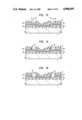
- FIG. 1 is a plan view of an LSI having a double-layer wiring structure in accordance with one embodiment of the present invention
- FIG. 2 is an enlarged sectional view taken along the line X--X of FIG. 1;
- FIGS. 3 to 5 are sectional views showing successive steps in the process for producing the LSI shown in FIGS. 1 and 2;
- FIG. 6 shows an ion beam machining apparatus and a laser CVD apparatus
- FIG. 7 is a plan view of an LSI, which shows another example of the structure for preventing shorting between wirings respectively located in the first- and second-level layers;
- FIG. 8 is an enlarged sectional view taken along the line Y--Y of FIG. 7;
- FIG. 9 is a plan view of an LSI in accordance with another embodiment of the present invention.
- FIG. 10 is an enlarged sectional view taken along the line X--X of FIG. 9;
- FIG. 11 is a plan view of an LSI in accordance with still another embodiment of the present invention.
- FIG. 12 is an enlarged sectional view taken along the line X--X of FIG. 11;
- FIGS. 13 to 15 are sectional views showing successive steps in the process for producing the LSI shown in FIGS. 11 and 12;
- FIGS. 16 and 17 show a method of interconnecting wirings in an IC in accordance with one embodiment of the present invention, FIG. 16 being a fragmentary plan view of the IC, and FIG. 17 being a sectional view taken along the line X--X of FIG. 16;
- FIGS. 18 and 19 show other embodiments, respectively, of the present invention.
- FIG. 20 shows experimental results of a machining process for forming a notch
- FIG. 21 is a sectional view taken along the line X--X of FIG. 20;
- FIG. 22 is a graph showing the experimental results shown in FIG. 20;
- FIG. 23 is a sectional view taken along the line Y--Y of FIG. 16;
- FIG. 24 is a sectional view taken along the line Z--Z of FIG. 23;
- FIGS. 25 to 27 show in combination an example of a machining method which enables elimination of a step from the machined surface
- FIG. 28 is a sectional view taken along the line Y--Y of FIG. 16, which shows experimental results of the example shown in FIGS. 25 to 27.
- FIG. 1 is a plan view of an LSI having a double-layer wiring structure in accordance with one embodiment of the present invention
- FIG. 2 is an enlarged sectional view taken along the line X--X of FIG. 1.
- the LSI in accordance with this embodiment has a semiconductor substrate (wafer) 1, for example, a silicon substrate, having a plurality of semiconductor elements such as transistors (not shown) fabricated thereon so as to form a semiconductor integrated circuit.
- An intermediate insulating film 2 for example, an SiO 2 film, is formed on the surface of the semiconductor substrate 1, and first-level wirings (i.e., lower-level wirings) 3a and 3b which are defined by, for example, an aluminum (Al) film, are provided on the intermediate insulating film 2.
- Another intermediate insulating film 4 which is defined by, for example, an SiO 2 film, is provided on the wirings 3a and 3b, and second-level wirings (i.e., upper-level wirings) 5a and 5b which are defined by, for example, an aluminum (Al) film, are provided on the intermediate insulating film 4.
- the wirings 5a and 5b define, for example, power supply wirings for supplying a power supply current, and are widely laid out over the surface of the intermediate insulating film 4.
- An insulating film 6 (not shown in FIG. 1) is further provided on the wirings 5a and 5b.
- Contact holes 7a and 7b are provided in such a manner as to extend through the insulating film 6, the wirings 5a, 5b (respectively) and the intermediate insulating film 4, and a connecting wiring 8 which interconnects the lower-level wirings 3a and 3b is provided in such a manner as to extend through these contact holes 7a and 7b.
- This connecting wiring 8 for example, a defect which is found after the completion of the LSI is repaired (or a logical design is changed).
- the contact holes 7a and 7b may be either vertical or tapered contact holes.
- the connecting wiring 8 is defined by a metal film such as a tungsten (W), molybdenum (Mo), cadmium (Cd) or aluminum (Al) film which is selectively formed by, for example, laser CVD.
- the surfaces of the second-level wirings 5a and 5b which are exposed through the respective contact holes 7a and 7b are provided with respective insulating films 9, for example, alumina (Al 2 O 3 ) films, which are formed by changing these surfaces into an insulator, thereby preventing contact between the connecting wiring 8 and the second-level wirings 5a, 5b. Accordingly, it is possible to form the connecting wiring 8 without any fear of the first-level wirings 3a, 3b electrically conducting, or shorting, to the second-level wirings 5a, 5b.
- the thickness of the insulating films 9 is selected so as to be adequate to obtain a necessary dielectric breakdown strength in accordance with the potential difference between the first-level wirings 3a, 3b and the second-level wirings 5a, 5b.
- the thickness of the films 9 may be selected so as to fall in the range from 1000 to 5000 ⁇ .
- a semiconductor integrated circuit is first formed on a silicon wafer 1 which serves as a starting material by carrying out diffusion of impurity ions, thermal oxidation of the silicon wafer 1, formation of thin films by CVD, formation of various patterns by the use of photolithographic techniques, etc. Then, an intermediate insulating film 2, first-level wirings 3a, 3b, an intermediate insulating film 4, second-level wirings 5a, 5b and an insulating film 6 are formed to complete an LSI. When it is necessary to find a possible defective part of the wirings and repair it, contact holes 7a and 7b are formed (see FIG.
- a lid 12 of a preliminary evacuation chamber 11 which defines a sample replacing chamber is first opened, and the above-described semiconductor wafer 1 is placed on a mount 14 which is installed on a stage 13. Then, the lid 12 is closed, and a valve 15 is opened to evacuate the preliminary evacuation chamber 11 by means of a vacuum pump 16.
- a gate valve 17 is opened, and the mount 14 is moved onto an XY stage 19 within a vacuum chamber which has been evacuated in advance by means of a vacuum pump 18.
- the reference numeral 20 denotes a valve which is normally opened.
- an ion beam 10 is drawn from a high-brightness ion source 22 such as a liquid metal ion source, e.g., gallium (Ga), which is provided within an ion beam lens tube 21 disposed at the upper side of the vacuum chamber by means of an extractor electrode 23 which is installed below the ion source 22, and the drawn ion beam 10 is then focused and deflected through electrostatic lenses 24, a blanking electrode 25, a deflector electrode 26, etc. so as to irradiate the semiconductor wafer 1.
- a high-brightness ion source 22 such as a liquid metal ion source, e.g., gallium (Ga)
- Ga gallium
- the semiconductor wafer 1 is transferred to, for example, an anodizing apparatus (not shown) to anodize the surfaces of the second-level wirings 5a and 5b which are exposed through the contact holes 7a and 7b formed as described above, thereby forming insulating films 9, e.g., alumina (Al 2 O 3 ) films, in self-alignment with the contact holes 7a and 7 b as shown in FIG. 4.
- anodizing process may be carried out using as a cathode platinum (Pt) and as an electrolyte a 5%-oxalic acid, phosphoric acid, chromic acid or sulfuric acid solution.
- insulating films 9 are also formed on the surfaces of the first-level wirings 3a and 3b within the contact holes 7a and 7b.
- the surfaces of the second-level wirings 5a and 5b which are exposed through the contact holes 7a and 7b are changed into an insulator and it is therefore possible to prevent shorting between the first-level wirings 3a, 3b and the second-level wirings 5a, 5b by a simple process without the need for a complicated process such as a photolithographic process.
- the above-described alumina film may also be formed by, for example, O 2 plasma oxidation, in addition to anodizing.
- O 2 plasma oxidation technique is described, for example, in "Vacuum", Vol. 27, No. 12 (1984), p.901.
- materials other than aluminum (Al) for example, refractory metals such as tungsten (W), molybdenum (Mo) or the like, are employed as a wiring material, oxides of these metals can be formed, for example, by subjecting the metals to a low-temperature heat treatment while irradiating them with ozone, and thus defining the insulating films 9.
- a wiring material e.g., aluminum
- this problem can be eliminated by completely changing the aluminum deposited on the inner peripheral surfaces of the contact holes 7a and 7b into alumina by, for example, the above-described anodizing.
- the insulating films 9 which are formed on the surfaces of the first-level wirings 3a and 3b in the contact holes 7a and 7b as the result of the above-described anodizing are selectively removed by, for example, irradiation with a laser beam, thereby partially exposing the surfaces of the first-level wirings 3a and 3b, as shown in FIG. 5.
- the semiconductor wafer 1 is replaced on the mount 14 provided on the XY stage 13 shown in FIG. 6 and the mount 14 is moved onto an XY stage 30 within a vacuum chamber 29 of the laser CVD apparatus.
- the semiconductor wafer 1 is then moved by the operation of the XY stage 30 to a position where the wafer 1 is to be irradiated with a laser beam 32 oscillated from a laser oscillator 31, for example, an argon laser, thereby positioning the defective part of the wirings which is to be repaired.
- a laser beam 32 oscillated from a laser oscillator 31, for example, an argon laser for example, an argon laser
- the laser beam 32 is passed through a shutter 33, reflected by a dichroic mirror 34 and focused by an objective lens 35 so as to irradiate said part of the wirings through a window 36 which is provided in the wall of the vacuum chamber 29.
- a valve 42 is opened to introduce a reaction gas consisting of an organic metal compound, e.g., Mo(CO) 6 or W(CO) 6 , into the vacuum chamber 29 from a gas cylinder 43 which is connected to the chamber 29.
- a valve 44 is opened to introduce an inert gas into the vacuum chamber 29 from a gas cylinder 45.
- the laser beam 29 is selectively applied to the defective part of the wirings, thereby decomposing the reaction gas and selectively depositing a metal on the part irradiated with the laser beam 32.
- the connecting wiring 8 which interconnects the wirings 3a and 3b in the first-level layer through the contact holes 7a and 7b is formed as shown in FIGS. 1 and 2.
- the defective part is repaired when the LSI is in the form of the semiconductor wafer 1, it is, of course, possible to repair the defective part after the semiconductor wafer 1 has been divided into individual semiconductor chips.
- repair of a defective part of the wirings or change of the logical design is effected after the completion of the LSI, it is also possible to apply the present invention to formation of wirings for realizing a desired logic in, for example, a master slice or a gate array.
- the present invention may be applied to formation of a connecting wiring which interconnects wiring in the same layer or different layers in the course of the process for producing, for example, an LSI having a multilayer wiring structure.
- the present invention may also be applied to, for example, a printed board having a multilayer wiring structure.
- FIG. 9 is a plan view of an LSI having a double-layer wiring structure in accordance with another embodiment of the present invention
- FIG. 10 is an enlarged sectional view taken along the line X--X of FIG. 9.
- the LSI in accordance with this embodiment has a semiconductor substrate (wafer) 1, for example, a silicon substrate, having a plurality of semiconductor elements such as transistors (not shown) fabricated thereon so as to form a semiconductor integrated circuit.
- An intermediate insulating film 2 for example, an SiO 2 film, is formed on the surface of the semiconductor substrate 1, and first-level wirings (i.e., lower-level wirings) 3a and 3b which are defined by, for example, an aluminum (Al) film, are provided on the intermediate insulating film 2.
- Another intermediate insulating film 4 which is defined by, for example, an SiO 2 film, is provided on the wirings 3a and 3b, and second-level wirings (i.e., upper-level wirings) 5a and 5b which are defined by, for example, an aluminum (Al) film, are provided on the intermediate insulating film 4.
- the wirings 5a and 5b define, for example, power supply wirings for supplying a power supply current, and are widely laid out over the surface of the intermediate insulating film 4.
- An insulating film 6 (not shown in FIG. 9) is further provided on the wirings 5a and 5b.
- Contact holes 7a and 7b are provided in such a manner as to extend through the insulating film 6, the wirings 5a, 5b (respectively) and the intermediate insulating film 4, and a connecting wiring 8 which interconnects the lower-level wirings 3a and 3b is provided in such a manner as to extend through these contact holes 7a and 7b.
- this connecting wiring 8 for example, a defect which is found after the completion of the LSI is repaired (or a logical design is changed).
- the contact holes 7a and 7b may be either vertical or tapered contact holes.
- the connecting wiring 8 consists of a buffer film 8A such as a chromium (Cr) film and a metal film 8B such as a tungsten film.
- the metal film 8B is defined by a single-layer film consisting of tungsten (W), molybdenum (Mo), cadmium (Cd) or aluminum (Al), or a multilayer film consisting of these metals, the single- or multi-layer film being selectively formed by means, for example, of laser CVD.
- the buffer film 8A which is the other constituent element of the connecting wiring 8 is formed specifically from a metal such as chromium (Cr), molybdenum (Mo), tungsten (W) or nickel (Ni), or a semiconductor, such as Si, Ge, GaAs or polysilicon, which contains an active impurity, or a silicide which is an alloy of a metal and silicon.
- a metal such as chromium (Cr), molybdenum (Mo), tungsten (W) or nickel (Ni)
- a semiconductor such as Si, Ge, GaAs or polysilicon, which contains an active impurity, or a silicide which is an alloy of a metal and silicon.
- the buffer film 8A Since the buffer film 8A has a high rate of absorption of a laser beam which causes the CVD phenomenon, it is possible to deposit a wiring material without the need to increase the laser output, and it is therefore possible to effect CVD with excellent controllability. In other words, it is possible to provide a wiring even if scanning with the laser beam is effected at high speed.
- the buffer film 8A since the presence of the buffer film 8A makes it possible to lessen the effects of the material and structure of the ground on which a wiring material is to be provided, it is easy to maintain the width and thickness of the wiring deposited on the buffer film 8A at constant levels. At the same time, the buffer film 8A absorbs the greater part of the energy of the laser beam and reflects part of the laser beam, and it is therefore possible to reduce the thermal effect of the wiring on the ground. It has been experimentally confirmed that, as the buffer film 8A, chromium (Cr) film is particularly preferable and practical.
- the surfaces of the second-level wirings 5a and 5b which are exposed through the respective contact holes 7a and 7b are provided with respective insulating films 9, for example, alumina (Al 2 O 3 ) films, which are formed by changing the surfaces into an insulator, thereby preventing contact between the connecting wiring 8 and the second-level wirings 5a, 5b. Accordingly, it is possible to form the connecting wiring 8 without any fear of the first-level wirings 3a, 3b electrically conducting, or shorting, to the second-level wirings 5a, 5b.
- the thickness of the insulating films 9 is selected so as to be adequate to obtain a necessary dielectric breakdown strength in accordance with the potential difference between the first-level wirings 3a, 3b and the second-level wirings 5a, 5b.
- the thickness of the films 9 may be selected so as to fall in the range from 1000 to 5000 ⁇ .
- the LSI in accordance with this embodiment can be produced by appropriating the process for producing a buffer film disclosed in Japanese Patent Application No. 245215/1986 to the process for producing an LSI in accordance with the foregoing first embodiment.
- the defective part is repaired when the LSI is in the form of the semiconductor wafer 1, it is, of course, possible to repair the defective part after the semiconductor wafer 1 has been divided into individual semiconductor chips.
- repair of a defective part of the wirings or change of the logical design is effected after the completion of the LSI, it is also possible to apply the present invention to formation of wirings for realizing a desired logic in, for example, a master slice or a gate array.
- the present invention may be applied to formation of a connecting wiring which interconnects wirings in the same layer or different layers in the course of the process for producing, for example, an LSI having a multilayer wiring structure.
- the present invention may also be applied to, for example, a printed board having a multilayer wiring structure.
- FIG. 11 is a plan view of an LSI having a double-layer wiring structure in accordance with still another embodiment of the present invention
- FIG. 12 is an enlarged sectional view taken along the line X--X of FIG. 11.
- the LSI in accordance with this embodiment has a semiconductor substrate (wafer) 1, for example, a silicon substrate, having a plurality of semiconductor elements such as transistors (not shown) fabricated thereon so as to form a semiconductor integrated circuit.
- An intermediate insulating film 2 for example, an SiO 2 film, is formed on the surface of the semiconductor substrate 1, and first-level wirings (i.e., lower-level wirings) 3a and 3b which re defined by, for example, an aluminum (Al) film are provided on the intermediate insulating film 2.
- Another intermediate insulating film 4 which is defined by, for example, an SiO 2 film is provided on the wirings 3a and 3b, and second-level wirings (i.e., upper-level wirings) 5a and 5b which are defined by, for example, an aluminum (Al) film, are provided on the intermediate insulating film 4.
- the wirings 5a and 5b define, for example, power supply wirings for supplying a power supply current, and are widely laid out over the surface of the intermediate insulating film 4.
- An insulating film 6 (not shown in FIG. 11) is further provided on the wirings 5a and 5b.
- Contact holes 7a and 7b are provided in such a manner as to extend through the insulating film 6, the wirings 5a, 5b (respectively) and the intermediate insulating film 4, and a connecting wiring 8 which interconnects the lower-level wirings 3a and 3b is provided in such a manner as to extend through these contact holes 7a and 7b.
- This connecting wiring 8 for example, a defect which is found after the completion of the LSI is repaired (or a logical design is changed).
- the contact holes 7a and 7b may be either vertical or tapered contact holes.
- the connecting wiring 8 is defined by a metal film such as a tungsten (W), molybdenum (Mo), cadmium (Cd) or aluminum (Al) film which is selectively formed by, for example, laser CVD.
- the second-level wirings 5a and 5b which are exposed through the respective contact holes 7a and 7b are provided with respective bores 5c and 5d which have a larger diameter than that of the contact holes 7a and 7b, as will be clear from FIG. 12, thereby preventing contact between the connecting wiring 8 and the second-level wirings 5a, 5b. Accordingly, it is possible to form the connecting wiring 8 without any fear of the first-level wirings 3a, 3b electrically conducting, or shorting, to the second-level wirings 5a, 5b.
- a semiconductor integrated circuit is first formed on a silicon wafer 1 which serves as a starting material by carrying out diffusion of impurity ions, thermal oxidation of the silicon wafer 1, formation of thin films by CVD, formation of various patterns by the use of photolithographic techniques, etc. Then, an intermediate insulating film 2, first-level wirings 3a, 3b, an intermediate insulating film 4, second-level wirings 5a, 5b and an insulating film 6 are formed to complete an LSI.
- contact holes 7a and 7b are formed by irradiating predetermined portions of the surface of the insulating film 6 with a focused ion beam 10 (see FIG. 13) having a high degree of machining accuracy by using, for example, an ion beam machining apparatus such as that shown in FIG. 6 which is proposed in the aforementioned Japanese Patent Application No. 70979/1986.
- the second-level wirings 5a and 5b e.g., aluminum (Al) film, the surfaces of which are exposed through the contact holes 7a and 7b are etched by wet etching using the insulating film 6 as an etching mask to thereby form bores 5c and 5d in the second-level wirings 5a and 5b, the bores 5c and 5d having a larger diameter than that of the contact holes 7a and 7b.
- Al aluminum
- the diameter A of the bores 5c and 5d is set at a value which is, for example, about 4 ⁇ m larger than the diameter B of the contact holes 7a and 7b so that the edge of each of the bores 5c and 5d provided in the second-level wirings 5a and 5b is located at a position about 2 ⁇ m recessed from the edge of the corresponding one of the contact holes 7a and 7b.
- the above-described configuration of the bores 5c and 5d prevents the connecting wiring 8 (described later) from being electrically connected, or shorted, to the second-level wirings 5a, 5b.
- the dimensions of the bores 5c and 5d provided in the second-level wirings 5a and 5b may be so selected that the connecting wiring 8 which is connected to the first-level wirings 3a and 3b through the contact holes 7a and 7b is prevented from electrically connected to the second-level wirings 5a and 5b by the presence of the bores 5c and 5d.
- the second-level wirings 5a and 5b are formed using, for example, aluminum or a material containing aluminum as its principal component, e.g., aluminum containing about 0.5 to 1.0% of silicon (Si).
- a wet etching solution which may be employed to etch such a material containing aluminum as its principal component, it is preferable to use a mixed solution obtained by mixing together phosphoric acid, glacial acetic acid, nitric acid and water in the volume ratios 76:15:3:5.
- This etching solution is capable of etching not only aluminum but also alumina (Al 2 O 3 ) which is an oxide of aluminum.
- the regions of the intermediate insulating film 4 the surfaces of which are exposed through the contact holes 7a and 7b are irradiated with a focused ion beam of high degree of machining accuracy by the use of an ion beam machining apparatus to thereby form bores 4a and 4b.
- bores 4a and 4b which have substantially the same diameter as that of the contact holes 7a and 7b are formed thereunder.
- a metal film such as tungsten (W) or molybdenum (Mo) is formed in a predetermined pattern by scanning it with a laser beam by laser CVD which is an optically pumped CVD method, as shown in FIGS. 11 and 12.
- connection wiring 8 and the second-level wirings 5a, 5b are electrically isolated from each other by the air gap regions 5e and 5f.
- electrical isolation of the connecting wiring 8 from the second-level wirings 5a, 5b is effected by the air gap regions 5e and 5f which are formed by partially removing the second-level wirings 5a and 5b by wet etching.
- this embodiment which employs wet etching, has the merit that it is possible to provide an electrical isolation means in a simple operation and within a short period of time in comparison with the method described in the first embodiment. Since the isolation method by anodizing which has been described in the first embodiment is carried out by dipping the sample in an electrolytic bath containing an electrolyte, the electrolyte and various contaminants adhere to the sample, and a complicated process is needed to completely clean the attached electrolyte and contaminants.
- LSI There is one type of LSI for computers which has a large number of bump electrodes made of a solder material as external lead terminals and which is mounted on a circuit board through the bump electrodes by CCD (Controlled Collapse Bonding) method, and some of these LSIs have several hundreds of bump electrodes on the plane of an LSI chip of, for example, 10 mm ⁇ 10 mm.
- CCD Controlled Collapse Bonding
- the bump electrodes may also be undesirably anodized, which gives rise to problems such as lowering in the electrical characteristics and occurrence of a failure.
- the isolation method by wet etching described in this embodiment enables the etching solution attached to the sample to be completely cleaned (removed) in a simple operation and within a short period of time and this isolation method is free from various problems which are experienced with the anodizing process. Therefore, it should be borne in mind that the isolation method in accordance with this embodiment is more practical than the anodizing method and is a superior method which does not lead to deterioration in electrical characteristics nor lowering in reliability of the sample.
- connecting wiring 8 in this embodiment it is possible to employ the composite film of the buffer film 8A and the metal film 8B which has been described in the second embodiment.
- the defective part is repaired when the LSI is in the form of the semiconductor wafer 1, it is, of course, possible to repair the defective part after the semiconductor wafer 1 has been divided into individual semiconductor chips.
- repair of a defective part of the wirings or change of the logical design is effected after the completion of the LSI, it is also possible to apply the present invention to formation of wirings for realizing a desired logic in, for example, a master slice or a gate array.
- the present invention may be applied to formation of a connecting wiring which interconnects wirings in the same layer or different layers in the course of the process for producing, for example, an LSI having a multilayer wiring structure.
- the present invention may also be applied to, for example, a printed board having a multilayer wiring structure.
- a hole is bored by means of a focused ion beam in that portion of an insulating film which is located above that portion of a wiring which is desired to be connected to another portion, and said portion of the wiring is irradiated with a focused laser or ion beam in a metal compound gas to deposit a metal in the above-described hole, thereby forming a wiring.
- the hole is machined so that the upper portion of the hole is widened, and the metal is buried in the hole in such a manner that a particularly large amount of metal is deposited in the upper portion of the hole, thereby enabling the deposited metal to be satisfactorily connected to the wiring at the lower side of the hole.
- the positions of a plurality of wirings which are to be interconnected are detected by employing a scanning ion microscope using a secondary electron or ion signal obtained from the sample, thereby positioning the sample and determining portions to be irradiated with an ion beam. Thereafter, said portions of the sample are irradiated with the ion beam to remove those portions of the insulating film which are located above said portions of the wirings. Since in this case a focused ion beam is employed instead of a laser beam, it is possible to effect machining on the order of 0.5 ⁇ m or less with the focused ion beam.
- the ion beam enables any kind of material to be uniformly machined, it is possible to machine a stack of insulating films such as SiO 2 and Si 3 N 4 successively from the upper side thereof and thereby bore a hole therein to expose the surface of the wiring in the lower layer.
- a metal compound gas is introduced into the vacuum chamber through a nozzle or a pipe, and the sample table is moved relative to the vacuum chamber so that portion of the sample where a connecting wiring is to be formed is irradiated with a focused ion or laser beam.
- a metal wiring is formed by ion beam induced CVD process or laser DVD process.
- debugging of ICs includes finding and correcting an error in connection of the wirings in ICs and making a diagnosis of ICs.
- the feature of this embodiment also resides in a method of notching that portion of the upper-level wiring which is in contact with the buried metal in order to prevent the metal which is buried to provide connection with the lower-level wiring from electrically conducting to the upper-level wiring.
- FIGS. 16 and 17 show in combination a method of forming a connecting wiring on an IC in accordance with one embodiment of the present invention.
- an insulating film (e.g., a SiO 2 film) 101 is provided on a substrate (e.g., a Si substrate), and wirings (e.g., Al wirings) 102a, 102b and 102c are formed on the insulating film 101 with an insulating film 101 interposed between each pair of adjacent wirings. Further, a protective film (e.g., a SiO 2 or Si 3 N 4 film) 101 is formed on the uppermost wiring 102c.
- a protective film e.g., a SiO 2 or Si 3 N 4 film
- holes 103a and 103b are bored in the insulating films 101 above the wiring 102a by means of a focused ion beam to thereby expose a part of the wiring 102a. Thereafter, a metal wiring 104 is buried in the holes 103a and 103b by laser induced CVD or other similar means and the metal wiring 104 is then formed so as to extend to a desired node or point of connection.
- the metal wiring 104 Prior to the formation of the metal wiring 104, it is also possible to form a structure in which a buffer film is provided under the metal wiring 104 as described in the second embodiment.
- the connecting wiring Since the IC has a multilayer wiring structure, if a connecting wiring is to be led from the first-level (lowermost) wiring 102a, the connecting wiring must be prevented from coming into contact with the upper-level wirings. In the arrangement shown in FIG. 16, a hole is bored at a position which is spaced apart from the second-level wiring 102b.
- the third-level (uppermost) wiring 102c is usually used as a power supply wiring and therefore has a relatively wide width W as shown in FIG. 16. Accordingly, it is difficult to bore a hole for burying a connecting wiring at a position which is off the third-level wiring 102c.
- a notch 105 (having a width W) shown in FIG. 16 is cut outside the hole 103b so that the depth Z of the notch 105 is slightly greater than the depth of the third-level wiring 102c, thereby electrically isolating that portion of the third-level wiring 102c which is in contact with the metal wiring 104 from the other portion of the wiring 102c.
- a metal wiring is formed by laser CVD or other similar means so as to extend through the area defined between the two ends of the notch 105 having a U-shaped planar configuration.
- the wiring 102c may be notched diagonally. By doing so, it is advantageously possible to simplify the scanning with the ion beam.
- the notch 105 may be circular as shown in FIG. 19. In this case, it is possible to readily carry out scanning with the ion beam by superposing sine waves in the X- and Y-directions one upon the other.
- the second-level wiring 102b is present below the notch 105 as shown in FIG. 16, care must be taken of the following point.
- the second-level wirings are often arranged at a pitch of, for example, 5 to 10 ⁇ m, because the integration density of ICs is increasing these days. Therefore, if the holes 103a and 103b are positioned so as to be spaced apart from the second-level wiring 102b, there is a good possibility that the notch 105 will overlap the wiring 102b. In such a case, it is important to appropriately control the depth of the notch 105.
- FIG. 23 is a sectional view taken along the line Y--Y of FIG. 16. Since the step of the third-level wiring 102c causes the protective film 101 to have a step 106, the configuration of the step 106 is reflected on the bottom surface of the notch 105 as will be clear from the above-described experimental results, so that the second-level wiring 102b is partially etched. As a result, as shown in FIG. 24 which is a sectional view taken along the line Z--Z of FIG.
- the cross-sectional area of the second-level wiring 102b is reduced, which results in the reliability of the device being deteriorated, or when the second-level wiring 102b is subjected to sputter etching, the wiring material adheres to the side walls of the notch 105 as shown by the reference numeral 107 and the wiring material 107 attached to the side walls may short the second- and third-level wirings.
- the edge portion 108 of the step 106 is detected with a secondary particle image as shown in FIG. 20, and scanning with a focused ion beam 109 is started from the edge portion 108 as shown in FIG. 25.
- the depth Z(t) of machining shown in FIG. 26 is proportional to the machining time t in the case where the ion current is adequately stable (within ⁇ 5% in the case of ordinary apparatus)
- the depth Z(t) is determined as a function of the time t.
- the angle ⁇ of inclination of the step 6 is constant for the devices produced by the same film forming process and therefore can be known in advance. Accordingly, it is possible to start machining from the edge portion 108 shown in FIG.
- the metal wiring 104 is formed so as to extend between desired points of connection by laser or ion beam induced CVD, thereby interconnecting the lower-level wiring 102b and another wiring.
- the present invention makes it possible to interconnect as desired wirings which are located at different positions in an IC which has a high integration density and a multilayer wiring structure, so that it is possible to readily carry out a defect analysis in any stage of fabrication of LSIs, i.e., designing, trial production and mass production of LSIs.
- a defect analysis in any stage of fabrication of LSIs, i.e., designing, trial production and mass production of LSIs.
Abstract
Description
Claims (31)
Applications Claiming Priority (4)
| Application Number | Priority Date | Filing Date | Title |
|---|---|---|---|
| JP61-298731 | 1986-12-17 | ||
| JP61298731A JPH081928B2 (en) | 1986-12-17 | 1986-12-17 | Method for forming connection wiring structure of multilayer wiring |
| JP61-303719 | 1986-12-22 | ||
| JP61303719A JPH084089B2 (en) | 1986-12-22 | 1986-12-22 | IC element and wiring connection method in IC element |
Publications (1)
| Publication Number | Publication Date |
|---|---|
| US4900695A true US4900695A (en) | 1990-02-13 |
Family
ID=26561636
Family Applications (1)
| Application Number | Title | Priority Date | Filing Date |
|---|---|---|---|
| US07/134,460 Expired - Lifetime US4900695A (en) | 1986-12-17 | 1987-12-17 | Semiconductor integrated circuit device and process for producing the same |
Country Status (1)
| Country | Link |
|---|---|
| US (1) | US4900695A (en) |
Cited By (85)
| Publication number | Priority date | Publication date | Assignee | Title |
|---|---|---|---|---|
| US5028780A (en) * | 1988-12-01 | 1991-07-02 | Seiko Instruments, Inc. | Preparation and observation method of micro-section |
| US5043297A (en) * | 1989-09-05 | 1991-08-27 | Hitachi, Ltd. | Wiring method of on-chip modification for an LSI |
| US5049525A (en) * | 1990-06-29 | 1991-09-17 | Texas Instruments Incorporated | Iterative self-aligned contact metallization process |
| US5086015A (en) * | 1988-08-24 | 1992-02-04 | Hitachi, Ltd. | Method of etching a semiconductor device by an ion beam |
| DE4128568A1 (en) * | 1990-08-28 | 1992-03-05 | Hitachi Ltd | MULTILAYER WIRING METHOD FOR MODIFYING THE CHIP FOR A HIGHLY INTEGRATED SEMICONDUCTOR CIRCUIT (LSI) |
| US5106780A (en) * | 1988-08-05 | 1992-04-21 | Kabushiki Kaisha Toshiba | Semiconductor device and method of manufacturing the same |
| US5122859A (en) * | 1990-06-29 | 1992-06-16 | Texas Instruments Incorporated | Iterative self-aligned contact metallization process |
| US5169802A (en) * | 1991-06-17 | 1992-12-08 | Hewlett-Packard Company | Internal bridging contact |
| US5171709A (en) * | 1988-07-25 | 1992-12-15 | International Business Machines Corporation | Laser methods for circuit repair on integrated circuits and substrates |
| US5182230A (en) * | 1988-07-25 | 1993-01-26 | International Business Machines Corporation | Laser methods for circuit repair on integrated circuits and substrates |
| US5185291A (en) * | 1989-06-30 | 1993-02-09 | At&T Bell Laboratories | Method of making severable conductive path in an integrated-circuit device |
| US5204286A (en) * | 1991-10-15 | 1993-04-20 | Micron Technology, Inc. | Method of making self-aligned contacts and vertical interconnects to integrated circuits |
| US5252517A (en) * | 1992-12-10 | 1993-10-12 | Micron Semiconductor, Inc. | Method of conductor isolation from a conductive contact plug |
| US5306667A (en) * | 1991-12-17 | 1994-04-26 | Intel Corporation | Process for forming a novel buried interconnect structure for semiconductor devices |
| US5330935A (en) * | 1990-10-24 | 1994-07-19 | International Business Machines Corporation | Low temperature plasma oxidation process |
| US5358903A (en) * | 1992-06-16 | 1994-10-25 | Hyundai Electronics Industries Co. Ltd. | Contact of a semiconductor device and its manufacturing process |
| US5381004A (en) * | 1993-08-31 | 1995-01-10 | Applied Materials, Inc. | Particle analysis of notched wafers |
| US5393701A (en) * | 1993-04-08 | 1995-02-28 | United Microelectronics Corporation | Layout design to eliminate process antenna effect |
| US5408130A (en) * | 1992-08-31 | 1995-04-18 | Motorola, Inc. | Interconnection structure for conductive layers |
| US5442238A (en) * | 1991-04-05 | 1995-08-15 | Mitsubishi Denki Kabushiki Kaisha | Interconnection structure of a semiconductor device |
| US5474945A (en) * | 1991-03-06 | 1995-12-12 | Semiconductor Energy Laboratory Co., Ltd. | Method for forming semiconductor device comprising metal oxide |
| US5547906A (en) * | 1992-09-14 | 1996-08-20 | Badehi; Pierre | Methods for producing integrated circuit devices |
| US5568288A (en) * | 1991-03-26 | 1996-10-22 | Semiconductor Energy Laboratory Co., Ltd. | Method for forming thin film transistors with anodic oxide on sides of gate line |
| US5639344A (en) * | 1994-05-11 | 1997-06-17 | Semiconductor Energy Laboratory Co., Ltd. | Etching material and etching process |
| US5716759A (en) * | 1993-09-02 | 1998-02-10 | Shellcase Ltd. | Method and apparatus for producing integrated circuit devices |
| US5726098A (en) * | 1994-09-22 | 1998-03-10 | Nec Corporation | Method of manufacturing semiconductor device having multilevel interconnection |
| US5753375A (en) * | 1995-01-05 | 1998-05-19 | Santa Barbara Research Center | Microelectronic device having dark mirror coating with vias therethrough |
| US5821549A (en) * | 1997-03-03 | 1998-10-13 | Schlumberger Technologies, Inc. | Through-the-substrate investigation of flip-chip IC's |
| US5824598A (en) * | 1986-03-31 | 1998-10-20 | Hitachi, Ltd. | IC wiring connecting method using focused energy beams |
| US5863833A (en) * | 1994-12-14 | 1999-01-26 | Samsung Electronics Co., Ltd. | Method for forming side contact in a semiconductor device |
| US5888852A (en) * | 1996-03-01 | 1999-03-30 | Matsushita Electric Industrial Co., Ltd. | Method for forming semiconductor microstructure, semiconductor device fabricated using this method, method for fabricating resonance tunneling device, and resonance tunnel device fabricated by this method |
| US5912668A (en) * | 1997-05-30 | 1999-06-15 | Sony Corporation | Controlling a screen display of a group of images represented by a graphical object |
| US5913112A (en) * | 1991-03-06 | 1999-06-15 | Semiconductor Energy Laboratory Co., Ltd. | Method of manufacturing an insulated gate field effect semiconductor device having an offset region and/or lightly doped region |
| US5933704A (en) * | 1997-06-02 | 1999-08-03 | Taiwan Semiconductor Manufacturing Company, Ltd. | Method to reveal the architecture of multilayer interconnectors in integrated circuits |
| US5956105A (en) * | 1991-06-14 | 1999-09-21 | Semiconductor Energy Laboratory Co., Ltd. | Electro-optical device and method of driving the same |
| USRE36314E (en) * | 1991-03-06 | 1999-09-28 | Semiconductor Energy Laboratory Co., Ltd. | Insulated gate field effect semiconductor devices having a LDD region and an anodic oxide film of a gate electrode |
| US5990555A (en) * | 1996-05-14 | 1999-11-23 | Fujitsu Limited | Electronic circuit device with multi-layer wiring |
| US6037246A (en) * | 1996-09-17 | 2000-03-14 | Motorola Inc. | Method of making a contact structure |
| US6040235A (en) * | 1994-01-17 | 2000-03-21 | Shellcase Ltd. | Methods and apparatus for producing integrated circuit devices |
| USRE36663E (en) * | 1987-12-28 | 2000-04-18 | Texas Instruments Incorporated | Planarized selective tungsten metallization system |
| US6117707A (en) * | 1994-07-13 | 2000-09-12 | Shellcase Ltd. | Methods of producing integrated circuit devices |
| DE4435585C2 (en) * | 1994-10-05 | 2001-02-01 | Micronas Gmbh | Connection structure for double layers, in particular for use in integrated semiconductor circuits |
| US6274492B1 (en) | 1996-05-31 | 2001-08-14 | Technische Universitaet Dresden | Process and device for production of metallic coatings on semiconductor structures |
| US6295121B1 (en) * | 1996-01-05 | 2001-09-25 | Canon Kabushiki Kaisha | Exposure apparatus |
| US20020053734A1 (en) * | 1993-11-16 | 2002-05-09 | Formfactor, Inc. | Probe card assembly and kit, and methods of making same |
| US6444484B1 (en) * | 1997-03-06 | 2002-09-03 | Lg Electronics, Inc. | Wiring structure of thin film transistor array and method of manufacturing the same |
| US20020197851A1 (en) * | 2000-12-29 | 2002-12-26 | Ilan Gavish | Focused ion beam deposition |
| US20030003611A1 (en) * | 2001-06-29 | 2003-01-02 | Kla-Tencor Corporation | Apparatus and methods for monitoring self-aligned contact arrays |
| US6580072B1 (en) | 2000-05-03 | 2003-06-17 | Xilinx, Inc. | Method for performing failure analysis on copper metallization |
| US20030155927A1 (en) * | 1999-12-14 | 2003-08-21 | Kla Tencor Technologies Corporation | Multiple directional scans of test structures on srmiconductor integrated circuits |
| US6624450B1 (en) | 1992-03-27 | 2003-09-23 | Semiconductor Energy Laboratory Co., Ltd. | Semiconductor device and method for forming the same |
| US20030199179A1 (en) * | 1993-11-16 | 2003-10-23 | Formfactor, Inc. | Contact tip structure for microelectronic interconnection elements and method of making same |
| US6638580B2 (en) * | 2000-12-29 | 2003-10-28 | Intel Corporation | Apparatus and a method for forming an alloy layer over a substrate using an ion beam |
| US6692995B2 (en) * | 2002-04-05 | 2004-02-17 | Intel Corporation | Physically deposited layer to electrically connect circuit edit connection targets |
| US6778231B1 (en) | 1991-06-14 | 2004-08-17 | Semiconductor Energy Laboratory Co., Ltd. | Electro-optical display device |
| US20040217305A1 (en) * | 2003-02-18 | 2004-11-04 | Stmicroelectronics S.A. | Method of repairing an integrated electronic circuit, comprising the formation of an electrical isolation |
| US6815762B2 (en) * | 1997-05-30 | 2004-11-09 | Hitachi, Ltd. | Semiconductor integrated circuit device and process for manufacturing the same including spacers on bit lines |
| US6861666B1 (en) | 2001-10-17 | 2005-03-01 | Kla-Tencor Technologies Corporation | Apparatus and methods for determining and localization of failures in test structures using voltage contrast |
| US6863733B1 (en) * | 1999-07-15 | 2005-03-08 | Nec Corporation | Apparatus for fabricating thin-film semiconductor device |
| US6893978B1 (en) * | 2002-12-03 | 2005-05-17 | Silicon Magnetic Systems | Method for oxidizing a metal layer |
| US6906129B2 (en) | 2003-09-05 | 2005-06-14 | Shin-Etsu Chemical Co., Ltd. | Polymer scale preventive agent |
| US20050161822A1 (en) * | 2004-01-23 | 2005-07-28 | Nec Electronics Corporation | Integrated circuit device |
| US20050191767A1 (en) * | 2004-03-01 | 2005-09-01 | Edwards Henry L. | Focused ion beam circuit repair using a hardmask and wet chemistry |
| US6975296B1 (en) | 1991-06-14 | 2005-12-13 | Semiconductor Energy Laboratory Co., Ltd. | Electro-optical device and method of driving the same |
| US20060051508A1 (en) * | 2000-12-28 | 2006-03-09 | Ilan Gavish | Focused ion beam deposition |
| US20060109459A1 (en) * | 2004-10-19 | 2006-05-25 | Matthias Kramer | Microscope with laser light source and protective device for preventing eye damage |
| US20060178001A1 (en) * | 2005-02-05 | 2006-08-10 | Lin Steven Gs | Method for fabricating interconnection in an insulating layer on a wafer and structure thereof |
| US20060237856A1 (en) * | 1993-11-16 | 2006-10-26 | Formfactor, Inc. | Microelectronic Contact Structure And Method Of Making Same |
| US20070111342A1 (en) * | 2000-04-18 | 2007-05-17 | Kla Tencor | Chemical mechanical polishing test structures and methods for inspecting the same |
| US20070152174A1 (en) * | 2004-09-10 | 2007-07-05 | Hitachi High-Technologies Corporation | Focused ion beam apparatus and aperture |
| US20080230910A1 (en) * | 2007-03-24 | 2008-09-25 | Minka Gospodinova-Daltcheva | Integrated circuit and method for producing the same |
| US7470631B1 (en) * | 1998-03-05 | 2008-12-30 | Micron Technology, Inc. | Methods for fabricating residue-free contact openings |
| US20100093229A1 (en) * | 1996-02-21 | 2010-04-15 | Formfactor, Inc. | Microelectronic contact structure and method of making same |
| US20100260410A1 (en) * | 2009-04-08 | 2010-10-14 | United States of America as represented by the Administrator of the National Aeronautics and | Closed-Loop Process Control for Electron Beam Freeform Fabrication and Deposition Processes |
| US20100270274A1 (en) * | 2009-04-28 | 2010-10-28 | Usa As Represented By The Administrator Of The National Aeronautics And Space Administration | Use of Beam Deflection to Control an Electron Beam Wire Deposition Process |
| US20110223966A1 (en) * | 2003-02-24 | 2011-09-15 | Semiconductor Energy Laboratory Co., Ltd. | Thin film integrated circuit device, ic label, container comprising the thin film integrated circuit, manufacturing method of the thin film integrated circuit device, manufacturing method of the container, and management method of product having the container |
| US9196591B2 (en) * | 2014-02-17 | 2015-11-24 | International Business Machines Corporation | Chip with shelf life |
| US9245846B2 (en) | 2014-05-06 | 2016-01-26 | International Business Machines Corporation | Chip with programmable shelf life |
| US9764415B2 (en) | 2013-03-15 | 2017-09-19 | The United States Of America As Represented By The Administrator Of Nasa | Height control and deposition measurement for the electron beam free form fabrication (EBF3) process |
| US10101601B2 (en) * | 2016-05-11 | 2018-10-16 | Shenzhen China Star Optoelectronics Technology Co., Ltd. | Broken line repair method of TFT substrate |
| US20190035676A1 (en) * | 2017-07-31 | 2019-01-31 | Taiwan Semiconductor Manufacturing Co., Ltd. | Method for manufacturing semiconductor device, method for packaging semiconductor chip, method for manufacturing shallow trench isolation (sti) |
| US10211349B2 (en) * | 2009-12-01 | 2019-02-19 | Sunpower Corporation | Solar cell contact formation using laser ablation |
| US20190076958A1 (en) * | 2017-09-14 | 2019-03-14 | Fanuc Corporation | Laser machining device for correcting processing conditions before laser machining based on contamination level of optical system |
| US10672648B2 (en) * | 2017-03-31 | 2020-06-02 | United Microelectronics Corp. | Method of forming semiconductor memory device |
| CN112117175A (en) * | 2019-06-21 | 2020-12-22 | Fei 公司 | Perimeter trench formation and demarcated etch-away layer |
Citations (4)
| Publication number | Priority date | Publication date | Assignee | Title |
|---|---|---|---|---|
| US4630357A (en) * | 1985-08-02 | 1986-12-23 | Ncr Corporation | Method for forming improved contacts between interconnect layers of an integrated circuit |
| JPS62751A (en) * | 1985-06-25 | 1987-01-06 | Matsushita Electric Ind Co Ltd | Control device of air conditioner |
| US4675979A (en) * | 1984-12-19 | 1987-06-30 | Eaton Corporation | Method for making horizontally layered momom tunnel device |
| US4675980A (en) * | 1984-12-19 | 1987-06-30 | Eaton Corporation | Method for making vertically layered MOMOM tunnel device |
-
1987
- 1987-12-17 US US07/134,460 patent/US4900695A/en not_active Expired - Lifetime
Patent Citations (4)
| Publication number | Priority date | Publication date | Assignee | Title |
|---|---|---|---|---|
| US4675979A (en) * | 1984-12-19 | 1987-06-30 | Eaton Corporation | Method for making horizontally layered momom tunnel device |
| US4675980A (en) * | 1984-12-19 | 1987-06-30 | Eaton Corporation | Method for making vertically layered MOMOM tunnel device |
| JPS62751A (en) * | 1985-06-25 | 1987-01-06 | Matsushita Electric Ind Co Ltd | Control device of air conditioner |
| US4630357A (en) * | 1985-08-02 | 1986-12-23 | Ncr Corporation | Method for forming improved contacts between interconnect layers of an integrated circuit |
Cited By (149)
| Publication number | Priority date | Publication date | Assignee | Title |
|---|---|---|---|---|
| US5824598A (en) * | 1986-03-31 | 1998-10-20 | Hitachi, Ltd. | IC wiring connecting method using focused energy beams |
| USRE36663E (en) * | 1987-12-28 | 2000-04-18 | Texas Instruments Incorporated | Planarized selective tungsten metallization system |
| US5171709A (en) * | 1988-07-25 | 1992-12-15 | International Business Machines Corporation | Laser methods for circuit repair on integrated circuits and substrates |
| US5182230A (en) * | 1988-07-25 | 1993-01-26 | International Business Machines Corporation | Laser methods for circuit repair on integrated circuits and substrates |
| US5106780A (en) * | 1988-08-05 | 1992-04-21 | Kabushiki Kaisha Toshiba | Semiconductor device and method of manufacturing the same |
| US5086015A (en) * | 1988-08-24 | 1992-02-04 | Hitachi, Ltd. | Method of etching a semiconductor device by an ion beam |
| US5028780A (en) * | 1988-12-01 | 1991-07-02 | Seiko Instruments, Inc. | Preparation and observation method of micro-section |
| US5185291A (en) * | 1989-06-30 | 1993-02-09 | At&T Bell Laboratories | Method of making severable conductive path in an integrated-circuit device |
| US5043297A (en) * | 1989-09-05 | 1991-08-27 | Hitachi, Ltd. | Wiring method of on-chip modification for an LSI |
| US5049525A (en) * | 1990-06-29 | 1991-09-17 | Texas Instruments Incorporated | Iterative self-aligned contact metallization process |
| US5122859A (en) * | 1990-06-29 | 1992-06-16 | Texas Instruments Incorporated | Iterative self-aligned contact metallization process |
| US5196362A (en) * | 1990-08-28 | 1993-03-23 | Hitachi, Ltd. | Multilayer wiring method of on-chip modification for an lsi |
| DE4128568C2 (en) * | 1990-08-28 | 2001-03-29 | Hitachi Ltd | Multi-layer wiring method for wiring modification on the chip for a highly integrated semiconductor circuit |
| DE4128568A1 (en) * | 1990-08-28 | 1992-03-05 | Hitachi Ltd | MULTILAYER WIRING METHOD FOR MODIFYING THE CHIP FOR A HIGHLY INTEGRATED SEMICONDUCTOR CIRCUIT (LSI) |
| US5412246A (en) * | 1990-10-24 | 1995-05-02 | International Business Machines Corporation | Low temperature plasma oxidation process |
| US5330935A (en) * | 1990-10-24 | 1994-07-19 | International Business Machines Corporation | Low temperature plasma oxidation process |
| USRE36314E (en) * | 1991-03-06 | 1999-09-28 | Semiconductor Energy Laboratory Co., Ltd. | Insulated gate field effect semiconductor devices having a LDD region and an anodic oxide film of a gate electrode |
| US5913112A (en) * | 1991-03-06 | 1999-06-15 | Semiconductor Energy Laboratory Co., Ltd. | Method of manufacturing an insulated gate field effect semiconductor device having an offset region and/or lightly doped region |
| US7569408B1 (en) | 1991-03-06 | 2009-08-04 | Semiconductor Energy Laboratory Co., Ltd. | Semiconductor device and method for forming the same |
| US6822261B2 (en) | 1991-03-06 | 2004-11-23 | Semiconductor Energy Laboratory Co., Ltd. | Semiconductor device and method for forming the same |
| US6323528B1 (en) | 1991-03-06 | 2001-11-27 | Semiconductor Energy Laboratory Co,. Ltd. | Semiconductor device |
| US5474945A (en) * | 1991-03-06 | 1995-12-12 | Semiconductor Energy Laboratory Co., Ltd. | Method for forming semiconductor device comprising metal oxide |
| US6436815B1 (en) | 1991-03-26 | 2002-08-20 | Semiconductor Energy Laboratory Co., Ltd. | Electro-optical device and method for driving the same |
| US7916232B2 (en) | 1991-03-26 | 2011-03-29 | Semiconductor Energy Laboratory Co., Ltd. | Electro-optical device and method for driving the same |
| US5568288A (en) * | 1991-03-26 | 1996-10-22 | Semiconductor Energy Laboratory Co., Ltd. | Method for forming thin film transistors with anodic oxide on sides of gate line |
| US5963278A (en) * | 1991-03-26 | 1999-10-05 | Semiconductor Energy Laboratory Co., Ltd. | Electro-optical device and method for driving the same |
| US6437367B1 (en) | 1991-03-26 | 2002-08-20 | Semiconductor Energy Laboratory Co., Ltd. | Electro-optical device and method for driving the same |
| US5933205A (en) * | 1991-03-26 | 1999-08-03 | Semiconductor Energy Laboratory Co., Ltd. | Electro-optical device and method for driving the same |
| US7489367B1 (en) | 1991-03-26 | 2009-02-10 | Semiconductor Energy Laboratory, Co., Ltd. | Electro-optical device and method for driving the same |
| US5561084A (en) * | 1991-04-05 | 1996-10-01 | Mitsubishi Denki Kabushiki Kaisha | Method of making an interconnection structure of a semiconductor device |
| US5442238A (en) * | 1991-04-05 | 1995-08-15 | Mitsubishi Denki Kabushiki Kaisha | Interconnection structure of a semiconductor device |
| US6778231B1 (en) | 1991-06-14 | 2004-08-17 | Semiconductor Energy Laboratory Co., Ltd. | Electro-optical display device |
| US6975296B1 (en) | 1991-06-14 | 2005-12-13 | Semiconductor Energy Laboratory Co., Ltd. | Electro-optical device and method of driving the same |
| US5956105A (en) * | 1991-06-14 | 1999-09-21 | Semiconductor Energy Laboratory Co., Ltd. | Electro-optical device and method of driving the same |
| US7928946B2 (en) | 1991-06-14 | 2011-04-19 | Semiconductor Energy Laboratory Co., Ltd. | Electro-optical device and method of driving the same |
| US5169802A (en) * | 1991-06-17 | 1992-12-08 | Hewlett-Packard Company | Internal bridging contact |
| US5410185A (en) * | 1991-06-17 | 1995-04-25 | Yeh; Jenn L. | Internal bridging contact |
| US6803600B2 (en) | 1991-08-26 | 2004-10-12 | Semiconductor Energy Laboratory Co., Ltd. | Insulated gate field effect semiconductor devices and method of manufacturing the same |
| US7456427B2 (en) | 1991-08-26 | 2008-11-25 | Semiconductor Energy Laboratory Co., Ltd. | Insulated gate field effect semiconductor devices and method of manufacturing the same |
| US20050098782A1 (en) * | 1991-08-26 | 2005-05-12 | Semiconductor Energy Laboratory Co., Ltd. | Insulated gate field effect semiconductor devices and method of manufacturing the same |
| US6331723B1 (en) | 1991-08-26 | 2001-12-18 | Semiconductor Energy Laboratory Co., Ltd. | Active matrix display device having at least two transistors having LDD region in one pixel |
| US7821011B2 (en) | 1991-08-26 | 2010-10-26 | Semiconductor Energy Laboratory Co., Ltd. | Insulated gate field effect semiconductor devices and method of manufacturing the same |
| DE4234698A1 (en) * | 1991-10-15 | 1993-05-06 | Micron Technology, Inc., Boise, Id., Us | INTEGRATED CIRCUIT WITH LADDERS AT SEVERAL LEVELS AND METHOD FOR THEIR PRODUCTION |
| US5204286A (en) * | 1991-10-15 | 1993-04-20 | Micron Technology, Inc. | Method of making self-aligned contacts and vertical interconnects to integrated circuits |
| US5306667A (en) * | 1991-12-17 | 1994-04-26 | Intel Corporation | Process for forming a novel buried interconnect structure for semiconductor devices |
| US6624450B1 (en) | 1992-03-27 | 2003-09-23 | Semiconductor Energy Laboratory Co., Ltd. | Semiconductor device and method for forming the same |
| US5358903A (en) * | 1992-06-16 | 1994-10-25 | Hyundai Electronics Industries Co. Ltd. | Contact of a semiconductor device and its manufacturing process |
| US5408130A (en) * | 1992-08-31 | 1995-04-18 | Motorola, Inc. | Interconnection structure for conductive layers |
| US5547906A (en) * | 1992-09-14 | 1996-08-20 | Badehi; Pierre | Methods for producing integrated circuit devices |
| US5252517A (en) * | 1992-12-10 | 1993-10-12 | Micron Semiconductor, Inc. | Method of conductor isolation from a conductive contact plug |
| US5393701A (en) * | 1993-04-08 | 1995-02-28 | United Microelectronics Corporation | Layout design to eliminate process antenna effect |
| US5381004A (en) * | 1993-08-31 | 1995-01-10 | Applied Materials, Inc. | Particle analysis of notched wafers |
| US5716759A (en) * | 1993-09-02 | 1998-02-10 | Shellcase Ltd. | Method and apparatus for producing integrated circuit devices |
| US20020053734A1 (en) * | 1993-11-16 | 2002-05-09 | Formfactor, Inc. | Probe card assembly and kit, and methods of making same |
| US20030199179A1 (en) * | 1993-11-16 | 2003-10-23 | Formfactor, Inc. | Contact tip structure for microelectronic interconnection elements and method of making same |
| US8373428B2 (en) | 1993-11-16 | 2013-02-12 | Formfactor, Inc. | Probe card assembly and kit, and methods of making same |
| US20060237856A1 (en) * | 1993-11-16 | 2006-10-26 | Formfactor, Inc. | Microelectronic Contact Structure And Method Of Making Same |
| US6040235A (en) * | 1994-01-17 | 2000-03-21 | Shellcase Ltd. | Methods and apparatus for producing integrated circuit devices |
| US5885888A (en) * | 1994-05-11 | 1999-03-23 | Semiconductor Energy Laboratory Co., Ltd. | Etching material and etching process |
| US5639344A (en) * | 1994-05-11 | 1997-06-17 | Semiconductor Energy Laboratory Co., Ltd. | Etching material and etching process |
| US6117707A (en) * | 1994-07-13 | 2000-09-12 | Shellcase Ltd. | Methods of producing integrated circuit devices |
| US5726098A (en) * | 1994-09-22 | 1998-03-10 | Nec Corporation | Method of manufacturing semiconductor device having multilevel interconnection |
| EP0706211B1 (en) * | 1994-10-05 | 2004-12-01 | Micronas GmbH | Connection structure for bilayers |
| DE4435585C2 (en) * | 1994-10-05 | 2001-02-01 | Micronas Gmbh | Connection structure for double layers, in particular for use in integrated semiconductor circuits |
| US5863833A (en) * | 1994-12-14 | 1999-01-26 | Samsung Electronics Co., Ltd. | Method for forming side contact in a semiconductor device |
| US5753375A (en) * | 1995-01-05 | 1998-05-19 | Santa Barbara Research Center | Microelectronic device having dark mirror coating with vias therethrough |
| US6295121B1 (en) * | 1996-01-05 | 2001-09-25 | Canon Kabushiki Kaisha | Exposure apparatus |
| US8033838B2 (en) | 1996-02-21 | 2011-10-11 | Formfactor, Inc. | Microelectronic contact structure |
| US20100093229A1 (en) * | 1996-02-21 | 2010-04-15 | Formfactor, Inc. | Microelectronic contact structure and method of making same |
| US5888852A (en) * | 1996-03-01 | 1999-03-30 | Matsushita Electric Industrial Co., Ltd. | Method for forming semiconductor microstructure, semiconductor device fabricated using this method, method for fabricating resonance tunneling device, and resonance tunnel device fabricated by this method |
| US6015978A (en) * | 1996-03-01 | 2000-01-18 | Matsushita Electric Industrial Co., Ltd. | Resonance tunnel device |
| US5990555A (en) * | 1996-05-14 | 1999-11-23 | Fujitsu Limited | Electronic circuit device with multi-layer wiring |
| US20060024875A1 (en) * | 1996-05-31 | 2006-02-02 | Makoto Yoshida | Semiconductor integrated circuit device and process for manufacturing the same |
| US6274492B1 (en) | 1996-05-31 | 2001-08-14 | Technische Universitaet Dresden | Process and device for production of metallic coatings on semiconductor structures |
| US20050042822A1 (en) * | 1996-05-31 | 2005-02-24 | Makoto Yoshida | Semiconductor integrated circuit device and process for manufacturing the same |
| DE19621855C2 (en) * | 1996-05-31 | 2003-03-27 | Univ Dresden Tech | Process for producing metallizations on semiconductor bodies using a pulsed vacuum arc evaporator |
| US6291888B1 (en) | 1996-09-17 | 2001-09-18 | Motorola Inc. | Contact structure and process for formation |
| US6037246A (en) * | 1996-09-17 | 2000-03-14 | Motorola Inc. | Method of making a contact structure |
| US5821549A (en) * | 1997-03-03 | 1998-10-13 | Schlumberger Technologies, Inc. | Through-the-substrate investigation of flip-chip IC's |
| US6225626B1 (en) * | 1997-03-03 | 2001-05-01 | Schlumberger Technologies, Inc. | Through-the-substrate investigation of flip chip IC's |
| US6444484B1 (en) * | 1997-03-06 | 2002-09-03 | Lg Electronics, Inc. | Wiring structure of thin film transistor array and method of manufacturing the same |
| US6815762B2 (en) * | 1997-05-30 | 2004-11-09 | Hitachi, Ltd. | Semiconductor integrated circuit device and process for manufacturing the same including spacers on bit lines |
| US5912668A (en) * | 1997-05-30 | 1999-06-15 | Sony Corporation | Controlling a screen display of a group of images represented by a graphical object |
| US5933704A (en) * | 1997-06-02 | 1999-08-03 | Taiwan Semiconductor Manufacturing Company, Ltd. | Method to reveal the architecture of multilayer interconnectors in integrated circuits |
| US7470631B1 (en) * | 1998-03-05 | 2008-12-30 | Micron Technology, Inc. | Methods for fabricating residue-free contact openings |
| US7700497B2 (en) | 1998-03-05 | 2010-04-20 | Micron Technology, Inc. | Methods for fabricating residue-free contact openings |
| US20090104767A1 (en) * | 1998-03-05 | 2009-04-23 | Micron Technology, Inc. | Methods for fabricating residue-free contact openings |
| US6863733B1 (en) * | 1999-07-15 | 2005-03-08 | Nec Corporation | Apparatus for fabricating thin-film semiconductor device |
| US20050139767A1 (en) * | 1999-12-14 | 2005-06-30 | Kla Tencor | Multiple directional scans of test structures on semiconductor integrated circuits |
| US20030155927A1 (en) * | 1999-12-14 | 2003-08-21 | Kla Tencor Technologies Corporation | Multiple directional scans of test structures on srmiconductor integrated circuits |
| US6867606B2 (en) | 1999-12-14 | 2005-03-15 | Kla-Tencor Technologies, Inc. | Multiple directional scans of test structures on semiconductor integrated circuits |
| US7012439B2 (en) | 1999-12-14 | 2006-03-14 | Kla-Tencor Technologies Corporation | Multiple directional scans of test structures on semiconductor integrated circuits |
| US20070111342A1 (en) * | 2000-04-18 | 2007-05-17 | Kla Tencor | Chemical mechanical polishing test structures and methods for inspecting the same |
| US20080246030A1 (en) * | 2000-04-18 | 2008-10-09 | Kla Tencor | Test structures and methods for inspection of semiconductor integrated circuits |
| US20080237487A1 (en) * | 2000-04-18 | 2008-10-02 | Kla Tencor | Multiple directional scans of test structures on semiconductor integrated circuits |
| US7655482B2 (en) | 2000-04-18 | 2010-02-02 | Kla-Tencor | Chemical mechanical polishing test structures and methods for inspecting the same |
| US7656170B2 (en) | 2000-04-18 | 2010-02-02 | Kla-Tencor Technologies Corporation | Multiple directional scans of test structures on semiconductor integrated circuits |
| US6580072B1 (en) | 2000-05-03 | 2003-06-17 | Xilinx, Inc. | Method for performing failure analysis on copper metallization |
| US20060051508A1 (en) * | 2000-12-28 | 2006-03-09 | Ilan Gavish | Focused ion beam deposition |
| US20050252453A1 (en) * | 2000-12-29 | 2005-11-17 | Dan Gavish | Apparatus and a method for forming an alloy layer over a substrate |
| US20060051950A1 (en) * | 2000-12-29 | 2006-03-09 | Iian Gavish | Apparatus and a method for forming an alloy layer over a substrate |
| US6638580B2 (en) * | 2000-12-29 | 2003-10-28 | Intel Corporation | Apparatus and a method for forming an alloy layer over a substrate using an ion beam |
| US20060252255A9 (en) * | 2000-12-29 | 2006-11-09 | Ilan Gavish | Focused ion beam deposition |
| US7171918B2 (en) * | 2000-12-29 | 2007-02-06 | Intel Corporation | Focused ion beam deposition |
| US20040016403A1 (en) * | 2000-12-29 | 2004-01-29 | Dan Gavish | Apparatus and a method for forming an alloy layer over a substrate |
| US6957624B2 (en) | 2000-12-29 | 2005-10-25 | Intel Corporation | Apparatus and a method for forming an alloy layer over a substrate |
| US20020197851A1 (en) * | 2000-12-29 | 2002-12-26 | Ilan Gavish | Focused ion beam deposition |
| WO2003003375A3 (en) * | 2001-06-29 | 2003-08-21 | Kla Tencor Corp | Apparatus and methods for monitoring self-aligned contact arrays |
| US6855568B2 (en) * | 2001-06-29 | 2005-02-15 | Kla-Tencor Corporation | Apparatus and methods for monitoring self-aligned contact arrays using voltage contrast inspection |
| WO2003003375A2 (en) * | 2001-06-29 | 2003-01-09 | Kla-Tencor Corporation | Apparatus and methods for monitoring self-aligned contact arrays |
| US20030003611A1 (en) * | 2001-06-29 | 2003-01-02 | Kla-Tencor Corporation | Apparatus and methods for monitoring self-aligned contact arrays |
| US6861666B1 (en) | 2001-10-17 | 2005-03-01 | Kla-Tencor Technologies Corporation | Apparatus and methods for determining and localization of failures in test structures using voltage contrast |
| US6692995B2 (en) * | 2002-04-05 | 2004-02-17 | Intel Corporation | Physically deposited layer to electrically connect circuit edit connection targets |
| US6893978B1 (en) * | 2002-12-03 | 2005-05-17 | Silicon Magnetic Systems | Method for oxidizing a metal layer |
| US20040217305A1 (en) * | 2003-02-18 | 2004-11-04 | Stmicroelectronics S.A. | Method of repairing an integrated electronic circuit, comprising the formation of an electrical isolation |
| US7029927B2 (en) * | 2003-02-18 | 2006-04-18 | Stmicroelectronics S.A. | Method of repairing an integrated electronic circuit using a formed electrical isolation |
| US20110223966A1 (en) * | 2003-02-24 | 2011-09-15 | Semiconductor Energy Laboratory Co., Ltd. | Thin film integrated circuit device, ic label, container comprising the thin film integrated circuit, manufacturing method of the thin film integrated circuit device, manufacturing method of the container, and management method of product having the container |
| US8193532B2 (en) | 2003-02-24 | 2012-06-05 | Semiconductor Energy Laboratory Co., Ltd. | Thin film integrated circuit device, IC label, container comprising the thin film integrated circuit, manufacturing method of the thin film integrated circuit device, manufacturing method of the container, and management method of product having the container |
| US6906129B2 (en) | 2003-09-05 | 2005-06-14 | Shin-Etsu Chemical Co., Ltd. | Polymer scale preventive agent |
| US20050161822A1 (en) * | 2004-01-23 | 2005-07-28 | Nec Electronics Corporation | Integrated circuit device |
| US7239002B2 (en) * | 2004-01-23 | 2007-07-03 | Nec Electronics Corporation | Integrated circuit device |
| US20050191767A1 (en) * | 2004-03-01 | 2005-09-01 | Edwards Henry L. | Focused ion beam circuit repair using a hardmask and wet chemistry |
| US20070152174A1 (en) * | 2004-09-10 | 2007-07-05 | Hitachi High-Technologies Corporation | Focused ion beam apparatus and aperture |
| US7435972B2 (en) * | 2004-09-10 | 2008-10-14 | Hitachi High-Technologies Corporation | Focused ion beam apparatus and liquid metal ion source |
| US7293885B2 (en) * | 2004-10-19 | 2007-11-13 | Carl Zeiss Microimaging Gmbh | Microscope with laser light source and protective device for preventing eye damage |
| US20060109459A1 (en) * | 2004-10-19 | 2006-05-25 | Matthias Kramer | Microscope with laser light source and protective device for preventing eye damage |
| US7253093B2 (en) * | 2005-02-05 | 2007-08-07 | United Microelectronics Corp. | Method for fabricating interconnection in an insulating layer on a wafer |
| US20060178001A1 (en) * | 2005-02-05 | 2006-08-10 | Lin Steven Gs | Method for fabricating interconnection in an insulating layer on a wafer and structure thereof |
| US8143714B2 (en) * | 2007-03-24 | 2012-03-27 | Qimonda Ag | Integrated circuit and method for producing the same |
| US20080230910A1 (en) * | 2007-03-24 | 2008-09-25 | Minka Gospodinova-Daltcheva | Integrated circuit and method for producing the same |
| US20100260410A1 (en) * | 2009-04-08 | 2010-10-14 | United States of America as represented by the Administrator of the National Aeronautics and | Closed-Loop Process Control for Electron Beam Freeform Fabrication and Deposition Processes |
| US8452073B2 (en) | 2009-04-08 | 2013-05-28 | The United States Of America As Represented By The Administrator Of The National Aeronautics And Space Administration | Closed-loop process control for electron beam freeform fabrication and deposition processes |
| US20100270274A1 (en) * | 2009-04-28 | 2010-10-28 | Usa As Represented By The Administrator Of The National Aeronautics And Space Administration | Use of Beam Deflection to Control an Electron Beam Wire Deposition Process |
| US8344281B2 (en) | 2009-04-28 | 2013-01-01 | The United States Of America As Represented By The Administrator Of The National Aeronautics And Space Administration | Use of beam deflection to control an electron beam wire deposition process |
| US10211349B2 (en) * | 2009-12-01 | 2019-02-19 | Sunpower Corporation | Solar cell contact formation using laser ablation |
| US9764415B2 (en) | 2013-03-15 | 2017-09-19 | The United States Of America As Represented By The Administrator Of Nasa | Height control and deposition measurement for the electron beam free form fabrication (EBF3) process |
| US9196591B2 (en) * | 2014-02-17 | 2015-11-24 | International Business Machines Corporation | Chip with shelf life |
| US9431352B2 (en) | 2014-02-17 | 2016-08-30 | International Business Machines Corporation | Chip with shelf life |
| US9337148B2 (en) | 2014-05-06 | 2016-05-10 | International Business Machines Corporation | Chip with programmable shelf life |
| US9245846B2 (en) | 2014-05-06 | 2016-01-26 | International Business Machines Corporation | Chip with programmable shelf life |
| US10101601B2 (en) * | 2016-05-11 | 2018-10-16 | Shenzhen China Star Optoelectronics Technology Co., Ltd. | Broken line repair method of TFT substrate |
| US10672648B2 (en) * | 2017-03-31 | 2020-06-02 | United Microelectronics Corp. | Method of forming semiconductor memory device |
| US20190035676A1 (en) * | 2017-07-31 | 2019-01-31 | Taiwan Semiconductor Manufacturing Co., Ltd. | Method for manufacturing semiconductor device, method for packaging semiconductor chip, method for manufacturing shallow trench isolation (sti) |
| US11152251B2 (en) * | 2017-07-31 | 2021-10-19 | Taiwan Semiconductor Manufacturing Co., Ltd. | Method for manufacturing semiconductor device having via formed by ion beam |
| US11626320B2 (en) | 2017-07-31 | 2023-04-11 | Taiwan Semiconductor Manufacturing Co., Ltd. | Method for manufacturing semiconductor device, method for packaging semiconductor chip, method for manufacturing shallow trench isolation (STI) |
| US20190076958A1 (en) * | 2017-09-14 | 2019-03-14 | Fanuc Corporation | Laser machining device for correcting processing conditions before laser machining based on contamination level of optical system |
| US10792758B2 (en) * | 2017-09-14 | 2020-10-06 | Fanuc Corporation | Laser machining device for correcting processing conditions before laser machining based on contamination level of optical system |
| CN112117175A (en) * | 2019-06-21 | 2020-12-22 | Fei 公司 | Perimeter trench formation and demarcated etch-away layer |
| US11257683B2 (en) * | 2019-06-21 | 2022-02-22 | Fei Company | Perimeter trench formation and delineation etch delayering |
Similar Documents
| Publication | Publication Date | Title |
|---|---|---|
| US4900695A (en) | Semiconductor integrated circuit device and process for producing the same | |
| KR940002765B1 (en) | Ic wire conjuction method and apparatus | |
| US6753253B1 (en) | Method of making wiring and logic corrections on a semiconductor device by use of focused ion beams | |
| US7682957B2 (en) | Method of forming pad and fuse in semiconductor device | |
| JP2009124079A (en) | Manufacturing method of semiconductor device, and manufacturing line of semiconductor device | |
| JP3523346B2 (en) | Wiring correction method in semiconductor device | |
| US6174819B1 (en) | Low temperature photoresist removal for rework during metal mask formation | |
| JPH01217946A (en) | Semiconductor integrated circuit device and manufacture thereof | |
| JPH084089B2 (en) | IC element and wiring connection method in IC element | |
| JPH081928B2 (en) | Method for forming connection wiring structure of multilayer wiring | |
| JPH05152268A (en) | Removal of resist residue | |
| JP2527292B2 (en) | IC element and wiring connection method in IC element | |
| JP2916117B2 (en) | Wiring forming device for IC element | |
| US6147399A (en) | Backside exposure of desired nodes in a multi-layer integrated circuit | |
| JP2594941B2 (en) | IC wiring connection method and device | |
| JP2962474B2 (en) | IC element processing method | |
| Huang | Laser Drilling & Plasma Descum Employed In The Process of Wafer-Level Chip Scale Package (WLCSP) | |
| JP3350955B2 (en) | Method for repairing semiconductor device | |
| US6686266B2 (en) | Method for forming a fuse in a semiconductor device | |
| KR20050062876A (en) | Method for forming metal line of semiconductor device | |
| JP2527293B2 (en) | Wiring connection method for IC element | |
| JPH06302603A (en) | Ic device | |
| KR20000027094A (en) | Method for defect analysis of semiconductor | |
| KR20010066391A (en) | Method for forming sample for checking contact electrode alignment of semiconductor device | |
| JPH01160017A (en) | Detection of end point of development |
Legal Events
| Date | Code | Title | Description |
|---|---|---|---|
| AS | Assignment |
Owner name: HITACHI, LTD., JAPAN Free format text: ASSIGNMENT OF ASSIGNORS INTEREST.;ASSIGNORS:TAKAHASHI, TAKAHIKO;ITOH, FUMIKAZU;SHIMASE, AKIRA;AND OTHERS;REEL/FRAME:005212/0399 Effective date: 19880218 Owner name: HITACHI, LTD., JAPAN Free format text: ASSIGNMENT OF ASSIGNORS INTEREST.;ASSIGNOR:HARAICHI, SATOSHI;REEL/FRAME:005137/0834 Effective date: 19890218 |
|
| STCF | Information on status: patent grant |
Free format text: PATENTED CASE |
|
| FEPP | Fee payment procedure |
Free format text: PAYOR NUMBER ASSIGNED (ORIGINAL EVENT CODE: ASPN); ENTITY STATUS OF PATENT OWNER: LARGE ENTITY |
|
| FPAY | Fee payment |
Year of fee payment: 4 |
|
| FPAY | Fee payment |
Year of fee payment: 8 |
|
| AS | Assignment |
Owner name: COEUR LABORATORIES, INC., NORTH CAROLINA Free format text: RELEASE BY SECURED PARTY;ASSIGNOR:BRANCH BANKING & TRUST CO.;REEL/FRAME:010024/0432 Effective date: 19990615 |
|
| FPAY | Fee payment |
Year of fee payment: 12 |