EP4283676A2 - Präzisionswiderstand für eine nichtplanare halbleiterbauelementarchitektur - Google Patents
Präzisionswiderstand für eine nichtplanare halbleiterbauelementarchitektur Download PDFInfo
- Publication number
- EP4283676A2 EP4283676A2 EP23193624.6A EP23193624A EP4283676A2 EP 4283676 A2 EP4283676 A2 EP 4283676A2 EP 23193624 A EP23193624 A EP 23193624A EP 4283676 A2 EP4283676 A2 EP 4283676A2
- Authority
- EP
- European Patent Office
- Prior art keywords
- fin
- resistor
- layer
- semiconductor
- gate
- Prior art date
- Legal status (The legal status is an assumption and is not a legal conclusion. Google has not performed a legal analysis and makes no representation as to the accuracy of the status listed.)
- Pending
Links
Images


Classifications
-
- H—ELECTRICITY
- H10—SEMICONDUCTOR DEVICES; ELECTRIC SOLID-STATE DEVICES NOT OTHERWISE PROVIDED FOR
- H10D—INORGANIC ELECTRIC SEMICONDUCTOR DEVICES
- H10D30/00—Field-effect transistors [FET]
- H10D30/01—Manufacture or treatment
- H10D30/021—Manufacture or treatment of FETs having insulated gates [IGFET]
- H10D30/024—Manufacture or treatment of FETs having insulated gates [IGFET] of fin field-effect transistors [FinFET]
-
- H—ELECTRICITY
- H10—SEMICONDUCTOR DEVICES; ELECTRIC SOLID-STATE DEVICES NOT OTHERWISE PROVIDED FOR
- H10D—INORGANIC ELECTRIC SEMICONDUCTOR DEVICES
- H10D1/00—Resistors, capacitors or inductors
- H10D1/40—Resistors
- H10D1/47—Resistors having no potential barriers
-
- H—ELECTRICITY
- H10—SEMICONDUCTOR DEVICES; ELECTRIC SOLID-STATE DEVICES NOT OTHERWISE PROVIDED FOR
- H10D—INORGANIC ELECTRIC SEMICONDUCTOR DEVICES
- H10D84/00—Integrated devices formed in or on semiconductor substrates that comprise only semiconducting layers, e.g. on Si wafers or on GaAs-on-Si wafers
- H10D84/01—Manufacture or treatment
- H10D84/0123—Integrating together multiple components covered by H10D12/00 or H10D30/00, e.g. integrating multiple IGBTs
- H10D84/0126—Integrating together multiple components covered by H10D12/00 or H10D30/00, e.g. integrating multiple IGBTs the components including insulated gates, e.g. IGFETs
- H10D84/0158—Integrating together multiple components covered by H10D12/00 or H10D30/00, e.g. integrating multiple IGBTs the components including insulated gates, e.g. IGFETs the components including FinFETs
-
- H—ELECTRICITY
- H10—SEMICONDUCTOR DEVICES; ELECTRIC SOLID-STATE DEVICES NOT OTHERWISE PROVIDED FOR
- H10D—INORGANIC ELECTRIC SEMICONDUCTOR DEVICES
- H10D84/00—Integrated devices formed in or on semiconductor substrates that comprise only semiconducting layers, e.g. on Si wafers or on GaAs-on-Si wafers
- H10D84/01—Manufacture or treatment
- H10D84/02—Manufacture or treatment characterised by using material-based technologies
- H10D84/03—Manufacture or treatment characterised by using material-based technologies using Group IV technology, e.g. silicon technology or silicon-carbide [SiC] technology
- H10D84/038—Manufacture or treatment characterised by using material-based technologies using Group IV technology, e.g. silicon technology or silicon-carbide [SiC] technology using silicon technology, e.g. SiGe
-
- H—ELECTRICITY
- H10—SEMICONDUCTOR DEVICES; ELECTRIC SOLID-STATE DEVICES NOT OTHERWISE PROVIDED FOR
- H10D—INORGANIC ELECTRIC SEMICONDUCTOR DEVICES
- H10D84/00—Integrated devices formed in or on semiconductor substrates that comprise only semiconducting layers, e.g. on Si wafers or on GaAs-on-Si wafers
- H10D84/80—Integrated devices formed in or on semiconductor substrates that comprise only semiconducting layers, e.g. on Si wafers or on GaAs-on-Si wafers characterised by the integration of at least one component covered by groups H10D12/00 or H10D30/00, e.g. integration of IGFETs
- H10D84/811—Combinations of field-effect devices and one or more diodes, capacitors or resistors
-
- H10W44/00—
-
- H—ELECTRICITY
- H10—SEMICONDUCTOR DEVICES; ELECTRIC SOLID-STATE DEVICES NOT OTHERWISE PROVIDED FOR
- H10D—INORGANIC ELECTRIC SEMICONDUCTOR DEVICES
- H10D64/00—Electrodes of devices having potential barriers
- H10D64/01—Manufacture or treatment
- H10D64/017—Manufacture or treatment using dummy gates in processes wherein at least parts of the final gates are self-aligned to the dummy gates, i.e. replacement gate processes
-
- H—ELECTRICITY
- H10—SEMICONDUCTOR DEVICES; ELECTRIC SOLID-STATE DEVICES NOT OTHERWISE PROVIDED FOR
- H10D—INORGANIC ELECTRIC SEMICONDUCTOR DEVICES
- H10D84/00—Integrated devices formed in or on semiconductor substrates that comprise only semiconducting layers, e.g. on Si wafers or on GaAs-on-Si wafers
- H10D84/80—Integrated devices formed in or on semiconductor substrates that comprise only semiconducting layers, e.g. on Si wafers or on GaAs-on-Si wafers characterised by the integration of at least one component covered by groups H10D12/00 or H10D30/00, e.g. integration of IGFETs
- H10D84/82—Integrated devices formed in or on semiconductor substrates that comprise only semiconducting layers, e.g. on Si wafers or on GaAs-on-Si wafers characterised by the integration of at least one component covered by groups H10D12/00 or H10D30/00, e.g. integration of IGFETs of only field-effect components
- H10D84/83—Integrated devices formed in or on semiconductor substrates that comprise only semiconducting layers, e.g. on Si wafers or on GaAs-on-Si wafers characterised by the integration of at least one component covered by groups H10D12/00 or H10D30/00, e.g. integration of IGFETs of only field-effect components of only insulated-gate FETs [IGFET]
- H10D84/834—Integrated devices formed in or on semiconductor substrates that comprise only semiconducting layers, e.g. on Si wafers or on GaAs-on-Si wafers characterised by the integration of at least one component covered by groups H10D12/00 or H10D30/00, e.g. integration of IGFETs of only field-effect components of only insulated-gate FETs [IGFET] comprising FinFETs
Definitions
- Polysilicon resistors used in previous planar oxide/poly gate technologies may be a preferred option for precision resistor formation.
- the integration of the polysilicon and metal-gate material systems is difficult with in a trigate high-k/metal gate process technology, e.g., particularly when using a replacement gate process flow.
- one or more embodiments of the present invention are directed to an integration scheme for fabricating both planar and non-planar polysilicon resistors in a non-planar device (e.g., trigate) architecture.
- One or more, if not all, of the approaches described herein may be integrated monolithically with a trigate high-k/metal gate transistor fabrication flow.
- Such integration may enable exploitation of superior characteristics of precision polysilicon resistors, e.g., versus tungsten resistors, with improvements in variability reduction, temperature coefficient and voltage coefficient improvements.
- the first and second pluralities of fins 110 and 111 are formed from a bulk substrate 102, as depicted in Figure 1A .
- bulk substrate 102 and, hence, the pluralities of fins 110 and 111 may be composed of a semiconductor material that can withstand a manufacturing process and in which charge can migrate.
- bulk substrate 102 is composed of a crystalline silicon, silicon/germanium or germanium layer doped with a charge carrier, such as but not limited to phosphorus, arsenic, boron or a combination thereof.
- the concentration of silicon atoms in bulk substrate 102 is greater than 97%.
- the gate electrode of gate stack 108 is composed of a metal layer such as, but not limited to, metal nitrides, metal carbides, metal silicides, metal aluminides, hafnium, zirconium, titanium, tantalum, aluminum, ruthenium, palladium, platinum, cobalt, nickel or conductive metal oxides.
- the gate electrode is composed of a non-workfunction-setting fill material formed above a metal workfunction-setting layer.
- Non-planar resistor 106 includes non-planar semiconductor layer 112 to provide a precise resistance for resistor 106.
- the semiconductor layer 112 is formed conformal with the plurality of fins 111.
- a semiconductor structure 150 includes a substrate 102 (only partially shown) having a non-planar device 104 and a planar resistor 156 formed on an isolation layer 103.
- Non-planar device 104 includes a gate stack 108, e.g., a metal gate/high-k gate dielectric gate stack. The gate stack 108 is formed over a plurality of fins 110.
- Planar resistor 156 includes a planar semiconductor layer 162 formed over isolation layer 103. Both devices include spacers 114 and contacts 116.
- the inter-layer dielectric layer 226 is planarized to expose the polysilicon of the dummy gate structure 218, but to retain resistor structure 212 as un-exposed.
- the polysilicon of the dummy gate structures 218 is then removed, but the resistor structure 212 is retained, as depicted in Figure 2H .
- permanent gate electrodes 228, e.g., metal gate electrodes (with, possibly, high-k gate dielectric layers), are formed.
- Additional inter-layer dielectric material 250 is formed and contact openings 230 are then formed to expose both the permanent gate electrodes 228 and the resistor structure 212 for electrical connection, as depicted in Figure 2J .
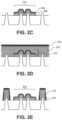
- a patterning process e.g., a lithography and etch process, of the silicon nitride hardmask 310 is performed to provide a resistor mask 311.
- a second layer of polysilicon 314 is then formed above the resistor mask 311.
- the second layer of polysilicon 314 is planarized, e.g., by a chemical mechanical polishing process, and a second hardmask layer 316 is formed thereon, as depicted in Figure 3D .
- a patterning process e.g., a lithography and etch process, of the first layer of polysilicon 308, the second layer of polysilicon 314, and the second hardmask 316 is performed to provide dummy gate structures 318, which may include spacers 320, and to provide resistor structure 312.
- the dummy gate structure 318 may then be masked by mask 322 and an implant process 324 is performed to resistor structure 312, as depicted in Figure 3F , e.g., to provide desired resistance characteristics for resistor structure 312.
- the recessing 423 in one embodiment, involved removal of the hardmask as well as a portion of the polysilicon layer.
- An implant process 424 is performed to resistor structure 412, as depicted in Figure 4F , e.g., to provide desired resistance characteristics for resistor structure 412.
- mask 422 is removed and an inter-layer dielectric layer 426 (e.g., silicon oxide) is formed over the dummy gate structures 418 and the resistor structure 412.
- the inter-layer dielectric layer 426 is planarized to expose the polysilicon of the dummy gate structure 418, but to retain resistor structure 412 as un-exposed.
- the photoresist layer 560 is removed and the undoped portion of the polysilicon layer 508 are removed, e.g., by a selective wet etch process such as tetramethylammonium hydroxide (TMAH).
- TMAH tetramethylammonium hydroxide
- the remaining doped polysilicon region 562 may subsequently be used to form a precision resistor.
- the above approach may be referred to as a selectively implanted polysilicon resistor approach.
- Figures 6A-6L illustrate cross-sectional views representing various operations in another method of fabricating a precision resistor for a non-planar semiconductor device architecture, in accordance with an embodiment of the present invention.
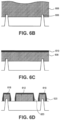
- an isolation layer 602 is formed on a patterned bulk substrate 604 and recessed to leave a plurality of fins 606 exposed.
- a layer of polysilicon 608 is then formed above the fins 606, as depicted in Figure 6B .
- an insulating layer may first be formed on fins 606 to ultimately insulate polysilicon layer 608 from the fin material.
- the plurality of dummy gates is removed by a dry etch or wet etch process.
- the plurality of dummy gates is composed of polycrystalline silicon or amorphous silicon and is removed with a dry etch process comprising SF6.
- the plurality of dummy gates is composed of polycrystalline silicon or amorphous silicon and is removed with a wet etch process comprising aqueous NH40H or tetramethylammonium hydroxide.
- the plurality of dummy gates is composed of silicon nitride and is removed with a wet etch comprising aqueous phosphoric acid.
- one or more embodiments of the present invention may be directed to a gate aligned contact process.
- a process may be implemented to form contact structures for semiconductor structure fabrication, e.g., for integrated circuit fabrication.
- a contact pattern is formed as aligned to an existing gate pattern.
- conventional approaches typically involve an additional lithography process with tight registration of a lithographic contact pattern to an existing gate pattern in combination with selective contact etches.
- a conventional process may include patterning of a poly (gate) grid with separately patterning of contacts and contact plugs.
- a plot 700 is provided to demonstrate the variation of presently described precision resistors versus their tungsten trench counterparts, in accordance with an embodiment.
- present resistors EPR
- TCN tungsten trench resistors
- the resistor structure is a non-planar resistor structure.
- the resistive material layer has a top surface at a height less than the heights of the first and second semiconductor fins.
Landscapes
- Semiconductor Integrated Circuits (AREA)
- Metal-Oxide And Bipolar Metal-Oxide Semiconductor Integrated Circuits (AREA)
Applications Claiming Priority (4)
| Application Number | Priority Date | Filing Date | Title |
|---|---|---|---|
| US13/625,698 US8796772B2 (en) | 2012-09-24 | 2012-09-24 | Precision resistor for non-planar semiconductor device architecture |
| EP17191534.1A EP3285300A1 (de) | 2012-09-24 | 2013-06-18 | Präzisionswiderstand für eine nichtplanare halbleiterbauelementarchitektur |
| EP13839477.0A EP2898533B1 (de) | 2012-09-24 | 2013-06-18 | Präzisionswiderstand für eine nichtplanare halbleiterbauelemente-architektur |
| PCT/US2013/046395 WO2014046755A1 (en) | 2012-09-24 | 2013-06-18 | Precision resistor for non-planar semiconductor device architecture |
Related Parent Applications (3)
| Application Number | Title | Priority Date | Filing Date |
|---|---|---|---|
| EP17191534.1A Division EP3285300A1 (de) | 2012-09-24 | 2013-06-18 | Präzisionswiderstand für eine nichtplanare halbleiterbauelementarchitektur |
| EP13839477.0A Division-Into EP2898533B1 (de) | 2012-09-24 | 2013-06-18 | Präzisionswiderstand für eine nichtplanare halbleiterbauelemente-architektur |
| EP13839477.0A Division EP2898533B1 (de) | 2012-09-24 | 2013-06-18 | Präzisionswiderstand für eine nichtplanare halbleiterbauelemente-architektur |
Publications (2)
| Publication Number | Publication Date |
|---|---|
| EP4283676A2 true EP4283676A2 (de) | 2023-11-29 |
| EP4283676A3 EP4283676A3 (de) | 2024-07-17 |
Family
ID=50338031
Family Applications (4)
| Application Number | Title | Priority Date | Filing Date |
|---|---|---|---|
| EP17191534.1A Pending EP3285300A1 (de) | 2012-09-24 | 2013-06-18 | Präzisionswiderstand für eine nichtplanare halbleiterbauelementarchitektur |
| EP23193624.6A Pending EP4283676A3 (de) | 2012-09-24 | 2013-06-18 | Präzisionswiderstand für eine nichtplanare halbleiterbauelementarchitektur |
| EP13839477.0A Active EP2898533B1 (de) | 2012-09-24 | 2013-06-18 | Präzisionswiderstand für eine nichtplanare halbleiterbauelemente-architektur |
| EP17152588.4A Ceased EP3182452A1 (de) | 2012-09-24 | 2013-06-18 | Präzisionswiderstand für eine nichtplanare halbleiterbauelementearchitektur |
Family Applications Before (1)
| Application Number | Title | Priority Date | Filing Date |
|---|---|---|---|
| EP17191534.1A Pending EP3285300A1 (de) | 2012-09-24 | 2013-06-18 | Präzisionswiderstand für eine nichtplanare halbleiterbauelementarchitektur |
Family Applications After (2)
| Application Number | Title | Priority Date | Filing Date |
|---|---|---|---|
| EP13839477.0A Active EP2898533B1 (de) | 2012-09-24 | 2013-06-18 | Präzisionswiderstand für eine nichtplanare halbleiterbauelemente-architektur |
| EP17152588.4A Ceased EP3182452A1 (de) | 2012-09-24 | 2013-06-18 | Präzisionswiderstand für eine nichtplanare halbleiterbauelementearchitektur |
Country Status (6)
| Country | Link |
|---|---|
| US (2) | US8796772B2 (de) |
| EP (4) | EP3285300A1 (de) |
| KR (3) | KR101969243B1 (de) |
| CN (4) | CN106971978B (de) |
| TW (4) | TWI552311B (de) |
| WO (1) | WO2014046755A1 (de) |
Families Citing this family (37)
| Publication number | Priority date | Publication date | Assignee | Title |
|---|---|---|---|---|
| US8962421B2 (en) * | 2012-11-15 | 2015-02-24 | GlobalFoundries, Inc. | Methods for fabricating integrated circuits including semiconductive resistor structures in a FinFET architecture |
| US9196542B2 (en) * | 2013-05-22 | 2015-11-24 | United Microelectronics Corp. | Method for manufacturing semiconductor devices |
| US9941271B2 (en) | 2013-10-04 | 2018-04-10 | Avago Technologies General Ip (Singapore) Pte. Ltd. | Fin-shaped field effect transistor and capacitor structures |
| US9490176B2 (en) * | 2014-10-17 | 2016-11-08 | Taiwan Semiconductor Manufacturing Company, Ltd. | Method and structure for FinFET isolation |
| US9685434B2 (en) | 2014-12-10 | 2017-06-20 | International Business Machines Corporation | Inter-level dielectric layer in replacement metal gates and resistor fabrication |
| TWI620358B (zh) * | 2015-01-28 | 2018-04-01 | 旺宏電子股份有限公司 | 記憶體結構及其製造方法 |
| US9514998B1 (en) | 2015-05-11 | 2016-12-06 | International Business Machines Corporation | Polysilicon resistor formation in silicon-on-insulator replacement metal gate finFET processes |
| WO2017034555A1 (en) * | 2015-08-26 | 2017-03-02 | Intel Corporation | Compound lateral resistor structures for integrated circuitry |
| WO2017052626A1 (en) * | 2015-09-25 | 2017-03-30 | Intel Corporation | Power gate with metal on both sides |
| US9570571B1 (en) | 2015-11-18 | 2017-02-14 | International Business Machines Corporation | Gate stack integrated metal resistors |
| WO2017099792A1 (en) * | 2015-12-11 | 2017-06-15 | Intel Corporation | Metal-oxide-polysilicon tunable resistor for flexible circuit design and method of fabricating same |
| WO2017111771A1 (en) * | 2015-12-23 | 2017-06-29 | Intel Corporation | Thin film polysilicon resistor by gate-to-gate isolation |
| CN106935504B (zh) * | 2015-12-30 | 2019-11-01 | 中芯国际集成电路制造(上海)有限公司 | 半导体结构及其形成方法 |
| WO2018004672A1 (en) * | 2016-07-01 | 2018-01-04 | Intel Corporation | Thin film resistor with reduced capacitance |
| CN107677386B (zh) * | 2016-08-02 | 2019-07-26 | 中芯国际集成电路制造(上海)有限公司 | 用于温度测量的半导体结构和温度测量方法 |
| US10002868B2 (en) | 2016-09-30 | 2018-06-19 | International Business Machines Corporation | Vertical fin resistor devices |
| US10930729B2 (en) | 2016-10-21 | 2021-02-23 | Intel Corporation | Fin-based thin film resistor |
| US9954050B1 (en) | 2016-10-24 | 2018-04-24 | International Business Machines Corporation | Precise/designable FinFET resistor structure |
| US9997590B2 (en) | 2016-10-24 | 2018-06-12 | International Büsiness Machines Corporation | FinFET resistor and method to fabricate same |
| US10872889B2 (en) * | 2016-11-17 | 2020-12-22 | Taiwan Semiconductor Manufacturing Co., Ltd. | Semiconductor component and fabricating method thereof |
| US10411085B2 (en) | 2016-12-29 | 2019-09-10 | Taiwan Semiconductor Manufacturing Co., Ltd. | Semiconductor device and a method for fabricating the same |
| US10840354B2 (en) * | 2017-02-06 | 2020-11-17 | International Business Machines Corporation | Approach to bottom dielectric isolation for vertical transport fin field effect transistors |
| US10056469B1 (en) * | 2017-02-13 | 2018-08-21 | Globalfoundries Inc. | Gate cut integration and related device |
| US10074575B1 (en) | 2017-06-21 | 2018-09-11 | International Business Machines Corporation | Integrating and isolating nFET and pFET nanosheet transistors on a substrate |
| US10770302B2 (en) * | 2018-09-27 | 2020-09-08 | Taiwan Semiconductor Manufacturing Company, Ltd. | Semiconductor FinFET device and method |
| DE102019104629B4 (de) | 2018-09-27 | 2022-10-20 | Taiwan Semiconductor Manufacturing Co., Ltd. | FinFET-Halbleiter-Bauelement und Verfahren |
| US11056537B2 (en) | 2019-03-27 | 2021-07-06 | International Business Machines Corporation | Self-aligned gate contact integration with metal resistor |
| US11233117B2 (en) | 2019-10-31 | 2022-01-25 | Taiwan Semiconductor Manufacturing Company, Ltd. | Ring structure for film resistor |
| JP7556682B2 (ja) | 2019-10-31 | 2024-09-26 | ソニーセミコンダクタソリューションズ株式会社 | 電子機器 |
| KR102863746B1 (ko) | 2019-11-26 | 2025-09-24 | 삼성전자주식회사 | 반도체 장치 |
| KR102771900B1 (ko) | 2019-12-09 | 2025-02-25 | 삼성전자주식회사 | 도핑 영역을 갖는 저항 소자 |
| US11637173B2 (en) * | 2020-09-29 | 2023-04-25 | Globalfoundries U.S. Inc. | Structure including polycrystalline resistor with dopant-including polycrystalline region thereunder |
| US20220238516A1 (en) * | 2021-01-25 | 2022-07-28 | Yanbiao Pan | Polysilicon resistor using reduced grain size polysilicon |
| US12495545B2 (en) | 2022-06-10 | 2025-12-09 | Fujian Jinhua Integrated Circuit Co., Ltd. | Semiconductor memory device and method of fabricating the same |
| US12426242B2 (en) | 2022-09-01 | 2025-09-23 | Fujian Jinhua Integrated Circuit Co., Ltd. | Semiconductor memory device having a bit line contact disposed in the substrate |
| CN116799004B (zh) * | 2023-08-23 | 2023-11-28 | 合肥晶合集成电路股份有限公司 | 一种半导体集成器件及其制作方法 |
| TWI890603B (zh) * | 2024-10-17 | 2025-07-11 | 聯華電子股份有限公司 | 半導體元件及其製作方法 |
Family Cites Families (36)
| Publication number | Priority date | Publication date | Assignee | Title |
|---|---|---|---|---|
| US4467519A (en) * | 1982-04-01 | 1984-08-28 | International Business Machines Corporation | Process for fabricating polycrystalline silicon film resistors |
| TW478050B (en) * | 2001-03-21 | 2002-03-01 | Taiwan Semiconductor Mfg | Method of fabricating polysilicon resistor on metal gate |
| US6803680B2 (en) * | 2002-09-13 | 2004-10-12 | Mia-Com, Inc. | Apparatus, methods, and articles of manufacture for a switch having sharpened control voltage |
| US7173305B2 (en) * | 2003-04-08 | 2007-02-06 | Taiwan Semiconductor Manufacturing Company, Ltd. | Self-aligned contact for silicon-on-insulator devices |
| KR100618827B1 (ko) * | 2004-05-17 | 2006-09-08 | 삼성전자주식회사 | FinFET을 포함하는 반도체 소자 및 그 제조방법 |
| US7397087B2 (en) * | 2004-08-06 | 2008-07-08 | International Business Machines Corporation | FEOL/MEOL metal resistor for high end CMOS |
| US7227183B2 (en) * | 2004-09-17 | 2007-06-05 | International Business Machines Corporation | Polysilicon conductor width measurement for 3-dimensional FETs |
| TWI267951B (en) * | 2004-09-30 | 2006-12-01 | Taiwan Semiconductor Mfg | A device having multiple silicide types and a method for its fabrication |
| US20070018239A1 (en) | 2005-07-20 | 2007-01-25 | International Business Machines Corporation | Sea-of-fins structure on a semiconductor substrate and method of fabrication |
| US7479421B2 (en) * | 2005-09-28 | 2009-01-20 | Intel Corporation | Process for integrating planar and non-planar CMOS transistors on a bulk substrate and article made thereby |
| US8174073B2 (en) * | 2007-05-30 | 2012-05-08 | Taiwan Semiconductor Manufacturing Co., Ltd. | Integrated circuit structures with multiple FinFETs |
| US7994020B2 (en) * | 2008-07-21 | 2011-08-09 | Advanced Micro Devices, Inc. | Method of forming finned semiconductor devices with trench isolation |
| US7879666B2 (en) * | 2008-07-23 | 2011-02-01 | Freescale Semiconductor, Inc. | Semiconductor resistor formed in metal gate stack |
| US20100059823A1 (en) * | 2008-09-10 | 2010-03-11 | Taiwan Semiconductor Manufacturing Company, Ltd. | Resistive device for high-k metal gate technology and method of making |
| US8138037B2 (en) * | 2009-03-17 | 2012-03-20 | International Business Machines Corporation | Method and structure for gate height scaling with high-k/metal gate technology |
| US7955928B2 (en) * | 2009-03-30 | 2011-06-07 | International Business Machines Corporation | Structure and method of fabricating FinFET |
| US7960282B2 (en) * | 2009-05-21 | 2011-06-14 | Globalfoundries Singapore Pte. Ltd. | Method of manufacture an integrated circuit system with through silicon via |
| US8053809B2 (en) * | 2009-05-26 | 2011-11-08 | International Business Machines Corporation | Device including high-K metal gate finfet and resistive structure and method of forming thereof |
| US8193900B2 (en) * | 2009-06-24 | 2012-06-05 | United Microelectronics Corp. | Method for fabricating metal gate and polysilicon resistor and related polysilicon resistor structure |
| US8980719B2 (en) * | 2010-04-28 | 2015-03-17 | Taiwan Semiconductor Manufacturing Company, Ltd. | Methods for doping fin field-effect transistors |
| US8890260B2 (en) * | 2009-09-04 | 2014-11-18 | Taiwan Semiconductor Manufacturing Company, Ltd. | Polysilicon design for replacement gate technology |
| US7985639B2 (en) * | 2009-09-18 | 2011-07-26 | GlobalFoundries, Inc. | Method for fabricating a semiconductor device having a semiconductive resistor structure |
| US7993999B2 (en) * | 2009-11-09 | 2011-08-09 | International Business Machines Corporation | High-K/metal gate CMOS finFET with improved pFET threshold voltage |
| US20110147831A1 (en) * | 2009-12-23 | 2011-06-23 | Steigerwald Joseph M | Method for replacement metal gate fill |
| US8389359B2 (en) * | 2010-02-08 | 2013-03-05 | Taiwan Semiconductor Manufacturing Company, Ltd. | Method for forming low resistance and uniform metal gate |
| JP2011181841A (ja) * | 2010-03-03 | 2011-09-15 | Toshiba Corp | 半導体装置の製造方法 |
| US8546228B2 (en) * | 2010-06-16 | 2013-10-01 | International Business Machines Corporation | Strained thin body CMOS device having vertically raised source/drain stressors with single spacer |
| US8278173B2 (en) * | 2010-06-30 | 2012-10-02 | Taiwan Semiconductor Manufacturing Company, Ltd. | Method of fabricating gate structures |
| US8058125B1 (en) * | 2010-08-04 | 2011-11-15 | Taiwan Semiconductor Manufacturing Company, Ltd. | Poly resistor on a semiconductor device |
| US9385050B2 (en) * | 2011-01-06 | 2016-07-05 | Globalfoundries Inc. | Structure and method to fabricate resistor on finFET processes |
| US9269758B2 (en) * | 2011-01-13 | 2016-02-23 | Taiwan Semiconductor Manufacturing Company, Ltd. | Low TCR high resistance resistor |
| US9293584B2 (en) * | 2011-11-02 | 2016-03-22 | Broadcom Corporation | FinFET devices |
| US9087687B2 (en) * | 2011-12-23 | 2015-07-21 | International Business Machines Corporation | Thin heterostructure channel device |
| US8569127B2 (en) * | 2012-03-13 | 2013-10-29 | United Microelectronics Corp. | Semiconductor device and method for fabricating the same |
| US8816436B2 (en) * | 2012-05-16 | 2014-08-26 | International Business Machines Corporation | Method and structure for forming fin resistors |
| US9093556B2 (en) * | 2012-08-21 | 2015-07-28 | Stmicroelectronics, Inc. | Multi-fin FINFET device including epitaxial growth barrier on outside surfaces of outermost fins and related methods |
-
2012
- 2012-09-24 US US13/625,698 patent/US8796772B2/en active Active
-
2013
- 2013-06-18 EP EP17191534.1A patent/EP3285300A1/de active Pending
- 2013-06-18 CN CN201710067644.6A patent/CN106971978B/zh active Active
- 2013-06-18 CN CN201380042912.9A patent/CN104541377B/zh active Active
- 2013-06-18 KR KR1020177003659A patent/KR101969243B1/ko active Active
- 2013-06-18 WO PCT/US2013/046395 patent/WO2014046755A1/en not_active Ceased
- 2013-06-18 KR KR1020157001592A patent/KR101707754B1/ko active Active
- 2013-06-18 EP EP23193624.6A patent/EP4283676A3/de active Pending
- 2013-06-18 CN CN201710228504.2A patent/CN107256858B/zh active Active
- 2013-06-18 EP EP13839477.0A patent/EP2898533B1/de active Active
- 2013-06-18 KR KR1020177009819A patent/KR101969246B1/ko active Active
- 2013-06-18 CN CN201910635550.3A patent/CN110400801B/zh active Active
- 2013-06-18 EP EP17152588.4A patent/EP3182452A1/de not_active Ceased
- 2013-09-04 TW TW104108118A patent/TWI552311B/zh active
- 2013-09-04 TW TW102131802A patent/TWI487116B/zh active
- 2013-09-04 TW TW106110332A patent/TWI623082B/zh active
- 2013-09-04 TW TW105123243A patent/TWI610419B/zh active
-
2014
- 2014-06-24 US US14/313,678 patent/US8889508B2/en active Active
Also Published As
| Publication number | Publication date |
|---|---|
| TWI623082B (zh) | 2018-05-01 |
| EP2898533B1 (de) | 2024-07-10 |
| TW201539712A (zh) | 2015-10-16 |
| US20140308785A1 (en) | 2014-10-16 |
| CN110400801B (zh) | 2024-03-01 |
| EP2898533A4 (de) | 2016-08-31 |
| CN106971978B (zh) | 2021-03-12 |
| US20140084381A1 (en) | 2014-03-27 |
| KR20150034188A (ko) | 2015-04-02 |
| TWI610419B (zh) | 2018-01-01 |
| TW201727871A (zh) | 2017-08-01 |
| KR20170042826A (ko) | 2017-04-19 |
| WO2014046755A1 (en) | 2014-03-27 |
| KR101707754B1 (ko) | 2017-02-16 |
| KR101969243B1 (ko) | 2019-04-15 |
| CN110400801A (zh) | 2019-11-01 |
| US8889508B2 (en) | 2014-11-18 |
| EP3285300A1 (de) | 2018-02-21 |
| EP2898533A1 (de) | 2015-07-29 |
| EP3182452A1 (de) | 2017-06-21 |
| CN104541377B (zh) | 2019-08-20 |
| KR101969246B1 (ko) | 2019-04-15 |
| CN107256858B (zh) | 2020-11-10 |
| TWI552311B (zh) | 2016-10-01 |
| EP4283676A3 (de) | 2024-07-17 |
| CN107256858A (zh) | 2017-10-17 |
| TW201432908A (zh) | 2014-08-16 |
| TWI487116B (zh) | 2015-06-01 |
| US8796772B2 (en) | 2014-08-05 |
| KR20170018478A (ko) | 2017-02-17 |
| CN104541377A (zh) | 2015-04-22 |
| CN106971978A (zh) | 2017-07-21 |
| TW201709480A (zh) | 2017-03-01 |
Similar Documents
| Publication | Publication Date | Title |
|---|---|---|
| US8889508B2 (en) | Precision resistor for non-planar semiconductor device architecture | |
| US10263112B2 (en) | Vertical non-planar semiconductor device for system-on-chip (SoC) applications | |
| US9881927B2 (en) | CMOS-compatible polycide fuse structure and method of fabricating same | |
| EP3425675B1 (de) | Nichtplanares halbleiterbauelement mit omega-lamelle mit dotiertem unterlamellenbereich | |
| CN105431929B (zh) | 具有掺杂的子鳍片区域的非平面半导体器件及其制造方法 | |
| CN107039281B (zh) | 具有颈状半导体主体的半导体器件以及形成不同宽度的半导体主体的方法 |
Legal Events
| Date | Code | Title | Description |
|---|---|---|---|
| PUAI | Public reference made under article 153(3) epc to a published international application that has entered the european phase |
Free format text: ORIGINAL CODE: 0009012 |
|
| STAA | Information on the status of an ep patent application or granted ep patent |
Free format text: STATUS: REQUEST FOR EXAMINATION WAS MADE |
|
| 17P | Request for examination filed |
Effective date: 20230828 |
|
| AC | Divisional application: reference to earlier application |
Ref document number: 2898533 Country of ref document: EP Kind code of ref document: P Ref document number: 3285300 Country of ref document: EP Kind code of ref document: P |
|
| AK | Designated contracting states |
Kind code of ref document: A2 Designated state(s): AL AT BE BG CH CY CZ DE DK EE ES FI FR GB GR HR HU IE IS IT LI LT LU LV MC MK MT NL NO PL PT RO RS SE SI SK SM TR |
|
| PUAL | Search report despatched |
Free format text: ORIGINAL CODE: 0009013 |
|
| AK | Designated contracting states |
Kind code of ref document: A3 Designated state(s): AL AT BE BG CH CY CZ DE DK EE ES FI FR GB GR HR HU IE IS IT LI LT LU LV MC MK MT NL NO PL PT RO RS SE SI SK SM TR |
|
| RIC1 | Information provided on ipc code assigned before grant |
Ipc: H01L 21/8234 20060101ALN20240607BHEP Ipc: H01L 29/66 20060101ALN20240607BHEP Ipc: H01L 27/088 20060101ALN20240607BHEP Ipc: H10N 97/00 20230101ALI20240607BHEP Ipc: H01L 27/06 20060101AFI20240607BHEP |