EP4283676A2 - Precision resistor for non-planar semiconductor device architecture - Google Patents
Precision resistor for non-planar semiconductor device architecture Download PDFInfo
- Publication number
- EP4283676A2 EP4283676A2 EP23193624.6A EP23193624A EP4283676A2 EP 4283676 A2 EP4283676 A2 EP 4283676A2 EP 23193624 A EP23193624 A EP 23193624A EP 4283676 A2 EP4283676 A2 EP 4283676A2
- Authority
- EP
- European Patent Office
- Prior art keywords
- fin
- resistor
- layer
- semiconductor
- gate
- Prior art date
- Legal status (The legal status is an assumption and is not a legal conclusion. Google has not performed a legal analysis and makes no representation as to the accuracy of the status listed.)
- Pending
Links
- 239000004065 semiconductor Substances 0.000 title claims abstract description 110
- 239000000758 substrate Substances 0.000 claims abstract description 41
- 238000002955 isolation Methods 0.000 claims abstract description 24
- 239000000463 material Substances 0.000 claims description 54
- 229910052710 silicon Inorganic materials 0.000 claims description 24
- 239000010703 silicon Substances 0.000 claims description 24
- WFKWXMTUELFFGS-UHFFFAOYSA-N tungsten Chemical compound [W] WFKWXMTUELFFGS-UHFFFAOYSA-N 0.000 claims description 21
- 229910052721 tungsten Inorganic materials 0.000 claims description 21
- 239000010937 tungsten Substances 0.000 claims description 21
- VYPSYNLAJGMNEJ-UHFFFAOYSA-N Silicium dioxide Chemical compound O=[Si]=O VYPSYNLAJGMNEJ-UHFFFAOYSA-N 0.000 claims description 20
- 229910052814 silicon oxide Inorganic materials 0.000 claims description 12
- 229910000449 hafnium oxide Inorganic materials 0.000 claims description 8
- WIHZLLGSGQNAGK-UHFFFAOYSA-N hafnium(4+);oxygen(2-) Chemical compound [O-2].[O-2].[Hf+4] WIHZLLGSGQNAGK-UHFFFAOYSA-N 0.000 claims description 8
- RTAQQCXQSZGOHL-UHFFFAOYSA-N Titanium Chemical compound [Ti] RTAQQCXQSZGOHL-UHFFFAOYSA-N 0.000 claims description 2
- 229910052719 titanium Inorganic materials 0.000 claims description 2
- 239000010936 titanium Substances 0.000 claims description 2
- 239000010410 layer Substances 0.000 description 113
- 229910021420 polycrystalline silicon Inorganic materials 0.000 description 95
- 229910052751 metal Inorganic materials 0.000 description 77
- 239000002184 metal Substances 0.000 description 77
- 229920005591 polysilicon Polymers 0.000 description 74
- 238000000034 method Methods 0.000 description 68
- 230000008569 process Effects 0.000 description 57
- 238000004519 manufacturing process Methods 0.000 description 28
- XUIMIQQOPSSXEZ-UHFFFAOYSA-N Silicon Chemical compound [Si] XUIMIQQOPSSXEZ-UHFFFAOYSA-N 0.000 description 23
- 238000013459 approach Methods 0.000 description 21
- 238000004891 communication Methods 0.000 description 15
- 229910052581 Si3N4 Inorganic materials 0.000 description 14
- 239000011810 insulating material Substances 0.000 description 14
- HQVNEWCFYHHQES-UHFFFAOYSA-N silicon nitride Chemical compound N12[Si]34N5[Si]62N3[Si]51N64 HQVNEWCFYHHQES-UHFFFAOYSA-N 0.000 description 14
- 229910052723 transition metal Inorganic materials 0.000 description 12
- 239000011229 interlayer Substances 0.000 description 11
- 239000003989 dielectric material Substances 0.000 description 10
- 238000005516 engineering process Methods 0.000 description 9
- 229910052735 hafnium Inorganic materials 0.000 description 9
- VBJZVLUMGGDVMO-UHFFFAOYSA-N hafnium atom Chemical compound [Hf] VBJZVLUMGGDVMO-UHFFFAOYSA-N 0.000 description 9
- 150000003624 transition metals Chemical class 0.000 description 9
- 230000010354 integration Effects 0.000 description 8
- 238000000059 patterning Methods 0.000 description 8
- 125000006850 spacer group Chemical group 0.000 description 8
- 238000001459 lithography Methods 0.000 description 7
- ZOXJGFHDIHLPTG-UHFFFAOYSA-N Boron Chemical compound [B] ZOXJGFHDIHLPTG-UHFFFAOYSA-N 0.000 description 6
- 230000015572 biosynthetic process Effects 0.000 description 6
- 229910052796 boron Inorganic materials 0.000 description 6
- 239000007943 implant Substances 0.000 description 6
- WGTYBPLFGIVFAS-UHFFFAOYSA-M tetramethylammonium hydroxide Chemical compound [OH-].C[N+](C)(C)C WGTYBPLFGIVFAS-UHFFFAOYSA-M 0.000 description 6
- -1 transition metal nitride Chemical class 0.000 description 6
- 238000005498 polishing Methods 0.000 description 5
- PXHVJJICTQNCMI-UHFFFAOYSA-N Nickel Chemical compound [Ni] PXHVJJICTQNCMI-UHFFFAOYSA-N 0.000 description 4
- QVGXLLKOCUKJST-UHFFFAOYSA-N atomic oxygen Chemical compound [O] QVGXLLKOCUKJST-UHFFFAOYSA-N 0.000 description 4
- 238000013461 design Methods 0.000 description 4
- 229910052732 germanium Inorganic materials 0.000 description 4
- GNPVGFCGXDBREM-UHFFFAOYSA-N germanium atom Chemical compound [Ge] GNPVGFCGXDBREM-UHFFFAOYSA-N 0.000 description 4
- 229910052760 oxygen Inorganic materials 0.000 description 4
- 239000001301 oxygen Substances 0.000 description 4
- 238000012545 processing Methods 0.000 description 4
- 230000000717 retained effect Effects 0.000 description 4
- 229910021332 silicide Inorganic materials 0.000 description 4
- 235000012239 silicon dioxide Nutrition 0.000 description 4
- 239000000377 silicon dioxide Substances 0.000 description 4
- 239000000126 substance Substances 0.000 description 4
- 229910000951 Aluminide Inorganic materials 0.000 description 3
- 229910052782 aluminium Inorganic materials 0.000 description 3
- XAGFODPZIPBFFR-UHFFFAOYSA-N aluminium Chemical compound [Al] XAGFODPZIPBFFR-UHFFFAOYSA-N 0.000 description 3
- 238000000151 deposition Methods 0.000 description 3
- 230000008021 deposition Effects 0.000 description 3
- 239000012212 insulator Substances 0.000 description 3
- 230000001681 protective effect Effects 0.000 description 3
- FVBUAEGBCNSCDD-UHFFFAOYSA-N silicide(4-) Chemical compound [Si-4] FVBUAEGBCNSCDD-UHFFFAOYSA-N 0.000 description 3
- 229910005540 GaP Inorganic materials 0.000 description 2
- KDLHZDBZIXYQEI-UHFFFAOYSA-N Palladium Chemical compound [Pd] KDLHZDBZIXYQEI-UHFFFAOYSA-N 0.000 description 2
- NBIIXXVUZAFLBC-UHFFFAOYSA-N Phosphoric acid Chemical compound OP(O)(O)=O NBIIXXVUZAFLBC-UHFFFAOYSA-N 0.000 description 2
- 229910045601 alloy Inorganic materials 0.000 description 2
- 239000000956 alloy Substances 0.000 description 2
- 229910021417 amorphous silicon Inorganic materials 0.000 description 2
- 230000006399 behavior Effects 0.000 description 2
- 239000002800 charge carrier Substances 0.000 description 2
- 229910017052 cobalt Inorganic materials 0.000 description 2
- 239000010941 cobalt Substances 0.000 description 2
- GUTLYIVDDKVIGB-UHFFFAOYSA-N cobalt atom Chemical compound [Co] GUTLYIVDDKVIGB-UHFFFAOYSA-N 0.000 description 2
- 230000009977 dual effect Effects 0.000 description 2
- HZXMRANICFIONG-UHFFFAOYSA-N gallium phosphide Chemical compound [Ga]#P HZXMRANICFIONG-UHFFFAOYSA-N 0.000 description 2
- MRELNEQAGSRDBK-UHFFFAOYSA-N lanthanum(3+);oxygen(2-) Chemical compound [O-2].[O-2].[O-2].[La+3].[La+3] MRELNEQAGSRDBK-UHFFFAOYSA-N 0.000 description 2
- 229910052759 nickel Inorganic materials 0.000 description 2
- RUFLMLWJRZAWLJ-UHFFFAOYSA-N nickel silicide Chemical group [Ni]=[Si]=[Ni] RUFLMLWJRZAWLJ-UHFFFAOYSA-N 0.000 description 2
- 229910021334 nickel silicide Inorganic materials 0.000 description 2
- 229920002120 photoresistant polymer Polymers 0.000 description 2
- BASFCYQUMIYNBI-UHFFFAOYSA-N platinum Chemical compound [Pt] BASFCYQUMIYNBI-UHFFFAOYSA-N 0.000 description 2
- 238000007517 polishing process Methods 0.000 description 2
- JBRZTFJDHDCESZ-UHFFFAOYSA-N AsGa Chemical compound [As]#[Ga] JBRZTFJDHDCESZ-UHFFFAOYSA-N 0.000 description 1
- OKTJSMMVPCPJKN-UHFFFAOYSA-N Carbon Chemical compound [C] OKTJSMMVPCPJKN-UHFFFAOYSA-N 0.000 description 1
- 229910002601 GaN Inorganic materials 0.000 description 1
- 229910001218 Gallium arsenide Inorganic materials 0.000 description 1
- 229910000530 Gallium indium arsenide Inorganic materials 0.000 description 1
- JMASRVWKEDWRBT-UHFFFAOYSA-N Gallium nitride Chemical compound [Ga]#N JMASRVWKEDWRBT-UHFFFAOYSA-N 0.000 description 1
- GPXJNWSHGFTCBW-UHFFFAOYSA-N Indium phosphide Chemical compound [In]#P GPXJNWSHGFTCBW-UHFFFAOYSA-N 0.000 description 1
- 229910017974 NH40H Inorganic materials 0.000 description 1
- BPQQTUXANYXVAA-UHFFFAOYSA-N Orthosilicate Chemical compound [O-][Si]([O-])([O-])[O-] BPQQTUXANYXVAA-UHFFFAOYSA-N 0.000 description 1
- OAICVXFJPJFONN-UHFFFAOYSA-N Phosphorus Chemical compound [P] OAICVXFJPJFONN-UHFFFAOYSA-N 0.000 description 1
- KJTLSVCANCCWHF-UHFFFAOYSA-N Ruthenium Chemical compound [Ru] KJTLSVCANCCWHF-UHFFFAOYSA-N 0.000 description 1
- BUGBHKTXTAQXES-UHFFFAOYSA-N Selenium Chemical compound [Se] BUGBHKTXTAQXES-UHFFFAOYSA-N 0.000 description 1
- 229910000577 Silicon-germanium Inorganic materials 0.000 description 1
- NINIDFKCEFEMDL-UHFFFAOYSA-N Sulfur Chemical compound [S] NINIDFKCEFEMDL-UHFFFAOYSA-N 0.000 description 1
- QCWXUUIWCKQGHC-UHFFFAOYSA-N Zirconium Chemical compound [Zr] QCWXUUIWCKQGHC-UHFFFAOYSA-N 0.000 description 1
- KXNLCSXBJCPWGL-UHFFFAOYSA-N [Ga].[As].[In] Chemical compound [Ga].[As].[In] KXNLCSXBJCPWGL-UHFFFAOYSA-N 0.000 description 1
- XWCMFHPRATWWFO-UHFFFAOYSA-N [O-2].[Ta+5].[Sc+3].[O-2].[O-2].[O-2] Chemical compound [O-2].[Ta+5].[Sc+3].[O-2].[O-2].[O-2] XWCMFHPRATWWFO-UHFFFAOYSA-N 0.000 description 1
- LEVVHYCKPQWKOP-UHFFFAOYSA-N [Si].[Ge] Chemical compound [Si].[Ge] LEVVHYCKPQWKOP-UHFFFAOYSA-N 0.000 description 1
- FTWRSWRBSVXQPI-UHFFFAOYSA-N alumanylidynearsane;gallanylidynearsane Chemical compound [As]#[Al].[As]#[Ga] FTWRSWRBSVXQPI-UHFFFAOYSA-N 0.000 description 1
- 229910000147 aluminium phosphate Inorganic materials 0.000 description 1
- 229910052785 arsenic Inorganic materials 0.000 description 1
- RQNWIZPPADIBDY-UHFFFAOYSA-N arsenic atom Chemical compound [As] RQNWIZPPADIBDY-UHFFFAOYSA-N 0.000 description 1
- 229910052454 barium strontium titanate Inorganic materials 0.000 description 1
- JRPBQTZRNDNNOP-UHFFFAOYSA-N barium titanate Chemical compound [Ba+2].[Ba+2].[O-][Ti]([O-])([O-])[O-] JRPBQTZRNDNNOP-UHFFFAOYSA-N 0.000 description 1
- 229910002113 barium titanate Inorganic materials 0.000 description 1
- 230000000903 blocking effect Effects 0.000 description 1
- 229910052799 carbon Inorganic materials 0.000 description 1
- 230000008859 change Effects 0.000 description 1
- 238000005229 chemical vapour deposition Methods 0.000 description 1
- 150000001875 compounds Chemical class 0.000 description 1
- 239000013078 crystal Substances 0.000 description 1
- 229910021419 crystalline silicon Inorganic materials 0.000 description 1
- 238000009792 diffusion process Methods 0.000 description 1
- 239000002019 doping agent Substances 0.000 description 1
- 239000007772 electrode material Substances 0.000 description 1
- 230000005670 electromagnetic radiation Effects 0.000 description 1
- 230000005669 field effect Effects 0.000 description 1
- 230000006870 function Effects 0.000 description 1
- 239000012535 impurity Substances 0.000 description 1
- 238000010348 incorporation Methods 0.000 description 1
- 229910052738 indium Inorganic materials 0.000 description 1
- WPYVAWXEWQSOGY-UHFFFAOYSA-N indium antimonide Chemical compound [Sb]#[In] WPYVAWXEWQSOGY-UHFFFAOYSA-N 0.000 description 1
- APFVFJFRJDLVQX-UHFFFAOYSA-N indium atom Chemical compound [In] APFVFJFRJDLVQX-UHFFFAOYSA-N 0.000 description 1
- 238000005468 ion implantation Methods 0.000 description 1
- JQJCSZOEVBFDKO-UHFFFAOYSA-N lead zinc Chemical compound [Zn].[Pb] JQJCSZOEVBFDKO-UHFFFAOYSA-N 0.000 description 1
- 230000007774 longterm Effects 0.000 description 1
- 150000001247 metal acetylides Chemical class 0.000 description 1
- 229910001092 metal group alloy Inorganic materials 0.000 description 1
- 229910044991 metal oxide Inorganic materials 0.000 description 1
- 150000004706 metal oxides Chemical class 0.000 description 1
- 150000002739 metals Chemical class 0.000 description 1
- 238000004377 microelectronic Methods 0.000 description 1
- 150000004767 nitrides Chemical class 0.000 description 1
- TWNQGVIAIRXVLR-UHFFFAOYSA-N oxo(oxoalumanyloxy)alumane Chemical compound O=[Al]O[Al]=O TWNQGVIAIRXVLR-UHFFFAOYSA-N 0.000 description 1
- SIWVEOZUMHYXCS-UHFFFAOYSA-N oxo(oxoyttriooxy)yttrium Chemical compound O=[Y]O[Y]=O SIWVEOZUMHYXCS-UHFFFAOYSA-N 0.000 description 1
- BPUBBGLMJRNUCC-UHFFFAOYSA-N oxygen(2-);tantalum(5+) Chemical compound [O-2].[O-2].[O-2].[O-2].[O-2].[Ta+5].[Ta+5] BPUBBGLMJRNUCC-UHFFFAOYSA-N 0.000 description 1
- RVTZCBVAJQQJTK-UHFFFAOYSA-N oxygen(2-);zirconium(4+) Chemical compound [O-2].[O-2].[Zr+4] RVTZCBVAJQQJTK-UHFFFAOYSA-N 0.000 description 1
- 229910052763 palladium Inorganic materials 0.000 description 1
- 229910052698 phosphorus Inorganic materials 0.000 description 1
- 239000011574 phosphorus Substances 0.000 description 1
- 229910052697 platinum Inorganic materials 0.000 description 1
- 230000009467 reduction Effects 0.000 description 1
- 229910052707 ruthenium Inorganic materials 0.000 description 1
- 229910052711 selenium Inorganic materials 0.000 description 1
- 239000011669 selenium Substances 0.000 description 1
- 239000007787 solid Substances 0.000 description 1
- 238000003860 storage Methods 0.000 description 1
- VEALVRVVWBQVSL-UHFFFAOYSA-N strontium titanate Chemical compound [Sr+2].[O-][Ti]([O-])=O VEALVRVVWBQVSL-UHFFFAOYSA-N 0.000 description 1
- 229910052717 sulfur Inorganic materials 0.000 description 1
- 239000011593 sulfur Substances 0.000 description 1
- 239000003826 tablet Substances 0.000 description 1
- 229910052715 tantalum Inorganic materials 0.000 description 1
- GUVRBAGPIYLISA-UHFFFAOYSA-N tantalum atom Chemical compound [Ta] GUVRBAGPIYLISA-UHFFFAOYSA-N 0.000 description 1
- 229910001936 tantalum oxide Inorganic materials 0.000 description 1
- 229910052714 tellurium Inorganic materials 0.000 description 1
- PORWMNRCUJJQNO-UHFFFAOYSA-N tellurium atom Chemical compound [Te] PORWMNRCUJJQNO-UHFFFAOYSA-N 0.000 description 1
- 238000012546 transfer Methods 0.000 description 1
- 229910000687 transition metal group alloy Inorganic materials 0.000 description 1
- 229910052726 zirconium Inorganic materials 0.000 description 1
- 229910001928 zirconium oxide Inorganic materials 0.000 description 1
- GFQYVLUOOAAOGM-UHFFFAOYSA-N zirconium(iv) silicate Chemical compound [Zr+4].[O-][Si]([O-])([O-])[O-] GFQYVLUOOAAOGM-UHFFFAOYSA-N 0.000 description 1
Images


Classifications
-
- H—ELECTRICITY
- H01—ELECTRIC ELEMENTS
- H01L—SEMICONDUCTOR DEVICES NOT COVERED BY CLASS H10
- H01L29/00—Semiconductor devices specially adapted for rectifying, amplifying, oscillating or switching and having potential barriers; Capacitors or resistors having potential barriers, e.g. a PN-junction depletion layer or carrier concentration layer; Details of semiconductor bodies or of electrodes thereof ; Multistep manufacturing processes therefor
- H01L29/66—Types of semiconductor device ; Multistep manufacturing processes therefor
- H01L29/66007—Multistep manufacturing processes
- H01L29/66075—Multistep manufacturing processes of devices having semiconductor bodies comprising group 14 or group 13/15 materials
- H01L29/66227—Multistep manufacturing processes of devices having semiconductor bodies comprising group 14 or group 13/15 materials the devices being controllable only by the electric current supplied or the electric potential applied, to an electrode which does not carry the current to be rectified, amplified or switched, e.g. three-terminal devices
- H01L29/66409—Unipolar field-effect transistors
- H01L29/66477—Unipolar field-effect transistors with an insulated gate, i.e. MISFET
- H01L29/66787—Unipolar field-effect transistors with an insulated gate, i.e. MISFET with a gate at the side of the channel
- H01L29/66795—Unipolar field-effect transistors with an insulated gate, i.e. MISFET with a gate at the side of the channel with a horizontal current flow in a vertical sidewall of a semiconductor body, e.g. FinFET, MuGFET
-
- H—ELECTRICITY
- H01—ELECTRIC ELEMENTS
- H01L—SEMICONDUCTOR DEVICES NOT COVERED BY CLASS H10
- H01L21/00—Processes or apparatus adapted for the manufacture or treatment of semiconductor or solid state devices or of parts thereof
- H01L21/70—Manufacture or treatment of devices consisting of a plurality of solid state components formed in or on a common substrate or of parts thereof; Manufacture of integrated circuit devices or of parts thereof
- H01L21/77—Manufacture or treatment of devices consisting of a plurality of solid state components or integrated circuits formed in, or on, a common substrate
- H01L21/78—Manufacture or treatment of devices consisting of a plurality of solid state components or integrated circuits formed in, or on, a common substrate with subsequent division of the substrate into plural individual devices
- H01L21/82—Manufacture or treatment of devices consisting of a plurality of solid state components or integrated circuits formed in, or on, a common substrate with subsequent division of the substrate into plural individual devices to produce devices, e.g. integrated circuits, each consisting of a plurality of components
- H01L21/822—Manufacture or treatment of devices consisting of a plurality of solid state components or integrated circuits formed in, or on, a common substrate with subsequent division of the substrate into plural individual devices to produce devices, e.g. integrated circuits, each consisting of a plurality of components the substrate being a semiconductor, using silicon technology
- H01L21/8232—Field-effect technology
- H01L21/8234—MIS technology, i.e. integration processes of field effect transistors of the conductor-insulator-semiconductor type
- H01L21/823431—MIS technology, i.e. integration processes of field effect transistors of the conductor-insulator-semiconductor type with a particular manufacturing method of transistors with a horizontal current flow in a vertical sidewall of a semiconductor body, e.g. FinFET, MuGFET
-
- H—ELECTRICITY
- H01—ELECTRIC ELEMENTS
- H01L—SEMICONDUCTOR DEVICES NOT COVERED BY CLASS H10
- H01L23/00—Details of semiconductor or other solid state devices
- H01L23/58—Structural electrical arrangements for semiconductor devices not otherwise provided for, e.g. in combination with batteries
- H01L23/64—Impedance arrangements
-
- H—ELECTRICITY
- H01—ELECTRIC ELEMENTS
- H01L—SEMICONDUCTOR DEVICES NOT COVERED BY CLASS H10
- H01L27/00—Devices consisting of a plurality of semiconductor or other solid-state components formed in or on a common substrate
- H01L27/02—Devices consisting of a plurality of semiconductor or other solid-state components formed in or on a common substrate including semiconductor components specially adapted for rectifying, oscillating, amplifying or switching and having potential barriers; including integrated passive circuit elements having potential barriers
- H01L27/04—Devices consisting of a plurality of semiconductor or other solid-state components formed in or on a common substrate including semiconductor components specially adapted for rectifying, oscillating, amplifying or switching and having potential barriers; including integrated passive circuit elements having potential barriers the substrate being a semiconductor body
- H01L27/06—Devices consisting of a plurality of semiconductor or other solid-state components formed in or on a common substrate including semiconductor components specially adapted for rectifying, oscillating, amplifying or switching and having potential barriers; including integrated passive circuit elements having potential barriers the substrate being a semiconductor body including a plurality of individual components in a non-repetitive configuration
- H01L27/0611—Devices consisting of a plurality of semiconductor or other solid-state components formed in or on a common substrate including semiconductor components specially adapted for rectifying, oscillating, amplifying or switching and having potential barriers; including integrated passive circuit elements having potential barriers the substrate being a semiconductor body including a plurality of individual components in a non-repetitive configuration integrated circuits having a two-dimensional layout of components without a common active region
- H01L27/0617—Devices consisting of a plurality of semiconductor or other solid-state components formed in or on a common substrate including semiconductor components specially adapted for rectifying, oscillating, amplifying or switching and having potential barriers; including integrated passive circuit elements having potential barriers the substrate being a semiconductor body including a plurality of individual components in a non-repetitive configuration integrated circuits having a two-dimensional layout of components without a common active region comprising components of the field-effect type
- H01L27/0629—Devices consisting of a plurality of semiconductor or other solid-state components formed in or on a common substrate including semiconductor components specially adapted for rectifying, oscillating, amplifying or switching and having potential barriers; including integrated passive circuit elements having potential barriers the substrate being a semiconductor body including a plurality of individual components in a non-repetitive configuration integrated circuits having a two-dimensional layout of components without a common active region comprising components of the field-effect type in combination with diodes, or resistors, or capacitors
-
- H—ELECTRICITY
- H01—ELECTRIC ELEMENTS
- H01L—SEMICONDUCTOR DEVICES NOT COVERED BY CLASS H10
- H01L27/00—Devices consisting of a plurality of semiconductor or other solid-state components formed in or on a common substrate
- H01L27/02—Devices consisting of a plurality of semiconductor or other solid-state components formed in or on a common substrate including semiconductor components specially adapted for rectifying, oscillating, amplifying or switching and having potential barriers; including integrated passive circuit elements having potential barriers
- H01L27/04—Devices consisting of a plurality of semiconductor or other solid-state components formed in or on a common substrate including semiconductor components specially adapted for rectifying, oscillating, amplifying or switching and having potential barriers; including integrated passive circuit elements having potential barriers the substrate being a semiconductor body
- H01L27/08—Devices consisting of a plurality of semiconductor or other solid-state components formed in or on a common substrate including semiconductor components specially adapted for rectifying, oscillating, amplifying or switching and having potential barriers; including integrated passive circuit elements having potential barriers the substrate being a semiconductor body including only semiconductor components of a single kind
- H01L27/085—Devices consisting of a plurality of semiconductor or other solid-state components formed in or on a common substrate including semiconductor components specially adapted for rectifying, oscillating, amplifying or switching and having potential barriers; including integrated passive circuit elements having potential barriers the substrate being a semiconductor body including only semiconductor components of a single kind including field-effect components only
- H01L27/088—Devices consisting of a plurality of semiconductor or other solid-state components formed in or on a common substrate including semiconductor components specially adapted for rectifying, oscillating, amplifying or switching and having potential barriers; including integrated passive circuit elements having potential barriers the substrate being a semiconductor body including only semiconductor components of a single kind including field-effect components only the components being field-effect transistors with insulated gate
- H01L27/0886—Devices consisting of a plurality of semiconductor or other solid-state components formed in or on a common substrate including semiconductor components specially adapted for rectifying, oscillating, amplifying or switching and having potential barriers; including integrated passive circuit elements having potential barriers the substrate being a semiconductor body including only semiconductor components of a single kind including field-effect components only the components being field-effect transistors with insulated gate including transistors with a horizontal current flow in a vertical sidewall of a semiconductor body, e.g. FinFET, MuGFET
-
- H—ELECTRICITY
- H01—ELECTRIC ELEMENTS
- H01L—SEMICONDUCTOR DEVICES NOT COVERED BY CLASS H10
- H01L28/00—Passive two-terminal components without a potential-jump or surface barrier for integrated circuits; Details thereof; Multistep manufacturing processes therefor
- H01L28/20—Resistors
-
- H—ELECTRICITY
- H01—ELECTRIC ELEMENTS
- H01L—SEMICONDUCTOR DEVICES NOT COVERED BY CLASS H10
- H01L29/00—Semiconductor devices specially adapted for rectifying, amplifying, oscillating or switching and having potential barriers; Capacitors or resistors having potential barriers, e.g. a PN-junction depletion layer or carrier concentration layer; Details of semiconductor bodies or of electrodes thereof ; Multistep manufacturing processes therefor
- H01L29/66—Types of semiconductor device ; Multistep manufacturing processes therefor
- H01L29/66007—Multistep manufacturing processes
- H01L29/66075—Multistep manufacturing processes of devices having semiconductor bodies comprising group 14 or group 13/15 materials
- H01L29/66227—Multistep manufacturing processes of devices having semiconductor bodies comprising group 14 or group 13/15 materials the devices being controllable only by the electric current supplied or the electric potential applied, to an electrode which does not carry the current to be rectified, amplified or switched, e.g. three-terminal devices
- H01L29/66409—Unipolar field-effect transistors
- H01L29/66477—Unipolar field-effect transistors with an insulated gate, i.e. MISFET
- H01L29/66545—Unipolar field-effect transistors with an insulated gate, i.e. MISFET using a dummy, i.e. replacement gate in a process wherein at least a part of the final gate is self aligned to the dummy gate
Definitions
- Polysilicon resistors used in previous planar oxide/poly gate technologies may be a preferred option for precision resistor formation.
- the integration of the polysilicon and metal-gate material systems is difficult with in a trigate high-k/metal gate process technology, e.g., particularly when using a replacement gate process flow.
- one or more embodiments of the present invention are directed to an integration scheme for fabricating both planar and non-planar polysilicon resistors in a non-planar device (e.g., trigate) architecture.
- One or more, if not all, of the approaches described herein may be integrated monolithically with a trigate high-k/metal gate transistor fabrication flow.
- Such integration may enable exploitation of superior characteristics of precision polysilicon resistors, e.g., versus tungsten resistors, with improvements in variability reduction, temperature coefficient and voltage coefficient improvements.
- the first and second pluralities of fins 110 and 111 are formed from a bulk substrate 102, as depicted in Figure 1A .
- bulk substrate 102 and, hence, the pluralities of fins 110 and 111 may be composed of a semiconductor material that can withstand a manufacturing process and in which charge can migrate.
- bulk substrate 102 is composed of a crystalline silicon, silicon/germanium or germanium layer doped with a charge carrier, such as but not limited to phosphorus, arsenic, boron or a combination thereof.
- the concentration of silicon atoms in bulk substrate 102 is greater than 97%.
- the gate electrode of gate stack 108 is composed of a metal layer such as, but not limited to, metal nitrides, metal carbides, metal silicides, metal aluminides, hafnium, zirconium, titanium, tantalum, aluminum, ruthenium, palladium, platinum, cobalt, nickel or conductive metal oxides.
- the gate electrode is composed of a non-workfunction-setting fill material formed above a metal workfunction-setting layer.
- Non-planar resistor 106 includes non-planar semiconductor layer 112 to provide a precise resistance for resistor 106.
- the semiconductor layer 112 is formed conformal with the plurality of fins 111.
- a semiconductor structure 150 includes a substrate 102 (only partially shown) having a non-planar device 104 and a planar resistor 156 formed on an isolation layer 103.
- Non-planar device 104 includes a gate stack 108, e.g., a metal gate/high-k gate dielectric gate stack. The gate stack 108 is formed over a plurality of fins 110.
- Planar resistor 156 includes a planar semiconductor layer 162 formed over isolation layer 103. Both devices include spacers 114 and contacts 116.
- the inter-layer dielectric layer 226 is planarized to expose the polysilicon of the dummy gate structure 218, but to retain resistor structure 212 as un-exposed.
- the polysilicon of the dummy gate structures 218 is then removed, but the resistor structure 212 is retained, as depicted in Figure 2H .
- permanent gate electrodes 228, e.g., metal gate electrodes (with, possibly, high-k gate dielectric layers), are formed.
- Additional inter-layer dielectric material 250 is formed and contact openings 230 are then formed to expose both the permanent gate electrodes 228 and the resistor structure 212 for electrical connection, as depicted in Figure 2J .
- a patterning process e.g., a lithography and etch process, of the silicon nitride hardmask 310 is performed to provide a resistor mask 311.
- a second layer of polysilicon 314 is then formed above the resistor mask 311.
- the second layer of polysilicon 314 is planarized, e.g., by a chemical mechanical polishing process, and a second hardmask layer 316 is formed thereon, as depicted in Figure 3D .
- a patterning process e.g., a lithography and etch process, of the first layer of polysilicon 308, the second layer of polysilicon 314, and the second hardmask 316 is performed to provide dummy gate structures 318, which may include spacers 320, and to provide resistor structure 312.
- the dummy gate structure 318 may then be masked by mask 322 and an implant process 324 is performed to resistor structure 312, as depicted in Figure 3F , e.g., to provide desired resistance characteristics for resistor structure 312.
- the recessing 423 in one embodiment, involved removal of the hardmask as well as a portion of the polysilicon layer.
- An implant process 424 is performed to resistor structure 412, as depicted in Figure 4F , e.g., to provide desired resistance characteristics for resistor structure 412.
- mask 422 is removed and an inter-layer dielectric layer 426 (e.g., silicon oxide) is formed over the dummy gate structures 418 and the resistor structure 412.
- the inter-layer dielectric layer 426 is planarized to expose the polysilicon of the dummy gate structure 418, but to retain resistor structure 412 as un-exposed.
- the photoresist layer 560 is removed and the undoped portion of the polysilicon layer 508 are removed, e.g., by a selective wet etch process such as tetramethylammonium hydroxide (TMAH).
- TMAH tetramethylammonium hydroxide
- the remaining doped polysilicon region 562 may subsequently be used to form a precision resistor.
- the above approach may be referred to as a selectively implanted polysilicon resistor approach.
- Figures 6A-6L illustrate cross-sectional views representing various operations in another method of fabricating a precision resistor for a non-planar semiconductor device architecture, in accordance with an embodiment of the present invention.
- an isolation layer 602 is formed on a patterned bulk substrate 604 and recessed to leave a plurality of fins 606 exposed.
- a layer of polysilicon 608 is then formed above the fins 606, as depicted in Figure 6B .
- an insulating layer may first be formed on fins 606 to ultimately insulate polysilicon layer 608 from the fin material.
- the plurality of dummy gates is removed by a dry etch or wet etch process.
- the plurality of dummy gates is composed of polycrystalline silicon or amorphous silicon and is removed with a dry etch process comprising SF6.
- the plurality of dummy gates is composed of polycrystalline silicon or amorphous silicon and is removed with a wet etch process comprising aqueous NH40H or tetramethylammonium hydroxide.
- the plurality of dummy gates is composed of silicon nitride and is removed with a wet etch comprising aqueous phosphoric acid.
- one or more embodiments of the present invention may be directed to a gate aligned contact process.
- a process may be implemented to form contact structures for semiconductor structure fabrication, e.g., for integrated circuit fabrication.
- a contact pattern is formed as aligned to an existing gate pattern.
- conventional approaches typically involve an additional lithography process with tight registration of a lithographic contact pattern to an existing gate pattern in combination with selective contact etches.
- a conventional process may include patterning of a poly (gate) grid with separately patterning of contacts and contact plugs.
- a plot 700 is provided to demonstrate the variation of presently described precision resistors versus their tungsten trench counterparts, in accordance with an embodiment.
- present resistors EPR
- TCN tungsten trench resistors
- the resistor structure is a non-planar resistor structure.
- the resistive material layer has a top surface at a height less than the heights of the first and second semiconductor fins.
Landscapes
- Engineering & Computer Science (AREA)
- Power Engineering (AREA)
- Microelectronics & Electronic Packaging (AREA)
- Computer Hardware Design (AREA)
- Physics & Mathematics (AREA)
- Condensed Matter Physics & Semiconductors (AREA)
- General Physics & Mathematics (AREA)
- Manufacturing & Machinery (AREA)
- Ceramic Engineering (AREA)
- Semiconductor Integrated Circuits (AREA)
- Metal-Oxide And Bipolar Metal-Oxide Semiconductor Integrated Circuits (AREA)
Abstract

Description
- Embodiments of the invention are in the field of semiconductor devices and processing and, in particular, precision resistors for non-planar semiconductor device architectures.
- For the past several decades, the scaling of features in integrated circuits has been a driving force behind an ever-growing semiconductor industry. Scaling to smaller and smaller features enables increased densities of functional units on the limited real estate of semiconductor chips. For example, shrinking transistor size allows for the incorporation of an increased number of memory or logic devices on a chip, lending to the fabrication of products with increased capacity. The drive for ever-more capacity, however, is not without issue. The necessity to optimize the performance of each device becomes increasingly significant.
- In the manufacture of integrated circuit devices, multi-gate transistors, such as tri-gate transistors, have become more prevalent as device dimensions continue to scale down. In conventional processes, tri-gate transistors are generally fabricated on either bulk silicon substrates or silicon-on-insulator substrates. In some instances, bulk silicon substrates are preferred due to their lower cost and because they enable a less complicated tri-gate fabrication process. In other instances, silicon-on-insulator substrates are preferred because of the improved short-channel behavior of tri-gate transistors.
- Scaling multi-gate transistors has not been without consequence, however. As the dimensions of these fundamental building blocks of microelectronic circuitry are reduced and as the sheer number of fundamental building blocks fabricated in a given region is increased, the constraints on including passive features among active devices have increased.
-
-
Figure 1A illustrates a top angled view and a cross-sectional view of a precision resistor for a non-planar semiconductor device architecture, in accordance with an embodiment of the present invention. -
Figure 1B illustrates a cross-sectional view of a precision resistor for a non-planar semiconductor device architecture, in accordance with another embodiment of the present invention. -
Figures 2A-2K illustrate cross-sectional views representing various operations in a method of fabricating a precision resistor for a non-planar semiconductor device architecture, in accordance with an embodiment of the present invention. -
Figures 3A-3K illustrate cross-sectional views representing various operations in another method of fabricating a precision resistor for a non-planar semiconductor device architecture, in accordance with an embodiment of the present invention. -
Figures 4A-4L illustrate cross-sectional views representing various operations in another method of fabricating a precision resistor for a non-planar semiconductor device architecture, in accordance with an embodiment of the present invention. -
Figures 5A-5F illustrate cross-sectional views representing various operations in another method of fabricating a precision resistor for a non-planar semiconductor device architecture, in accordance with an embodiment of the present invention. -
Figures 6A-6L illustrate cross-sectional views representing various operations in another method of fabricating a precision resistor for a non-planar semiconductor device architecture, in accordance with an embodiment of the present invention. -
Figure 7 is a plot provided to demonstrate the variation of presently described precision resistors versus their tungsten trench counterparts, in accordance with an embodiment of the present invention. -
Figure 8 illustrates a computing device in accordance with one implementation of the invention. - Precision resistors for non-planar semiconductor device architectures are described. In the following description, numerous specific details are set forth, such as specific integration and material regimes, in order to provide a thorough understanding of embodiments of the present invention. It will be apparent to one skilled in the art that embodiments of the present invention may be practiced without these specific details. In other instances, well-known features, such as integrated circuit design layouts, are not described in detail in order to not unnecessarily obscure embodiments of the present invention. Furthermore, it is to be understood that the various embodiments shown in the Figures are illustrative representations and are not necessarily drawn to scale.
- Gate electrodes were initially formed from metal (e.g., aluminum). However, for many technology nodes, a Metal-Oxide-Semiconductor Field Effect Transistor (MOSFET) had included a gate electrode that was fabricated from polysilicon so as to permit ion implantation (e.g., to customize doping to N- or P-type in the same circuit) and silicidation (to reduce contact resistance). Consequently, a resistor associated with the MOSFET in a circuit was also fabricated with polysilicon. A so-called "gate-first" process sequence was universally practiced so as to permit blanket deposition of the polysilicon, plasma etch-defined gate lengths, lightly-doped tip regions, dielectric sidewall spacers, and self-aligned source/drain (i.e., to the gate electrode).
- As dimensions of the MOSFET continued to be scaled down in recent technology nodes, polysilicon depletion became an increasingly severe problem. As a result, gate electrodes are now being formed from metal again. However, gate electrodes are typically no longer formed strictly from aluminum. In order to achieve desired work functions, the gate electrodes are now usually formed from a transition metal, an alloy of transition metals, or a transition metal nitride. However, adoption of the metal gate also provided advantages to an alternative so-called "gate-last" process. One implementation of the gate-last process involved a so-called "replacement gate" process which allowed use of different metals for the N-FET and P-FET in the circuit. When the material in the gate electrode was changed from polysilicon back to metal, the material in the resistor was also changed from polysilicon back to metal. Unfortunately, metal resistors often suffer from high process variability and a poor temperature coefficient. Thus, it would be desirable to form the resistor with polysilicon again. However, such a change causes many challenges in process integration particularly for, e.g., non-planar architectures such as trigate process architectures.
- Thus, in accordance with one or more embodiments of the present invention, precision polysilicon resistor formation methods on non-planar trigate high-k/metal gate technologies are described. By contrast, other approaches for fabricating resistors for use with trigate high-k/metal gate technology have included the fabrication of tungsten trench resistors (TCN) and tungsten gate contact resistors (GCN) which may subject to very high variability due to tungsten polishing processing. Such variability may result in I/O functionality issues. Tungsten may also exhibit undesired material characteristics and variation with temperature (e.g., poor temperature coefficients).
- Polysilicon resistors used in previous planar oxide/poly gate technologies may be a preferred option for precision resistor formation. The integration of the polysilicon and metal-gate material systems, however, is difficult with in a trigate high-k/metal gate process technology, e.g., particularly when using a replacement gate process flow. Accordingly, one or more embodiments of the present invention are directed to an integration scheme for fabricating both planar and non-planar polysilicon resistors in a non-planar device (e.g., trigate) architecture. One or more, if not all, of the approaches described herein may be integrated monolithically with a trigate high-k/metal gate transistor fabrication flow. Such integration may enable exploitation of superior characteristics of precision polysilicon resistors, e.g., versus tungsten resistors, with improvements in variability reduction, temperature coefficient and voltage coefficient improvements.
- A non-planar polysilicon resistor may be included as an embedded polysilicon resistor with a non-planar architecture. In an embodiment, reference to a non-planar resistor is used herein to describe a resistor having a resistive layer formed over one or more fins protruding from a substrate. As an example,
Figure 1A illustrates a top angled view and a cross-sectional view of a precision resistor for a non-planar semiconductor device architecture, in accordance with an embodiment of the present invention. - Referring to both views of
Figure 1A , asemiconductor structure 100 includes a substrate 102 (only partially shown) having anon-planar device 104 and anon-planar resistor 106 formed on anisolation layer 103. Non-planardevice 104 includes agate stack 108, e.g., a metal gate/high-k gate dielectric gate stack. Thegate stack 108 is formed over a first plurality offins 110. Non-planarresistor 106 includes anon-planar semiconductor layer 112 formed over a second plurality offins 111. Both devices includespacers 114 andcontacts 116. - In an embodiment, the first and second pluralities of
fins bulk substrate 102, as depicted inFigure 1A . In one such example,bulk substrate 102 and, hence, the pluralities offins bulk substrate 102 is composed of a crystalline silicon, silicon/germanium or germanium layer doped with a charge carrier, such as but not limited to phosphorus, arsenic, boron or a combination thereof. In one embodiment, the concentration of silicon atoms inbulk substrate 102 is greater than 97%. In another embodiment,bulk substrate 102 is composed of an epitaxial layer grown atop a distinct crystalline substrate, e.g. a silicon epitaxial layer grown atop a boron-doped bulk silicon mono-crystalline substrate.Bulk substrate 102 may alternatively be composed of a group III-V material. In an embodiment,bulk substrate 102 is composed of a III-V material such as, but not limited to, gallium nitride, gallium phosphide, gallium arsenide, indium phosphide, indium antimonide, indium gallium arsenide, aluminum gallium arsenide, indium gallium phosphide, or a combination thereof. In one embodiment,bulk substrate 102 is composed of a III-V material and the charge-carrier dopant impurity atoms are ones such as, but not limited to, carbon, silicon, germanium, oxygen, sulfur, selenium or tellurium. In an embodiment,bulk substrate 102 and, hence, the pluralities offins fins - Alternatively, the
substrate 102 includes an upper epitaxial layer and a lower bulk portion, either of which may be composed of a single crystal of a material which may include, but is not limited to, silicon, germanium, silicon-germanium or a III-V compound semiconductor material. An intervening insulator layer composed of a material which may include, but is not limited to, silicon dioxide, silicon nitride or silicon oxy-nitride may be disposed between the upper epitaxial layer and the lower bulk portion. -
Isolation layer 103 may be composed of a material suitable to ultimately electrically isolate, or contribute to the isolation of, a permanent gate structure from an underlying bulk substrate. For example, in one embodiment, theisolation dielectric layer 103 is composed of a dielectric material such as, but not limited to, silicon dioxide, silicon oxy-nitride, silicon nitride, or carbon-doped silicon nitride. It is to be understood that a global layer may be formed and then recessed to ultimately expose the active portions of the pluralities offins - In an embodiment, the
non-planar device 104 is a non-planar device such as, but not limited to, a fin-FET or a tri-gate device. In such an embodiment, a semiconducting channel region of thenon-planar device 104 is composed of or is formed in a three-dimensional body. In one such embodiment, thegate stack 108 surrounds at least a top surface and a pair of sidewalls of the three-dimensional body, as depicted inFigure 1A . In another embodiment, at least the channel region is made to be a discrete three-dimensional body, such as in a gate-all-around device. In one such embodiment, thegate electrode stack 108 completely surrounds the channel region. - As mentioned above, in an embodiment, the
semiconductor devices 104 includes agate stack 108 at least partially surrounding a portion of thenon-planar device 104. In one such embodiment,gate stack 108 includes a gate dielectric layer and a gate electrode layer (not shown individually). In an embodiment, the gate electrode ofgate stack 108 is composed of a metal gate and the gate dielectric layer is composed of a high-K material. For example, in one embodiment, the gate dielectric layer is composed of a material such as, but not limited to, hafnium oxide, hafnium oxy-nitride, hafnium silicate, lanthanum oxide, zirconium oxide, zirconium silicate, tantalum oxide, barium strontium titanate, barium titanate, strontium titanate, yttrium oxide, aluminum oxide, lead scandium tantalum oxide, lead zinc niobate, or a combination thereof. Furthermore, a portion of gate dielectric layer may include a layer of native oxide formed from the top few layers of thesubstrate 102. In an embodiment, the gate dielectric layer is composed of a top high-k portion and a lower portion composed of an oxide of a semiconductor material. In one embodiment, the gate dielectric layer is composed of a top portion of hafnium oxide and a bottom portion of silicon dioxide or silicon oxy-nitride. - In one embodiment, the gate electrode of
gate stack 108 is composed of a metal layer such as, but not limited to, metal nitrides, metal carbides, metal silicides, metal aluminides, hafnium, zirconium, titanium, tantalum, aluminum, ruthenium, palladium, platinum, cobalt, nickel or conductive metal oxides. In a specific embodiment, the gate electrode is composed of a non-workfunction-setting fill material formed above a metal workfunction-setting layer.Non-planar resistor 106 includesnon-planar semiconductor layer 112 to provide a precise resistance forresistor 106. In an embodiment, thesemiconductor layer 112 is formed conformal with the plurality offins 111. In one such embodiment, a dielectric layer (not shown) isolates thesemiconductor layer 112 from the plurality offins 111. In an embodiment, thesemiconductor layer 112 is composed of a layer of polycrystalline silicon. In one embodiment, the polycrystalline silicon has a grain size of approximately 20 nanometers. In a specific such embodiment, the polycrystalline silicon is doped with boron with a dose approximately in the range of 1E15 - 1E17 atoms/cm2. In an embodiment, thesemiconductor layer 112 has a resistance that is essentially independent of temperature, particularly over the working temperature of thenon-planar resistor 106. - In an embodiment, the
spacers 114 are composed of an insulative dielectric material such as, but not limited to, silicon dioxide, silicon oxy-nitride or silicon nitride. In an embodiment,contacts 116 are fabricated from a metal species. The metal species may be a pure metal, such as nickel or cobalt, or may be an alloy such as a metal-metal alloy or a metal-semiconductor alloy (e.g., such as a silicide material). - In another aspect, a planar polysilicon resistor may be included with a non-planar architecture. In an embodiment, reference to a planar resistor is used herein to describe a resistor having a resistive layer formed adjacent to, but not over, one or more fins protruding from a substrate. As an example, Figure IB illustrates a cross-sectional view of a precision resistor for a non-planar semiconductor device architecture, in accordance with another embodiment of the present invention.
- Referring to Figure IB, a
semiconductor structure 150 includes a substrate 102 (only partially shown) having anon-planar device 104 and aplanar resistor 156 formed on anisolation layer 103.Non-planar device 104 includes agate stack 108, e.g., a metal gate/high-k gate dielectric gate stack. Thegate stack 108 is formed over a plurality offins 110.Planar resistor 156 includes aplanar semiconductor layer 162 formed overisolation layer 103. Both devices includespacers 114 andcontacts 116. -
Planar resistor 156 includesplanar semiconductor layer 162 to provide a precise resistance forresistor 156. In an embodiment, thesemiconductor layer 162 is composed of a layer of polycrystalline silicon. In one embodiment, the polycrystalline silicon has a grain size of approximately 20 nanometers. In a specific such embodiment, the polycrystalline silicon is doped with boron with a dose approximately in the range of 1E15 - 1E17 atoms/cm . In an embodiment, thesemiconductor layer 162 has a resistance that is essentially independent of temperature, particularly over the working temperature of theplanar resistor 156. The other features of Figure lb may be composed of materials similar to those described forFigure 1A . One or more embodiments of the present invention address suitable properties of a precision resistor. For example, in an embodiment, a precision resistor described herein is compatible with current and future process technologies, e.g., the precision resistor structures detailed are compatible with a trigate high-k/metal gate process flow where polysilicon is sacrificial and replaced with a metal gate architecture on a non-planar trigate process. In an embodiment, good resistor characteristics are provided, e.g., a non-planar integration scheme provides the advantages of larger effective width and length by utilizing the 3-dimensional wafer topology of a trigate process. Hence, a precision resistor fabricated accordingly may provide increased resistance uniformity and matching characteristics at a given resistor area. In an embodiment, a polysilicon resistor described herein provides better, e.g., reduced, temperature coefficients and voltage coefficients compared with other types of resistors. - By contrast, previous polysilicon resistors include the BSR (blocking salicide resistor) which integrates a poly resistor and a poly-gate transistor, and EPR (embedded poly resistor) which integrates a poly resistor with a planar HiK-metal gate transistor. Unlike the BSR and EPR resistors, precision resistors according to embodiments described herein may be fabricated for a non-planar embedded precision polysilicon resistor integration scheme. The approaches for fabrication described herein may enable a process flow to modularly integrate a polysilicon resistor on a trigate high-k/metal gate technology with minimal process cost. Described below are multiple approaches to forming precision polysilicon resistors in a high-k/metal gate technology. As an example of embodiments contemplated herein, the following fabrication methods are detailed: (1) TPR (Trigate non-planar Poly Resistor + Trigate HKMG transistor) (a) dual poly deposition resistor, (b) buried hardmask stacked poly resistor, (c) recessed poly resistor (CPR), (d) selectively implanted poly resistor (NPR), and (2) MPR (masked planar poly resistor + Trigate HKMG transistor).
- Regarding approaches of the type (I) above, in an embodiment, a precision resistor is fabricated from polysilicon material with a silicide connected to a tungsten contact. Features of such integration schemes include, but are not limited to, (1) polysilicon wraps around a recessed shallow trench isolation (STI) surface and elevated diffusion fin structures to provide larger effective length/width at a given area. The thin and recessed poly on the lower plane (non-planer scheme) may preserve the polysilicon resistor to be intact after multiple polish processes that may be necessary in the HiK-metal gate CMOS process. (2) The preserved poly silicon may be integrated with any suitable silicide process to ensure low contact resistance.
- In a first fabrication approach,
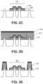
Figures 2A-2K illustrate cross-sectional views representing various operations in a method of fabricating a precision resistor for a non-planar semiconductor device architecture, in accordance with an embodiment of the present invention. Referring toFigure 2A , anisolation layer 202 is formed on apatterned bulk substrate 204 and recessed to leave a plurality offins 206 exposed. A first layer ofpolysilicon 208 and asilicon nitride hardmask 210 is then formed conformal with the plurality offins 206, as depicted inFigure 2B . Although not depicted, an insulating layer may first be formed onfins 206 to ultimately insulatepolysilicon layer 208 from the fin material. Referring toFigure 2C , a patterning process, e.g., a lithography and etch process, of the first layer ofpolysilicon 208 and thesilicon nitride hardmask 210 is performed to provide aresistor structure 212. A second layer ofpolysilicon 214 is then formed above theresistor structure 212. The second layer ofpolysilicon 214 is planarized, e.g., by a chemical mechanical polishing process, and asecond hardmask layer 216 is formed thereon, as depicted inFigure 2D . Referring toFigure 2E , a patterning process, e.g., a lithography and etch process, of the second layer ofpolysilicon 214 and thesecond hardmask 216 is performed to providedummy gate structures 218, which may includespacers 220. Thedummy gate structure 218 may then be masked bymask 222 and an implant process 224 is performed toresistor structure 212, as depicted inFigure 2F , e.g., to provide desired resistance characteristics forresistor structure 212. Referring toFigure 2G ,mask 222 is removed and an inter-layer dielectric layer 226 (e.g., silicon oxide) is formed over thedummy gate structures 218 and theresistor structure 212. Theinter-layer dielectric layer 226 is planarized to expose the polysilicon of thedummy gate structure 218, but to retainresistor structure 212 as un-exposed. The polysilicon of thedummy gate structures 218 is then removed, but theresistor structure 212 is retained, as depicted inFigure 2H . Referring to Figure 21,permanent gate electrodes 228, e.g., metal gate electrodes (with, possibly, high-k gate dielectric layers), are formed. Additional inter-layerdielectric material 250 is formed andcontact openings 230 are then formed to expose both thepermanent gate electrodes 228 and theresistor structure 212 for electrical connection, as depicted inFigure 2J . Although not shown, a silicidation process of the polysilicon of the resistor structure may be performed in the contact openings of the resistor, prior to formation of the contacts. Referring toFigure 2K ,contacts 232 are formed, e.g., by tungsten metal fill and polishing. Thepermanent gate structures 228 may be gate structures for a tri-gate device, while theresistor structure 212 may be a precision polysilicon resistor. The above approach may be referred to as a dual polysilicon deposition approach. - In a second fabrication approach,
Figures 3A-3K illustrate cross-sectional views representing various operations in another method of fabricating a precision resistor for a non-planar semiconductor device architecture, in accordance with an embodiment of the present invention. Referring toFigure 3A , anisolation layer 302 is formed on apatterned bulk substrate 304 and recessed to leave a plurality offins 306 exposed. A first layer ofpolysilicon 308 and asilicon nitride hardmask 310 is then formed conformal with the plurality offins 306, as depicted inFigure 3B . Although not depicted, an insulating layer may first be formed onfins 306 to ultimately insulatepolysilicon layer 308 from the fin material. Referring toFigure 3C , a patterning process, e.g., a lithography and etch process, of thesilicon nitride hardmask 310 is performed to provide aresistor mask 311. A second layer ofpolysilicon 314 is then formed above theresistor mask 311. The second layer ofpolysilicon 314 is planarized, e.g., by a chemical mechanical polishing process, and asecond hardmask layer 316 is formed thereon, as depicted inFigure 3D . Referring toFigure 3E , a patterning process, e.g., a lithography and etch process, of the first layer ofpolysilicon 308, the second layer ofpolysilicon 314, and thesecond hardmask 316 is performed to providedummy gate structures 318, which may includespacers 320, and to provideresistor structure 312. Thedummy gate structure 318 may then be masked bymask 322 and an implant process 324 is performed toresistor structure 312, as depicted inFigure 3F , e.g., to provide desired resistance characteristics forresistor structure 312. Referring toFigure 3G ,mask 322 is removed and an inter-layer dielectric layer 326 (e.g., silicon oxide) is formed over thedummy gate structures 318 and theresistor structure 312. The inter-layer dielectric layer 326 is planarized to expose the polysilicon of thedummy gate structure 318, but to retainresistor structure 312 as un-exposed. The polysilicon of thedummy gate structures 318 is then removed, but theresistor structure 312 is retained, as depicted inFigure 3H . Referring to Figure 31,permanent gate electrodes 328, e.g., metal gate electrodes (with, possibly, high-k gate dielectric layers), are formed. Additional inter-layerdielectric material 350 is formed andcontact openings 330 are then formed to expose both thepermanent gate electrodes 328 and theresistor structure 312 for electrical connection, as depicted inFigure 3J . Although not shown, a silicidation process of the polysilicon of the resistor structure may be performed in the contact openings of the resistor, prior to formation of the contacts. Referring toFigure 3K ,contacts 332 are formed, e.g., by tungsten metal fill and polishing. Thepermanent gate structures 328 may be gate structures for a tri-gate device, while theresistor structure 312 may be a precision polysilicon resistor. The above approach may be referred to as a buried hardmask stacked polysilicon resistor approach. - In a third fabrication approach,
Figures 4A-4L illustrate cross-sectional views representing various operations in another method of fabricating a precision resistor for a non-planar semiconductor device architecture, in accordance with an embodiment of the present invention. Referring toFigure 4A , anisolation layer 402 is formed on apatterned bulk substrate 404 and recessed to leave a plurality offins 406 exposed. A layer ofpolysilicon 408 is then formed above thefins 406, as depicted inFigure 4B . Although not depicted, an insulating layer may first be formed onfins 406 to ultimately insulatepolysilicon layer 408 from the fin material. Referring toFigure 4C , the layer ofpolysilicon 408 is planarized, e.g., by a chemical mechanical planarization process, and asilicon nitride hardmask 410 is then formed. A patterning process, e.g., a lithography and etch process, of thesilicon nitride hardmask 410 and the layer ofpolysilicon 408 is then performed to providedummy gate structures 418 and aresistor structure 412, which may includespacers 420, as depicted inFigure 4D . Referring toFigure 4E , thedummy gate structure 418 may then be masked bymask 422. The exposedresistor structure 412 is then recessed, e.g., by an etch process. The recessing 423, in one embodiment, involved removal of the hardmask as well as a portion of the polysilicon layer. Animplant process 424 is performed toresistor structure 412, as depicted inFigure 4F , e.g., to provide desired resistance characteristics forresistor structure 412. Referring toFigure 4G ,mask 422 is removed and an inter-layer dielectric layer 426 (e.g., silicon oxide) is formed over thedummy gate structures 418 and theresistor structure 412. Theinter-layer dielectric layer 426 is planarized to expose the polysilicon of thedummy gate structure 418, but to retainresistor structure 412 as un-exposed. The polysilicon of thedummy gate structures 418 is then removed, but theresistor structure 412 is retained, as depicted inFigure 4H . Referring to Figure 41,permanent gate electrodes 428, e.g., metal gate electrodes (with, possibly, high-k gate dielectric layers), are formed. Additional inter-layerdielectric material 450 is then formed, as depicted inFigure 4J . Referring to 4K,contact openings 430 are then formed to expose both thepermanent gate electrodes 428 and theresistor structure 412 for electrical connection. Although not shown, a silicidation process of the polysilicon of the resistor structure may be performed in the contact openings of the resistor, prior to formation of the contacts.Contacts 432 are then formed, e.g., by tungsten metal fill and polishing, as depicted inFigure 4L . Thepermanent gate structures 428 may be gate structures for a tri-gate device, while theresistor structure 412 may be a precision polysilicon resistor. The above approach may be referred to as a recessed polysilicon resistor approach. - In a fourth fabrication approach,
Figures 5A-5F illustrate cross-sectional views representing various operations in another method of fabricating a precision resistor for a non-planar semiconductor device architecture, in accordance with an embodiment of the present invention. Referring toFigure 5A , anisolation layer 502 is formed on apatterned bulk substrate 504 withhardmask portions 503 protruding there from. Theisolation layer 502 is recessed to leave a plurality offins 506 exposed, e.g., at a height of approximately 45 nanometers above theisolation layer 502, as depicted inFigure 5B . Referring toFigure 5C , aprotective oxide layer 507 is formed conformal with thefins 506, e.g., by chemical vapor deposition of a silicon oxide layer. A layer ofpolysilicon 508 is then formed above theprotective oxide layer 507, as depicted inFigure 5D . In one embodiment, theprotective oxide layer 507 has a thickness of approximately 2.5 nanometers and the layer ofpolysilicon 508 has a thickness of approximately 40 nanometers. Referring toFigure 5E , aphotoresist layer 560 is formed and patterned above the layer ofpolysilicon 508, leaving exposed a region of the layer ofpolysilicon 508 betweenfins 506. Animplant process 524, such as a high dose p+ implant process, is performed to provide a dopedpolysilicon region 562, as is also depicted inFigure 5E . Referring toFigure 5F , thephotoresist layer 560 is removed and the undoped portion of thepolysilicon layer 508 are removed, e.g., by a selective wet etch process such as tetramethylammonium hydroxide (TMAH). The remaining dopedpolysilicon region 562 may subsequently be used to form a precision resistor. The above approach may be referred to as a selectively implanted polysilicon resistor approach. - Regarding approaches of the type (II) above, in an embodiment, a hardmask is used to modify polish behavior during a poly opening polish to prevent a desired resistor area from being exposed (and, subsequently, removed). The protected polysilicon is then salicided and electrically connected to source/drain contacts.
- In a fifth fabrication approach,
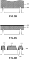
Figures 6A-6L illustrate cross-sectional views representing various operations in another method of fabricating a precision resistor for a non-planar semiconductor device architecture, in accordance with an embodiment of the present invention. Referring toFigure 6A , anisolation layer 602 is formed on apatterned bulk substrate 604 and recessed to leave a plurality offins 606 exposed. A layer ofpolysilicon 608 is then formed above thefins 606, as depicted inFigure 6B . Although not depicted, an insulating layer may first be formed onfins 606 to ultimately insulatepolysilicon layer 608 from the fin material. Referring toFigure 6C , the layer ofpolysilicon 608 is planarized, e.g., by a chemical mechanical planarization process, and asilicon nitride hardmask 610 is then formed. A patterning process, e.g., a lithography and etch process, of thesilicon nitride hardmask 610 and the layer ofpolysilicon 608 is then performed to providedummy gate structures 618 and aresistor structure 612, which may includespacers 620, as depicted inFigure 6D . Referring toFigure 6E , thedummy gate structure 618 may then be masked bymask 622. The exposedresistor structure 612 is then subjected to animplant process 624, e.g., to provide desired resistance characteristics forresistor structure 612.Mask 622 is removed and an inter-layer dielectric layer 626 (e.g., silicon oxide) is formed and planarized over thedummy gate structures 618 and theresistor structure 612, as depicted inFigure 6F . Referring toFigure 6G , asecond hardmask layer 670 is formed and patterned to coverresistor structure 612 but to exposedummy gate structures 618. The polysilicon of thedummy gate structures 618 is then removed, but theresistor structure 612 is retained, as depicted inFigure 6H . Referring to Figure 61,permanent gate electrodes 628, e.g., metal gate electrodes (with, possibly, high-k gate dielectric layers), are formed. Additional inter-layerdielectric material 650 is then formed, as depicted inFigure 6J . Referring to 6K,contact openings 630 are then formed to expose both thepermanent gate electrodes 628 and theresistor structure 612 for electrical connection.Contacts 632 are then formed, e.g., by tungsten metal fill and polishing, as depicted inFigure 6L . Although not shown, a silicidation process of the polysilicon of the resistor structure may be performed in the contact openings of the resistor, prior to formation of the contacts. Thepermanent gate structures 628 may be gate structures for a tri-gate device, while theresistor structure 612 may be a precision polysilicon resistor. - In the above described approaches, an exposed plurality of dummy gates may ultimately be replaced in a replacement gate process scheme. In such a scheme, dummy gate material such as polysilicon or silicon nitride pillar material, may be removed and replaced with permanent gate electrode material. In one such embodiment, a permanent gate dielectric layer is also formed in this process, as opposed to being carried through from earlier processing.
- In an embodiment, the plurality of dummy gates is removed by a dry etch or wet etch process. In one embodiment, the plurality of dummy gates is composed of polycrystalline silicon or amorphous silicon and is removed with a dry etch process comprising SF6. In another embodiment, the plurality of dummy gates is composed of polycrystalline silicon or amorphous silicon and is removed with a wet etch process comprising aqueous NH40H or tetramethylammonium hydroxide. In one embodiment, the plurality of dummy gates is composed of silicon nitride and is removed with a wet etch comprising aqueous phosphoric acid.
- Perhaps more generally, one or more embodiments of the present invention may be directed to a gate aligned contact process. Such a process may be implemented to form contact structures for semiconductor structure fabrication, e.g., for integrated circuit fabrication. In an embodiment, a contact pattern is formed as aligned to an existing gate pattern. By contrast, conventional approaches typically involve an additional lithography process with tight registration of a lithographic contact pattern to an existing gate pattern in combination with selective contact etches. For example, a conventional process may include patterning of a poly (gate) grid with separately patterning of contacts and contact plugs.
- Referring to
Figure 7 , aplot 700 is provided to demonstrate the variation of presently described precision resistors versus their tungsten trench counterparts, in accordance with an embodiment. Referring to plot 700, present resistors (EPR) show significantly less resistance variation the tungsten trench resistors (TCN). That is, the resistance variation is substantially reduced, enabling more accurate and tighter analog designs, for the presently described resistors. - Embodiments described herein may be applicable to designs requiring a resistor with a predictable and consistent resistance value. Current tungsten trench resistors may have large resistance and temperature variations, requiring margin to be built into a circuit. By contrast, in an embodiment, precision resistors described herein enable a simpler, smaller circuit design and footprint, along with superior matching and variability. Such characteristics may be of particular concern to analog circuit designers. The precision resistor may also be an integral collateral for system-on-chip (SoC) designers.
-
Figure 8 illustrates acomputing device 800 in accordance with one implementation of the invention. Thecomputing device 800 houses aboard 802. Theboard 802 may include a number of components, including but not limited to aprocessor 804 and at least onecommunication chip 806. Theprocessor 804 is physically and electrically coupled to theboard 802. In some implementations the at least onecommunication chip 806 is also physically and electrically coupled to theboard 802. In further implementations, thecommunication chip 806 is part of theprocessor 804. - Depending on its applications,
computing device 800 may include other components that may or may not be physically and electrically coupled to theboard 802. These other components include, but are not limited to, volatile memory (e.g., DRAM), non-volatile memory (e.g., ROM), flash memory, a graphics processor, a digital signal processor, a crypto processor, a chipset, an antenna, a display, a touchscreen display, a touchscreen controller, a battery, an audio codec, a video codec, a power amplifier, a global positioning system (GPS) device, a compass, an accelerometer, a gyroscope, a speaker, a camera, and a mass storage device (such as hard disk drive, compact disk (CD), digital versatile disk (DVD), and so forth). Thecommunication chip 806 enables wireless communications for the transfer of data to and from thecomputing device 800. The term "wireless" and its derivatives may be used to describe circuits, devices, systems, methods, techniques, communications channels, etc., that may communicate data through the use of modulated electromagnetic radiation through a non-solid medium. The term does not imply that the associated devices do not contain any wires, although in some embodiments they might not. Thecommunication chip 806 may implement any of a number of wireless standards or protocols, including but not limited to Wi-Fi (IEEE 802.11 family), WiMAX (IEEE 802.16 family), IEEE 802.20, long term evolution (LTE), Ev-DO, HSPA+, HSDPA+, HSUPA+, EDGE, GSM, GPRS, CDMA, TDMA, DECT, Bluetooth, derivatives thereof, as well as any other wireless protocols that are designated as 3G, 4G, 5G, and beyond. Thecomputing device 800 may include a plurality ofcommunication chips 806. For instance, afirst communication chip 806 may be dedicated to shorter range wireless communications such as Wi-Fi and Bluetooth and asecond communication chip 806 may be dedicated to longer range wireless communications such as GPS, EDGE, GPRS, CDMA, WiMAX, LTE, Ev-DO, and others. - The
processor 804 of thecomputing device 800 includes an integrated circuit die packaged within theprocessor 804. In some implementations of the invention, the integrated circuit die of the processor includes one or more devices, such as MOS-FET transistors built in accordance with implementations of the invention. The term "processor" may refer to any device or portion of a device that processes electronic data from registers and/or memory to transform that electronic data into other electronic data that may be stored in registers and/or memory. - The
communication chip 806 also includes an integrated circuit die packaged within thecommunication chip 806. In accordance with another implementation of the invention, the integrated circuit die of the communication chip includes one or more devices, such as precision resistors for non-planar semiconductor device architectures built in accordance with implementations of the invention. - In further implementations, another component housed within the
computing device 800 may contain an integrated circuit die that includes one or more devices, such as precision resistors for non-planar semiconductor device architectures built in accordance with implementations of the invention. - In various implementations, the
computing device 800 may be a laptop, a netbook, a notebook, an ultrabook, a smartphone, a tablet, a personal digital assistant (PDA), an ultra mobile PC, a mobile phone, a desktop computer, a server, a printer, a scanner, a monitor, a set-top box, an entertainment control unit, a digital camera, a portable music player, or a digital video recorder. In further implementations, thecomputing device 800 may be any other electronic device that processes data. - Thus, embodiments of the present invention include precision resistors for non-planar semiconductor device architectures and methods of fabricating precision resistors for non-planar semiconductor device architectures.
- In an embodiment, a semiconductor structure includes first and second semiconductor fins disposed above a substrate. A resistor structure is disposed above the first semiconductor fin but not above the second semiconductor fin. A transistor structure is formed from the second semiconductor fin but not from the first semiconductor fin.
- In one embodiment, the resistor structure includes a resistive material layer disposed conformal with the first semiconductor fin.
- In one embodiment, the resistive material layer is composed of polycrystalline silicon.
- In one embodiment, the polycrystalline silicon has a grain size of approximately 20 nanometers.
- In one embodiment, the polycrystalline silicon is doped with boron with a dose approximately in the range of lE15 - lE17 atoms/cm2.
- In one embodiment, the resistive material layer has a resistance that is essentially independent of temperature over a working temperature range of the resistor structure.
- In one embodiment, the semiconductor structure further includes an electrically insulating layer disposed between the resistive material layer and the first semiconductor fin.
- In one embodiment, the resistor structure includes tungsten metal contacts coupled to nickel silicide regions disposed in the polycrystalline silicon.
- In one embodiment, the transistor structure includes source and drain regions disposed in the second semiconductor fin, and a gate stack disposed above the second semiconductor fin, and the gate stack includes a high-k gate dielectric layer and a metal gate electrode.
- In one embodiment, the first semiconductor fin is of a first plurality of semiconductor fins and the second semiconductor fin is of a second plurality of semiconductor fins, the resistor structure is disposed above the first plurality of semiconductor fins but not above the second plurality of semiconductor fins, and the transistor structure is formed from the second plurality of semiconductor fins but not from the first plurality of semiconductor fins.
- In one embodiment, the first and second pluralities of semiconductor fins are electrically coupled to an underlying bulk semiconductor substrate.
- In one embodiment, the resistor structure is a non-planar resistor structure.
- In another embodiment, a semiconductor structure includes first and second semiconductor fins disposed above a substrate. An isolation region is disposed above the substrate, between the first and second semiconductor fins, and at a height less than the first and second semiconductor fins. A resistor structure is disposed above the isolation region but not above the first and second semiconductor fins. First and second transistor structures are formed from the first and second semiconductor fins, respectively.
- In one embodiment, the resistor structure includes a resistive material layer disposed conformal with the isolation region.
- In one embodiment, the resistive material layer is composed of polycrystalline silicon.
- In one embodiment, the polycrystalline silicon has a grain size of approximately 20 nanometers.
- In one embodiment, the polycrystalline silicon is doped with boron with a dose approximately in the range of 1E15 - 1E17 atoms/cm2.
- In one embodiment, the resistive material layer has a resistance that is essentially independent of temperature over a working temperature range of the resistor structure.
- In one embodiment, the resistive material layer has a top surface at a height less than the heights of the first and second semiconductor fins.
- In one embodiment, the resistor structure includes tungsten metal contacts coupled to nickel silicide regions disposed in the polycrystalline silicon.
- In one embodiment, the first and second transistor structures each includes source and drain regions disposed in the first or second semiconductor fin, respectively, and a gate stack disposed above the first and second semiconductor fin, respectively. Each gate stack includes a high-k gate dielectric layer and a metal gate electrode.
- In one embodiment, the first semiconductor fin is of a first plurality of semiconductor fins and the second semiconductor fin is of a second plurality of semiconductor fins, and the first transistor structure is formed from the first plurality of semiconductor fins and the second transistor structure is formed from the second plurality of semiconductor fins.
- In one embodiment, the first and second pluralities of semiconductor fins are electrically coupled to an underlying bulk semiconductor substrate.
- In one embodiment, the resistor structure is a planar resistor structure.
- In an embodiment, a method of fabricating a semiconductor structure includes forming first and second semiconductor fins above a substrate. The method also includes forming a resistor structure above the first semiconductor fin but not above the second semiconductor fin. The method also includes forming a transistor structure from the second semiconductor fin but not from the first semiconductor fin. Forming the transistor structure includes forming one or more dummy gates above the second semiconductor fin and, subsequent to forming the resistor structure, replacing the one or more dummy gates with a permanent gate stack.
- In one embodiment, forming the resistor structure includes forming a resistive material layer conformal with the first semiconductor fin.
- In one embodiment, forming the resistive material layer includes forming a polycrystalline silicon layer having a grain size of approximately 20 nanometers.
- In an embodiment, a method of fabricating a semiconductor structure includes forming first and second semiconductor fins above a substrate. The method also includes forming an isolation region above the substrate, between the first and second semiconductor fins, and at a height less than the first and second semiconductor fins. The method also includes forming a resistor structure above the isolation region but not above the first and second semiconductor fins. The method also includes forming first and second transistor structures from the first and second semiconductor fins, respectively. Forming the first and second transistor structures includes forming one or more dummy gates above the first and second semiconductor fins and, subsequent to forming the resistor structure, replacing the one or more dummy gates with a permanent gate stack.
- In one embodiment, forming the resistor structure includes forming a resistive material layer conformal with the isolation region.
- In one embodiment, forming the resistive material layer includes forming a polycrystalline silicon layer having a grain size of approximately 20 nanometers.
- Embodiments of the invention also include the following aspects:
- 1. A device, comprising:
- a first fin including silicon;
- a second fin including silicon;
- an insulating material having a region between the first fin and the second fin, wherein the insulating material includes silicon and oxygen;
- a resistor above the region of the insulating material, wherein the resistor includes polycrystalline silicon;
- conductive contact coupled to a location at a top surface of the resistor, wherein the resistor is at least partially between the conductive contact and the insulating material, and the conductive contact includes tungsten;
- a first metal region at least partially above the first fin, wherein the first metal region extends down proximate to side faces of the first fin, and the first metal region includes a transition metal;
- a first dielectric region at least partially between the first fin and the first metal region, wherein the first dielectric region includes hafnium;
- a second metal region at least partially above the second fin, wherein the second metal region extends down proximate to side faces of the second fin, and the second metal region includes a transition metal; and
- a second dielectric region at least partially between the second fin and the second metal region, wherein the second dielectric region includes hafnium;
- wherein the location at the top surface of the resistor has a first height, a top surface of the first metal region has a second height, a top surface of the second metal region has a third height, the first height is less than the second height, and the first height is less than the third height.
- 2. The device of aspect 1, wherein the first metal region includes a transition metal nitride or a transition metal aluminide, and the second metal region includes a transition metal nitride or a transition metal aluminide.
- 3. The device of aspect 1, wherein the first dielectric region includes hafnium oxide, the second dielectric region includes hafnium oxide, the first dielectric region includes silicon oxide between the hafnium oxide and the first fin, and the second dielectric region includes silicon oxide between the hafnium oxide and the second fin.
- 4. The device of aspect 1, wherein the resistor includes boron.
- 5. The device of aspect 1, wherein the conductive contact includes silicon between the tungsten and the resistor.
- 6. The device of aspect 1, further comprising:
dielectric material above the resistor, wherein the dielectric material has a top surface that is co-planar with the top surface of the first metal region and co-planar with the top surface of the second metal region, wherein the conductive contact extends through the dielectric material. - 7. The device of aspect 6, wherein the dielectric material includes silicon oxide.
- 8. The device of any of claims 1-6, further comprising:
a substrate comprising silicon, wherein the insulating material is at least partially between the substrate and the resistor. - 9. The device of any of aspects 1-6, wherein the first metal region, the first dielectric region, and a portion of the first fin are part of a first transistor, and wherein the second metal region, the second dielectric region, and a portion of the second fin are part of a second transistor.
- 10. The device of any of aspects 1-6, wherein a longitudinal axis of the first fin is perpendicular to a longitudinal axis of the resistor, and a longitudinal axis of the second fin is perpendicular to the longitudinal axis of the resistor.
- 11. The device of any of aspects 1-6, wherein the region of the insulating material has a top surface with at least a portion of the top surface in a plane below the resistor, the first height is measured from the plane, the second height is measured from the plane, and the third height is measured from the plane.
- 12. An integrated circuit (IC) die, comprising:
- a first fin including silicon;
- a second fin including silicon;
- an insulating material having a region between the first fin and the second fin, wherein the STI material includes silicon and oxygen;
- a resistor above the region of the insulating material, wherein the resistor includes polycrystalline silicon;
- a conductive contact coupled to a location at a top surface of the resistor, wherein the resistor is at least partially between the conductive contact and the insulating material, and the conductive contact includes tungsten;
- a first metal region at least partially above the first fin, wherein the first metal region extends down proximate to side faces of the first fin, and the first metal region includes a transition metal;
- a first dielectric region at least partially between the first fin and the first metal region, wherein the first dielectric region includes hafnium;
- a second metal region at least partially above the second fin, wherein the second metal region extends down proximate to side faces of the second fin, and the second metal region includes a transition metal; and
- a second dielectric region at least partially between the second fin and the second metal region, wherein the second dielectric region includes hafnium;
- wherein the location at the top surface of the resistor has a first height, a top surface of the first metal region has a second height, a top surface of the second metal region has a third height, the first height is less than the second height, and the first height is less than the third height.
- 13. The IC die of aspect 12, wherein:
- the first metal region, the first dielectric region, and a portion of the first fin are part of a first transistor;
- the second metal region, the second dielectric region, and a portion of the second fin are part of a second transistor; and
- the first transistor and the second transistor are included in a processing device.
- 14. A method of manufacturing a device, comprising:
- forming a first fin including silicon;
- forming a second fin including silicon;
- providing an insulating material having a region between the first fin and the second fin, wherein the insulating material includes silicon and oxygen;
- forming a resistor above the region of the STI material, wherein the resistor includes polycrystalline silicon;
- forming a conductive contact coupled to a location at a top surface of the resistor, wherein the resistor is at least partially between the conductive contact and the STI material, and the conductive contact includes tungsten;
- providing a first dielectric region at least partially above the first fin, wherein the first dielectric region includes hafnium;
- providing a first metal region at least partially above the first dielectric region, wherein the first metal region extends down proximate to portions of side faces of the first fin, and the first metal region includes a transition metal;
- providing a second dielectric region at least partially above the second fin, wherein the second dielectric region includes hafnium
- providing a second metal region at least partially above the second dielectric region, wherein the second metal region extends down proximate to side faces of the second fin, and the second metal region includes a transition metal; and
- wherein the location at the top surface of the resistor has a first height, a top surface of the first metal region has a second height, a top surface of the second metal region has a third height, the first height is less than the second height, and the first height is less than the third height.
- 15. The method of aspect 14, further comprising:
- providing a first dummy gate stack on the first fin;
- providing a second dummy gate stack on the second fin;
- providing insulating material around the first dummy gate stack and the second dummy gate stack;
- removing the first dummy gate stack to form a first recess in the insulating material;
- removing the second dummy gate stack to form a second recess in the insulating material;
- providing a first replacement gate stack in the first recess; and
- providing a second replacement gate stack in the second recess.
Claims (7)
- A semiconductor device, comprising:a first fin and a second fin, wherein the first fin and the second fin include silicon;an isolation region between lower parts of the first fin and the second fin;a resistor above the top surface of the isolation region but not above the first fin and not above the second fin, wherein the resistor is a planar resistor;conductive contacts coupled to the resistor;a first transistor including a portion of the first fin, wherein the first transistor includes a first gate electrode above the first fin, the first gate electrode includes a first material and a second material different from the first material, the first material is between the second material and the first fin, the second material includes tungsten, the first material or the second material includes titanium, the first transistor includes silicon oxide between the first gate electrode and the first fin, and the first transistor includes hafnium oxide between the silicon oxide and the first gate electrode; anda second transistor including a portion of the second fin, wherein the second transistor includes a second gate electrode above the second fin, the second gate electrode includes the first material and the second material, the first material is between the second material and the second fin, the second transistor includes silicon oxide between the second gate electrode and the second fin, and the second transistor includes hafnium oxide between the silicon oxide and the second gate electrode.
- The device of claim 1, wherein the resistor has a top surface with a height, at a location between the first fin and the second fin, greater than a height of the first fin and greater than a height of the second fin.
- The device of any one of claims 1-2, wherein the conductive contacts extend into openings in the resistor.
- The device of claim 3, wherein the conductive contacts have a tapered shape.
- The device of any one of claims 1-4, wherein the first material is a workfunction-setting layer.
- The device of any one of claims 1-5, wherein the first fin and the second fin include undoped silicon.
- The device of any one of claims 1-6, wherein the first fin and the second fin are part of a patterned substrate.
Applications Claiming Priority (4)
| Application Number | Priority Date | Filing Date | Title |
|---|---|---|---|
| US13/625,698 US8796772B2 (en) | 2012-09-24 | 2012-09-24 | Precision resistor for non-planar semiconductor device architecture |
| EP17191534.1A EP3285300A1 (en) | 2012-09-24 | 2013-06-18 | Precision resistor for non-planar semiconductor device architecture |
| PCT/US2013/046395 WO2014046755A1 (en) | 2012-09-24 | 2013-06-18 | Precision resistor for non-planar semiconductor device architecture |
| EP13839477.0A EP2898533B1 (en) | 2012-09-24 | 2013-06-18 | Precision resistor for non-planar semiconductor device architecture |
Related Parent Applications (3)
| Application Number | Title | Priority Date | Filing Date |
|---|---|---|---|
| EP13839477.0A Division EP2898533B1 (en) | 2012-09-24 | 2013-06-18 | Precision resistor for non-planar semiconductor device architecture |
| EP13839477.0A Division-Into EP2898533B1 (en) | 2012-09-24 | 2013-06-18 | Precision resistor for non-planar semiconductor device architecture |
| EP17191534.1A Division EP3285300A1 (en) | 2012-09-24 | 2013-06-18 | Precision resistor for non-planar semiconductor device architecture |
Publications (2)
| Publication Number | Publication Date |
|---|---|
| EP4283676A2 true EP4283676A2 (en) | 2023-11-29 |
| EP4283676A3 EP4283676A3 (en) | 2024-07-17 |
Family
ID=50338031
Family Applications (4)
| Application Number | Title | Priority Date | Filing Date |
|---|---|---|---|
| EP13839477.0A Active EP2898533B1 (en) | 2012-09-24 | 2013-06-18 | Precision resistor for non-planar semiconductor device architecture |
| EP17152588.4A Pending EP3182452A1 (en) | 2012-09-24 | 2013-06-18 | Precision resistor for non-planar semiconductor device architecture |
| EP23193624.6A Pending EP4283676A3 (en) | 2012-09-24 | 2013-06-18 | Precision resistor for non-planar semiconductor device architecture |
| EP17191534.1A Pending EP3285300A1 (en) | 2012-09-24 | 2013-06-18 | Precision resistor for non-planar semiconductor device architecture |
Family Applications Before (2)
| Application Number | Title | Priority Date | Filing Date |
|---|---|---|---|
| EP13839477.0A Active EP2898533B1 (en) | 2012-09-24 | 2013-06-18 | Precision resistor for non-planar semiconductor device architecture |
| EP17152588.4A Pending EP3182452A1 (en) | 2012-09-24 | 2013-06-18 | Precision resistor for non-planar semiconductor device architecture |
Family Applications After (1)
| Application Number | Title | Priority Date | Filing Date |
|---|---|---|---|
| EP17191534.1A Pending EP3285300A1 (en) | 2012-09-24 | 2013-06-18 | Precision resistor for non-planar semiconductor device architecture |
Country Status (6)
| Country | Link |
|---|---|
| US (2) | US8796772B2 (en) |
| EP (4) | EP2898533B1 (en) |
| KR (3) | KR101969243B1 (en) |
| CN (4) | CN110400801B (en) |
| TW (4) | TWI487116B (en) |
| WO (1) | WO2014046755A1 (en) |
Families Citing this family (33)
| Publication number | Priority date | Publication date | Assignee | Title |
|---|---|---|---|---|
| US8962421B2 (en) * | 2012-11-15 | 2015-02-24 | GlobalFoundries, Inc. | Methods for fabricating integrated circuits including semiconductive resistor structures in a FinFET architecture |
| US9196542B2 (en) * | 2013-05-22 | 2015-11-24 | United Microelectronics Corp. | Method for manufacturing semiconductor devices |
| US9941271B2 (en) * | 2013-10-04 | 2018-04-10 | Avago Technologies General Ip (Singapore) Pte. Ltd. | Fin-shaped field effect transistor and capacitor structures |
| US9490176B2 (en) * | 2014-10-17 | 2016-11-08 | Taiwan Semiconductor Manufacturing Company, Ltd. | Method and structure for FinFET isolation |
| US9685434B2 (en) | 2014-12-10 | 2017-06-20 | International Business Machines Corporation | Inter-level dielectric layer in replacement metal gates and resistor fabrication |
| TWI620358B (en) * | 2015-01-28 | 2018-04-01 | 旺宏電子股份有限公司 | Memory structure and manufacturing method of the same |
| US9514998B1 (en) | 2015-05-11 | 2016-12-06 | International Business Machines Corporation | Polysilicon resistor formation in silicon-on-insulator replacement metal gate finFET processes |
| CN107924948B (en) * | 2015-08-26 | 2023-12-05 | 英特尔公司 | Composite lateral resistor structure for integrated circuits |
| US10050030B2 (en) * | 2015-09-04 | 2018-08-14 | Taiwan Semiconductor Manufacturing Company, Ltd. | Semiconductor device and fabricating method thereof |
| CN107924945B (en) * | 2015-09-25 | 2021-10-01 | 英特尔公司 | Power door with metal on both sides |
| US9570571B1 (en) | 2015-11-18 | 2017-02-14 | International Business Machines Corporation | Gate stack integrated metal resistors |
| US10903372B2 (en) * | 2015-12-11 | 2021-01-26 | Intel Corporation | Metal-oxide-polysilicon tunable resistor for flexible circuit design and method of fabricating same |
| WO2017111771A1 (en) * | 2015-12-23 | 2017-06-29 | Intel Corporation | Thin film polysilicon resistor by gate-to-gate isolation |
| CN106935504B (en) * | 2015-12-30 | 2019-11-01 | 中芯国际集成电路制造(上海)有限公司 | Semiconductor structure and forming method thereof |
| WO2018004672A1 (en) * | 2016-07-01 | 2018-01-04 | Intel Corporation | Thin film resistor with reduced capacitance |
| CN107677386B (en) * | 2016-08-02 | 2019-07-26 | 中芯国际集成电路制造(上海)有限公司 | Semiconductor structure and thermometry for temperature measurement |
| US10002868B2 (en) | 2016-09-30 | 2018-06-19 | International Business Machines Corporation | Vertical fin resistor devices |
| US10930729B2 (en) | 2016-10-21 | 2021-02-23 | Intel Corporation | Fin-based thin film resistor |
| US9997590B2 (en) | 2016-10-24 | 2018-06-12 | International Büsiness Machines Corporation | FinFET resistor and method to fabricate same |
| US9954050B1 (en) | 2016-10-24 | 2018-04-24 | International Business Machines Corporation | Precise/designable FinFET resistor structure |
| US10872889B2 (en) * | 2016-11-17 | 2020-12-22 | Taiwan Semiconductor Manufacturing Co., Ltd. | Semiconductor component and fabricating method thereof |
| US10411085B2 (en) | 2016-12-29 | 2019-09-10 | Taiwan Semiconductor Manufacturing Co., Ltd. | Semiconductor device and a method for fabricating the same |
| US10840354B2 (en) * | 2017-02-06 | 2020-11-17 | International Business Machines Corporation | Approach to bottom dielectric isolation for vertical transport fin field effect transistors |
| US10056469B1 (en) * | 2017-02-13 | 2018-08-21 | Globalfoundries Inc. | Gate cut integration and related device |
| US10074575B1 (en) | 2017-06-21 | 2018-09-11 | International Business Machines Corporation | Integrating and isolating nFET and pFET nanosheet transistors on a substrate |
| US10770302B2 (en) * | 2018-09-27 | 2020-09-08 | Taiwan Semiconductor Manufacturing Company, Ltd. | Semiconductor FinFET device and method |
| US11056537B2 (en) | 2019-03-27 | 2021-07-06 | International Business Machines Corporation | Self-aligned gate contact integration with metal resistor |
| TW202119438A (en) * | 2019-10-31 | 2021-05-16 | 日商索尼半導體解決方案公司 | Resistance element and electronic device |
| US11233117B2 (en) | 2019-10-31 | 2022-01-25 | Taiwan Semiconductor Manufacturing Company, Ltd. | Ring structure for film resistor |
| KR20210064593A (en) | 2019-11-26 | 2021-06-03 | 삼성전자주식회사 | Semiconductor devices |
| KR20210072477A (en) | 2019-12-09 | 2021-06-17 | 삼성전자주식회사 | Resistor with doped regions |
| US20220238516A1 (en) * | 2021-01-25 | 2022-07-28 | Yanbiao Pan | Polysilicon resistor using reduced grain size polysilicon |
| CN116799004B (en) * | 2023-08-23 | 2023-11-28 | 合肥晶合集成电路股份有限公司 | Semiconductor integrated device and manufacturing method thereof |
Family Cites Families (36)
| Publication number | Priority date | Publication date | Assignee | Title |
|---|---|---|---|---|
| US4467519A (en) | 1982-04-01 | 1984-08-28 | International Business Machines Corporation | Process for fabricating polycrystalline silicon film resistors |
| TW478050B (en) * | 2001-03-21 | 2002-03-01 | Taiwan Semiconductor Mfg | Method of fabricating polysilicon resistor on metal gate |
| US6803680B2 (en) * | 2002-09-13 | 2004-10-12 | Mia-Com, Inc. | Apparatus, methods, and articles of manufacture for a switch having sharpened control voltage |
| US7173305B2 (en) * | 2003-04-08 | 2007-02-06 | Taiwan Semiconductor Manufacturing Company, Ltd. | Self-aligned contact for silicon-on-insulator devices |
| KR100618827B1 (en) * | 2004-05-17 | 2006-09-08 | 삼성전자주식회사 | Semiconductor device comprising FinFET and fabricating method thereof |
| US7397087B2 (en) * | 2004-08-06 | 2008-07-08 | International Business Machines Corporation | FEOL/MEOL metal resistor for high end CMOS |
| US7227183B2 (en) * | 2004-09-17 | 2007-06-05 | International Business Machines Corporation | Polysilicon conductor width measurement for 3-dimensional FETs |
| TWI267951B (en) * | 2004-09-30 | 2006-12-01 | Taiwan Semiconductor Mfg | A device having multiple silicide types and a method for its fabrication |
| US20070018239A1 (en) * | 2005-07-20 | 2007-01-25 | International Business Machines Corporation | Sea-of-fins structure on a semiconductor substrate and method of fabrication |
| US7479421B2 (en) * | 2005-09-28 | 2009-01-20 | Intel Corporation | Process for integrating planar and non-planar CMOS transistors on a bulk substrate and article made thereby |
| US8174073B2 (en) * | 2007-05-30 | 2012-05-08 | Taiwan Semiconductor Manufacturing Co., Ltd. | Integrated circuit structures with multiple FinFETs |
| US7994020B2 (en) * | 2008-07-21 | 2011-08-09 | Advanced Micro Devices, Inc. | Method of forming finned semiconductor devices with trench isolation |
| US7879666B2 (en) * | 2008-07-23 | 2011-02-01 | Freescale Semiconductor, Inc. | Semiconductor resistor formed in metal gate stack |
| US20100059823A1 (en) * | 2008-09-10 | 2010-03-11 | Taiwan Semiconductor Manufacturing Company, Ltd. | Resistive device for high-k metal gate technology and method of making |
| US8138037B2 (en) * | 2009-03-17 | 2012-03-20 | International Business Machines Corporation | Method and structure for gate height scaling with high-k/metal gate technology |
| US7955928B2 (en) * | 2009-03-30 | 2011-06-07 | International Business Machines Corporation | Structure and method of fabricating FinFET |
| US7960282B2 (en) * | 2009-05-21 | 2011-06-14 | Globalfoundries Singapore Pte. Ltd. | Method of manufacture an integrated circuit system with through silicon via |
| US8053809B2 (en) * | 2009-05-26 | 2011-11-08 | International Business Machines Corporation | Device including high-K metal gate finfet and resistive structure and method of forming thereof |
| US8193900B2 (en) * | 2009-06-24 | 2012-06-05 | United Microelectronics Corp. | Method for fabricating metal gate and polysilicon resistor and related polysilicon resistor structure |
| US8980719B2 (en) * | 2010-04-28 | 2015-03-17 | Taiwan Semiconductor Manufacturing Company, Ltd. | Methods for doping fin field-effect transistors |
| US8890260B2 (en) * | 2009-09-04 | 2014-11-18 | Taiwan Semiconductor Manufacturing Company, Ltd. | Polysilicon design for replacement gate technology |
| US7985639B2 (en) * | 2009-09-18 | 2011-07-26 | GlobalFoundries, Inc. | Method for fabricating a semiconductor device having a semiconductive resistor structure |
| US7993999B2 (en) * | 2009-11-09 | 2011-08-09 | International Business Machines Corporation | High-K/metal gate CMOS finFET with improved pFET threshold voltage |
| US20110147831A1 (en) * | 2009-12-23 | 2011-06-23 | Steigerwald Joseph M | Method for replacement metal gate fill |
| US8389359B2 (en) * | 2010-02-08 | 2013-03-05 | Taiwan Semiconductor Manufacturing Company, Ltd. | Method for forming low resistance and uniform metal gate |
| JP2011181841A (en) * | 2010-03-03 | 2011-09-15 | Toshiba Corp | Method of manufacturing semiconductor device |
| US8546228B2 (en) * | 2010-06-16 | 2013-10-01 | International Business Machines Corporation | Strained thin body CMOS device having vertically raised source/drain stressors with single spacer |
| US8278173B2 (en) * | 2010-06-30 | 2012-10-02 | Taiwan Semiconductor Manufacturing Company, Ltd. | Method of fabricating gate structures |
| US8058125B1 (en) * | 2010-08-04 | 2011-11-15 | Taiwan Semiconductor Manufacturing Company, Ltd. | Poly resistor on a semiconductor device |
| US9385050B2 (en) * | 2011-01-06 | 2016-07-05 | Globalfoundries Inc. | Structure and method to fabricate resistor on finFET processes |
| US9269758B2 (en) * | 2011-01-13 | 2016-02-23 | Taiwan Semiconductor Manufacturing Company, Ltd. | Low TCR high resistance resistor |
| US9293584B2 (en) * | 2011-11-02 | 2016-03-22 | Broadcom Corporation | FinFET devices |
| US9087687B2 (en) * | 2011-12-23 | 2015-07-21 | International Business Machines Corporation | Thin heterostructure channel device |
| US8569127B2 (en) * | 2012-03-13 | 2013-10-29 | United Microelectronics Corp. | Semiconductor device and method for fabricating the same |
| US8816436B2 (en) * | 2012-05-16 | 2014-08-26 | International Business Machines Corporation | Method and structure for forming fin resistors |
| US9093556B2 (en) * | 2012-08-21 | 2015-07-28 | Stmicroelectronics, Inc. | Multi-fin FINFET device including epitaxial growth barrier on outside surfaces of outermost fins and related methods |
-
2012
- 2012-09-24 US US13/625,698 patent/US8796772B2/en active Active
-
2013
- 2013-06-18 WO PCT/US2013/046395 patent/WO2014046755A1/en unknown
- 2013-06-18 CN CN201910635550.3A patent/CN110400801B/en active Active
- 2013-06-18 CN CN201380042912.9A patent/CN104541377B/en active Active
- 2013-06-18 KR KR1020177003659A patent/KR101969243B1/en active IP Right Grant
- 2013-06-18 EP EP13839477.0A patent/EP2898533B1/en active Active
- 2013-06-18 EP EP17152588.4A patent/EP3182452A1/en active Pending
- 2013-06-18 EP EP23193624.6A patent/EP4283676A3/en active Pending
- 2013-06-18 CN CN201710228504.2A patent/CN107256858B/en active Active
- 2013-06-18 EP EP17191534.1A patent/EP3285300A1/en active Pending
- 2013-06-18 KR KR1020177009819A patent/KR101969246B1/en active IP Right Grant
- 2013-06-18 CN CN201710067644.6A patent/CN106971978B/en active Active
- 2013-06-18 KR KR1020157001592A patent/KR101707754B1/en active IP Right Grant
- 2013-09-04 TW TW102131802A patent/TWI487116B/en active
- 2013-09-04 TW TW104108118A patent/TWI552311B/en active
- 2013-09-04 TW TW106110332A patent/TWI623082B/en active
- 2013-09-04 TW TW105123243A patent/TWI610419B/en active
-
2014
- 2014-06-24 US US14/313,678 patent/US8889508B2/en active Active
Also Published As
| Publication number | Publication date |
|---|---|
| TWI487116B (en) | 2015-06-01 |
| TW201709480A (en) | 2017-03-01 |
| EP4283676A3 (en) | 2024-07-17 |
| CN104541377B (en) | 2019-08-20 |
| CN107256858B (en) | 2020-11-10 |
| KR20170018478A (en) | 2017-02-17 |
| TW201727871A (en) | 2017-08-01 |
| EP3285300A1 (en) | 2018-02-21 |
| TWI610419B (en) | 2018-01-01 |
| TW201539712A (en) | 2015-10-16 |
| US20140308785A1 (en) | 2014-10-16 |
| KR101969243B1 (en) | 2019-04-15 |
| CN110400801B (en) | 2024-03-01 |
| TWI623082B (en) | 2018-05-01 |
| EP3182452A1 (en) | 2017-06-21 |
| KR20170042826A (en) | 2017-04-19 |
| WO2014046755A1 (en) | 2014-03-27 |
| EP2898533B1 (en) | 2024-07-10 |
| US8889508B2 (en) | 2014-11-18 |
| KR20150034188A (en) | 2015-04-02 |
| EP2898533A1 (en) | 2015-07-29 |
| CN107256858A (en) | 2017-10-17 |
| CN104541377A (en) | 2015-04-22 |
| US8796772B2 (en) | 2014-08-05 |
| KR101969246B1 (en) | 2019-04-15 |
| EP2898533A4 (en) | 2016-08-31 |
| CN110400801A (en) | 2019-11-01 |
| CN106971978A (en) | 2017-07-21 |
| TWI552311B (en) | 2016-10-01 |
| KR101707754B1 (en) | 2017-02-16 |
| US20140084381A1 (en) | 2014-03-27 |
| TW201432908A (en) | 2014-08-16 |
| CN106971978B (en) | 2021-03-12 |
Similar Documents
| Publication | Publication Date | Title |
|---|---|---|
| US8889508B2 (en) | Precision resistor for non-planar semiconductor device architecture | |
| US12015087B2 (en) | Semiconductor device having a necked semiconductor body and method of forming semiconductor bodies of varying width | |
| US10263112B2 (en) | Vertical non-planar semiconductor device for system-on-chip (SoC) applications | |
| EP3425675B1 (en) | Non-planar semiconductor device having omega-fin with doped sub-fin region | |
| CN106847924B (en) | Non-planar semiconductor device with doped sub-fin regions and method of fabricating the same | |
| US9881927B2 (en) | CMOS-compatible polycide fuse structure and method of fabricating same | |
| US10892192B2 (en) | Non-planar I/O and logic semiconductor devices having different workfunction on common substrate |
Legal Events
| Date | Code | Title | Description |
|---|---|---|---|
| PUAI | Public reference made under article 153(3) epc to a published international application that has entered the european phase |
Free format text: ORIGINAL CODE: 0009012 |
|
| STAA | Information on the status of an ep patent application or granted ep patent |
Free format text: STATUS: REQUEST FOR EXAMINATION WAS MADE |
|
| 17P | Request for examination filed |
Effective date: 20230828 |
|
| AC | Divisional application: reference to earlier application |
Ref document number: 2898533 Country of ref document: EP Kind code of ref document: P Ref document number: 3285300 Country of ref document: EP Kind code of ref document: P |
|
| AK | Designated contracting states |
Kind code of ref document: A2 Designated state(s): AL AT BE BG CH CY CZ DE DK EE ES FI FR GB GR HR HU IE IS IT LI LT LU LV MC MK MT NL NO PL PT RO RS SE SI SK SM TR |
|
| PUAL | Search report despatched |
Free format text: ORIGINAL CODE: 0009013 |
|
| AK | Designated contracting states |
Kind code of ref document: A3 Designated state(s): AL AT BE BG CH CY CZ DE DK EE ES FI FR GB GR HR HU IE IS IT LI LT LU LV MC MK MT NL NO PL PT RO RS SE SI SK SM TR |
|
| RIC1 | Information provided on ipc code assigned before grant |
Ipc: H01L 21/8234 20060101ALN20240607BHEP Ipc: H01L 29/66 20060101ALN20240607BHEP Ipc: H01L 27/088 20060101ALN20240607BHEP Ipc: H10N 97/00 20230101ALI20240607BHEP Ipc: H01L 27/06 20060101AFI20240607BHEP |