EP4270933A1 - Bildgebungselement und bildgebungsvorrichtung - Google Patents
Bildgebungselement und bildgebungsvorrichtung Download PDFInfo
- Publication number
- EP4270933A1 EP4270933A1 EP21915115.6A EP21915115A EP4270933A1 EP 4270933 A1 EP4270933 A1 EP 4270933A1 EP 21915115 A EP21915115 A EP 21915115A EP 4270933 A1 EP4270933 A1 EP 4270933A1
- Authority
- EP
- European Patent Office
- Prior art keywords
- unit
- charge
- wiring
- charge retaining
- retaining unit
- Prior art date
- Legal status (The legal status is an assumption and is not a legal conclusion. Google has not performed a legal analysis and makes no representation as to the accuracy of the status listed.)
- Pending
Links
Images







Classifications
-
- H—ELECTRICITY
- H10—SEMICONDUCTOR DEVICES; ELECTRIC SOLID-STATE DEVICES NOT OTHERWISE PROVIDED FOR
- H10F—INORGANIC SEMICONDUCTOR DEVICES SENSITIVE TO INFRARED RADIATION, LIGHT, ELECTROMAGNETIC RADIATION OF SHORTER WAVELENGTH OR CORPUSCULAR RADIATION
- H10F39/00—Integrated devices, or assemblies of multiple devices, comprising at least one element covered by group H10F30/00, e.g. radiation detectors comprising photodiode arrays
- H10F39/80—Constructional details of image sensors
- H10F39/803—Pixels having integrated switching, control, storage or amplification elements
- H10F39/8037—Pixels having integrated switching, control, storage or amplification elements the integrated elements comprising a transistor
-
- H—ELECTRICITY
- H04—ELECTRIC COMMUNICATION TECHNIQUE
- H04N—PICTORIAL COMMUNICATION, e.g. TELEVISION
- H04N25/00—Circuitry of solid-state image sensors [SSIS]; Control thereof
- H04N25/50—Control of the SSIS exposure
- H04N25/57—Control of the dynamic range
- H04N25/59—Control of the dynamic range by controlling the amount of charge storable in the pixel, e.g. modification of the charge conversion ratio of the floating node capacitance
-
- H—ELECTRICITY
- H04—ELECTRIC COMMUNICATION TECHNIQUE
- H04N—PICTORIAL COMMUNICATION, e.g. TELEVISION
- H04N25/00—Circuitry of solid-state image sensors [SSIS]; Control thereof
- H04N25/70—SSIS architectures; Circuits associated therewith
- H04N25/76—Addressed sensors, e.g. MOS or CMOS sensors
- H04N25/77—Pixel circuitry, e.g. memories, A/D converters, pixel amplifiers, shared circuits or shared components
-
- H—ELECTRICITY
- H04—ELECTRIC COMMUNICATION TECHNIQUE
- H04N—PICTORIAL COMMUNICATION, e.g. TELEVISION
- H04N25/00—Circuitry of solid-state image sensors [SSIS]; Control thereof
- H04N25/70—SSIS architectures; Circuits associated therewith
- H04N25/76—Addressed sensors, e.g. MOS or CMOS sensors
- H04N25/77—Pixel circuitry, e.g. memories, A/D converters, pixel amplifiers, shared circuits or shared components
- H04N25/771—Pixel circuitry, e.g. memories, A/D converters, pixel amplifiers, shared circuits or shared components comprising storage means other than floating diffusion
-
- H—ELECTRICITY
- H10—SEMICONDUCTOR DEVICES; ELECTRIC SOLID-STATE DEVICES NOT OTHERWISE PROVIDED FOR
- H10F—INORGANIC SEMICONDUCTOR DEVICES SENSITIVE TO INFRARED RADIATION, LIGHT, ELECTROMAGNETIC RADIATION OF SHORTER WAVELENGTH OR CORPUSCULAR RADIATION
- H10F39/00—Integrated devices, or assemblies of multiple devices, comprising at least one element covered by group H10F30/00, e.g. radiation detectors comprising photodiode arrays
- H10F39/80—Constructional details of image sensors
- H10F39/811—Interconnections
Definitions
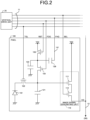
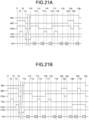
- the adjustment voltage is applied to the capacitive coupling wiring 141 (FHG) when the coupling unit 104 is in the non-conductive state.
- the potential of the first charge retaining unit 121 rises.
- the charge retention capacity of the first charge retaining unit 121 can be increased.
- no adjustment voltage is applied to the second charge retaining unit 122.
- the potential of the second charge retaining unit 122 is maintained at a low state.
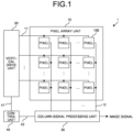
- the reset signal "f” and the image signal “e” in the low-sensitivity mode are further generated and retained in the column signal processing unit 30.
- the column signal processing unit 30 executes CDS in the low-sensitivity mode. Specifically, the column signal processing unit 30 subtracts the reset signal "f” from the image signal "e” to remove an offset error of the image signal in the low-sensitivity mode.
- an adjustment signal is applied to a signal line FHG.
- the application of the adjustment voltage to the signal line FHG continues until T23 in the drawing.
- an adjustment signal of a high voltage is applied to the charge retaining unit even during an exposure period. Note that the charge overflowed from the photoelectric conversion unit 101 during a period from T4 to T10 is retained in the first charge retaining unit 121.
- the ON voltage is applied to the signal line RST. Since the coupling unit 104 and the second charge transfer unit 106 are in the conductive state, the first charge retaining unit 121, the second charge retaining unit 122, and the third charge retaining unit 123 are reset.
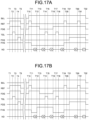
- image signals can be generated as in FIG. 18A .
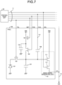
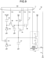
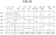
- FIG. 21B is a diagram illustrating another example of generation of image signals according to the eighth embodiment of the disclosure. Similarly to FIG. 18B , the drawing is a timing chart illustrating an example of generation of image signals in the pixel 100 in a case where the circuit of FIGS. 9 and 10 is adopted. Parts different from the generation procedure of FIG. 18B will be described.
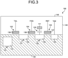
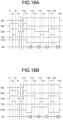
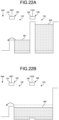
- the potential immediately below the gate of the reset unit 103 while being non-conductive is made deep, when the charge of the second photoelectric conversion unit 105 retained in the third charge retaining unit 123 is transferred to the charge retaining unit, a part of the charge is discharged by the reset unit 103. This causes an error in the image signal in the low-sensitivity mode. Therefore, the potential of the third charge retaining unit 123 is increased to increase the charge retention capacity of the third charge retaining unit 123. This makes it possible to prevent the reset unit 103 from discharging the charge retained in the third charge retaining unit 123. This process will be described with reference to FIGS. 22A and 22B .
Landscapes
- Engineering & Computer Science (AREA)
- Multimedia (AREA)
- Signal Processing (AREA)
- Solid State Image Pick-Up Elements (AREA)
- Transforming Light Signals Into Electric Signals (AREA)
Applications Claiming Priority (2)
| Application Number | Priority Date | Filing Date | Title |
|---|---|---|---|
| JP2020219267A JP2022104203A (ja) | 2020-12-28 | 2020-12-28 | 撮像素子及び撮像装置 |
| PCT/JP2021/046700 WO2022145254A1 (ja) | 2020-12-28 | 2021-12-17 | 撮像素子及び撮像装置 |
Publications (2)
| Publication Number | Publication Date |
|---|---|
| EP4270933A1 true EP4270933A1 (de) | 2023-11-01 |
| EP4270933A4 EP4270933A4 (de) | 2024-05-22 |
Family
ID=82259322
Family Applications (1)
| Application Number | Title | Priority Date | Filing Date |
|---|---|---|---|
| EP21915115.6A Pending EP4270933A4 (de) | 2020-12-28 | 2021-12-17 | Bildgebungselement und bildgebungsvorrichtung |
Country Status (5)
| Country | Link |
|---|---|
| US (2) | US12231795B2 (de) |
| EP (1) | EP4270933A4 (de) |
| JP (1) | JP2022104203A (de) |
| CN (1) | CN116636009A (de) |
| WO (1) | WO2022145254A1 (de) |
Family Cites Families (10)
| Publication number | Priority date | Publication date | Assignee | Title |
|---|---|---|---|---|
| JP4828914B2 (ja) | 2005-10-28 | 2011-11-30 | 株式会社東芝 | 固体撮像装置およびその駆動方法 |
| JP5664175B2 (ja) * | 2010-11-29 | 2015-02-04 | ソニー株式会社 | 固体撮像装置とその駆動方法、及び電子機器 |
| JP5637384B2 (ja) * | 2010-12-15 | 2014-12-10 | ソニー株式会社 | 固体撮像素子および駆動方法、並びに電子機器 |
| JP6024103B2 (ja) | 2011-06-30 | 2016-11-09 | ソニー株式会社 | 撮像素子、撮像素子の駆動方法、撮像素子の製造方法、および電子機器 |
| JP2015056878A (ja) * | 2013-09-13 | 2015-03-23 | 株式会社東芝 | 固体撮像装置 |
| TWI754696B (zh) * | 2016-12-14 | 2022-02-11 | 日商索尼半導體解決方案公司 | 固體攝像元件及電子機器 |
| KR102651415B1 (ko) * | 2017-02-20 | 2024-03-28 | 에스케이하이닉스 주식회사 | 이미지 센서 및 그 동작방법 |
| CN117577652A (zh) | 2017-06-02 | 2024-02-20 | 索尼半导体解决方案公司 | 固态摄像装置和电子设备 |
| CN117459846A (zh) * | 2018-09-19 | 2024-01-26 | 索尼半导体解决方案公司 | 固体摄像元件和电子设备 |
| EP3896966B1 (de) * | 2018-12-11 | 2024-09-04 | Sony Semiconductor Solutions Corporation | Bilderzeugende festkörpervorrichtung und elektronisches instrument |
-
2020
- 2020-12-28 JP JP2020219267A patent/JP2022104203A/ja active Pending
-
2021
- 2021-12-17 WO PCT/JP2021/046700 patent/WO2022145254A1/ja not_active Ceased
- 2021-12-17 EP EP21915115.6A patent/EP4270933A4/de active Pending
- 2021-12-17 US US18/035,032 patent/US12231795B2/en active Active
- 2021-12-17 CN CN202180086520.7A patent/CN116636009A/zh active Pending
-
2025
- 2025-02-17 US US19/055,304 patent/US20250234109A1/en active Pending
Also Published As
| Publication number | Publication date |
|---|---|
| US20230403483A1 (en) | 2023-12-14 |
| JP2022104203A (ja) | 2022-07-08 |
| WO2022145254A1 (ja) | 2022-07-07 |
| CN116636009A (zh) | 2023-08-22 |
| US12231795B2 (en) | 2025-02-18 |
| EP4270933A4 (de) | 2024-05-22 |
| US20250234109A1 (en) | 2025-07-17 |
Similar Documents
| Publication | Publication Date | Title |
|---|---|---|
| JP5369779B2 (ja) | 固体撮像装置、固体撮像装置の駆動方法および電子機器 | |
| CN104322053B (zh) | 图像传感器、驱动方法以及电子装置 | |
| CN101841635B (zh) | 固体成像设备、其驱动方法和电子装置 | |
| TWI628957B (zh) | 固態影像拾取裝置、其驅動方法以及電子設備 | |
| US9985060B2 (en) | Image pickup apparatus, image pickup system, and image pickup apparatus driving method | |
| JP6004665B2 (ja) | 撮像装置、および撮像システム。 | |
| JP2013031226A (ja) | Cmosイメージセンサのための、小サイズ、高利得及び低ノイズのピクセル | |
| JP2017130567A (ja) | 固体撮像素子および撮像装置 | |
| KR101760200B1 (ko) | 고체 촬상 소자 및 촬상 장치 | |
| JP6593435B2 (ja) | 固体撮像装置および固体撮像装置の駆動方法 | |
| US20250234109A1 (en) | Imaging element and imaging device | |
| JP7198675B2 (ja) | 固体撮像素子、その駆動回路および撮像装置 | |
| US20240276121A1 (en) | Imaging element and imaging device | |
| US20240334081A1 (en) | Imaging element and imaging device | |
| CN105308954B (zh) | 开关电路、采样保持电路以及固体摄像装置 | |
| JP2015076722A (ja) | 固体撮像素子および撮像装置 | |
| WO2022102404A1 (ja) | 固体撮像素子、電子機器および固体撮像素子の制御方法 |
Legal Events
| Date | Code | Title | Description |
|---|---|---|---|
| STAA | Information on the status of an ep patent application or granted ep patent |
Free format text: STATUS: THE INTERNATIONAL PUBLICATION HAS BEEN MADE |
|
| PUAI | Public reference made under article 153(3) epc to a published international application that has entered the european phase |
Free format text: ORIGINAL CODE: 0009012 |
|
| STAA | Information on the status of an ep patent application or granted ep patent |
Free format text: STATUS: REQUEST FOR EXAMINATION WAS MADE |
|
| 17P | Request for examination filed |
Effective date: 20230508 |
|
| AK | Designated contracting states |
Kind code of ref document: A1 Designated state(s): AL AT BE BG CH CY CZ DE DK EE ES FI FR GB GR HR HU IE IS IT LI LT LU LV MC MK MT NL NO PL PT RO RS SE SI SK SM TR |
|
| DAV | Request for validation of the european patent (deleted) | ||
| DAX | Request for extension of the european patent (deleted) | ||
| REG | Reference to a national code |
Ref country code: DE Ref legal event code: R079 Free format text: PREVIOUS MAIN CLASS: H04N0005374500 Ipc: H01L0027146000 |
|
| A4 | Supplementary search report drawn up and despatched |
Effective date: 20240422 |
|
| RIC1 | Information provided on ipc code assigned before grant |
Ipc: H04N 25/771 20230101ALI20240416BHEP Ipc: H04N 25/59 20230101ALI20240416BHEP Ipc: H01L 27/146 20060101AFI20240416BHEP |
|
| STAA | Information on the status of an ep patent application or granted ep patent |
Free format text: STATUS: EXAMINATION IS IN PROGRESS |
|
| 17Q | First examination report despatched |
Effective date: 20250617 |