EP4266312A1 - Ferroelektrischer speicher und speicheranordnung - Google Patents
Ferroelektrischer speicher und speicheranordnung Download PDFInfo
- Publication number
- EP4266312A1 EP4266312A1 EP21921894.8A EP21921894A EP4266312A1 EP 4266312 A1 EP4266312 A1 EP 4266312A1 EP 21921894 A EP21921894 A EP 21921894A EP 4266312 A1 EP4266312 A1 EP 4266312A1
- Authority
- EP
- European Patent Office
- Prior art keywords
- storage cell
- voltage
- capacitor
- ferroelectric
- line
- Prior art date
- Legal status (The legal status is an assumption and is not a legal conclusion. Google has not performed a legal analysis and makes no representation as to the accuracy of the status listed.)
- Granted
Links
Images







Classifications
-
- H—ELECTRICITY
- H10—SEMICONDUCTOR DEVICES; ELECTRIC SOLID-STATE DEVICES NOT OTHERWISE PROVIDED FOR
- H10B—ELECTRONIC MEMORY DEVICES
- H10B53/00—Ferroelectric RAM [FeRAM] devices comprising ferroelectric memory capacitors
- H10B53/30—Ferroelectric RAM [FeRAM] devices comprising ferroelectric memory capacitors characterised by the memory core region
-
- G—PHYSICS
- G11—INFORMATION STORAGE
- G11C—STATIC STORES
- G11C11/00—Digital stores characterised by the use of particular electric or magnetic storage elements; Storage elements therefor
- G11C11/21—Digital stores characterised by the use of particular electric or magnetic storage elements; Storage elements therefor using electric elements
- G11C11/22—Digital stores characterised by the use of particular electric or magnetic storage elements; Storage elements therefor using electric elements using ferroelectric elements
- G11C11/221—Digital stores characterised by the use of particular electric or magnetic storage elements; Storage elements therefor using electric elements using ferroelectric elements using ferroelectric capacitors
-
- G—PHYSICS
- G11—INFORMATION STORAGE
- G11C—STATIC STORES
- G11C11/00—Digital stores characterised by the use of particular electric or magnetic storage elements; Storage elements therefor
- G11C11/21—Digital stores characterised by the use of particular electric or magnetic storage elements; Storage elements therefor using electric elements
- G11C11/22—Digital stores characterised by the use of particular electric or magnetic storage elements; Storage elements therefor using electric elements using ferroelectric elements
- G11C11/225—Auxiliary circuits
- G11C11/2253—Address circuits or decoders
- G11C11/2255—Bit-line or column circuits
-
- G—PHYSICS
- G11—INFORMATION STORAGE
- G11C—STATIC STORES
- G11C11/00—Digital stores characterised by the use of particular electric or magnetic storage elements; Storage elements therefor
- G11C11/21—Digital stores characterised by the use of particular electric or magnetic storage elements; Storage elements therefor using electric elements
- G11C11/22—Digital stores characterised by the use of particular electric or magnetic storage elements; Storage elements therefor using electric elements using ferroelectric elements
- G11C11/225—Auxiliary circuits
- G11C11/2253—Address circuits or decoders
- G11C11/2257—Word-line or row circuits
-
- G—PHYSICS
- G11—INFORMATION STORAGE
- G11C—STATIC STORES
- G11C11/00—Digital stores characterised by the use of particular electric or magnetic storage elements; Storage elements therefor
- G11C11/21—Digital stores characterised by the use of particular electric or magnetic storage elements; Storage elements therefor using electric elements
- G11C11/22—Digital stores characterised by the use of particular electric or magnetic storage elements; Storage elements therefor using electric elements using ferroelectric elements
- G11C11/225—Auxiliary circuits
- G11C11/2259—Cell access
-
- G—PHYSICS
- G11—INFORMATION STORAGE
- G11C—STATIC STORES
- G11C11/00—Digital stores characterised by the use of particular electric or magnetic storage elements; Storage elements therefor
- G11C11/21—Digital stores characterised by the use of particular electric or magnetic storage elements; Storage elements therefor using electric elements
- G11C11/22—Digital stores characterised by the use of particular electric or magnetic storage elements; Storage elements therefor using electric elements using ferroelectric elements
- G11C11/225—Auxiliary circuits
- G11C11/2273—Reading or sensing circuits or methods
-
- G—PHYSICS
- G11—INFORMATION STORAGE
- G11C—STATIC STORES
- G11C11/00—Digital stores characterised by the use of particular electric or magnetic storage elements; Storage elements therefor
- G11C11/21—Digital stores characterised by the use of particular electric or magnetic storage elements; Storage elements therefor using electric elements
- G11C11/22—Digital stores characterised by the use of particular electric or magnetic storage elements; Storage elements therefor using electric elements using ferroelectric elements
- G11C11/225—Auxiliary circuits
- G11C11/2275—Writing or programming circuits or methods
-
- H—ELECTRICITY
- H10—SEMICONDUCTOR DEVICES; ELECTRIC SOLID-STATE DEVICES NOT OTHERWISE PROVIDED FOR
- H10B—ELECTRONIC MEMORY DEVICES
- H10B53/00—Ferroelectric RAM [FeRAM] devices comprising ferroelectric memory capacitors
- H10B53/20—Ferroelectric RAM [FeRAM] devices comprising ferroelectric memory capacitors characterised by the three-dimensional [3D] arrangements, e.g. with cells on different height levels
-
- H—ELECTRICITY
- H10—SEMICONDUCTOR DEVICES; ELECTRIC SOLID-STATE DEVICES NOT OTHERWISE PROVIDED FOR
- H10B—ELECTRONIC MEMORY DEVICES
- H10B53/00—Ferroelectric RAM [FeRAM] devices comprising ferroelectric memory capacitors
- H10B53/50—Ferroelectric RAM [FeRAM] devices comprising ferroelectric memory capacitors characterised by the boundary region between the core and peripheral circuit regions
-
- H—ELECTRICITY
- H10—SEMICONDUCTOR DEVICES; ELECTRIC SOLID-STATE DEVICES NOT OTHERWISE PROVIDED FOR
- H10D—INORGANIC ELECTRIC SEMICONDUCTOR DEVICES
- H10D1/00—Resistors, capacitors or inductors
- H10D1/60—Capacitors
- H10D1/68—Capacitors having no potential barriers
- H10D1/682—Capacitors having no potential barriers having dielectrics comprising perovskite structures
-
- G—PHYSICS
- G11—INFORMATION STORAGE
- G11C—STATIC STORES
- G11C11/00—Digital stores characterised by the use of particular electric or magnetic storage elements; Storage elements therefor
- G11C11/21—Digital stores characterised by the use of particular electric or magnetic storage elements; Storage elements therefor using electric elements
- G11C11/22—Digital stores characterised by the use of particular electric or magnetic storage elements; Storage elements therefor using electric elements using ferroelectric elements
- G11C11/225—Auxiliary circuits
- G11C11/2293—Timing circuits or methods
Definitions
- This application relates to the field of data storage technologies, and in particular, to a ferroelectric memory and a storage device.
- a ferroelectric random access memory may also be referred to as a ferroelectric memory.
- the ferroelectric memory is a memory made according to a principle that a polarization direction of a ferroelectric material changes under an action of electric field.
- one storage cell in the ferroelectric memory includes one transistor Q1 and one ferroelectric capacitor C1.
- the transistor Q1 includes a gate electrode G1, a source electrode S1, and a drain electrode D1.
- the ferroelectric capacitor C1 is formed on the gate electrode G1.
- the ferroelectric memory may include a substrate 101, a drain electrode D region 102, a source electrode S region 103, a channel CH region 104, a gate electrode layer 105, a ferroelectric layer 106, and an interface insulation layer 107.
- the interface insulation layer 107 may be located between the substrate 101 and the ferroelectric layer 106, and is configured to suppress an interface reaction between the substrate 101 and the ferroelectric layer 106 in a manufacturing process. Due to the interface reaction, a defect site capable of capturing a charge may be generated at a direct interface between the substrate 101 and the ferroelectric layer 106.
- a write voltage or a read voltage is applied between the gate electrode layer 105 and the substrate 101, a voltage drop across the interface insulation layer 107 is generated. Therefore, the write voltage or the read voltage needs to be increased to compensate for the voltage drop.
- the interface insulation layer 107 may be electrically damaged due to the increased write voltage or read voltage.
- a charge trap may be formed in the interface insulation layer 107 or at an interface between the interface insulation layer 107 and the channel CH region 104. This trap may be a leakage path that enables a charge to travel between the substrate 101 and the channel CH region 104. Consequently, the durability and reliability of a ferroelectric storage component are deteriorated.
- This application provides a ferroelectric memory and a storage device, to reduce an operating voltage and improve durability of the ferroelectric memory.
- a ferroelectric memory includes at least one storage cell, and each storage cell includes a transistor, a first ferroelectric capacitor, and at least one voltage divider capacitor.
- the transistor includes a gate electrode, a source electrode, and a drain electrode.
- One electrode of the first ferroelectric capacitor is connected to the gate electrode, and the other electrode of the first ferroelectric capacitor is connected to a word line.
- One electrode of each voltage divider capacitor in the at least one voltage divider capacitor is separately connected to the gate electrode, and the other electrode of each voltage divider capacitor in the at least one voltage divider capacitor is separately connected to the source electrode.
- the transistor may be a gate-all-around transistor.
- the transistor is a vertical nanowire transistor.
- the transistor includes a gate electrode, a channel, and a source electrode and a drain electrode that are located at two ends of the channel.
- the gate electrode may be a floating gate (Floating gate, FG).
- the floating gate may be in a floating (floating) state.
- the gate electrode is in a suspended state without a conductor out-lead, and is electrically suspended, that is, not connected to an external circuit.
- the channel may be columnar.
- the at least one voltage divider capacitor is included in each storage cell in the ferroelectric memory, and one electrode of each voltage divider capacitor in the at least one voltage divider capacitor is separately connected to the gate electrode.
- one electrode of the first ferroelectric capacitor is connected to one electrode of each voltage divider capacitor in the at least one voltage divider capacitor through the gate electrode, and the first ferroelectric capacitor is connected to the at least one voltage divider capacitor in series.
- the other electrode of each voltage divider capacitor in the at least one voltage divider capacitor is connected to the source electrode, and the at least one voltage divider capacitor is connected in parallel to the source electrode and the gate electrode of the transistor.
- the at least one voltage divider capacitor is connected in parallel with a transistor capacitor of the transistor, and a total capacitance of the parallel transistor capacitor and the at least one voltage divider capacitor increases.
- an operating voltage allocated to the transistor capacitor of the transistor decreases.
- a voltage allocated to the source electrode and the gate electrode of the transistor decreases, and an operating voltage allocated to the first ferroelectric capacitor increases.
- the operating voltage allocated to the first ferroelectric capacitor that is connected in series to the at least one voltage divider capacitor is increased by disposing the at least one voltage divider capacitor.
- the first ferroelectric capacitor may reach a polarization state with a smaller operating voltage. For example, in a conventional technology, a 3 V operating voltage is required to electrically polarize the first ferroelectric capacitor.
- the operating voltage allocated to the first ferroelectric capacitor increases, so that a smaller operating voltage, for example, 2 V, can electrically polarize the first ferroelectric capacitor and the operating voltage is reduced.
- the formation of the trap facilitating current leakage in the interface insulation layer or at the interface that is between the interface insulation layer and the channel is avoided, to avoid that a charge captured by the trap escapes from the trap, and avoid a loss of a stored charge caused by the formed charge leakage path.
- This improves a charge retention force, and improves a charge storage capability of the ferroelectric memory.
- the charge storage capability determines a storage window of the ferroelectric memory. In this way, performance of the ferroelectric memory, for example, the storage window, is improved.
- the voltage divider capacitor is a high-dielectric-constant capacitor or a ferroelectric capacitor.
- the high-dielectric-constant capacitor may use a high-dielectric-constant material as a dielectric material of the capacitor, and the ferroelectric capacitor may use a ferroelectric material as a dielectric material of the capacitor.
- the high-dielectric-constant (high-k) material is a type of polymer material with a high dielectric constant, and may be a material whose dielectric constant is greater than that of silicon dioxide.
- the dielectric constant of silicon dioxide is 3.9.
- the high-dielectric-constant material includes, for example, tantalum pentaoxide, titanium oxide, and barium strontium titanate.
- the ferroelectric material is a material that has spontaneous electric polarization without applying an external electric field. Specifically, the ferroelectric material may maintain any one of two stable remanent polarization (remanent polarization) states. These features can be used in a storage device to store logical information "0" or "1" in a non-volatile manner.
- Ferroelectric materials include barium titanate (BaTiO 3 ), potassium dihydrogen phosphate (KH 2 PO 4 ), and the like.
- the voltage divider capacitor may be a high-dielectric-constant capacitor.
- the high-dielectric-constant capacitor is connected in parallel to the transistor, so that a voltage allocated to the transistor is reduced, and the voltage allocated to the first ferroelectric capacitor is increased.
- a structure of the ferroelectric memory can reduce the operating voltage, reduce the interface defect in the ferroelectric memory, improve the durability and reliability of the ferroelectric memory, and enlarge the storage window.
- the voltage divider capacitor may be a ferroelectric capacitor.
- the ferroelectric capacitor is connected in parallel to the transistor, so that the voltage allocated to the transistor is reduced, and the voltage allocated to the first ferroelectric capacitor is increased. Therefore, a larger storage window can be implemented under a same operating voltage.
- the structure of the ferroelectric memory can reduce the operating voltage, reduce the interface defect in the ferroelectric memory, and improve the durability and reliability of the ferroelectric memory.
- the ferroelectric capacitor serves as a second ferroelectric capacitor. The second ferroelectric capacitor and the first ferroelectric capacitor form opposite polarization, to maintain charge balance of the gate electrode in the transistor, and reduce charge leakage between a substrate and the channel.
- the at least one voltage divider capacitor includes at least one first capacitor and at least one second capacitor.
- the first capacitor is a high-dielectric-constant capacitor
- the second capacitor is a ferroelectric capacitor.
- the at least one voltage divider capacitor may be a high-dielectric-constant capacitor.
- the at least one voltage divider capacitor may alternatively be a ferroelectric capacitor, and the at least one voltage divider capacitor includes a high-dielectric-constant capacitor and a ferroelectric capacitor.
- the transistor capacitor is connected in parallel to a plurality of voltage divider capacitors to increase the total capacitance, to reduce a voltage allocated to a total capacitor and increase the voltage allocated to the first ferroelectric capacitor.
- the structure of the ferroelectric memory can reduce the operating voltage, reduce the interface defect in the ferroelectric memory, improve the durability and reliability of the ferroelectric memory, and enlarge the storage window.
- the ferroelectric memory further includes a bit line, a source line, and a word line.
- the source line is connected to the source electrode
- the bit line is connected to the drain electrode
- the word line is connected to the other electrode of the first ferroelectric capacitor.
- different voltages are separately applied to the bit line, the source line, and the word line, so that reading and writing on the storage cell can be implemented.
- the ferroelectric memory further includes a first voltage line, a second voltage line, and a third voltage line.
- One end of the first voltage line is connected to the source electrode
- one end of the second voltage line is connected to the drain electrode
- one end of the third voltage line is connected to the other electrode of the first ferroelectric capacitor
- the other ends of the first voltage line, the second voltage line, and the third voltage line are separately connected to a controller, to receive a read and write control voltage.
- different voltages are separately applied to the first voltage line, the second voltage line, and the third voltage line, so that reading and writing on the storage cell can be implemented.
- the at least one storage cell includes a first storage cell.
- a voltage difference between the first voltage line and the second voltage line of the first storage cell is 0, and an absolute value of a voltage difference between the third voltage line and the second voltage line of the first storage cell is equal to a first specified voltage.
- data can be written into the first storage cell, and when the voltage difference between the source electrode and the drain electrode is equal to 0, a leakage current of a write operation can be suppressed.
- the at least one storage cell further includes a second storage cell.
- an absolute value of a voltage difference between the third voltage line and the second voltage line of the second storage cell is less than one half of the first specified voltage.
- the first voltage line, the second voltage line, and the third voltage line of a second storage cell in the at least one storage cell are all in the floating state. In the foregoing possible implementation, it can be ensured that the status of the second storage cell is not affected in the data writing process.
- bias voltages of the first voltage line, the second voltage line, and the third voltage line of the second storage cell in the at least one storage cell are all one half of the first specified voltage.
- a bias voltage of the first voltage line of the first storage cell is 0, a bias voltage of the second voltage line of the first storage cell is a second specified voltage, and a bias voltage of the third voltage line of the first storage cell is a third specified voltage.
- data reading in the first storage cell can be implemented, and it can be ensured that the data in the first storage cell is consistent before and after a reading operation after the data reading is completed.
- the third voltage line of the second storage cell in the at least one storage cell is in the floating state or grounded. In the foregoing possible implementation, it can be ensured that a status of an unselected second storage cell is not affected in the data reading process.
- the bias voltages of the first voltage line and the second voltage line of the second storage cell in the at least one storage cell are both 0. In the foregoing possible implementation, it can be ensured that the status of the unselected second storage cell is not affected in the data reading process.
- a storage device includes a circuit board and a ferroelectric memory connected to the circuit board, and the ferroelectric memory is the ferroelectric memory provided in any one of the first aspect or the possible implementations of the first aspect.
- a storage device includes a controller and a ferroelectric memory.
- the controller is configured to control reading and writing of the ferroelectric memory, and the ferroelectric memory is the ferroelectric memory provided in any one of the first aspect or the possible implementations of the first aspect.
- any storage device provided above a non-transitory computer-readable storage medium used with a computer, and the like include a same or corresponding feature of the ferroelectric memory provided above. Therefore, for beneficial effects that can be achieved, refer to beneficial effects of the corresponding integrated circuit provided above. Details are not described herein again.
- circuits or another component may be described as or referred to as “configured to” perform one or more tasks.
- “configured to” is used to imply a structure by indicating that the circuit/component includes a structure (for example, a circuit system) that performs one or more tasks during operation. Therefore, the circuit/component can be referred to as being configured to perform the task even when the specified circuit/component is not currently operational (for example, is not on).
- the circuit/component used with the term “configured to” includes hardware, for example, a circuit that performs an operation.
- At least one of a, b, or c may represent: a, b, c, a and b, a and c, b and c, or a, b, and c, where a, b, and c may be singular or plural.
- the terms such as “first” and “second” are not intended to limit a quantity or an execution sequence.
- connection includes one or more of “mechanical connection”, “electrical connection”, and “communication connection”.
- connection includes one or more of “mechanical connection”, “electrical connection”, and “communication connection”.
- connection includes one or more of “mechanical connection”, “electrical connection”, and “communication connection”.
- connection includes one or more of “mechanical connection”, “electrical connection”, and “communication connection”.
- the element can be directly connected “above” or “below” the another element, or may be indirectly connected “above” or “below” the another element through an intermediate element.
- the technical solutions of this application may be applied to various storage systems using ferroelectric memories.
- the technical solutions of this application may be applied to a computer, or may be applied to a storage system including a memory or a storage system including a processor and a memory.
- the processor may be a central processing unit (central processing unit, CPU), an artificial intelligence (artificial intelligence, AI) processor, a digital signal processor (digital signal processor), a neural network processor, or the like.
- FIG. 2 is a schematic diagram of a structure of a storage system according to an embodiment of this application.
- the storage system may include the ferroelectric memory.
- the storage system may further include a CPU, a cache (cache), a controller, and the like.
- the CPU, the cache, the controller, and the ferroelectric memory may be integrated together.
- the ferroelectric memory may be coupled to the cache by using the controller, and may be coupled to the CPU by using the cache.
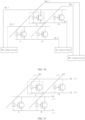
- FIG. 3 is a schematic diagram of a structure of a ferroelectric memory according to an embodiment of this application.
- the ferroelectric memory may include at least one storage cell, a first voltage line, a second voltage line, and a third voltage line.
- One storage cell may be a cell configured to store 1-bit data.
- the ferroelectric memory includes a storage cell array with m rows and n columns, m first voltage lines, m second voltage lines, and n third voltage lines.
- the storage cell array includes at least one storage cell, and m and n are positive integers.
- FIG. 3 an example in which values of m and n are both equal to 2 is used for description.
- An example in which the at least one storage cell includes four storage cells is used for description.
- the plurality of storage cells may be located at a same layer, or may be disposed on different layers by stacking.
- a first storage cell A, a second storage cell B, a third storage cell C, and a fourth storage cell D are located at a same layer, as shown in FIG. 3 , the first storage cell A and the second storage cell B are located in a same row, the third storage cell C and the fourth storage cell D are located in a same row, the first storage cell A and the third storage cell C are located in a same column, and the second storage cell B and the fourth storage cell D are located in a same column.
- First voltage lines of storage cells in a same row may be connected to each other, second voltage lines of storage cells in a same row may be connected to each other, and third voltage lines of storage cells in a same column may be connected to each other.
- a first voltage line of the first storage cell A may be connected to a first voltage line of the second storage cell B
- a second voltage line of the first storage cell A may be connected to a second voltage line of the second storage cell B.
- a first voltage line and a second voltage line of the third storage cell C may be connected to a first voltage line and a second voltage line of the fourth storage cell D respectively.
- a third voltage line of the first storage cell A may be connected to a third voltage line of the third storage cell C
- a third voltage line of the second storage cell B may be connected to a third voltage line of the fourth storage cell D.
- the plurality of storage cells in the at least one storage cell may be located at different layers.
- the first storage cell A and the second storage cell B are located at a first layer
- the third storage cell C and the fourth storage cell D are located at a second layer.
- the first voltage lines of the storage cells at the first layer and the second layer may be multiplexed, to be specific, the storage cells at the first layer and the second layer share a same first voltage line.
- the second voltage lines of the storage cells at the first layer and the second layer may be multiplexed, to be specific, the storage cells at the first layer and the second layer share a same second voltage line.
- the third voltage lines of the storage cells at the first layer and the second layer may be multiplexed, to be specific, the storage cells at the first layer and the second layer share a same third voltage line.
- the ferroelectric memory when the storage cells are disposed on different layers by stacking, the ferroelectric memory further includes an isolation layer disposed between the first-layer storage cell and the second-layer storage cell, so that each storage cell has a first voltage line, a second voltage line, and a third voltage line that are independent.
- the foregoing manner of sharing the first voltage line, the second voltage line, or the third voltage line can reduce a quantity of connection lines of the first voltage line, the second voltage line, or the third voltage line, and ensure that layout area overheads are small.
- sharing the first voltage line, the second voltage line, or the third voltage line can reduce manufacturing costs.
- a manufacturing process of the storage cell is simple, and may be integrated into a back-end-of-line process, to implement high area efficiency of the storage cell and a control circuit in a three-dimensional stacking manner.
- the foregoing manner of disposing the isolation layer can also ensure that the layout area overheads are small.
- the first voltage line is connected to a source electrode of each storage cell
- the second voltage line is connected to a drain electrode of each storage cell
- the third voltage line is connected to a gate electrode of each storage cell, that is, connected to the other electrode of a first ferroelectric capacitor of each storage cell.
- the first voltage line may be a source line (source line, SL)
- the second voltage line may be a bit line (bit line, BL)
- the third voltage line may be a word line (word line, WL).
- the source line is connected to the source electrode of each storage cell
- the bit line is connected to the drain electrode of each storage cell
- the word line is connected to the other electrode of the first ferroelectric capacitor of each storage cell.
- a first voltage line connected to the storage cell is parallel to a second voltage line connected to the storage cell, the first voltage line connected to the storage cell is perpendicular to a third voltage line connected to the storage cell, and the second voltage line connected to the storage cell is perpendicular to the third voltage line connected to the storage cell.
- the following uses one storage cell in the storage cell array of the ferroelectric memory as an example to describe a structure of the storage cell in detail.
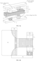
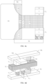
- FIG. 4a is a three-dimensional diagram of a storage cell according to an embodiment of this application.
- the storage cell includes a transistor Q, a first ferroelectric capacitor C F , and at least one voltage divider capacitor C I .
- the transistor Q includes a gate electrode G, a channel CH, and a source electrode S and a drain electrode D that are located at two ends of the channel CH.
- One electrode (namely, a first electrode) of the first ferroelectric capacitor C F is connected to the gate electrode G, and the other electrode (namely, a second electrode) of the first ferroelectric capacitor C F is connected to a word line WL.
- each voltage divider capacitor C ⁇ in the at least one voltage divider capacitor C I is connected to the gate electrode G, and the other electrode (namely, a second electrode) of each voltage divider capacitor C ⁇ in the at least one voltage divider capacitor C I is connected to the source electrode S.
- the second electrode of each voltage divider capacitor C I in the at least one voltage divider capacitor C ⁇ may be connected to the source electrode S through a metal trace (for example, a first voltage line) and a via T.
- the transistor Q in the storage cell may be a gate-all-around (gate-all-around, GAA) transistor, the gate electrode G may be in a floating (floating) state. To be specific, the gate electrode G is in a suspended state without a conductor out-lead.
- the channel CH may be columnar.
- the transistor Q may alternatively be a transistor of another structure or type. This is not specifically limited in this embodiment of this application. In this embodiment of this application, only an example in which the transistor Q is a GAA transistor is used for description.
- the gate electrode G of the transistor Q is connected to a third voltage line (word line WL) through the first ferroelectric capacitor C F , the drain electrode D of the transistor Q is connected to a second voltage line (bit line BL), and the source electrode S of the transistor Q is connected to a first voltage line (source line SL).
- the first ferroelectric capacitor C F includes two electrodes and a dielectric material c located between the two electrodes, where the two electrodes include a first electrode a and a second electrode b.
- the storage cell includes a substrate SU, the channel CH, the source electrode S, the drain electrode D, the gate electrode G, the first ferroelectric capacitor C F , the voltage divider capacitor C I , and an insulation layer I between the gate electrode G and the channel CH.
- That the first electrode a of the first ferroelectric capacitor C F is connected to the gate electrode G of the transistor Q may be that the first electrode a of the first ferroelectric capacitor C F is formed on the gate electrode G, and the gate electrode G is directly used as the first electrode a of the first ferroelectric capacitor C F .
- the first electrode a of the first ferroelectric capacitor C F is connected to the gate electrode G of the transistor Q may be that one first metal plate is formed on the gate electrode G, the first metal plate is used as the first electrode a of the first ferroelectric capacitor C F , and the first metal plate is connected to the gate electrode G.
- the second electrode b of the first ferroelectric capacitor C F may be one second metal plate formed on the dielectric material c, and the first ferroelectric capacitor C F is connected to the word line WL through the second metal plate.
- the dielectric material c is a material characterized by electric polarization, and is an electrical insulating material.
- the dielectric material c does not have a long-distance drift of carriers under action of an electric field, but still has an electric phenomenon. This electric phenomenon is generated because charged particles also exist in the material. Although these charged particles are bound to a fixed position, charge gravity centers of positive and negative bounding no longer coincide under the action of the electric field, and electric polarization is caused.
- the electric polarization is a phenomenon that under the action of the electric field, a bound charge in the dielectric material c shifts or a polarity rotates in a direction of the electric field, in other words, a phenomenon that centers of a positive charge and a negative charge in a molecule relatively shift under the action of the electric field to generate an electric dipole moment.
- the dielectric material c includes a ferroelectric material.
- the ferroelectric material means that a lattice structure of the material has a spontaneous polarization phenomenon without an external electric field, and a direction of the spontaneous polarization of the material can be reversed or redirected by the external electric field. This feature of the ferroelectric material is also referred to as " ferroelectric phenomena " or "ferroelectric effect". When there is no external electric field action, polarization generated due to ordered arrangement of electric dipoles exists in the lattice. This is referred to as spontaneous polarization. Specifically, the ferroelectric material may maintain any one of two stable remanent polarization (remanent polarization) states.
- Ferroelectric materials may include barium titanate (BaTiO 3 ), potassium dihydrogen phosphate (KH 2 PO 4 ), and the like.
- each voltage divider capacitor C I in the at least one voltage divider capacitor C I includes two electrodes and a dielectric material c located between the two electrodes, where the two electrodes include a first electrode a and a second electrode b.
- An example in which the at least one voltage divider capacitor C ⁇ includes one voltage divider capacitor C I is used for description.
- that the first electrode a of the voltage divider capacitor C ⁇ is connected to the gate electrode G of the transistor Q may be that the first electrode a of the voltage divider capacitor C I is formed on the gate electrode G, and the gate electrode G is directly used as the first electrode a of the voltage divider capacitor C I .
- FIG. 4b that the first electrode a of the voltage divider capacitor C ⁇ is connected to the gate electrode G of the transistor Q may be that the first electrode a of the voltage divider capacitor C I is formed on the gate electrode G, and the gate electrode G is directly used as the first electrode a of the voltage divider capacitor C I .
- FIG. 4b that the first electrode a of the
- the first electrode a of the voltage divider capacitor C I is connected to the gate electrode G of the transistor Q may be that one first metal plate is formed on the gate electrode G, the first metal plate is used as the first electrode a of the voltage divider capacitor C I , and the first metal plate is connected to the gate electrode G.
- the second electrode b of the voltage divider capacitor C I may be one second metal plate formed on the dielectric material c, and the voltage divider capacitor C ⁇ is connected to the word line WL through the second metal plate.
- the first electrode a of the first ferroelectric capacitor C F and the first electrode a of each voltage divider capacitor C ⁇ in the at least one voltage divider capacitor C ⁇ are separately connected to the gate electrode G.
- the first ferroelectric capacitor C F and the voltage divider capacitor C I are separately formed on two surfaces that are disposed opposite to each other and that are of the gate electrode G.
- the first ferroelectric capacitor C F is formed on a surface that is of the gate electrode G and that is away from the source electrode S
- the voltage divider capacitor C I is formed on a surface that is of the gate electrode G and that is close to the source electrode S.
- the first electrode a of the first ferroelectric capacitor C F and the first electrode a of each voltage divider capacitor C I in the at least one voltage divider capacitor C I are separately connected to two ends of the gate electrode G.
- the at least one voltage divider capacitor C I may include a plurality of voltage divider capacitors C I .
- FIG. 4d An example in which the at least one voltage divider capacitor C I includes two voltage divider capacitors C I is used for description.
- the at least one voltage divider capacitor C ⁇ includes a first capacitor C I1 and a second capacitor C I2 .
- a first electrode a of the first capacitor C I1 is connected to the gate electrode G, and a second electrode b of the first capacitor C I1 is connected to the source electrode S of the transistor Q. That is, the second electrode b of the first capacitor C I1 is connected to the source line SL.
- a first electrode a of the second capacitor C I2 is connected to the gate electrode G, and a second electrode b of the second capacitor C I2 is connected to the source electrode S of the transistor Q. That is, the second electrode b of the second capacitor C I2 is connected to the source line SL.
- the first capacitor C I1 may be a ferroelectric capacitor, and the second capacitor C I2 may be a high-dielectric-constant capacitor.
- each voltage divider capacitor C ⁇ in the at least one voltage divider capacitor C I may be a high-dielectric-constant capacitor or a ferroelectric capacitor.
- each voltage divider capacitor C I in the at least one voltage divider capacitor C I is a high-dielectric-constant capacitor.
- each voltage divider capacitor C I in the at least one voltage divider capacitor C I is a ferroelectric capacitor.
- the at least one voltage divider capacitor C I includes at least one first capacitor C I1 and at least one second capacitor C I2 , where the first capacitor C I1 is a high-dielectric-constant capacitor, and the second capacitor C I2 is a ferroelectric capacitor.
- the high-dielectric-constant capacitor may use a high-dielectric-constant material as a dielectric material of the capacitor, and the ferroelectric capacitor may use a ferroelectric material as a dielectric material of the capacitor.
- a dielectric constant permittivity
- the dielectric constant may represent a physical quantity of a capability of polarization and charge storage.
- the dielectric constant is for measuring performance of an insulator for storing electric energy.
- the dielectric constant is a ratio of capacitance between two metal plates when an insulating material is used as the medium to capacitance between same two metal plates when air is used as the medium or vacuum is used.
- the high-dielectric-constant (high-k) material is a type of polymer material with a high dielectric constant, and may be a material whose dielectric constant is greater than that of silicon dioxide.
- the dielectric constant of silicon dioxide is 3.9.
- a material whose dielectric constant is greater than 3.9 is referred to as a high dielectric material.
- a material whose dielectric constant is greater than that of Si 3 N 4 is referred to as the high-dielectric-constant material, that is, a material whose dielectric constant is greater than 7 is referred to as the high dielectric material.
- a material whose dielectric constant k is less than that of SiO 2 is referred to as a low-dielectric-constant material, that is, a material whose dielectric constant is less than 3.9 is referred to as a low dielectric material.
- the high-dielectric-constant material may include, for example, tantalum pentaoxide, titanium oxide, and barium strontium titanate.
- electrodes of the first ferroelectric capacitor C F and the voltage divider capacitor C I include a compound.
- the compound may include a first metal element and a second metal element in an element periodic table, where the first metal element may be selected from a group that includes Ir and Ru.
- the electrode may be a compound of silicon and metal, for example, titanium, tungsten, titanium nitride (TiN), aluminum titanium nitride (TiAlN), or silicon titanium nitride (TiSiN).
- two ends of the gate electrode G of the storage cell are respectively connected to the first ferroelectric capacitor C F and one voltage divider capacitor C ⁇ for description.
- FIG. 5 is a circuit diagram of a storage cell according to an embodiment of this application.
- Each storage cell includes a transistor Q, a first ferroelectric capacitor C F , and a voltage divider capacitor C I .
- the transistor Q includes a source electrode S, a drain electrode D, and a gate electrode G.
- the source electrode S is connected to a source line SL
- the drain electrode D is connected to a bit line BL
- the gate electrode G is connected to a word line WL through the first ferroelectric capacitor C F
- the gate electrode G is connected to the source line SL through the voltage divider capacitor C I .
- the gate electrode G of the transistor Q may be used as one electrode, the source electrode S, the drain electrode D, and a substrate SU may be used as one electrode, and an insulation layer I or a reverse bias PN junction in the transistor Q may be used as a dielectric material.
- the transistor Q may be considered as a capacitor, and the storage cell includes the capacitor of the transistor Q.
- the capacitor of the transistor Q is referred to as a transistor capacitor C MOS .
- the transistor capacitor C MOS includes a first electrode and a second electrode.
- the gate electrode G of the transistor Q is used as the first electrode, and the source electrode S, the drain electrode D, and the substrate SU of the transistor Q are used as the second electrode.
- the storage cell includes the first ferroelectric capacitor C F , the voltage divider capacitor C I , and the transistor capacitor C MOS , where the voltage divider capacitor C I may be a high-dielectric-constant capacitor or a ferroelectric capacitor.
- a first electrode of the first ferroelectric capacitor C F is connected to the word line WL, and a second electrode of the first ferroelectric capacitor C F is connected to a first electrode of the voltage divider capacitor C I and the first electrode of the transistor capacitor C MOS , that is, the gate electrode G of the transistor Q.
- the second electrode of the transistor capacitor C MOS is connected to the source line SL.
- the first electrode of the voltage divider capacitor C ⁇ is connected to the second electrode of the first ferroelectric capacitor C F and the first electrode of the transistor capacitor C MOS , and a second electrode of the voltage divider capacitor C I is connected to the source line SL.
- the voltage divider capacitor C I is connected between the gate electrode G and the source electrode S of the transistor Q.
- the voltage divider capacitor C I is connected in parallel to the transistor capacitor C MOS .
- the voltage divider capacitor C I is connected in series to the first ferroelectric capacitor C F .
- V F V WL ⁇ V SL C F C MOS + C I + C F
- the at least one voltage divider capacitor includes a plurality of voltage divider capacitors
- the voltage allocated to the first ferroelectric capacitor C F increases, so that the operating voltage can be further reduced, the durability and stability of the storage cell can be further improved, and the durability and stability of the ferroelectric memory can be further improved.
- the storage cell includes a second ferroelectric capacitor C F1 , and the first ferroelectric capacitor C F and the second ferroelectric capacitor C F1 are connected to the gate electrode G of the storage cell.
- the word line WL is set to 0 potential
- the source line SL and the bit line BL are set to a first specified voltage Vw.
- the first specified voltage Vw may be 2 V.
- An electric field is applied to the first ferroelectric capacitor C F through the word line WL, and the first ferroelectric capacitor C F generates a polarization phenomenon.
- a positive charge is induced at a part that is of the gate electrode G and that is close to the first ferroelectric capacitor C F
- a negative charge is induced at a part that is of the gate electrode G and that is away from the first ferroelectric capacitor C F
- a positive charge is induced at a part that is of the second ferroelectric capacitor C F1 and that is close to the gate electrode G
- a negative charge is induced at a part that is of the second ferroelectric capacitor C F1 and that is away from the gate electrode G.
- charge distribution of the first ferroelectric capacitor C F is different from that of the second ferroelectric capacitor C F1 .
- the word line WL is set to the first specified voltage Vw, for example, 2 V, and the source line SL and the bit line BL are set to 0 potential.
- An electric field is applied to the first ferroelectric capacitor C F through the word line WL, and the first ferroelectric capacitor C F generates a polarization phenomenon. If a negative charge is induced at a part that is of the first ferroelectric capacitor C F and that is close to the word line WL, a positive charge is induced at a part that is of the first ferroelectric capacitor C F and that is away from the word line WL.
- a negative charge is induced at a part that is of the gate electrode G and that is close to the first ferroelectric capacitor C F
- a positive charge is induced at a part that is of the gate electrode G and that is away from the first ferroelectric capacitor C F
- a negative charge is induced at a part that is of the second ferroelectric capacitor C F1 and that is close to the gate electrode G
- a positive charge is induced at a part that is of the second ferroelectric capacitor C F1 and that is away from the gate electrode G.
- charge distribution of the first ferroelectric capacitor C F is different from that of the second ferroelectric capacitor C F1 .
- the first ferroelectric capacitor C F and the second ferroelectric capacitor C F1 in the storage cell generate opposite polarization, and based on electrostatic induction, charges in the gate electrode G are balanced, and electric neutrality is maintained. This avoids charge leakage and avoids current leakage.
- FIG. 7c is a schematic diagram of hysteresis curves of a first ferroelectric capacitor and a second ferroelectric capacitor according to an embodiment of this application.
- V represents an applied voltage on a WL corresponding to a storage cell
- P represents polarization strength of a corresponding ferroelectric capacitor.
- a curve 1 is a hysteresis curve of the first ferroelectric capacitor C F
- a curve 2 is a hysteresis curve of the second ferroelectric capacitor C F1 .
- the curve 1 is a hysteresis curve of the second ferroelectric capacitor C F1
- the curve 2 is a hysteresis curve of the first ferroelectric capacitor C F .
- the storage cell when at least one voltage divider capacitor includes one ferroelectric capacitor, the storage cell includes the first ferroelectric capacitor C F , the second ferroelectric capacitor C F1 , and a transistor Q, that is, the storage cell is of a 1T2F (1 Transistor-2 Ferroelectric Capacitors) structure.
- the at least one voltage divider capacitor when the at least one voltage divider capacitor includes N-1 ferroelectric capacitors, the storage cell includes one first ferroelectric capacitor C F , N-1 second ferroelectric capacitors C F1 , and the transistor Q, that is, the storage cell is of a 1TNF (1 Transistor-N Ferroelectric Capacitors) structure.
- the storage cell includes the first ferroelectric capacitor, the high-dielectric-constant capacitor, and the transistor Q, that is, the storage cell is of a 1T1FC (1 Transistor-1 Ferroelectric & 1 Conventional Capacitor) structure.
- the at least one voltage divider capacitor includes N high-dielectric-constant capacitors
- the storage cell includes the first ferroelectric capacitor, N high-dielectric-constant capacitors, and the transistor Q, that is, the storage cell is of a 1 T1FNC (1 Transistor-1 Ferroelectric & NConventional Capacitor) structure.
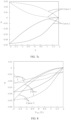
- FIG. 8 is a schematic diagram of hysteresis curve comparison according to an embodiment of this application.
- a curve 1 is a hysteresis curve of a 1T1C structure.
- a curve 2 is a hysteresis curve of a 1T1FC structure.
- a curve 3 is a hysteresis curve of a 1T2F structure.
- V represents an applied voltage on a word line WL corresponding to a storage cell
- P represents polarization strength of a corresponding ferroelectric capacitor.
- FIG. 9 is a schematic diagram of comparison between storage windows according to an embodiment of this application.
- a curve 1 is a schematic curve of a current of a 1T1C structure.
- a curve 2 is a schematic curve of a current of a 1T1FC structure.
- a curve 3 is a schematic curve of a current of a 1T2F structure.
- V represents a voltage on a word line WL corresponding to a storage cell, that is, a voltage on a gate electrode G of a transistor Q
- Id represents a current on a bit line BL corresponding to the storage cell, that is, a drain electrode D current on the transistor Q.
- An example in which the voltage applied on the WL is 0 V is used for description.
- a current difference between two intersection points of the 1T1C structure and 0 V is less than a current difference between two intersection points of the 1T2F structure and 0 V, and a current difference between two intersection points of the 1T2F structure and 0 V is less than a current difference between two intersection points of the 1T1FC structure and 0 V. It can be learned that a storage window of the 1T1C structure is smaller than a storage window of the 1T2F structure, and a storage window of the 1T2F structure is smaller than a storage window of the 1T1FC structure.
- a value of the storage window may be a ratio of a high impedance state of the ferroelectric capacitor to a low impedance state of the ferroelectric capacitor. For example, when the first ferroelectric capacitor is positively polarized, and "1" is written into, a relationship curve of a drain-source current (I d ) and a word line V WL is shifted to the right. When the first ferroelectric capacitor is negatively polarized, and "0" is written into, the relationship curve of the drain-source current (I d ) and the word line V WL is shifted to the left. The curve shifts, and a voltage on the word line V WL is shifted correspondingly. A size of the shift is the storage window.
- BLs for example, BL 0 and BL 1
- SLs for example, SL 0 and SL 1
- a source line SL connection and a bit line BL connection at different layers or a same layer are implemented by a metal trace and a via.
- word lines WLs at different layers or a same layer may be independent of each other.
- word lines WLs (for example, WL 0 and WL 1) at different layers or a same layer are connected to a WL control circuit having a gating function.
- the ferroelectric memory may be located at a metal wiring layer.
- the ferroelectric memory is formed by a back-end-of-line process, so that the ferroelectric memory and various controllers may be formed using a same process.
- the controller may control the voltages applied to the m first voltage lines, the m second voltage lines, and the n third voltage lines.
- the following provides descriptions by using an example in which the first voltage line is a source line SL, the second voltage line is a word line WL, and the third voltage line is a bit line BL.
- Bit lines BLs (for example, BL 1 and BL 2) of storage cells at a same layer may be connected to a same BL controller, sense amplifier, and the like.
- Source lines SLs (for example, SL 1 and SL 2) of storage cells at a same layer may be connected to a same SL controller.
- a source line SL connection and a bit line BL connection at a same layer are implemented by a metal trace and a via.
- word lines WLs at a same layer may be independent of each other.
- word lines WLs (for example, WL 1 and WL 2) at a same layer are connected to a WL control circuit having a gating function.
- the ferroelectric memory may be located at a metal wiring layer. In other words, the ferroelectric memory is formed by a back-end-of-line process, so that the ferroelectric memory and various controllers may be formed by a same process.
- different voltages are respectively applied to the source line SL, the bit line BL, and the word line WL by using a corresponding controller, or different voltages are respectively applied to the first voltage line, the second voltage line, and the third voltage line by using a corresponding controller, or different voltages are respectively applied to the source electrode S, the drain electrode D, and the first electrode of the first ferroelectric capacitor C F , so that reading and writing on the storage cell corresponding to the first ferroelectric capacitor can be implemented.
- the ferroelectric memory includes a storage cell array
- the storage cell array includes a first storage cell
- the first storage cell may be understood as a storage cell selected for writing data or reading data.
- both a source line SL and a bit line BL in the storage cell array may be set to be equipotential, that is, a voltage difference between the source line SL and the bit line BL is 0 (for example, a same voltage is applied to the source line SL and the bit line BL separately). In this way, a leakage current of a write operation can be suppressed.
- a voltage difference between the word line WL and the bit line BL that are connected to the storage cell in the storage cell array is set to implement writing of data "0" and "1". For example, when an absolute value of a voltage difference between a WL and a bit line BL that are connected to a storage cell is equal to the first specified voltage Vw, the storage cell is selected, the storage cell is written as data "1" or "0", and the storage cell is the first storage cell.
- a voltage difference between a word line WL and a bit line BL that correspond to a storage cell is equal to a positive first specified voltage Vw
- a ferroelectric material in the storage cell is positively polarized, and the storage cell is written as a "0" state.
- a voltage difference between a word line WL and a bit line BL that correspond to a storage cell is equal to a negative first specified voltage -Vw
- a ferroelectric material in the storage cell is negatively polarized, and the storage cell is written as a "1" state.
- the storage cell array includes a first storage cell A, a second storage cell B, a third storage cell C, and a fourth storage cell D is used for description.
- source lines SLs of all storage cells in a same row are connected together, and bit lines BLs of all storage cells in a same row are connected together.
- both a source line SL and a bit line BL in each storage cell in the storage cell array may be set to be equipotential.
- a source line SL and a bit line BL of each storage cell in a same row are set to be equipotential.
- source lines and bit lines of the first storage cell A and the second storage cell B that are in a same row are set to 0 V
- source lines and bit lines of the third storage cell C and the fourth storage cell D that are in a same row are set to 1 V.
- the first specified voltage Vw is applied to word lines WLs of the first storage cell A and the third storage cell C, for example, the first specified voltage Vw is 2 V, and a half of the first specified voltage 1/2Vw is applied to word lines WLs of the second storage cell B and the fourth storage cell D. Also refer to FIG. 12 .
- a voltage difference between a word line WL and a bit line BL that correspond to the first storage cell A is equal to the first specified voltage Vw, a dielectric material in the first storage cell A is positively polarized, and the first storage cell A is written as a "0" state.
- a voltage difference between a WL and a BL that correspond to the second storage cell B and a voltage difference between a WL and a BL that correspond to the third storage cell C are equal to 1/2Vw, that is, 1 V, and the second storage cell B and the third storage cell C are not selected to write data.
- a source line SL, a bit line BL, and a word line WL of the fourth storage cell D are all set to 1/2Vw, and the storage cell is not selected to write data.
- both a source line SL and a bit line BL in each storage cell in the storage cell array may be set to be equipotential.
- a source line SL and a bit line BL of each storage cell in a same row are set to be equipotential.
- source lines and bit lines of the first storage cell A and the second storage cell B that are in a same row are set to 2 V
- source lines and bit lines of the third storage cell C and the fourth storage cell D that are in a same row are set to 1 V.
- 0 V is applied to word lines WLs of the first storage cell A and the third storage cell C, and a half of the first specified voltage 1/2Vw, for example, 1 V, is applied to word lines WLs of the second storage cell B and the fourth storage cell D. Also refer to FIG. 14 .
- a voltage difference between a word line WL and a bit line BL that correspond to the first storage cell A is equal to a negative first specified voltage -Vw, that is, -2 V, a dielectric material in the first storage cell A is negatively polarized, and the first storage cell A is written as a "1" state.
- a voltage difference between a WL and a BL that correspond to the second storage cell B and a voltage difference between a WL and a BL that correspond to the third storage cell C are equal to a negative half of the first specified voltage 1/2Vw, that is, -1 V, and the second storage cell B and the third storage cell C are not selected to write data.
- a source line SL, a bit line BL, and a word line WL of the fourth storage cell D are all set to 1/2Vw, and the storage cell is not selected to write data.
- each selected storage cell in the 1T1FC/1T2F storage array structure provided in this embodiment of this application can be easily accessed.
- a source line SL and a bit line BL are set to be equipotential, to suppress a leakage current of a write operation.
- Vw for example, 2 V
- a ferroelectric thin film of the storage cell is positively polarized, and the storage cell is written as a "0" state; or when the voltage difference between the word line WL and the bit line BL of the storage cell is -Vw (for example, 2 V), the ferroelectric thin film of the storage cell is negatively polarized, and the storage cell is written as a "1" state.
- an absolute value of a voltage difference between a word line WL and a bit line BL that correspond to the another storage cell may be set to be less than 1/2Vw, to ensure that a state of the another storage cell remains unchanged.
- another storage cell other than the first storage cell is a second storage cell, that is, an unselected storage cell is the second storage cell.
- a source line SL, a bit line BL, and a word line WL that are in the second storage cell may all be set to 1/2Vw, or the source line SL, the bit line BL, and the word line WL that are in the second storage cell are enabled to be in a floating state, so that false writing in an unselected storage cell can be avoided.
- the first specified voltage Vw is greater than or equal to a critical voltage, where the critical voltage herein may be a critical voltage that reverses a polarization direction of the ferroelectric capacitor.
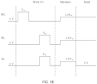
- the gate electrode G of the first storage cell needs to be precharged before the data is read, that is, the gate electrode G is charged to a potential, and the gate electrode G is held in a floating state. Then, a data reading operation is performed, that is, a source line SL of the storage cell is set to 0 potential, a bit line BL of the storage cell is set to a second specified voltage V BLR , and a word line WL of the storage cell is set to a third specified voltage V WLR .
- a source line SL of a first storage cell A is set to 0 potential
- a bit line BL of the first storage cell A is set to the second specified voltage V BLR , for example, 1 V
- a word line WL of the first storage cell A is set to the third specified voltage V WLR , for example, 1 V.
- the first storage cell A is the first storage cell.
- the source line SL of the second storage cell is set to 0 potential
- the bit line BL of the second storage cell B is set to the second specified voltage V BLR , for example, 1 V
- the word line WL of the second storage cell A is set to 0 potential.
- the source line SL and the bit line BL of the third storage cell C are set to be equipotential, for example, 1 V, and the word line WL of the third storage cell C is set to 1 V.
- the source line SL and the bit line BL of the fourth storage cell D are set to be equipotential, for example, 1 V, and the word line WL of the fourth storage cell D is set to 0 V. In this case, the second storage cell B, the third storage cell C, and the fourth storage cell D are not selected.
- a word line WL of the first storage cell when "0" is written into, a word line WL of the first storage cell is set to a first specified voltage Vw, a source line SL of the first storage cell is set to 0 potential, and a bit line BL of the first storage cell is set to 0 potential.
- the word line WL of the first storage cell is set to 0 potential
- the source line SL of the first storage cell is set to the first specified voltage Vw
- the bit line WL of the first storage cell is set to the first specified voltage Vw.
- the source line SL, the bit line BL, and the word line WL of the first storage cell are all set to 1/2Vw.
- the word line WL of the first storage cell is set to the first specified voltage Vw
- the source line SL of the first storage cell is set to the first specified voltage Vw
- the bit line WL of the first storage cell is set to 0 potential.
- a word line WL corresponding to the another storage cell may be grounded or set to a floating state. In this way, it can be ensured that a state of the another storage cell remains unchanged.
- both a source line SL and a bit line BL in the another storage cell may be set to 0 potential. In this way, it can be ensured that no leakage current is generated for an unselected storage cell.
- an embodiment of this application further provides a storage device.
- the storage device includes a circuit board and a ferroelectric memory connected to the circuit board.
- the ferroelectric memory may be any ferroelectric memory provided above.
- the circuit board may be a printed circuit board (printed circuit board, PCB).
- the circuit board may alternatively be a flexible circuit board (FPC), and the like.
- the circuit board is not limited in this embodiment.
- the storage device is user equipment or a terminal device of different types such as a computer, a mobile phone, a tablet computer, a wearable device, and a vehicle-mounted device.
- the storage device may be a network device, for example, a base station.
- the storage device further includes a package substrate.
- the package substrate is fastened on the printed circuit board PCB by using a solder ball, and the ferroelectric memory is fastened on the package substrate by using the solder ball.
- an embodiment of this application further provides a storage device.
- the storage device includes a controller and a ferroelectric memory.
- the controller is configured to control reading and writing in the ferroelectric memory.
- the ferroelectric memory may be any ferroelectric memory provided above.
- a non-transitory computer-readable storage medium used with a computer is further provided.
- the computer has software for designing an integrated circuit.
- the computer-readable storage medium stores one or more computer-readable data structures.
- the one or more computer-readable data structures include optical mask data for manufacturing any one of the ferroelectric memories provided above.
Landscapes
- Engineering & Computer Science (AREA)
- Computer Hardware Design (AREA)
- Power Engineering (AREA)
- Semiconductor Memories (AREA)
- Chemical & Material Sciences (AREA)
- Materials Engineering (AREA)
Applications Claiming Priority (1)
| Application Number | Priority Date | Filing Date | Title |
|---|---|---|---|
| PCT/CN2021/074505 WO2022160292A1 (zh) | 2021-01-29 | 2021-01-29 | 铁电存储器及存储设备 |
Publications (3)
| Publication Number | Publication Date |
|---|---|
| EP4266312A1 true EP4266312A1 (de) | 2023-10-25 |
| EP4266312A4 EP4266312A4 (de) | 2024-03-06 |
| EP4266312B1 EP4266312B1 (de) | 2026-04-22 |
Family
ID=82652910
Family Applications (1)
| Application Number | Title | Priority Date | Filing Date |
|---|---|---|---|
| EP21921894.8A Active EP4266312B1 (de) | 2021-01-29 | 2021-01-29 | Ferroelektrischer speicher und speicheranordnung |
Country Status (5)
| Country | Link |
|---|---|
| US (1) | US12652806B2 (de) |
| EP (1) | EP4266312B1 (de) |
| KR (1) | KR102990049B1 (de) |
| CN (1) | CN116648750A (de) |
| WO (1) | WO2022160292A1 (de) |
Families Citing this family (3)
| Publication number | Priority date | Publication date | Assignee | Title |
|---|---|---|---|---|
| US12426272B2 (en) * | 2022-06-14 | 2025-09-23 | Taiwan Semiconductor Manufacturing Company, Ltd. | Ferroelectric tunnel junction memory devices with enhanced read window |
| US12660200B2 (en) * | 2022-07-20 | 2026-06-16 | Ferroelectric Memory Gmbh | Memory cells with lever electrodes and arrangements thereof |
| CN121413682A (zh) * | 2025-11-06 | 2026-01-27 | 杭州电子科技大学 | 一种具有温度稳定性的脉冲神经元电路及其调控方法 |
Family Cites Families (8)
| Publication number | Priority date | Publication date | Assignee | Title |
|---|---|---|---|---|
| JP3131340B2 (ja) * | 1993-12-28 | 2001-01-31 | シャープ株式会社 | 強誘電体記憶素子 |
| CN1324611C (zh) * | 2001-09-25 | 2007-07-04 | 旺宏电子股份有限公司 | 仿真铁电内存极化松弛现象的电路结构 |
| JP4373647B2 (ja) * | 2002-06-19 | 2009-11-25 | 独立行政法人産業技術総合研究所 | 強誘電体不揮発性記憶装置及びその駆動方法 |
| JP5162276B2 (ja) * | 2008-02-28 | 2013-03-13 | ローム株式会社 | 強誘電体メモリ装置 |
| US11114148B1 (en) * | 2020-04-16 | 2021-09-07 | Wuxi Petabyte Technologies Co., Ltd. | Efficient ferroelectric random-access memory wordline driver, decoder, and related circuits |
| CN112018185B (zh) * | 2020-09-07 | 2024-03-05 | 中国科学院微电子研究所 | 带铁电或负电容器的半导体器件及其制造方法及电子设备 |
| US11335391B1 (en) * | 2020-10-30 | 2022-05-17 | Ferroelectric Memory Gmbh | Memory cell arrangement and method thereof |
| US11527551B2 (en) * | 2020-10-30 | 2022-12-13 | Ferroelectric Memory Gmbh | Memory cell arrangements and methods thereof |
-
2021
- 2021-01-29 CN CN202180077545.0A patent/CN116648750A/zh active Pending
- 2021-01-29 WO PCT/CN2021/074505 patent/WO2022160292A1/zh not_active Ceased
- 2021-01-29 EP EP21921894.8A patent/EP4266312B1/de active Active
- 2021-01-29 KR KR1020237027300A patent/KR102990049B1/ko active Active
-
2023
- 2023-07-26 US US18/359,823 patent/US12652806B2/en active Active
Also Published As
| Publication number | Publication date |
|---|---|
| EP4266312B1 (de) | 2026-04-22 |
| EP4266312A4 (de) | 2024-03-06 |
| WO2022160292A1 (zh) | 2022-08-04 |
| KR20230129531A (ko) | 2023-09-08 |
| KR102990049B1 (ko) | 2026-07-16 |
| US12652806B2 (en) | 2026-06-09 |
| CN116648750A (zh) | 2023-08-25 |
| US20240130139A1 (en) | 2024-04-18 |
Similar Documents
| Publication | Publication Date | Title |
|---|---|---|
| US20240130139A1 (en) | Ferroelectric memory and storage device | |
| US11508756B2 (en) | Memory cell arrangement and methods thereof | |
| US12211537B2 (en) | Method for reading and writing memory cells in three-dimensional FeRAM | |
| CN114446348B (zh) | 存储器单元布置及其方法 | |
| US11309034B2 (en) | Memory cell arrangement and methods thereof | |
| US11335391B1 (en) | Memory cell arrangement and method thereof | |
| CN109767798B (zh) | 存储器元件及其制作方法 | |
| US11393832B2 (en) | Memory cell arrangement | |
| US11393518B1 (en) | Memory cell arrangement and methods thereof | |
| CN114446968A (zh) | 存储器单元布置及其方法 | |
| US12108609B1 (en) | Memory bit-cell with stacked and folded planar capacitors | |
| CN112956041A (zh) | 可变低电阻线非易失性存储元件及其运转方法 | |
| CN1143316C (zh) | 铁电存储器装置 | |
| US20240032306A1 (en) | Memory cells and arrangements thereof | |
| KR102948576B1 (ko) | 강유전체 메모리 및 저장 장치 | |
| KR100332511B1 (ko) | 강유전체 메모리 장치와 그 구동 방법 | |
| JPH0660635A (ja) | 強誘電体メモリ装置 | |
| US8101982B2 (en) | Memory device which comprises a multi-layer capacitor | |
| CN117135902A (zh) | 存储阵列及存储阵列的制备方法 | |
| US20230071750A1 (en) | Oxide semiconductor-based fram | |
| TWI760122B (zh) | 多閘極鐵電記憶體以及記憶體陣列裝置 | |
| US6731529B2 (en) | Variable capacitances for memory cells within a cell group | |
| KR102059485B1 (ko) | 변동 저저항 영역 기반 메모리 소자 및 이의 제어 방법 | |
| US20250133745A1 (en) | Non-volatile memory cell, method of fabricating non-volatile memory cell, and memory cell array thereof | |
| US20250133744A1 (en) | 3D Ferroelectric Memory Structure and Method for Reading-Out the Memory Structure |
Legal Events
| Date | Code | Title | Description |
|---|---|---|---|
| STAA | Information on the status of an ep patent application or granted ep patent |
Free format text: STATUS: THE INTERNATIONAL PUBLICATION HAS BEEN MADE |
|
| PUAI | Public reference made under article 153(3) epc to a published international application that has entered the european phase |
Free format text: ORIGINAL CODE: 0009012 |
|
| STAA | Information on the status of an ep patent application or granted ep patent |
Free format text: STATUS: REQUEST FOR EXAMINATION WAS MADE |
|
| 17P | Request for examination filed |
Effective date: 20230719 |
|
| AK | Designated contracting states |
Kind code of ref document: A1 Designated state(s): AL AT BE BG CH CY CZ DE DK EE ES FI FR GB GR HR HU IE IS IT LI LT LU LV MC MK MT NL NO PL PT RO RS SE SI SK SM TR |
|
| A4 | Supplementary search report drawn up and despatched |
Effective date: 20240201 |
|
| RIC1 | Information provided on ipc code assigned before grant |
Ipc: G11C 11/22 20060101AFI20240126BHEP |
|
| DAV | Request for validation of the european patent (deleted) | ||
| DAX | Request for extension of the european patent (deleted) | ||
| GRAP | Despatch of communication of intention to grant a patent |
Free format text: ORIGINAL CODE: EPIDOSNIGR1 |
|
| STAA | Information on the status of an ep patent application or granted ep patent |
Free format text: STATUS: GRANT OF PATENT IS INTENDED |
|
| RIC1 | Information provided on ipc code assigned before grant |
Ipc: G11C 11/22 20060101AFI20251118BHEP Ipc: H10B 53/30 20230101ALI20251118BHEP |
|
| INTG | Intention to grant announced |
Effective date: 20251219 |
|
| GRAS | Grant fee paid |
Free format text: ORIGINAL CODE: EPIDOSNIGR3 |
|
| GRAA | (expected) grant |
Free format text: ORIGINAL CODE: 0009210 |
|
| STAA | Information on the status of an ep patent application or granted ep patent |
Free format text: STATUS: THE PATENT HAS BEEN GRANTED |
|
| P01 | Opt-out of the competence of the unified patent court (upc) registered |
Free format text: CASE NUMBER: UPC_APP_0008537_4266312/2026 Effective date: 20260303 |
|
| AK | Designated contracting states |
Kind code of ref document: B1 Designated state(s): AL AT BE BG CH CY CZ DE DK EE ES FI FR GB GR HR HU IE IS IT LI LT LU LV MC MK MT NL NO PL PT RO RS SE SI SK SM TR |
|
| REG | Reference to a national code |
Ref country code: CH Ref legal event code: F10 Free format text: ST27 STATUS EVENT CODE: U-0-0-F10-F00 (AS PROVIDED BY THE NATIONAL OFFICE) Effective date: 20260422 Ref country code: GB Ref legal event code: FG4D |
|
| REG | Reference to a national code |
Ref country code: DE Ref legal event code: R096 Ref document number: 602021052869 Country of ref document: DE |
|
| REG | Reference to a national code |
Ref country code: IE Ref legal event code: FG4D |