EP4266301A1 - Circuit de commande de del et appareil d'affichage à del - Google Patents
Circuit de commande de del et appareil d'affichage à del Download PDFInfo
- Publication number
- EP4266301A1 EP4266301A1 EP21905398.0A EP21905398A EP4266301A1 EP 4266301 A1 EP4266301 A1 EP 4266301A1 EP 21905398 A EP21905398 A EP 21905398A EP 4266301 A1 EP4266301 A1 EP 4266301A1
- Authority
- EP
- European Patent Office
- Prior art keywords
- channel group
- driving
- driving channel
- driver circuit
- led driver
- Prior art date
- Legal status (The legal status is an assumption and is not a legal conclusion. Google has not performed a legal analysis and makes no representation as to the accuracy of the status listed.)
- Pending
Links
Images

Classifications
-
- G—PHYSICS
- G09—EDUCATION; CRYPTOGRAPHY; DISPLAY; ADVERTISING; SEALS
- G09G—ARRANGEMENTS OR CIRCUITS FOR CONTROL OF INDICATING DEVICES USING STATIC MEANS TO PRESENT VARIABLE INFORMATION
- G09G3/00—Control arrangements or circuits, of interest only in connection with visual indicators other than cathode-ray tubes
- G09G3/20—Control arrangements or circuits, of interest only in connection with visual indicators other than cathode-ray tubes for presentation of an assembly of a number of characters, e.g. a page, by composing the assembly by combination of individual elements arranged in a matrix no fixed position being assigned to or needed to be assigned to the individual characters or partial characters
- G09G3/22—Control arrangements or circuits, of interest only in connection with visual indicators other than cathode-ray tubes for presentation of an assembly of a number of characters, e.g. a page, by composing the assembly by combination of individual elements arranged in a matrix no fixed position being assigned to or needed to be assigned to the individual characters or partial characters using controlled light sources
- G09G3/30—Control arrangements or circuits, of interest only in connection with visual indicators other than cathode-ray tubes for presentation of an assembly of a number of characters, e.g. a page, by composing the assembly by combination of individual elements arranged in a matrix no fixed position being assigned to or needed to be assigned to the individual characters or partial characters using controlled light sources using electroluminescent panels
- G09G3/32—Control arrangements or circuits, of interest only in connection with visual indicators other than cathode-ray tubes for presentation of an assembly of a number of characters, e.g. a page, by composing the assembly by combination of individual elements arranged in a matrix no fixed position being assigned to or needed to be assigned to the individual characters or partial characters using controlled light sources using electroluminescent panels semiconductive, e.g. using light-emitting diodes [LED]
-
- G—PHYSICS
- G09—EDUCATION; CRYPTOGRAPHY; DISPLAY; ADVERTISING; SEALS
- G09G—ARRANGEMENTS OR CIRCUITS FOR CONTROL OF INDICATING DEVICES USING STATIC MEANS TO PRESENT VARIABLE INFORMATION
- G09G2300/00—Aspects of the constitution of display devices
- G09G2300/04—Structural and physical details of display devices
- G09G2300/0404—Matrix technologies
- G09G2300/0408—Integration of the drivers onto the display substrate
-
- G—PHYSICS
- G09—EDUCATION; CRYPTOGRAPHY; DISPLAY; ADVERTISING; SEALS
- G09G—ARRANGEMENTS OR CIRCUITS FOR CONTROL OF INDICATING DEVICES USING STATIC MEANS TO PRESENT VARIABLE INFORMATION
- G09G2310/00—Command of the display device
- G09G2310/02—Addressing, scanning or driving the display screen or processing steps related thereto
- G09G2310/0264—Details of driving circuits
- G09G2310/0291—Details of output amplifiers or buffers arranged for use in a driving circuit
-
- G—PHYSICS
- G09—EDUCATION; CRYPTOGRAPHY; DISPLAY; ADVERTISING; SEALS
- G09G—ARRANGEMENTS OR CIRCUITS FOR CONTROL OF INDICATING DEVICES USING STATIC MEANS TO PRESENT VARIABLE INFORMATION
- G09G2310/00—Command of the display device
- G09G2310/06—Details of flat display driving waveforms
- G09G2310/061—Details of flat display driving waveforms for resetting or blanking
Definitions
- the present disclosure relates to a technical field of integrated circuits, in particular to an LED driver circuit and an LED display apparatus.
- LED light emitting diode
- LED display screen has also been developed rapidly.
- most of the mainstream LED display driver chips in the market use multi-channel constant current output architecture to meet the requirements of driving an LED dot matrix with a large number of LEDs. Due to multi-channel output and cascade application conditions, poor current consistency of rows and columns of the LED dot matrix will significantly affect the display effect of the display screen.
- An objective of embodiments of the present application is to provide an LED driver circuit and an LED display apparatus.
- an LED driver circuit comprises: a first component area, which comprises a first driving channel group and a second driving channel group, wherein the first driving channel group and the second driving channel group are symmetrically distributed, and the first driving channel group and the second driving channel group respectively comprise a same number of driving channels; a second component area, provided with an analog ground pad connected to a substrate of the driving channels through a metal wire.
- each of the driving channels comprises: a common-source device module, disposed proximate to a symmetry axis between the first driving channel group and the second driving channel group; a common-gate device module, adjacent to the common-source device module; an electrostatic protection module, adjacent to the common-gate device module; an operational amplifier module, adjacent to the electrostatic protection module; a blanking module, adjacent to the operational amplifier module and arranged at an edge of a driver chip comprising the LED driver circuit.
- the common-source device modules in the driving channels of the first driving channel group are arranged adjacent to the common-source device modules in the driving channels of the second driving channel group.
- the common-source device module, the common-gate device module, the electrostatic protection module, the operational amplifier module and the blanking module are sequentially arranged from right to left; in each one of the driving channels of the second driving channel group, the common-source device module, the common-gate device module, the electrostatic protection module, the operational amplifier module and the blanking module are sequentially arranged from left to right.
- the first component area further comprises a plurality of output pads, each of which corresponds to a corresponding one of the driving channels and is disposed adjacent to the common-gate device module and the electrostatic protection module in that corresponding one of the driving channels.
- a number of the plurality of output pads is 16.
- the first component area further comprises a plurality of power ground pads, each of which corresponds to four corresponding ones of the driving channels, and is disposed on the symmetry axis between the first driving channel group and the second driving channel group.
- a number of the plurality of power ground pads is 4.
- the metal wire has an even number of metal lines, which are symmetrically distributed.
- the metal wire comprises: a first metal line, which is arranged on a left side of the output pads of the first driving channel group, and connected to a substrate of the first driving channel group; a second metal line, which is arranged between the output pads of the first driving channel group and the plurality of power ground pads, and connected to the substrate of the first driving channel group; a third metal line, which is arranged between the output pads of the second driving channel group and the plurality of power ground pads, and connected to a substrate of the second driving channel group; and a fourth metal line, which is arranged on a right side of the output pads of the second driving channel group, and connected to the substrate of the second driving channel group.
- the common-source device module comprises a first field effect transistor
- the common-gate device module comprises a second field effect transistor
- the operational amplifier module comprises an amplifier
- a source of the first field effect transistor is grounded, a gate of the first field effect transistor is connected to a first voltage input terminal, a drain of the first field effect transistor is connected to a source of the second field effect transistor, a drain of the second field effect transistor is connected to a circuit output terminal, a gate of the second field effect transistor is connected to an output terminal of the amplifier, a first input terminal of the amplifier is connected to a second voltage input terminal, and a second input terminal of the amplifier is connected to the source of the second field effect transistor.
- each of the first field effect transistor and the second field effect transistor is an NMOS transistor.
- the first driving channel group and the second driving channel group each comprise eight driving channels.
- the second component area is further provided with an analog power supply pad.
- an LED display apparatus comprising an LED driver circuit according to any of the embodiments of the present disclosure.
- orientations or positional relationships that are based on the orientations or positional relationships shown in the drawings, or that are routinely placed in use of the application product, for ease of description only, and are not intended to indicate or imply that the device or element must have a particular orientation, be constructed or operate in a particular orientation, and therefore should not be construed as limiting to embodiments of the present application.
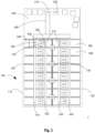
- a driver chip 1 comprises a first component area 100 and a second component area 200, each of which is rectangular, a lower edge of the first component area 100 is flush with a lower edge of the driver chip 1, a left edge of the first component area 100 is flush with a left edge of the driver chip 1, a right edge of the first component area 100 is flush with a right edge of the driver chip 1, the second component area 200 is located above the first component area 100, an upper edge of the second component area 200 is flush with an upper edge of the driver chip 1, a left edge of the second component area 200 is flush with the left edge of the driver chip 1, and a right edge of the second component area 200 is flush with the right edge of the driver chip 1.
- the first component area 100 includes a first driving channel group 110 and a second driving channel group 120, the first driving channel group 110 and the second driving channel group 120 are symmetrically distributed with each other with respect to a symmetrical axis, the first driving channel group 110 and the second driving channel group 120 each includes a same number of driving channels 300.
- the first driving channel group 110 includes eight driving channels 300
- the second driving channel group 120 also includes eight driving channels 300, and the driving channels 300 in the first driving channel group 110 and the driving channels 300 in the second driving channel group 120 are left-right symmetrically distributed.
- the first driving channel group and the second driving channel group may contain more or fewer driving channels and the above eight driving channels are only taken as a specific example and should not be taken for limitation.
- the second component area 200 is provided with an analog ground pad 210 (AVSS PAD) connected to a substrate 150 of the driving channels 300 in the first component area 100 through a metal wire 400.
- the substrate 150 is a P-type substrate.
- the second component area 200 is further provided with an analog power supply pad 220 (AVDD PAD), and optionally, both of the analog ground pad 210 and the analog power supply pad 220 are disposed close to the upper edge of the second component area 200 near the symmetry axis between the first driving channel group 110 and the second driving channel group 120.
- the metal wire 400 comprises an even number of metal lines which are symmetrically distributed.
- Fig. 2 shows a schematic diagram of an LED driver circuit according to an embodiment of the present application.
- the driver chip 1 includes a first component area 100 and a second component area 200.
- the first component area 100 includes a first driving channel group 110 and a second driving channel group 120, which are symmetrically arranged, and respectively include a same number of driving channels 300.
- Each of the driving channels 300 includes: a common-source device module 310, a common-gate device module 320, an electrostatic protection module 330, an operational amplifier module 340, and a blanking module 350, wherein in each of the driving channels 300, the common-source device module 310 is disposed on the driver chip 1 near the symmetry axis between the first driving channel group 110 and the second driving channel group 120, the common-gate device module 320 is adjacent to the common-source device module 310, the electrostatic protection module 330 is adjacent to the common-gate device module 320, the operational amplifier module 340 is adjacent to the electrostatic protection module 330, the blanking module 350 is adjacent to the operational amplifier module 340, and the blanking module 350 is disposed at an edge of the driver chip 1.
- the common-source device module 310 is disposed near the symmetry axis between the first driving channel group 110 and the second driving channel group 120, and the common-source device modules 310 in the driving channels of the first driving channel group 110 are adjacent to the common-source device modules 310 in the driving channels of the second driving channel group 120.
- the common-source device module 310 may be disposed at a middle position of the driver chip 1.
- the common-source device module 310, the common-gate device module 320, the electrostatic protection module 330, the operational amplifier module 340, and the blanking module 350 of each driving channel 300 are sequentially arranged from right to left; and in the second driving channel group 120, the common-source device module 310, the common-gate device module 320, the electrostatic protection module 330, the operational amplifier module 340, and the blanking module 350 of each driving channel 300 are sequentially arranged from left to right.
- all the driving channels 300 are arranged together, and the common-source device modules 310 which have the greatest influence on mismatch in the driving channels 300 are placed at the middle position of the driver chip 1, so that device mismatch can be effectively reduced, output current matching accuracy among the driving channels 300 can be improved, and good current consistency can be obtained.
- the first component area 100 further includes a plurality of output pads 130 (OUT PAD), which correspond to the driving channels 300, respectively, and are each disposed adjacent to the common-gate device module 320 and the electrostatic protection module 330 of a corresponding one of the driving channels 300.
- OUT PAD output pads 130
- the first driving channel group 110 and the second driving channel group 120 each include 8 driving channels 300
- the first component area 100 may include 16 output pads 130.
- the first component area 100 further includes a plurality of power ground pads 140 (OVSS PAD), each of which corresponds to four driving channels 300, and the power ground pads 140 are disposed on the symmetry axis between the first driving channel group 110 and the second driving channel group 120.
- the first driving channel group 110 and the second driving channel group 120 may each include 8 driving channels 300, and the first component area 100 may include 4 power ground pads 140 accordingly.
- the analog ground pad 210 of the second component area 200 is connected to the substrate 150 of the driving channels 300 in the first component area 100 through a metal wire 400.
- the metal wire 400 includes a first metal line 410, a second metal line 420, a third metal line 430, and a fourth metal wire 440, wherein the first metal line 410 is arranged on a left side of the output pads 130 of the first driving channel group 110, the second metal line 420 is arranged between the power ground pads 140 and the output pads 130 of the first driving channel group 110, the first metal line 410 and the second metal line 420 are used to connect to the substrate 150 of the second driving channel group 120, the third metal line 430 is arranged between the power ground pads 140 and the output pads 130 of the second driving channel group 120, the fourth metal line 440 is arranged on a right side of the output pads 130 of the second driving channel group 120, and the third metal line 430 and the fourth metal line 440 are used to connect to the substrate 150 of the second driving channel group 120.
- an operating current of each driving channel 300 is generally several milliamperes to tens of milliamperes.
- the substrate 150 of the driving channels 300 may be connected to the power supply pads 140, and a current source in each driving channel 300 may be continuously switched on and off under control of display data, which will cause significant noise on the power supply pads 140, resulting in high noise on a substrate voltage potential of the whole driver chip 1, thus affecting performance of a commonly used analog part of the second component area 200.
- internal noise is also one of the reasons for device mismatch.
- the analog ground pad 210 of the second component area 200 is connected to the substrate 150 of each driving channel 300 through the metal wire 400, and the metal wire 400 directly applies a ground voltage potential to a contact part of the substrate 150 of the first component area 100, thus effectively reducing internal noise of the driver chip 1.
- a layout structure of the driver chip 1 may be applicable to a LED display driver product with common-anode structure, and may also be applicable to a LED display driver product with common-cathode structure.
- the common-source device module 310 includes a first field effect transistor 311
- the common-gate device module 320 includes a second field effect transistor 321
- the operational amplifier module 340 includes an amplifier 341.
- the electrostatic protection module 330 includes an electro-static discharge (ESD) device.
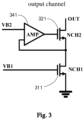
- Fig. 3 shows a schematic diagram of a constant current source circuit in a driving channel 300 according to an embodiment of the present application.
- the constant current source includes a first field effect transistor 311, a second field effect transistor 321 and an amplifier 341.
- Each of the first field effect transistor 311 and the second field effect transistor 321 is an NMOS (N-Metal-Oxide-Semiconductor) transistor.
- a source of the first field effect transistor 311 is grounded, a gate of the first field effect transistor 311 is connected to a first voltage input terminal, a drain of the first field effect transistor 311 is connected to a source of the second field effect transistor 321, a drain of the second field effect transistor 321 is connected to a circuit output terminal, a gate of the second field effect transistor 321 is connected to an output terminal of the amplifier 341, a first input terminal of the amplifier 341 is connected to a second voltage input terminal, and a second input terminal of the amplifier 341 is connected to the source of the second field effect transistor 321.
- constant driving current may be provided by a constant current source driver chip based on a PWM (Pulse Width Modulation) signal, and display grayscale of the LED display apparatus may be equal to the number of grayscale clock GCLK included in the PWM signal, so accuracy of a driving current of each driving channel will affect final display effect.
- PWM Pulse Width Modulation
- current accuracy mainly depends on an offset voltage of the first field effect transistor 311 and an offset voltage of the amplifier 341.
- an embodiment of the present application also provides an LED display apparatus, which comprises the LED driver circuit according to embodiments of the present disclosure, and the LED display apparatus can be, for example, an LED display screen, and can also be applied to any electronic equipment required to equip with an LED display screen.
- the technical proposal provided according to embodiments of the present disclosure can reduce internal noise of the chip, improve output current matching accuracy among the driving channels, thereby obtaining good current consistency and better ensuring the display effect of the LED display screen.
Landscapes
- Engineering & Computer Science (AREA)
- Physics & Mathematics (AREA)
- Computer Hardware Design (AREA)
- General Physics & Mathematics (AREA)
- Theoretical Computer Science (AREA)
- Control Of Indicators Other Than Cathode Ray Tubes (AREA)
- Devices For Indicating Variable Information By Combining Individual Elements (AREA)
- Led Devices (AREA)
Applications Claiming Priority (2)
| Application Number | Priority Date | Filing Date | Title |
|---|---|---|---|
| CN202011502630.0A CN112466249A (zh) | 2020-12-17 | 2020-12-17 | 一种led驱动电路 |
| PCT/CN2021/130740 WO2022127469A1 (fr) | 2020-12-17 | 2021-11-15 | Circuit de commande de del et appareil d'affichage à del |
Publications (2)
| Publication Number | Publication Date |
|---|---|
| EP4266301A1 true EP4266301A1 (fr) | 2023-10-25 |
| EP4266301A4 EP4266301A4 (fr) | 2024-11-20 |
Family
ID=74803897
Family Applications (1)
| Application Number | Title | Priority Date | Filing Date |
|---|---|---|---|
| EP21905398.0A Pending EP4266301A4 (fr) | 2020-12-17 | 2021-11-15 | Circuit de commande de del et appareil d'affichage à del |
Country Status (6)
| Country | Link |
|---|---|
| US (1) | US12444344B2 (fr) |
| EP (1) | EP4266301A4 (fr) |
| JP (1) | JP7725593B2 (fr) |
| KR (1) | KR102859084B1 (fr) |
| CN (1) | CN112466249A (fr) |
| WO (1) | WO2022127469A1 (fr) |
Families Citing this family (3)
| Publication number | Priority date | Publication date | Assignee | Title |
|---|---|---|---|---|
| CN112466249A (zh) | 2020-12-17 | 2021-03-09 | 北京集创北方科技股份有限公司 | 一种led驱动电路 |
| TWI824669B (zh) * | 2022-08-17 | 2023-12-01 | 大陸商北京集創北方科技股份有限公司 | Led驅動晶片通道佈局結構、led驅動晶片及顯示裝置 |
| TW202425712A (zh) * | 2022-12-07 | 2024-06-16 | 南韓商Lx半導體科技有限公司 | 用於靜電放電的電流源裝置以及包括該電流源裝置的顯示裝置 |
Family Cites Families (29)
| Publication number | Priority date | Publication date | Assignee | Title |
|---|---|---|---|---|
| JP3235614B2 (ja) * | 1990-04-24 | 2001-12-04 | セイコーエプソン株式会社 | 半導体チップの実装体とそれを用いた表示装置 |
| US5859392A (en) * | 1996-02-09 | 1999-01-12 | Lsi Logic Corporation | Method and apparatus for reducing noise in an electrostatic digitizing tablet |
| JP4043012B2 (ja) * | 2001-12-20 | 2008-02-06 | オプトレックス株式会社 | 表示素子の駆動回路と駆動方法 |
| DE10343278B4 (de) * | 2003-09-18 | 2006-01-05 | Infineon Technologies Ag | Halbbrückenschaltung mit einer Einrichtung zur Vermeidung von Querströmen |
| JP4010335B2 (ja) * | 2005-06-30 | 2007-11-21 | セイコーエプソン株式会社 | 集積回路装置及び電子機器 |
| KR101177577B1 (ko) * | 2005-12-30 | 2012-08-27 | 엘지디스플레이 주식회사 | 액정표시장치 |
| US8045944B2 (en) * | 2007-09-14 | 2011-10-25 | Qualcomm Incorporated | Offset correction for passive mixers |
| WO2009124432A1 (fr) * | 2008-04-11 | 2009-10-15 | 深圳市联德合微电子有限公司 | Circuit de commande de led à courant constant |
| CN100555617C (zh) * | 2008-05-04 | 2009-10-28 | 北京巨数数字技术开发有限公司 | 一种led的驱动芯片 |
| US8303694B2 (en) | 2008-05-27 | 2012-11-06 | Perkinelmer Health Sciences, Inc. | Chromatography systems and methods using them |
| KR100998729B1 (ko) * | 2008-11-13 | 2010-12-07 | 신무현 | 엘이디 구동 회로 |
| JP5519182B2 (ja) * | 2009-05-15 | 2014-06-11 | ルネサスエレクトロニクス株式会社 | 画像表示装置 |
| US8247992B2 (en) * | 2010-03-23 | 2012-08-21 | Green Mark Technology Inc. | LED driver circuit |
| CN102592542B (zh) * | 2012-02-27 | 2015-03-18 | 深圳市明微电子股份有限公司 | 一种led显示屏消隐控制电路及led驱动芯片 |
| CN102711323B (zh) * | 2012-05-09 | 2015-11-25 | 江苏应能微电子有限公司 | Led灯驱动电路 |
| JP6225511B2 (ja) * | 2013-07-02 | 2017-11-08 | セイコーエプソン株式会社 | 表示装置及び電子機器 |
| US9651632B1 (en) * | 2013-08-20 | 2017-05-16 | Ketra, Inc. | Illumination device and temperature calibration method |
| US9058762B2 (en) * | 2013-11-18 | 2015-06-16 | Sct Technology, Ltd. | Apparatus and method for driving LED display |
| CN104050924B (zh) * | 2014-06-27 | 2016-10-12 | 杭州士兰微电子股份有限公司 | Led驱动芯片及其控制方法和led模组 |
| CN204335010U (zh) * | 2014-12-23 | 2015-05-13 | 深圳市蓝丝腾科技有限公司 | 一种新型led恒流驱动电路 |
| US20170039957A1 (en) * | 2015-08-03 | 2017-02-09 | Solum Co., Ltd. | Led driver and display device for using the same |
| US9830416B2 (en) * | 2016-01-20 | 2017-11-28 | Anaglobe Technology, Inc. | Method for analog circuit placement |
| CN107342284A (zh) * | 2017-08-14 | 2017-11-10 | 武汉天马微电子有限公司 | 显示基板及显示装置 |
| CN108519707B (zh) * | 2018-03-29 | 2022-06-21 | 上海中航光电子有限公司 | 一种阵列基板及显示装置 |
| CN108650744B (zh) * | 2018-06-27 | 2024-05-03 | 北京集创北方科技股份有限公司 | Led驱动控制器、led驱动电路及led发光装置 |
| WO2020054096A1 (fr) * | 2018-09-11 | 2020-03-19 | ローム株式会社 | Dispositif de commande de del, dispositif d'éclairage et dispositif d'affichage embarqué |
| CN111369932B (zh) * | 2018-12-24 | 2023-03-17 | 北京新岸线移动多媒体技术有限公司 | 一种显示设备的驱动方法和驱动电路 |
| CN112466249A (zh) * | 2020-12-17 | 2021-03-09 | 北京集创北方科技股份有限公司 | 一种led驱动电路 |
| CN214012481U (zh) * | 2020-12-17 | 2021-08-20 | 北京集创北方科技股份有限公司 | 一种led驱动电路 |
-
2020
- 2020-12-17 CN CN202011502630.0A patent/CN112466249A/zh active Pending
-
2021
- 2021-11-15 US US18/268,304 patent/US12444344B2/en active Active
- 2021-11-15 KR KR1020237006753A patent/KR102859084B1/ko active Active
- 2021-11-15 JP JP2023537205A patent/JP7725593B2/ja active Active
- 2021-11-15 WO PCT/CN2021/130740 patent/WO2022127469A1/fr not_active Ceased
- 2021-11-15 EP EP21905398.0A patent/EP4266301A4/fr active Pending
Also Published As
| Publication number | Publication date |
|---|---|
| WO2022127469A1 (fr) | 2022-06-23 |
| CN112466249A (zh) | 2021-03-09 |
| EP4266301A4 (fr) | 2024-11-20 |
| KR102859084B1 (ko) | 2025-09-12 |
| JP2024500419A (ja) | 2024-01-09 |
| KR20230043190A (ko) | 2023-03-30 |
| US20240038146A1 (en) | 2024-02-01 |
| JP7725593B2 (ja) | 2025-08-19 |
| US12444344B2 (en) | 2025-10-14 |
Similar Documents
| Publication | Publication Date | Title |
|---|---|---|
| US12444344B2 (en) | LED driver circuit and LED display apparatus | |
| US11514845B2 (en) | Light-emitting diode display panel and light-emitting diode display device | |
| US10726774B2 (en) | Backlight driving circuit and method, backlight module, backlight circuit and display device | |
| EP3561801B1 (fr) | Panneau d'affichage | |
| CN107871454A (zh) | 微发光二极管显示面板 | |
| US20090295773A1 (en) | Display device | |
| US12211453B2 (en) | Driver circuit, driving method of the driver circuit, array substrate, and display device | |
| EP2927898A1 (fr) | Dispositif d'affichage à del et système de commande de del | |
| US11830862B2 (en) | Chip structure of micro light-emitting diode display | |
| TW202011629A (zh) | 微發光二極體顯示面板 | |
| CN116403514A (zh) | 用于发光二极管显示屏的驱动电路及其发光二极管显示屏 | |
| CN211929025U (zh) | Led显示装置及输出模块 | |
| GB2621953A (en) | Display panel and display device | |
| US11719974B2 (en) | Self-luminous body for display apparatus, self-luminous display apparatus, backlight, liquid crystal display apparatus, and method for manufacturing self-luminous body for display apparatus | |
| CN214012481U (zh) | 一种led驱动电路 | |
| KR102853013B1 (ko) | 백라이트 유닛 및 이를 포함하는 디스플레이 장치 | |
| CN114141819A (zh) | 显示装置 | |
| KR102853020B1 (ko) | 백라이트 유닛 및 이를 포함하는 디스플레이 장치 | |
| US20240212622A1 (en) | Display Substrate and Display Apparatus | |
| WO2022095549A1 (fr) | Plaque arrière d'excitation, panneau d'affichage et son procédé de préparation | |
| US20090213104A1 (en) | Source driver circuit | |
| US12444349B2 (en) | Display device | |
| US12061395B2 (en) | Flat lighting device and display device using light-emitting diode | |
| KR20220094324A (ko) | 디스플레이 장치 | |
| TWI641108B (zh) | 微發光二極體顯示面板 |
Legal Events
| Date | Code | Title | Description |
|---|---|---|---|
| STAA | Information on the status of an ep patent application or granted ep patent |
Free format text: STATUS: THE INTERNATIONAL PUBLICATION HAS BEEN MADE |
|
| PUAI | Public reference made under article 153(3) epc to a published international application that has entered the european phase |
Free format text: ORIGINAL CODE: 0009012 |
|
| STAA | Information on the status of an ep patent application or granted ep patent |
Free format text: STATUS: REQUEST FOR EXAMINATION WAS MADE |
|
| 17P | Request for examination filed |
Effective date: 20230717 |
|
| AK | Designated contracting states |
Kind code of ref document: A1 Designated state(s): AL AT BE BG CH CY CZ DE DK EE ES FI FR GB GR HR HU IE IS IT LI LT LU LV MC MK MT NL NO PL PT RO RS SE SI SK SM TR |
|
| DAV | Request for validation of the european patent (deleted) | ||
| DAX | Request for extension of the european patent (deleted) | ||
| A4 | Supplementary search report drawn up and despatched |
Effective date: 20241016 |
|
| RIC1 | Information provided on ipc code assigned before grant |
Ipc: G09G 3/32 20160101AFI20241011BHEP |