EP4167307B1 - Zinkoxid-nanomaterial und verfahren zu seiner herstellung sowie halbleiterbauelement - Google Patents
Zinkoxid-nanomaterial und verfahren zu seiner herstellung sowie halbleiterbauelement Download PDFInfo
- Publication number
- EP4167307B1 EP4167307B1 EP20941172.7A EP20941172A EP4167307B1 EP 4167307 B1 EP4167307 B1 EP 4167307B1 EP 20941172 A EP20941172 A EP 20941172A EP 4167307 B1 EP4167307 B1 EP 4167307B1
- Authority
- EP
- European Patent Office
- Prior art keywords
- zno
- nanomaterial
- surface ligand
- nanoparticle
- methoxybenzamide
- Prior art date
- Legal status (The legal status is an assumption and is not a legal conclusion. Google has not performed a legal analysis and makes no representation as to the accuracy of the status listed.)
- Active
Links
Images

Classifications
-
- H—ELECTRICITY
- H10—SEMICONDUCTOR DEVICES; ELECTRIC SOLID-STATE DEVICES NOT OTHERWISE PROVIDED FOR
- H10K—ORGANIC ELECTRIC SOLID-STATE DEVICES
- H10K30/00—Organic devices sensitive to infrared radiation, light, electromagnetic radiation of shorter wavelength or corpuscular radiation
- H10K30/10—Organic devices sensitive to infrared radiation, light, electromagnetic radiation of shorter wavelength or corpuscular radiation comprising heterojunctions between organic semiconductors and inorganic semiconductors
- H10K30/15—Sensitised wide-bandgap semiconductor devices, e.g. dye-sensitised TiO2
- H10K30/152—Sensitised wide-bandgap semiconductor devices, e.g. dye-sensitised TiO2 the wide bandgap semiconductor comprising zinc oxide, e.g. ZnO
-
- B—PERFORMING OPERATIONS; TRANSPORTING
- B82—NANOTECHNOLOGY
- B82Y—SPECIFIC USES OR APPLICATIONS OF NANOSTRUCTURES; MEASUREMENT OR ANALYSIS OF NANOSTRUCTURES; MANUFACTURE OR TREATMENT OF NANOSTRUCTURES
- B82Y30/00—Nanotechnology for materials or surface science, e.g. nanocomposites
-
- C—CHEMISTRY; METALLURGY
- C01—INORGANIC CHEMISTRY
- C01G—COMPOUNDS CONTAINING METALS NOT COVERED BY SUBCLASSES C01D OR C01F
- C01G9/00—Compounds of zinc
- C01G9/02—Oxides; Hydroxides
-
- C—CHEMISTRY; METALLURGY
- C09—DYES; PAINTS; POLISHES; NATURAL RESINS; ADHESIVES; COMPOSITIONS NOT OTHERWISE PROVIDED FOR; APPLICATIONS OF MATERIALS NOT OTHERWISE PROVIDED FOR
- C09K—MATERIALS FOR MISCELLANEOUS APPLICATIONS, NOT PROVIDED FOR ELSEWHERE
- C09K11/00—Luminescent materials, e.g. electroluminescent or chemiluminescent
- C09K11/02—Use of particular materials as binders, particle coatings or suspension media therefor
- C09K11/025—Use of particular materials as binders, particle coatings or suspension media therefor non-luminescent particle coatings or suspension media
-
- C—CHEMISTRY; METALLURGY
- C09—DYES; PAINTS; POLISHES; NATURAL RESINS; ADHESIVES; COMPOSITIONS NOT OTHERWISE PROVIDED FOR; APPLICATIONS OF MATERIALS NOT OTHERWISE PROVIDED FOR
- C09K—MATERIALS FOR MISCELLANEOUS APPLICATIONS, NOT PROVIDED FOR ELSEWHERE
- C09K11/00—Luminescent materials, e.g. electroluminescent or chemiluminescent
- C09K11/06—Luminescent materials, e.g. electroluminescent or chemiluminescent containing organic luminescent materials
-
- H—ELECTRICITY
- H10—SEMICONDUCTOR DEVICES; ELECTRIC SOLID-STATE DEVICES NOT OTHERWISE PROVIDED FOR
- H10K—ORGANIC ELECTRIC SOLID-STATE DEVICES
- H10K50/00—Organic light-emitting devices
- H10K50/10—OLEDs or polymer light-emitting diodes [PLED]
- H10K50/11—OLEDs or polymer light-emitting diodes [PLED] characterised by the electroluminescent [EL] layers
- H10K50/115—OLEDs or polymer light-emitting diodes [PLED] characterised by the electroluminescent [EL] layers comprising active inorganic nanostructures, e.g. luminescent quantum dots
-
- H—ELECTRICITY
- H10—SEMICONDUCTOR DEVICES; ELECTRIC SOLID-STATE DEVICES NOT OTHERWISE PROVIDED FOR
- H10K—ORGANIC ELECTRIC SOLID-STATE DEVICES
- H10K50/00—Organic light-emitting devices
- H10K50/10—OLEDs or polymer light-emitting diodes [PLED]
- H10K50/14—Carrier transporting layers
- H10K50/15—Hole transporting layers
-
- C—CHEMISTRY; METALLURGY
- C09—DYES; PAINTS; POLISHES; NATURAL RESINS; ADHESIVES; COMPOSITIONS NOT OTHERWISE PROVIDED FOR; APPLICATIONS OF MATERIALS NOT OTHERWISE PROVIDED FOR
- C09K—MATERIALS FOR MISCELLANEOUS APPLICATIONS, NOT PROVIDED FOR ELSEWHERE
- C09K11/00—Luminescent materials, e.g. electroluminescent or chemiluminescent
- C09K11/08—Luminescent materials, e.g. electroluminescent or chemiluminescent containing inorganic luminescent materials
- C09K11/56—Luminescent materials, e.g. electroluminescent or chemiluminescent containing inorganic luminescent materials containing sulfur
- C09K11/562—Chalcogenides
- C09K11/565—Chalcogenides with zinc cadmium
-
- C—CHEMISTRY; METALLURGY
- C09—DYES; PAINTS; POLISHES; NATURAL RESINS; ADHESIVES; COMPOSITIONS NOT OTHERWISE PROVIDED FOR; APPLICATIONS OF MATERIALS NOT OTHERWISE PROVIDED FOR
- C09K—MATERIALS FOR MISCELLANEOUS APPLICATIONS, NOT PROVIDED FOR ELSEWHERE
- C09K11/00—Luminescent materials, e.g. electroluminescent or chemiluminescent
- C09K11/08—Luminescent materials, e.g. electroluminescent or chemiluminescent containing inorganic luminescent materials
- C09K11/88—Luminescent materials, e.g. electroluminescent or chemiluminescent containing inorganic luminescent materials containing selenium, tellurium or unspecified chalcogen elements
- C09K11/881—Chalcogenides
- C09K11/883—Chalcogenides with zinc or cadmium
-
- C—CHEMISTRY; METALLURGY
- C09—DYES; PAINTS; POLISHES; NATURAL RESINS; ADHESIVES; COMPOSITIONS NOT OTHERWISE PROVIDED FOR; APPLICATIONS OF MATERIALS NOT OTHERWISE PROVIDED FOR
- C09K—MATERIALS FOR MISCELLANEOUS APPLICATIONS, NOT PROVIDED FOR ELSEWHERE
- C09K2211/00—Chemical nature of organic luminescent or tenebrescent compounds
- C09K2211/18—Metal complexes
- C09K2211/188—Metal complexes of other metals not provided for in one of the previous groups
-
- H—ELECTRICITY
- H10—SEMICONDUCTOR DEVICES; ELECTRIC SOLID-STATE DEVICES NOT OTHERWISE PROVIDED FOR
- H10K—ORGANIC ELECTRIC SOLID-STATE DEVICES
- H10K2102/00—Constructional details relating to the organic devices covered by this subclass
-
- H—ELECTRICITY
- H10—SEMICONDUCTOR DEVICES; ELECTRIC SOLID-STATE DEVICES NOT OTHERWISE PROVIDED FOR
- H10K—ORGANIC ELECTRIC SOLID-STATE DEVICES
- H10K30/00—Organic devices sensitive to infrared radiation, light, electromagnetic radiation of shorter wavelength or corpuscular radiation
- H10K30/50—Photovoltaic [PV] devices
-
- H—ELECTRICITY
- H10—SEMICONDUCTOR DEVICES; ELECTRIC SOLID-STATE DEVICES NOT OTHERWISE PROVIDED FOR
- H10K—ORGANIC ELECTRIC SOLID-STATE DEVICES
- H10K50/00—Organic light-emitting devices
- H10K50/10—OLEDs or polymer light-emitting diodes [PLED]
- H10K50/14—Carrier transporting layers
- H10K50/16—Electron transporting layers
-
- H—ELECTRICITY
- H10—SEMICONDUCTOR DEVICES; ELECTRIC SOLID-STATE DEVICES NOT OTHERWISE PROVIDED FOR
- H10K—ORGANIC ELECTRIC SOLID-STATE DEVICES
- H10K85/00—Organic materials used in the body or electrodes of devices covered by this subclass
- H10K85/10—Organic polymers or oligomers
- H10K85/111—Organic polymers or oligomers comprising aromatic, heteroaromatic, or aryl chains, e.g. polyaniline, polyphenylene or polyphenylene vinylene
- H10K85/115—Polyfluorene; Derivatives thereof
-
- H—ELECTRICITY
- H10—SEMICONDUCTOR DEVICES; ELECTRIC SOLID-STATE DEVICES NOT OTHERWISE PROVIDED FOR
- H10K—ORGANIC ELECTRIC SOLID-STATE DEVICES
- H10K85/00—Organic materials used in the body or electrodes of devices covered by this subclass
- H10K85/10—Organic polymers or oligomers
- H10K85/141—Organic polymers or oligomers comprising aliphatic or olefinic chains, e.g. poly N-vinylcarbazol, PVC or PTFE
- H10K85/146—Organic polymers or oligomers comprising aliphatic or olefinic chains, e.g. poly N-vinylcarbazol, PVC or PTFE poly N-vinylcarbazol; Derivatives thereof
-
- H—ELECTRICITY
- H10—SEMICONDUCTOR DEVICES; ELECTRIC SOLID-STATE DEVICES NOT OTHERWISE PROVIDED FOR
- H10K—ORGANIC ELECTRIC SOLID-STATE DEVICES
- H10K85/00—Organic materials used in the body or electrodes of devices covered by this subclass
- H10K85/10—Organic polymers or oligomers
- H10K85/151—Copolymers
-
- H—ELECTRICITY
- H10—SEMICONDUCTOR DEVICES; ELECTRIC SOLID-STATE DEVICES NOT OTHERWISE PROVIDED FOR
- H10K—ORGANIC ELECTRIC SOLID-STATE DEVICES
- H10K85/00—Organic materials used in the body or electrodes of devices covered by this subclass
- H10K85/20—Carbon compounds, e.g. carbon nanotubes or fullerenes
- H10K85/211—Fullerenes, e.g. C60
-
- H—ELECTRICITY
- H10—SEMICONDUCTOR DEVICES; ELECTRIC SOLID-STATE DEVICES NOT OTHERWISE PROVIDED FOR
- H10K—ORGANIC ELECTRIC SOLID-STATE DEVICES
- H10K85/00—Organic materials used in the body or electrodes of devices covered by this subclass
- H10K85/30—Coordination compounds
- H10K85/381—Metal complexes comprising a group IIB metal element, e.g. comprising cadmium, mercury or zinc
Definitions
- the present disclosure generally relates to the display technology field and, more particularly, to a zinc oxide (ZnO) nanomaterial, a preparation method of the ZnO nanomaterial, and a semiconductor device.
- ZnO zinc oxide
- An electron transport layer material such as a zinc oxide (ZnO) based nanocrystal is widely studied to be used as a carrier transport material of a quantum dot light-emitting diode (QLED) device.
- ZnO zinc oxide
- QLED quantum dot light-emitting diode
- a particle diameter of a ZnO nanoparticle used for forming a nano ZnO electron transport layer is generally close to or even less than 5 nm, the ZnO nanoparticle has a very large specific surface area, which causes the ZnO particle to be very unstable to easily result in agglomeration.
- the agglomeration of ZnO particles has a great impact on film formation and electron transport performance.
- surface ligands may be introduced on surfaces of the ZnO nanoparticles.
- the surface ligands increase a transport distance of the electron in the nano ZnO electron transport layer after the film is formed, thereby hindering the transport of the electrons in the ZnO material.
- the conductivity of the nano ZnO electron transport layer may be affected.
- a surface defect of the ZnO as a nonradiative recombination center may generate an obvious quenching effect on excitons to greatly reduce the light-emitting efficiency of the quantum dot.
- One of the objectives of embodiments of the present disclosure is to provide a zinc oxide (ZnO) nanomaterial, a preparation method thereof, and a semiconductor device having the ZnO nanomaterial, and aims to solve the problem that the surface ligand of the ZnO nanoparticle increases the electronic transition distance of nano ZnO thin films to block the electrons transport of in the ZnO material.
- ZnO zinc oxide
- a technical solution adopted by embodiments of the present disclosure includes as follows.
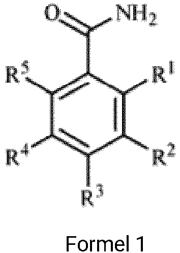
- a zinc oxide (ZnO) nanomaterial including a ZnO nanoparticle and a surface ligand bonded to the ZnO nanoparticle, and the surface ligand having a structure as shown in Formula 1 wherein in Formula 1, R 1 , R 2 , R 3 , R 4 , and R 5 each includes at least one of hydrogen, alkoxy group with a carbon number of one to three, or amino group, and R 1 , R 2 , R 3 , R 4 , and R 5 include one to three alkoxy groups with a carbon number of one to three and zero to one amino group.
- a preparation method of a ZnO nanomaterial includes preparing a mixed solution of a ZnO nanoparticle and a surface ligand, wherein the surface ligand has a structure as shown in Formula 1 in Formula 1, R 1 , R 2 , R 3 , R 4 , and R 5 each includes at least one of hydrogen, alkoxy group with a carbon number of one to three, or amino group, and R 1 , R 2 , R 3 , R 4 , and R 5 include one to three alkoxy groups with a carbon number of one to three and zero to one amino group; and causing the ZnO nanoparticle to react with the surface ligand in the mixed solution to prepare ZnO nanoparticle having the surface ligand bonded thereto
- a semiconductor device in a third aspect, includes an anode and a cathode arranged oppositely to each other, an active layer arranged between the anode and the cathode, and an electron transport layer arranged between the active layer and the cathode, wherein the material of the electron transport layer includes a ZnO nanomaterial, the ZnO nanomaterial includes a ZnO nanoparticle and a surface ligand bonded to a surface of the ZnO nanoparticle, the surface ligand has a structure as shown in Formula 1 in Formula 1, R 1 , R 2 , R 3 , R 4 , and R 5 each includes at least one of hydrogen, alkoxy group with a carbon number of one to three, or amino group, and R 1 , R 2 , R 3 , R 4 , and R 5 include one to three alkoxy groups with a carbon number of one to three and zero to one amino group.
- the nanomaterial is used as the electron transport layer. Therefore, the obtained semiconductor device has good photoelectric efficiency and stability.
- a first aspect of embodiments of the present disclosure provides a zinc oxide (ZnO) nanomaterial.
- the ZnO nanomaterial may include a ZnO nanoparticle and a surface ligand bonded to the ZnO nanoparticle.
- a structure of the surface ligand is shown in Formula 1 below.
- R 1 , R 2 , R 3 , R 4 , and R 5 may each independently be at least one selected from, e.g., hydrogen, an alkoxy group with a carbon number of one to three, and amino group, and amino group.
- R 1 , R 2 , R 3 , R 4 , and R 5 may include one to three alkoxy groups with a carbon number of one to three and zero to one amino group.
- the ZnO nanomaterial of embodiments of the present disclosure may include the ZnO nanoparticle and the surface ligand of an alkoxyphenylamide structure shown in Formula 1 that is bonded to the ZnO nanoparticle. Since the ligand is absorbed on the surface of the ZnO nanoparticle, a distance between ZnO nanoparticles may be increased, and surface contact may be reduced to reduce the agglomeration.
- an oxygen void bond in the alkoxy group may be combined with a suspended Zn bond in the ZnO nanoparticle to passivate the surface defect of the ZnO nanoparticle, reduce the quenching effect on the exciton by the surface defect of the ZnO as the nonradiative recombination center, and improve the recombination capability of the carriers.
- the alkoxyphenylamide structure may have a conjugated ⁇ bond, which may effectively improve transport ability of the carrier and the conductivity of the ZnO nanomaterial.
- the movement of the carrier may be enhanced, and the transport ability of the carrier may be improved, when the ZnO nanoparticle is used as the functional layer material of the semiconductor device.
- the agglomeration may be reduced, and the conductivity may be improved.
- the alkoxy group with a carbon number of one to three may provide a bonding point for bonding the surface ligand with the ZnO nanoparticle.
- using a phenylamide structure as the surface ligand may increase the electron transition distance between the ZnO nanoparticles. Since the benzamide in the alkoxyphenylamide structure has a conjugated ⁇ bond, the transport ability of the ZnO nanoparticle on the carrier may be effectively improved, which can eliminate the impact on the conductivity of the ZnO nanomaterial due to the increase of the electron transition distance between the ZnO particles. Moreover, with the benzamide, the conductivity of the ZnO particle may be further enhanced.
- R 1 , R 2 , R 3 , R 4 , and R 5 may include two alkoxy groups with a carbon number of one to three and zero to one amino group, and at least R 2 or R 3 may be alkoxy group with a carbon number of one to three. That is, two of R 1 , R 2 , R 3 , R 4 , and R 5 may be alkoxy group with a carbon number of one to three, and zero to one of R 1 , R 2 , R 3 , R 4 , and R 5 is amino group. In this situation, a space steric hindrance of the alkoxyphenylamide structure may be small.
- the conductivity of the ZnO nanoparticle may be improved. If too many of R 1 , R 2 , R 3 , R 4 , and R 5 are substituent groups, such as more than 3 (greater than 3), the effect of increasing the electron transition distance between the ZnO particles caused by a phenylamide structure may be obvious, and the effect of improving the conductivity of the ZnO nanoparticle through the conjugated ⁇ bond of the benzamide may be reduced.
- the surface ligand may be at least one selected from, e.g., p-methoxybenzamide, m-methoxybenzamide, o-methoxybenzamide, p-ethoxybenzamide, m-ethoxybenzamide, o-ethoxybenzamide, 2,5-dimethoxybenzamide, 3,5-dimethoxybenzamide, 2,4-dimethoxybenzamide, 3,4-dimethoxybenzamide, or 5-amino-4-methoxybenzamide.
- the surface ligand may passivate the surface defect of the ZnO nanoparticle, and may also have an efficient carrier transport and injection ability.
- the ZnO nanomaterial may include the ZnO nanoparticle and the surface ligand bonded to the ZnO nanoparticle.
- a molar ratio of the ZnO nanoparticle to the surface ligand bonded to the ZnO nanoparticle may range from 1:5 to 1:50.
- the molar ratio of the ZnO nanoparticle to the surface ligand bonded to the ZnO nanoparticle may be within the above range.
- the surface ligand may be fully combined with the reaction points on the ZnO nanoparticle to improve the surface defect of the ZnO nanoparticle and improve the electron transport performance of the ZnO nanoparticle.
- the combination of the surface ligand to the ZnO nanoparticle may not be strong enough, and hence the surface ligand may easily fall off, affecting the electron transport performance of the nanomaterial.
- the surface ligand bonded to the ZnO nanoparticle When the molar content of the surface ligand bonded to the ZnO nanoparticle is too low, for example, when the molar content of the ZnO nanoparticle is 1 and the molar content of the surface ligand is less than 5, the surface ligand may have a limited effect on the ZnO nanoparticle electron transport layer, which is insufficient to achieve a significant improvement.
- the nanomaterial of embodiments of the present disclosure may be prepared by the following method.
- a second aspect of embodiments of the present disclosure provide a preparation method of a ZnO nanomaterial.
- the method includes the following processes.
- a mixed solution of the ZnO nanoparticle and the surface ligand is prepared, wherein the structure of the surface ligand is shown in Formula 1 below.
- R 1 , R 2 , R 3 , R 4 , and R 5 may each independently be at least one selected from, e.g., hydrogen, an alkoxy group with a carbon number of one to three, and amino group.
- R 1 , R 2 , R 3 , R 4 , and R 5 may include one to three alkoxy groups with a carbon number of one to three and zero to one amino group.
- the ZnO nanoparticle reacts with the surface ligand to prepare the ZnO nanoparticle having the surface ligand.
- the preparation method of the ZnO nanomaterial of embodiments of the present disclosure only the mixed solution of the ZnO nanoparticle and the surface ligand may need to be prepared.
- the surface ligand may be bonded to the surface of the ZnO nanoparticle.
- the process of the method may be simple, and the condition of the method may be mild. The method may be easily used to realize large-scale production.
- the dispersity and conductivity of the ZnO nanomaterial may be improved.
- the ZnO nanoparticle and the surface ligand may be used as raw materials for preparing the ZnO nanomaterial.
- the structure of the surface ligand may be the one shown in Formula 1.
- R 1 , R 2 , R 3 , R 4 , and R 5 may include two alkoxy groups with a carbon number of one to three and zero to one amino group, and at least R 2 or R 3 may be an alkoxy group with a carbon number of one to three.
- the surface ligand may be at least one selected from, e.g., p-methoxybenzamide, m-methoxybenzamide, o-methoxybenzamide, p-ethoxybenzamide, m-ethoxybenzamide, o-ethoxybenzamide, 2,5-dimethoxybenzamide, 3,5-dimethoxybenzamide, 2,4-dimethoxybenzamide, 3,4-dimethoxybenzamide, or 5-amino-4-methoxybenzamide.
- the ZnO nanoparticle may be prepared by the method below.
- a preparation method of a ZnO nanoparticle includes:
- the zinc salt may be selected from an inorganic zinc salt and/or an organic zinc salt capable of ionizing to generate a zinc ion.
- the zinc salt may be at least one selected from, but is not limited to, e.g., zinc acetate, zinc nitrate, zinc chloride, zinc sulfate, or zinc acetate dihydrate.
- the alkali source may be at least one selected from, e.g., inorganic alkali and/or organic alkali that can generate hydroxide ions in the mixed solution formed by adding the zinc salt organic solution into the alkali solution.
- the alkali source may include, but is not limited to, at least one of sodium hydroxide, potassium hydroxide, lithium hydroxide, or pentahydrate tetramethylammonium hydroxide.
- the zinc salt may be dissolved in the organic solvent.
- the organic solvent may be organic alcohol, including but not limited to at least one of isopropanol, ethanol, propanol, butanol, pentanol, or hexanol.
- the alkali source is dissolved in the organic solvent for mixing.
- the organic solvent may be organic alcohol, including but not limited to at least one of isopropanol, ethanol, propanol, butanol, pentanol, or hexanol.
- the organic solvent for dissolving the alkali source may be the same as the organic solvent for dissolving the zinc salt.
- step S03 the organic solution of the zinc salt is added to the alkali solution for mixing with a molar ratio of Zn ions to OH - being 1:(1-2).
- the alkali solution may react with the organic solution of the zinc salt to generate the ZnO nanoparticle.
- the mixing process may adopt a stirring and mixing manner.
- preparing the mixed solution of the ZnO nanoparticle and the surface ligand may include preparing the organic solution of the ZnO particle first and then adding the surface ligand into the organic solution of the ZnO particle to form the mixed solution.
- the mixed solution may be formed by dispersing the ZnO particle and the surface ligand in the organic solution, or preparing the organic solution of the surface ligand first and then adding the ZnO particle to the organic solution of the surface ligand.
- the mixed solution may be formed by first preparing the organic solution of the ZnO nanoparticle and then adding the surface ligand into the organic solution of the ZnO nanoparticle.
- the mixed solution of the ZnO nanoparticle and the surface ligand may be prepared.
- the molar ratio of the ZnO nanoparticle to the surface ligand may range from 1:5 to 1:50.
- the reaction temperature may range from 20°C to 60° C.
- a third aspect of embodiments of the present disclosure provides a semiconductor device, including an anode and a cathode arranged oppositely to each other, an active layer arranged between the anode and the cathode, and an electron transport layer arranged between the active layer and the cathode, wherein a material of the electron transport layer includes the ZnO nanomaterial, the zinc oxide nanomaterial includes the ZnO nanoparticle and the surface ligand bonded to the ZnO nanoparticle, the structure of the surface ligand is shown in Formula 1 below in Formula 1, R 1 , R 2 , R 3 , R 4 , and R 5 may each independently be at least one selected from, e.g., hydrogen, an alkoxy group with a carbon number of one to three, and amino group, and R 1 , R 2 , R 3 , R 4 , and R 5 may include one to three alkoxy groups with a carbon number of one to three and zero to one amino group.
- the above nanomaterial may be used as the electron transport layer. Therefore, the obtained semiconductor device may have good photoelectric efficiency and stability.
- the ZnO nanomaterial may include the ZnO nanoparticle and the surface ligand shown in Formula 1 bonded to the ZnO nanoparticle.
- the alkoxy group with a carbon number of one to three may provide the bonding point for bonding the surface ligand with the ZnO nanoparticle.
- using the phenylamide structure as the surface ligand which may increase the electron transition distance between the zinc oxide nanoparticles.
- the transport ability of the ZnO nanoparticle on the carrier may be effectively improved, which can eliminate the impact on the conductivity of the ZnO nanomaterial due to the increase of the electron transition distance between the ZnO particles.
- the conductivity of the ZnO particle may be further enhanced.
- R 1 , R 2 , R 3 , R 4 , and R 5 may include two alkoxy groups with a carbon number of one to three and zero to one amino group, and at least R 2 or R 3 may be the alkoxy group with a carbon number of one to three.
- two of R 1 , R 2 , R 3 , R 4 , and R 5 may be thealkoxy group with a carbon number of one to three, and zero to one of R 1 , R 2 , R 3 , R 4 , and R 5 may be the amino group.
- a space steric hindrance of the alkoxyphenylamide structure may be small.
- the conductivity of the ZnO nanoparticle may be improved. If too many of R 1 , R 2 , R 3 , R 4 , and R 5 are substituent groups, such as more than 3 (greater than 3), the effect of increasing the electron transition distance between the ZnO particles caused by phenylamide structure may be obvious, and the effect of improving the conductivity of the ZnO nanoparticle through the conjugated ⁇ bond of the benzamide may be reduced.
- the surface ligand may be at least one selected from, e.g., p-methoxybenzamide, m-methoxybenzamide, o-methoxybenzamide, p-ethoxybenzamide, m-ethoxybenzamide, o-ethoxybenzamide, 2,5-dimethoxybenzamide, 3,5-dimethoxybenzamide, 2,5-dimethoxybenzamide, 3,4-dimethoxybenzamide, or 5-amino-4-methoxybenzamide.
- the surface ligand may passivate the surface defect of the ZnO nanoparticle, and may also have the efficient carrier transport and injection ability.
- the ZnO nanomaterial may include the ZnO nanoparticle and the surface ligand bonded to the ZnO nanoparticle.
- a molar ratio of the ZnO nanoparticle to the surface ligand bonded to the ZnO nanoparticle may range from 1:5 to 1:50.
- the molar ratio of the ZnO nanoparticle to the surface ligand bonded to the ZnO nanoparticle may be within the above range.
- the surface ligand may be fully combined with the reaction points on the ZnO nanoparticle to improve the surface defect of the ZnO nanoparticle and improve the electron transport performance of the ZnO nanoparticle.
- the combination of the surface ligand to the ZnO nanoparticle may not be strong enough, and hence the surface ligand may easily fall off, affecting the electron transport performance of the nanomaterial.
- the surface ligand bonded to the ZnO nanoparticle When the molar content of the surface ligand bonded to the ZnO nanoparticle is too low, for example, when the molar content of the ZnO nanoparticles is 1, and the molar content of the surface ligand is less than 5, the surface ligand may have the limited effect on the ZnO nanoparticle electron transport layer, which is insufficient to achieve a significant improvement.
- the thickness of the electron transport layer may range from 70 to 90 nm.
- the semiconductor device may include a solar cell (a device absorbs light through the active layer, such as a perovskite solar cell) or a light-emitting device (the device emits light from a top electrode or a bottom electrode, and the active layer is a light-emitting layer).
- the light-emitting device may include an organic light-emitting diode or a quantum dot light-emitting diode.
- the quantum dot light-emitting diode may include a perovskite light-emitting diode.
- the active layer may include the quantum dot light-emitting layer.
- the semiconductor device may include the quantum dot light-emitting diode.
- the light-emitting device of embodiments of the present disclosure may be divided into a forward structure electroluminescent device and an inverted structure electroluminescent device.
- the forward structure includes a substrate, an anode, a quantum dot light-emitting layer, an electron transport layer, and a cathode, optional hole functional layer(s), such as a hole injection layer, a hole transport layer, and/or an electron blocking layer, arranged between the anode and the quantum dot light-emitting layer, and an optional electron injection layer arranged between the electron transport layer and the cathode.
- the inverted structure is the opposite of the forward structure.
- the ZnO nanoparticle may be used as the electron transport layer of the QLED device.
- the amino group may be introduced on the surface ligand of the ZnO nanomaterial, which can enhance the coordination ability of the electron transport material and the ligand on the surface of the quantum dot.
- the movement of the carrier may be further enhanced, and the transport ability of the carrier may be improved.
- the anode may include a doped metal oxide, for example, an indium-doped tin oxide (ITO).
- ITO indium-doped tin oxide
- a material of the hole transport layer may be selected from poly (9,9-dioctylfluorenyl-2,7-diyl)-co-(4,4'-( N -(4-sec-butylphenyl)diphenylamine)] (TFB), polyvinylcarbazole (PVK) , etc.
- a material of the quantum dot light-emitting layer may be selected from CdS, CdSe, etc.
- a material of the cathode may be selected from one or more of a conductive carbon material (e.g., C60), a conductive metal oxide material (e.g., ITO), and a metal material (e.g., Ag).
- the light-emitting device may further include a packaging layer.
- the packaging layer may be arranged on a surface of the top electrode (the electrode away from the substrate) or a surface of the entire electroluminescent device.
- the quantum dot light-emitting diode may be prepared by the following method.
- a preparation method of a quantum dot light-emitting diode includes: Providing a substrate and depositing the ZnO nanomaterial on the substrate to form an electron transport layer.
- the ZnO nanomaterial may be deposited on the substrate by a chemical method or a physical method.
- the chemical method may include, but is not limited to, a chemical vapor deposition method or a continuous ion layer adsorption and reaction method.
- the physical method may include, but is not limited to, a physical coating method or a solution method.
- the ZnO nanomaterial may be formulated into a solution and the deposition of the ZnO nanomaterial can be realized using a solution processing method.
- the solution processing method may include, but is not limited to, spin coating, inkjet printing, etc.
- an annealing treatment may be performed to remove the solvent in the film layer to obtain the electron transport layer.
- remaining film layers may be formed on the electron transport layer.
- a cathode may be formed on the electron transport layer to obtain the quantum dot light-emitting diode.
- the quantum dot light-emitting layer and the anode may be formed on the electron transport layer in sequence to obtain the quantum dot light-emitting diode.
- the hole transport layer may be formed on the surface of the quantum dot light-emitting layer away from the electron transport layer.
- the layers in the quantum dot light-emitting diode may include the hole transport layer, the quantum dot light-emitting layer, the cathode, and the anode, which may be formed by a chemical method or a physical method.
- the chemical method may include, but is not limited to, a chemical vapor deposition method or an anode oxidation method.
- the physical method may include, but is not limited to, a physical coating method or a solution method.
- the preparation method may further include performing packaging processing on the obtained QLED device.
- the packaging processing may be performed by a common machine or manually.
- the oxygen content and the water content in the packaging processing environment may be less than 0.1 ppm to ensure the stability of the QLED device.
- a ZnO nanomaterial includes a ZnO nanoparticle and p-methoxybenzamide bonded to the ZnO nanoparticle.
- a preparation method of the ZnO nanomaterial includes the following steps.
- Zinc acetate with a proper amount is added to a 50 ml ethanol solution to prepare a zinc acetate ethanol solution of 1 mol/L.
- the solution is stirred and dissolved at 70 °C to obtain a first precursor solution.
- Potassium hydroxide is weighed according to a ratio of Zn atoms to OH-molar at 1:1.5.
- the potassium hydroxide is added to 50 ml of ethanol solution to prepare a 1.5 mol/L potassium hydroxide solution.
- the potassium hydroxide solution is stirred and dissolved to obtain a second precursor solution.
- the first precursor solution is injected into the second precursor solution.
- An injection rate is 10 ml/min, and magnetic stirring and mixing are performed for 30 min to prepare the ZnO nanoparticle.
- p-methoxybenzamide powder is added and heated to 50°C for magnetic stirring until the solution is completely clarified.
- the surface-modified ZnO nanomaterial is obtained after cleaning.
- a ZnO nanomaterial includes a ZnO nanoparticle and p-ethoxybenzamide bonded to the ZnO nanoparticle.
- a preparation method of the ZnO nanomaterial includes the following steps.
- Zinc nitrate with a proper amount is added to 50 ml of the propanol solution to prepare a zinc nitrate solution of 1 mol/L.
- the solution is stirred and dissolved at 70°C to obtain a first precursor solution.
- Sodium hydroxide is weighed according to a molar ratio of Zn atom to OH-at 1:1.3.
- the sodium hydroxide is added to 50 ml of propanol solution to prepare a sodium hydroxide solution of 1.3 mol/l.
- the sodium hydroxide solution is stirred and dissolved to obtain a second precursor solution.
- the first precursor solution is injected into the second precursor solution.
- An injection rate is 5 ml/min.
- Magnetic stirring and mixing are performed for 30 min to prepare the ZnO nanoparticle.
- p-ethoxybenzamide powder is added and heated to 50°C for magnetic stirring until the solution is completely clarified.
- the surface-modified ZnO nanomaterial is obtained after cleaning.
- a ZnO nanomaterial includes a ZnO nanoparticle and m-methoxybenzamide bonded to the ZnO nanoparticle.
- a preparation method of the ZnO nanomaterial includes the following steps.
- Zinc chloride with a proper amount is added to 50 ml of a butanol solution to prepare a zinc chloride butanol solution of 1 mol/L.
- the solution is stirred and dissolved at 70°C to obtain a first precursor solution.
- Potassium hydroxide is weighed according to a molar ratio of Zn atom to OH- at 1: 1.1.
- the potassium hydroxide is added to 50 ml of the propanol solution to prepare the potassium hydroxide solution of 1.1 mol/L.
- the potassium hydroxide solution is stirred and dissolved to obtain a second precursor solution.
- the first precursor solution is injected into the second precursor solution.
- An injection rate is 8 ml/min.
- the magnetic stirring and mixing are performed for 30 min to prepare the ZnO nanoparticle.
- m-methoxybenzamide powder is added and heated to 50°C for magnetic stirring until the solution is completely clarified.
- the surface-modified ZnO nanomaterial is obtained after cleaning.
- a preparation method of the ZnO nanomaterial includes the following steps.
- the first precursor solution is injected into the second precursor solution.
- the injection rate is 8 ml/min.
- the magnetic stirring and mixing are performed for 30 min to prepare the ZnO nanoparticle.
- the m-methoxybenzamide powder is added and heated to 50°C for magnetic stirring until the solution is completely clarified.
- the surface-modified ZnO nanomaterial is obtained after cleaning.
- Zinc acetate with a proper amount is added to a 50 ml ethanol solution to prepare a zinc acetate ethanol solution of 1 mol/L.
- the solution is stirred and dissolved at 70°C to obtain the first precursor solution.
- the potassium hydroxide is weighed according to a molar ratio of Zn atom to OH- at 1:1.1.
- the sodium hydroxide is added to a 50 ml ethanol solution to prepare a 1.1 mol/L potassium hydroxide solution.
- the potassium hydroxide solution is stirred and dissolved to obtain the second precursor solution.
- the first precursor solution is injected into the second precursor solution.
- the injection rate is 10 ml/min.
- the magnetic stirring and mixing are performed for 30 min to prepare the ZnO nanoparticle.
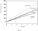
- a conductivity test is performed on the ZnO nanomaterials prepared in Examples 1-3 and Comparative Example 1.
- a test method is as follows.
- a device with a laminated structure such as ITO/ZnO/Al may be provided.
- a relationship between the current and the voltage is characterized.
- d denotes a thickness of a film layer
- A denotes a device area.
- the test results are shown in FIG. 5 .
- a relative current density of the ZnO nanomaterial modified by the alkoxyphenylamide structure of embodiments of the present disclosure is higher than a relative current density of the ZnO nanoparticle without being modified. Compared with the modified ZnO nanoparticle, the conductivity of the ZnO nanomaterial modified by the alkoxyphenylamide structure embodiments of the present disclosure may be enhanced.
Landscapes
- Chemical & Material Sciences (AREA)
- Engineering & Computer Science (AREA)
- Physics & Mathematics (AREA)
- Nanotechnology (AREA)
- Inorganic Chemistry (AREA)
- Materials Engineering (AREA)
- Organic Chemistry (AREA)
- Crystallography & Structural Chemistry (AREA)
- Optics & Photonics (AREA)
- Electromagnetism (AREA)
- Composite Materials (AREA)
- Condensed Matter Physics & Semiconductors (AREA)
- General Physics & Mathematics (AREA)
- Inorganic Compounds Of Heavy Metals (AREA)
Claims (15)
- Zinkoxid-Nanomaterial (ZnO), mit einem ZnO-Nanopartikel und einem Oberflächenliganden, der mit dem ZnO-Nanopartikel gebondet ist, wobei der Oberflächenligand eine Struktur wie in Formel 1 gezeigt aufweist:
- ZnO-Nanomaterial nach Anspruch 1, wobei R1, R2, R3, R4 und R5 zwei Alkoxygruppen mit einer Kohlenstoffzahl von eins bis drei und null bis eine Aminogruppe beinhalten, und wobei zumindest R2 oder R3 eine Alkoxygruppe mit einer Kohlenstoffzahl von eins bis drei ist.
- ZnO-Nanomaterial nach Anspruch 1 oder 2, wobei der Oberflächenligand zumindest eines von p-Methoxybenzamid, m-Methoxybenzamid, o-Methoxybenzamid, p-Ethoxybenzamid, m-Ethoxybenzamid, o-Ethoxybenzamid, 2,5-Dimethoxybenzamid, 3,5-Dimethoxybenzamid, 2,4-Dimethoxybenzamid, 3,4-Dimethoxybenzamid oder 5-Amino-4-Methoxybenzamid beinhaltet.
- ZnO-Nanomaterial nach Anspruch 3, wobei das ZnO-Nanomaterial aus dem ZnO-Nanopartikel und dem mit dem ZnO-Nanopartikel gebondeten Oberflächenliganden besteht.
- ZnO-Nanomaterial nach einem der Ansprüche 1, 2 und 4, wobei bei dem ZnO-Nanomaterial ein Molverhältnis des ZnO-Nanopartikels zu dem mit dem ZnO-Nanopartikel gebondeten Oberflächenliganden zwischen 1:5 und 1:50 liegt.
- Herstellungsverfahren eines Zinkoxid-Nanomaterials (ZnO), mit den Schritten:
Herstellen einer gemischten Lösung eines ZnO-Nanopartikels und eines Oberflächenliganden, wobei der Oberflächenligand eine Struktur wie in Formel 1 gezeigt aufweist: wobei R1, R2, R3, R4 und R5 jeweils zumindest eines von Wasserstoff, einer Alkoxygruppe mit einer Kohlenstoffzahl von eins bis drei, oder eine Aminogruppe beinhalten, und R1, R2, R3, R4 und R5 eine bis drei Alkoxygruppen mit einer Kohlenstoffzahl von eins bis drei und null bis eine Aminogruppe beinhalten; undVeranlassen, dass der ZnO-Nanopartikel mit dem Oberflächenliganden in der gemischten Lösung reagiert, um den ZnO-Nanopartikel mit dem damit gebondeten Oberflächenliganden herzustellen.
 - Herstellungsverfahren des ZnO-Nanomaterials nach Anspruch 6, wobei in Formel 1 R1, R2, R3, R4 und R5 zwei Alkoxygruppen mit einer Kohlenstoffzahl von eins bis drei und null bis eine Aminogruppe beinhalten, und zumindest R2 oder R3 eine Alkoxygruppe mit einer Kohlenstoffzahl von eins bis drei ist.
- Herstellungsverfahren des ZnO-Nanomaterials nach Anspruch 6, wobei der Oberflächenligand zumindest eines ist, das aus z.B. p-Methoxybenzamid, m-Methoxybenzamid, o-Methoxybenzamid, p-Ethoxybenzamid, m-Ethoxybenzamid, o-Ethoxybenzamid, 2,5-Dimethoxybenzamid, 3,5-Dimethoxybenzamid, 2,5-Dimethoxybenzamid, 3,4-Dimethoxybenzamid oder 5-Amino-4-Methoxybenzamid ausgewählt ist.
- Herstellungsverfahren des ZnO-Nanomaterials nach einem der Ansprüche 6 bis 8, wobei in der gemischten Lösung ein Molverhältnis des ZnO-Nanopartikels zu dem Oberflächenliganden zwischen 1:5 und 1:50 liegt.
- Herstellungsverfahren des ZnO-Nanomaterials nach einem der Ansprüche 6 bis 8, wobei während der Herstellung der gemischten Lösung und dem Reagieren, um den ZnO-Nanopartikel mit dem Liganden herzustellen, eine Reaktionstemperatur zwischen 20 und 60 °C liegt.
- Halbleitervorrichtung, mit einer Anode und einer Kathode, die einander gegenüberliegend angeordnet sind, einer Aktivschicht, die zwischen der Anode und der Kathode angeordnet ist, und einer Elektronentransportschicht, die zwischen der Aktivschicht und der Kathode angeordnet ist, wobei ein Material der Elektronentransportschicht ein Zinkoxid-Nanomaterial (ZnO) beinhaltet und das ZnO-Nanomaterial einen ZnO-Nanopartikel und einen mit dem ZnO-Nanopartikel gebondeten Oberflächenliganden beinhaltet, wobei der Oberflächenligand eine Struktur wie in Formel 1 gezeigt aufweist:

- Halbleitervorrichtung nach Anspruch 11, wobei in Formel 1 R1, R2, R3, R4 und R5 zwei Alkoxygruppen mit einer Kohlenstoffzahl von eins bis drei und null bis eine Aminogruppe beinhalten und zumindest R2 oder R3 eine Alkoxygruppe mit einer Kohlenstoffzahl von eins bis drei ist.
- Halbleitervorrichtung nach Anspruch 11, wobei der Oberflächenligand zumindest eines von p-Methoxybenzamid, m-Methoxybenzamid, o-Methoxybenzamid, p-Ethoxybenzamid, m-Ethoxybenzamid, o-Ethoxybenzamid, 2,5-Dimethoxybenzamid, 3,5-Dimethoxybenzamid, 2,4-Dimethoxybenzamid, 3,4-Dimethoxybenzamid oder 5-Amino-4-Methoxybenzamid beinhaltet.
- Halbleitervorrichtung nach einem der Ansprüche 11 bis 13, wobei das ZnO-Nanomaterial aus dem ZnO-Nanopartikel und dem mit dem ZnO-Nanopartikel gebondeten Oberflächenliganden besteht; und wobei in dem ZnO-Nanomaterial ein Molverhältnis des ZnO-Nanopartikels zu dem mit dem ZnO-Nanopartikel gebondeten Oberflächenliganden zwischen 1:5 und 1:50 liegt.
- Halbleitervorrichtung nach einem der Ansprüche 11 bis 13, wobei die Aktivschicht eine lichtemittierende Quantenpunktschicht ist.
Applications Claiming Priority (2)
| Application Number | Priority Date | Filing Date | Title |
|---|---|---|---|
| CN202010543012.4A CN113809245B (zh) | 2020-06-15 | 2020-06-15 | 氧化锌纳米材料及其制备方法、半导体器件 |
| PCT/CN2020/138797 WO2021253780A1 (zh) | 2020-06-15 | 2020-12-24 | 氧化锌纳米材料及其制备方法、半导体器件 |
Publications (3)
| Publication Number | Publication Date |
|---|---|
| EP4167307A1 EP4167307A1 (de) | 2023-04-19 |
| EP4167307A4 EP4167307A4 (de) | 2024-07-10 |
| EP4167307B1 true EP4167307B1 (de) | 2025-02-05 |
Family
ID=78892547
Family Applications (1)
| Application Number | Title | Priority Date | Filing Date |
|---|---|---|---|
| EP20941172.7A Active EP4167307B1 (de) | 2020-06-15 | 2020-12-24 | Zinkoxid-nanomaterial und verfahren zu seiner herstellung sowie halbleiterbauelement |
Country Status (4)
| Country | Link |
|---|---|
| US (1) | US12575248B2 (de) |
| EP (1) | EP4167307B1 (de) |
| CN (1) | CN113809245B (de) |
| WO (1) | WO2021253780A1 (de) |
Family Cites Families (10)
| Publication number | Priority date | Publication date | Assignee | Title |
|---|---|---|---|---|
| US2044016A (en) * | 1933-12-05 | 1936-06-16 | Nat Aniline & Chem Co Inc | Amino-alkoxy-benzamides and process of preparing the same |
| KR101292695B1 (ko) * | 2012-02-01 | 2013-08-02 | 중앙대학교 산학협력단 | 표면 개질된 아연 산화물 나노입자 및 그의 제조방법 |
| CN106634948B (zh) * | 2016-10-31 | 2019-03-12 | 纳晶科技股份有限公司 | 氧化锌纳米晶、其制备方法、氧化锌纳米晶墨水和电致发光器件 |
| CN107983307A (zh) * | 2017-12-03 | 2018-05-04 | 凯思普科技有限责任公司 | 一种高效净水用纳米石墨烯材料 |
| CN109935735A (zh) * | 2017-12-15 | 2019-06-25 | Tcl集团股份有限公司 | 一种ZnO薄膜及其制备方法与QLED器件 |
| CN109928903A (zh) * | 2017-12-15 | 2019-06-25 | Tcl集团股份有限公司 | 量子点表面配体、量子点薄膜及其制备方法和应用 |
| CN109994620A (zh) * | 2017-12-29 | 2019-07-09 | Tcl集团股份有限公司 | 电子传输薄膜及其制备方法和应用 |
| CN110739404B (zh) * | 2018-07-18 | 2021-04-02 | Tcl科技集团股份有限公司 | 量子点发光二极管及其制备方法 |
| TW202036928A (zh) * | 2018-12-31 | 2020-10-01 | 美商納諾光子公司 | 包含摻雜ZnO電子傳遞層之量子點發光二極體 |
| CN112750954B (zh) * | 2020-03-24 | 2022-08-09 | 广东聚华印刷显示技术有限公司 | 电致发光二极管器件及其制备方法、显示器件 |
-
2020
- 2020-06-15 CN CN202010543012.4A patent/CN113809245B/zh active Active
- 2020-12-24 EP EP20941172.7A patent/EP4167307B1/de active Active
- 2020-12-24 WO PCT/CN2020/138797 patent/WO2021253780A1/zh not_active Ceased
-
2022
- 2022-06-28 US US17/851,536 patent/US12575248B2/en active Active
Also Published As
| Publication number | Publication date |
|---|---|
| US12575248B2 (en) | 2026-03-10 |
| EP4167307A1 (de) | 2023-04-19 |
| CN113809245A (zh) | 2021-12-17 |
| CN113809245B (zh) | 2022-11-04 |
| WO2021253780A1 (zh) | 2021-12-23 |
| US20220336764A1 (en) | 2022-10-20 |
| EP4167307A4 (de) | 2024-07-10 |
Similar Documents
| Publication | Publication Date | Title |
|---|---|---|
| US11329245B2 (en) | Electron transport thin film and formation method and light emitting diode device | |
| Liang et al. | Colloidal metal oxide nanocrystals as charge transporting layers for solution-processed light-emitting diodes and solar cells | |
| CN109980097B (zh) | 一种薄膜的制备方法与qled器件 | |
| CN113903865B (zh) | 氧化锌纳米材料及其制备方法、发光器件 | |
| CN109935735A (zh) | 一种ZnO薄膜及其制备方法与QLED器件 | |
| CN112538163A (zh) | 复合材料及其制备方法和量子点发光二极管 | |
| CN112397670B (zh) | 复合材料及其制备方法和量子点发光二极管 | |
| CN109935662B (zh) | 电子传输材料及其制备方法、发光二极管 | |
| EP4167307B1 (de) | Zinkoxid-nanomaterial und verfahren zu seiner herstellung sowie halbleiterbauelement | |
| CN114695813B (zh) | 一种复合材料及其制备方法、发光二极管 | |
| CN112349850A (zh) | 无机半导体材料及其制备方法 | |
| CN113120952B (zh) | 一种硫化锌纳米材料及其制备方法、硫化锌薄膜、量子点发光二极管 | |
| WO2022143676A1 (zh) | 一种复合材料及其制备方法、量子点发光二极管 | |
| KR20240006990A (ko) | 금속 산화물 나노입자 및 이를 포함하는 양자점 발광 소자 | |
| CN112397661B (zh) | 一种纳米材料及其制备方法与量子点发光二极管 | |
| CN113121382B (zh) | 金属化合物材料及其制备方法、量子点发光二极管和发光装置 | |
| CN113707777B (zh) | 复合材料及其制备方法、发光器件 | |
| CN112397655B (zh) | 复合材料及其制备方法和量子点发光二极管 | |
| CN110739403B (zh) | 复合材料及其制备方法和量子点发光二极管 | |
| CN116750787A (zh) | 纳米氧化锌溶液及制备方法、纳米氧化锌薄膜、光电器件 | |
| CN114695807B (zh) | 一种复合材料及其制备方法、发光二极管 | |
| CN113054062B (zh) | 纳米材料及其制备方法、量子点发光二极管及发光装置 | |
| CN114276551B (zh) | 一种复合纳米材料及其制备方法、量子点发光二极管 | |
| CN111725433B (zh) | 量子点发光二极管、量子点发光二极管的制备方法 | |
| CN109935669B (zh) | 还原氧化石墨烯的制备方法和空穴注入材料及其制备方法 |
Legal Events
| Date | Code | Title | Description |
|---|---|---|---|
| STAA | Information on the status of an ep patent application or granted ep patent |
Free format text: STATUS: THE INTERNATIONAL PUBLICATION HAS BEEN MADE |
|
| PUAI | Public reference made under article 153(3) epc to a published international application that has entered the european phase |
Free format text: ORIGINAL CODE: 0009012 |
|
| STAA | Information on the status of an ep patent application or granted ep patent |
Free format text: STATUS: REQUEST FOR EXAMINATION WAS MADE |
|
| 17P | Request for examination filed |
Effective date: 20220705 |
|
| AK | Designated contracting states |
Kind code of ref document: A1 Designated state(s): AL AT BE BG CH CY CZ DE DK EE ES FI FR GB GR HR HU IE IS IT LI LT LU LV MC MK MT NL NO PL PT RO RS SE SI SK SM TR |
|
| DAV | Request for validation of the european patent (deleted) | ||
| DAX | Request for extension of the european patent (deleted) | ||
| REG | Reference to a national code |
Ref country code: DE Ref legal event code: R079 Free format text: PREVIOUS MAIN CLASS: H01L0051500000 Ipc: H10K0030150000 Ref document number: 602020045782 Country of ref document: DE |
|
| A4 | Supplementary search report drawn up and despatched |
Effective date: 20240607 |
|
| RIC1 | Information provided on ipc code assigned before grant |
Ipc: C09K 11/88 20060101ALI20240604BHEP Ipc: C09K 11/56 20060101ALI20240604BHEP Ipc: H10K 102/00 20230101ALI20240604BHEP Ipc: B82Y 30/00 20110101ALI20240604BHEP Ipc: H10K 30/15 20230101AFI20240604BHEP |
|
| GRAP | Despatch of communication of intention to grant a patent |
Free format text: ORIGINAL CODE: EPIDOSNIGR1 |
|
| STAA | Information on the status of an ep patent application or granted ep patent |
Free format text: STATUS: GRANT OF PATENT IS INTENDED |
|
| RIC1 | Information provided on ipc code assigned before grant |
Ipc: C01G 9/02 20060101ALI20240904BHEP Ipc: C09K 11/88 20060101ALI20240904BHEP Ipc: C09K 11/56 20060101ALI20240904BHEP Ipc: H10K 102/00 20230101ALI20240904BHEP Ipc: B82Y 30/00 20110101ALI20240904BHEP Ipc: H10K 30/15 20230101AFI20240904BHEP |
|
| INTG | Intention to grant announced |
Effective date: 20240930 |
|
| GRAS | Grant fee paid |
Free format text: ORIGINAL CODE: EPIDOSNIGR3 |
|
| GRAA | (expected) grant |
Free format text: ORIGINAL CODE: 0009210 |
|
| STAA | Information on the status of an ep patent application or granted ep patent |
Free format text: STATUS: THE PATENT HAS BEEN GRANTED |
|
| AK | Designated contracting states |
Kind code of ref document: B1 Designated state(s): AL AT BE BG CH CY CZ DE DK EE ES FI FR GB GR HR HU IE IS IT LI LT LU LV MC MK MT NL NO PL PT RO RS SE SI SK SM TR |
|
| REG | Reference to a national code |
Ref country code: GB Ref legal event code: FG4D |
|
| REG | Reference to a national code |
Ref country code: CH Ref legal event code: EP |
|
| REG | Reference to a national code |
Ref country code: DE Ref legal event code: R096 Ref document number: 602020045782 Country of ref document: DE |
|
| REG | Reference to a national code |
Ref country code: IE Ref legal event code: FG4D |
|
| REG | Reference to a national code |
Ref country code: NL Ref legal event code: MP Effective date: 20250205 |
|
| PG25 | Lapsed in a contracting state [announced via postgrant information from national office to epo] |
Ref country code: RS Free format text: LAPSE BECAUSE OF FAILURE TO SUBMIT A TRANSLATION OF THE DESCRIPTION OR TO PAY THE FEE WITHIN THE PRESCRIBED TIME-LIMIT Effective date: 20250505 |
|
| PG25 | Lapsed in a contracting state [announced via postgrant information from national office to epo] |
Ref country code: FI Free format text: LAPSE BECAUSE OF FAILURE TO SUBMIT A TRANSLATION OF THE DESCRIPTION OR TO PAY THE FEE WITHIN THE PRESCRIBED TIME-LIMIT Effective date: 20250205 |
|
| PG25 | Lapsed in a contracting state [announced via postgrant information from national office to epo] |
Ref country code: PL Free format text: LAPSE BECAUSE OF FAILURE TO SUBMIT A TRANSLATION OF THE DESCRIPTION OR TO PAY THE FEE WITHIN THE PRESCRIBED TIME-LIMIT Effective date: 20250205 |
|
| PG25 | Lapsed in a contracting state [announced via postgrant information from national office to epo] |
Ref country code: ES Free format text: LAPSE BECAUSE OF FAILURE TO SUBMIT A TRANSLATION OF THE DESCRIPTION OR TO PAY THE FEE WITHIN THE PRESCRIBED TIME-LIMIT Effective date: 20250205 |
|
| REG | Reference to a national code |
Ref country code: LT Ref legal event code: MG9D |
|
| PG25 | Lapsed in a contracting state [announced via postgrant information from national office to epo] |
Ref country code: NO Free format text: LAPSE BECAUSE OF FAILURE TO SUBMIT A TRANSLATION OF THE DESCRIPTION OR TO PAY THE FEE WITHIN THE PRESCRIBED TIME-LIMIT Effective date: 20250505 Ref country code: IS Free format text: LAPSE BECAUSE OF FAILURE TO SUBMIT A TRANSLATION OF THE DESCRIPTION OR TO PAY THE FEE WITHIN THE PRESCRIBED TIME-LIMIT Effective date: 20250605 |
|
| PG25 | Lapsed in a contracting state [announced via postgrant information from national office to epo] |
Ref country code: NL Free format text: LAPSE BECAUSE OF FAILURE TO SUBMIT A TRANSLATION OF THE DESCRIPTION OR TO PAY THE FEE WITHIN THE PRESCRIBED TIME-LIMIT Effective date: 20250205 |
|
| PG25 | Lapsed in a contracting state [announced via postgrant information from national office to epo] |
Ref country code: HR Free format text: LAPSE BECAUSE OF FAILURE TO SUBMIT A TRANSLATION OF THE DESCRIPTION OR TO PAY THE FEE WITHIN THE PRESCRIBED TIME-LIMIT Effective date: 20250205 |
|
| PG25 | Lapsed in a contracting state [announced via postgrant information from national office to epo] |
Ref country code: LV Free format text: LAPSE BECAUSE OF FAILURE TO SUBMIT A TRANSLATION OF THE DESCRIPTION OR TO PAY THE FEE WITHIN THE PRESCRIBED TIME-LIMIT Effective date: 20250205 Ref country code: PT Free format text: LAPSE BECAUSE OF FAILURE TO SUBMIT A TRANSLATION OF THE DESCRIPTION OR TO PAY THE FEE WITHIN THE PRESCRIBED TIME-LIMIT Effective date: 20250605 |
|
| PG25 | Lapsed in a contracting state [announced via postgrant information from national office to epo] |
Ref country code: BG Free format text: LAPSE BECAUSE OF FAILURE TO SUBMIT A TRANSLATION OF THE DESCRIPTION OR TO PAY THE FEE WITHIN THE PRESCRIBED TIME-LIMIT Effective date: 20250205 Ref country code: GR Free format text: LAPSE BECAUSE OF FAILURE TO SUBMIT A TRANSLATION OF THE DESCRIPTION OR TO PAY THE FEE WITHIN THE PRESCRIBED TIME-LIMIT Effective date: 20250506 |
|
| REG | Reference to a national code |
Ref country code: AT Ref legal event code: MK05 Ref document number: 1765112 Country of ref document: AT Kind code of ref document: T Effective date: 20250205 |
|
| PG25 | Lapsed in a contracting state [announced via postgrant information from national office to epo] |
Ref country code: SE Free format text: LAPSE BECAUSE OF FAILURE TO SUBMIT A TRANSLATION OF THE DESCRIPTION OR TO PAY THE FEE WITHIN THE PRESCRIBED TIME-LIMIT Effective date: 20250205 |
|
| PG25 | Lapsed in a contracting state [announced via postgrant information from national office to epo] |
Ref country code: SM Free format text: LAPSE BECAUSE OF FAILURE TO SUBMIT A TRANSLATION OF THE DESCRIPTION OR TO PAY THE FEE WITHIN THE PRESCRIBED TIME-LIMIT Effective date: 20250205 |
|
| PG25 | Lapsed in a contracting state [announced via postgrant information from national office to epo] |
Ref country code: DK Free format text: LAPSE BECAUSE OF FAILURE TO SUBMIT A TRANSLATION OF THE DESCRIPTION OR TO PAY THE FEE WITHIN THE PRESCRIBED TIME-LIMIT Effective date: 20250205 |
|
| PG25 | Lapsed in a contracting state [announced via postgrant information from national office to epo] |
Ref country code: IT Free format text: LAPSE BECAUSE OF FAILURE TO SUBMIT A TRANSLATION OF THE DESCRIPTION OR TO PAY THE FEE WITHIN THE PRESCRIBED TIME-LIMIT Effective date: 20250205 |
|
| PG25 | Lapsed in a contracting state [announced via postgrant information from national office to epo] |
Ref country code: AT Free format text: LAPSE BECAUSE OF FAILURE TO SUBMIT A TRANSLATION OF THE DESCRIPTION OR TO PAY THE FEE WITHIN THE PRESCRIBED TIME-LIMIT Effective date: 20250205 |
|
| PG25 | Lapsed in a contracting state [announced via postgrant information from national office to epo] |
Ref country code: EE Free format text: LAPSE BECAUSE OF FAILURE TO SUBMIT A TRANSLATION OF THE DESCRIPTION OR TO PAY THE FEE WITHIN THE PRESCRIBED TIME-LIMIT Effective date: 20250205 Ref country code: CZ Free format text: LAPSE BECAUSE OF FAILURE TO SUBMIT A TRANSLATION OF THE DESCRIPTION OR TO PAY THE FEE WITHIN THE PRESCRIBED TIME-LIMIT Effective date: 20250205 |
|
| PG25 | Lapsed in a contracting state [announced via postgrant information from national office to epo] |
Ref country code: RO Free format text: LAPSE BECAUSE OF FAILURE TO SUBMIT A TRANSLATION OF THE DESCRIPTION OR TO PAY THE FEE WITHIN THE PRESCRIBED TIME-LIMIT Effective date: 20250205 |
|
| PG25 | Lapsed in a contracting state [announced via postgrant information from national office to epo] |
Ref country code: SK Free format text: LAPSE BECAUSE OF FAILURE TO SUBMIT A TRANSLATION OF THE DESCRIPTION OR TO PAY THE FEE WITHIN THE PRESCRIBED TIME-LIMIT Effective date: 20250205 |
|
| REG | Reference to a national code |
Ref country code: DE Ref legal event code: R097 Ref document number: 602020045782 Country of ref document: DE |
|
| PLBE | No opposition filed within time limit |
Free format text: ORIGINAL CODE: 0009261 |
|
| STAA | Information on the status of an ep patent application or granted ep patent |
Free format text: STATUS: NO OPPOSITION FILED WITHIN TIME LIMIT |
|
| PGFP | Annual fee paid to national office [announced via postgrant information from national office to epo] |
Ref country code: DE Payment date: 20251211 Year of fee payment: 6 |
|
| PGFP | Annual fee paid to national office [announced via postgrant information from national office to epo] |
Ref country code: GB Payment date: 20251219 Year of fee payment: 6 |
|
| 26N | No opposition filed |
Effective date: 20251106 |
|
| PGFP | Annual fee paid to national office [announced via postgrant information from national office to epo] |
Ref country code: FR Payment date: 20251229 Year of fee payment: 6 |