EP4135017B1 - Integrierte schaltung - Google Patents
Integrierte schaltung Download PDFInfo
- Publication number
- EP4135017B1 EP4135017B1 EP21784584.1A EP21784584A EP4135017B1 EP 4135017 B1 EP4135017 B1 EP 4135017B1 EP 21784584 A EP21784584 A EP 21784584A EP 4135017 B1 EP4135017 B1 EP 4135017B1
- Authority
- EP
- European Patent Office
- Prior art keywords
- signal
- test signal
- processing
- sensor
- processing path
- Prior art date
- Legal status (The legal status is an assumption and is not a legal conclusion. Google has not performed a legal analysis and makes no representation as to the accuracy of the status listed.)
- Active
Links
Images


Classifications
-
- G—PHYSICS
- G01—MEASURING; TESTING
- G01D—MEASURING NOT SPECIALLY ADAPTED FOR A SPECIFIC VARIABLE; ARRANGEMENTS FOR MEASURING TWO OR MORE VARIABLES NOT COVERED IN A SINGLE OTHER SUBCLASS; TARIFF METERING APPARATUS; MEASURING OR TESTING NOT OTHERWISE PROVIDED FOR
- G01D3/00—Indicating or recording apparatus with provision for the special purposes referred to in the subgroups
- G01D3/08—Indicating or recording apparatus with provision for the special purposes referred to in the subgroups with provision for safeguarding the apparatus, e.g. against abnormal operation, against breakdown
-
- G—PHYSICS
- G01—MEASURING; TESTING
- G01D—MEASURING NOT SPECIALLY ADAPTED FOR A SPECIFIC VARIABLE; ARRANGEMENTS FOR MEASURING TWO OR MORE VARIABLES NOT COVERED IN A SINGLE OTHER SUBCLASS; TARIFF METERING APPARATUS; MEASURING OR TESTING NOT OTHERWISE PROVIDED FOR
- G01D21/00—Measuring or testing not otherwise provided for
-
- G—PHYSICS
- G01—MEASURING; TESTING
- G01R—MEASURING ELECTRIC VARIABLES; MEASURING MAGNETIC VARIABLES
- G01R31/00—Arrangements for testing electric properties; Arrangements for locating electric faults; Arrangements for electrical testing characterised by what is being tested not provided for elsewhere
- G01R31/28—Testing of electronic circuits, e.g. by signal tracer
- G01R31/2851—Testing of integrated circuits [IC]
- G01R31/2855—Environmental, reliability or burn-in testing
- G01R31/2856—Internal circuit aspects, e.g. built-in test features; Test chips; Measuring material aspects, e.g. electro migration [EM]
Definitions
- the present invention relates to an integrated circuit.
- Patent Document 1 a technique related to a method of inspecting a memory in a memory inspection mode is disclosed, that relates to an analog-to-digital conversion circuit having multiple circuit parts each of which is configured to include a comparator and a memory.
- Examples of integrated circuit devices with monitoring or diagnostic functions are disclosed in US 2016/274181 , US 2018/141566 , CN 103308850 and JP 2013 257178 .
- Patent Document 1 Japanese Laid-Open Patent Application No. 2015-201879
- a diagnostic method of an integrated circuit that executes processing on a sensor signal output from a sensor
- a diagnostic method that executes diagnosis of the integrated circuit based on the value of an output signal (i.e., a sensor signal or a test signal after processed by the integrated circuit) output from the integrated circuit, in a state of the sensor being connected to the input terminal, or in a state of a generation source of the test signal being connected to the input terminal, has been used.
- an output signal i.e., a sensor signal or a test signal after processed by the integrated circuit
- abnormalities are likely to occur in an amplifier and an A-D converter, and it is favorable to detect such abnormalities by diagnosing the integrated circuit.
- the value of the output signal output from the integrated circuit is affected by an influence of the outside of the integrated circuit (e.g., the sensor, a connection line to the sensor, the generation source of the test signal, a connection line to the generation source of the test signal, etc.) and an influence of the inside of the integrated circuit; therefore, it is not possible to easily and securely determine whether or not the integrated circuit is functioning normally, only by the value of the output signal output from the integrated circuit.
- the value of the output signal output from the integrated circuit is affected by an influence of the outside of the integrated circuit (e.g., the sensor, a connection line to the sensor, the generation source of the test signal, a connection line to the generation source of the test signal, etc.) and an influence of the inside of the integrated circuit; therefore, it is not possible to easily and securely determine whether or not the integrated circuit is functioning normally, only by the value of the output signal output from the integrated circuit.
- the integrated circuit executes processing on a sensor signal input from a sensor via an input terminal.
- the integrated circuit includes a processing path through which a series of processing is executed on the sensor signal; and a test signal generation source configured to generate a test signal for self-diagnosis, to feed the test signal into the processing path.
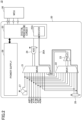
- FIG. 1 is a diagram illustrating a configuration of a diagnostic system 10 according to the one embodiment.
- a diagnostic system 10 illustrated in FIG. 1 is provided with an IC (Integrated Circuit) 20 and an MCU (Micro Controller Unit) 30.
- the IC 20 is an integrated circuit that executes predetermined processing on a sensor signal output from a sensor. For example, the IC 20 can convert the sensor signal output from the sensor from an analog signal to a digital signal.
- the IC 20 has a "diagnostic mode". In the "diagnostic mode," the IC 20 generates a test signal by a test signal generation source 26 provided inside, and, by feeding the test signal into a processing path 20A of the sensor signal, can execute a series of processing on the test signal (same processing as executed on the sensor signal).
- the MCU 30 is an example of a "determination means” that obtains from the IC 20 the test signal after the series of processing has been executed, and based on the obtained test signal, can execute determination on fault diagnosis of the IC
- the IC 20 includes a first multiplexer 21, a second multiplexer 22, a PGA (Programmable Gain Amplifier) 23, an A-D converter 24, a digital processing circuit 25, a test signal generation source 26, an internal sensor 27 (e.g., a temperature sensor), and a power supply 28.
- the IC 20 is provided with three pairs of input terminals A0P, A0M, A1P, A1M, A2P, and A2M, where each pair includes two input terminals (a +terminal and a -terminal). Accordingly, the IC 20 can be connected with three sensors, and for each pair of input terminals, two output signal lines connected to a differential sensor, or one output signal line connected to a single-ended sensor can be connected.
- the first multiplexer 21 (denoted as MUX0 in the figure) is connected to each of the multiple input terminals and the internal sensor 27.
- the first multiplexer 21 selects one of sensor signals from among multiple sensor signals input from the multiple input terminals and the internal sensor 27, to output the selected one of the sensor signals to the A-D converter 24.
- the first multiplexer 21 is an example of a "switching means" that is connected to the test signal generation source 26, and can select a test signal output from the test signal generation source 26, to output the test signal to the A-D converter 24.
- the second multiplexer 22 (denoted as MUX1 in the figure) is connected to each of the multiple input terminals and the internal sensor 27.
- the second multiplexer 22 selects one of the sensor signals from among the multiple sensor signals input from the multiple input terminals and the internal sensor 27, to output the selected one of the sensor signals to the PGA 23.
- the second multiplexer 22 is an example of a "switching means" that is connected to the test signal generation source 26, and can select the test signal output from the test signal generation source 26, to output the test signal to the PGA 23.
- the PGA 23 is connected between the output terminals of the second multiplexer 22 and the input terminals of the first multiplexer 21.
- the PGA 23 is an amplifier whose gain can be changed.
- the PGA 23 amplifies one of the sensor signals output from the second multiplexer 22, to output the amplified signal to the input terminals of the first multiplexer 21.
- the first multiplexer 21 can select the one of the sensor signals output from the PGA 23, to output the one of the sensor signals to the A-D converter 24.
- the first multiplexer 21 can output the one of the sensor signals amplified by the PGA 23 to the A-D converter 24.
- the A-D converter 24 (denoted as "ADC” in the figure) is connected to the output terminals of the first multiplexer 21.
- the A-D converter 24 converts one of the sensor signals (one sensor signal not amplified by the PGA 23 or one sensor signal amplified by the PGA 23) output from the first multiplexer 21, from an analog signal to a digital signal, to output the converted signal to the digital processing circuit 25.
- the digital processing circuit 25 is connected to the output terminal of the A-D converter 24.
- the digital processing circuit 25 includes a register 25A.
- the register 25A stores one sensor signal output from the A-D converter 24.
- the digital processing circuit 25 applies predetermined digital signal processing (e.g., digital filtering, data transmission to the MCU 30 via I2C communication, etc.) to one sensor signal (digital signal) output from the A-D converter 24 or one sensor signal (digital signal) stored in the register 25A.
- predetermined digital signal processing e.g., digital filtering, data transmission to the MCU 30 via I2C communication, etc.
- the digital processing circuit 25 outputs one sensor signal stored in the register 25A to the MCU 30 via the output terminal of the IC 20.
- the test signal generation source 26 In the "diagnostic mode", the test signal generation source 26 generates a test signal for self-diagnosis to self-diagnose the state of the processing path 20A of the sensor signal, and feeds the test signal into the processing path 20A of the sensor signal.
- the output terminals of the test signal generation source 26 are connected to both of the input terminals of the first multiplexer 21 and the input terminals of the second multiplexer 22.
- the processing path 20A of the sensor signal into which the test signal is fed includes, as processing blocks, the second multiplexer 22, the PGA 23, the first multiplexer 21, and the A-D converter 24.
- the power supply 28 generates electric power required for the respective components of the IC 20 (the PGA 23, the A-D converter 24, and the digital processing circuit 25), to supply the electric power to the respective components of the IC 20 (the PGA 23, the A-D converter 24, and the digital processing circuit 25).
- FIG. 2 is a diagram illustrating a processing path 20A in the IC 20 according to the one embodiment.
- the processing path 20A in the IC 20 is indicated by an arrow.
- a test signal generated by the test signal generation source 26 is fed into the signal processing path 20A of the sensor signal. Then, the test signal fed into the processing path 20A is input into the PGA 23 via the second multiplexer 22, and amplified by the PGA 23 with a predetermined gain.
- the test signal amplified by the PGA 23 is input into the A-D converter 24 through the first multiplexer 21, and converted from an analog signal to a digital signal by the A-D converter 24.
- the test signal converted to the digital signal by the A-D converter 24 is stored in the register 25A of the digital processing circuit 25.
- the test signal generation source 26 feeds two test signals S1 and S2 sequentially into the path illustrated in FIG. 2 .
- the PGA 23 causes the gain of the test signal S1 fed first and the gain of the test signal S2 fed second to be different from each other.
- the PGA 23 amplifies the test signal S1 with a gain of 16 times, and amplifies the test signal S2 with a gain of 32 times (i.e., twice the gain of the test signal S1). Accordingly, the test signal S1 amplified 16 times and the test signal S2 amplified 32 times are stored in the register 25A of the digital processing circuit 25.
- the two test signals S1 and S2 stored in the register 25A of the digital processing circuit 25 are read by the MCU 30, to be used for determining a diagnostic result of the IC 20.
- FIG. 3 is a flow chart illustrating the order of operations in the diagnostic mode executed by the IC 20 according to the one embodiment.
- the IC 20 is activated when the power is switched on by a user (Step S301).
- the IC 20 determines whether or not the mode has been switched to the "diagnostic mode” (Step S302). For example, the IC 20 determines that the mode has been switched to the "diagnostic mode” when the user has made settings to switch the register to the "diagnostic mode.”
- Step S302 If it is determined at Step S302 that the mode has not been switched to the "diagnostic mode" (NO at Step S302), the IC 20 executes the determination process at Step S302 again.
- Step S302 determines whether a predetermined processing execution command has been input from the user (Step S303).
- Step S303 If it is determined at Step S303 that a predetermined processing execution command has not been input (NO at Step S303), the IC 20 executes the determination process at Step S303 again.
- Step S303 if it is determined at Step S303 that a predetermined processing execution command has been input (YES at Step S303), the IC 20 switches the first multiplexer 21 and the second multiplexer 22 so as to have a test signal fed into the processing path 20A of the sensor signal (Step S304).
- the IC 20 causes the test signal generation source 26 to generate a first test signal S1, and to feed the test signal S1 into the sensor signal processing path 20A (Step S305).
- the digital processing circuit 25 stores the test signal S1 output from the A-D converter 24 (i.e., the test signal S1 after the series of processing has been executed) in the register 25A (Step S306).
- the IC 20 determines whether or not a process for the second test signal S2 has been completed (i.e., whether or not both test signals S1 and S2 were stored in the register 25A) (Step S307).
- Step S307 If it is determined at Step S307 that a process for the second test signal S2 has not been completed (NO at Step S307), the IC 20 changes the gain of the PGA 23 to twice the gain of the first time (Step S308), and then, executes steps from Steps S305 to S306 again to execute the series of processing on the second test signal S2, and stores the test signal S2 after the series of processing has been executed, in the register 25A.
- Step S307 if it is determined at Step S307 that the process for the second test signal S2 has been completed (YES at Step S307), the IC 20 ends the series of processing illustrated in FIG. 3 .
- the predetermined processing execution command described above is common to that in the "normal operation mode".
- the IC 20 feeds a sensor signal into the processing path 20A of the sensor signal, to execute a series of processing (amplification processing and A-D conversion processing) on the sensor signal.
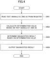
- FIG. 4 is a flow chart illustrating steps of a determination process executed by the MCU 30 according to the one embodiment.
- the MCU 30 reads the two test signals S1 and S2 from the register 25A provided in the IC 20 (Step S401).
- the MCU 30 calculates a determination value based on the two test signals S1 and S2 according to a predetermined calculation formula (Step S402). Then, the MCU 30 determines the diagnostic result of the IC 20, based on the determination value calculated at Step S402 (Step S403).
- the MCU 30 calculates the determination value according to the predetermined calculation formula ⁇ S2/S1 ⁇ . Then, the MCU 30 determines that the diagnostic result of the IC 20 is "normal” if the calculated determination value is within a predetermined numerical range centered around "2" (e.g., 1.9 to 2.1). On the other hand, the MCU 30 determines that the diagnostic result of the IC 20 is "abnormal” if the calculated determination value is outside the predetermined numerical range centered around "2". A determination result being "abnormal” indicates that there is an abnormality at some location related to the processing path 20A inside the IC 20 (the PGA 23, the A-D converter 24, the power supply 28, etc.).
- the gain used when amplifying the second test signal S2 by the PGA 23 is set to twice (i.e. 32 times) the gain (16 times) used when amplifying the first test signal S1 by the PGA 23, and hence, if there is no abnormality along the processing path 20A of the sensor signal to which the two test signals S1 and S2 are fed, the determination value calculated by the predetermined calculation formula (S2/S1) should be "2".
- the MCU 30 outputs the diagnosis result ("normal” or "abnormal") determined at Step S403 by a predetermined output method (Step S404), and ends the series of processing illustrated in FIG. 4 .
- a predetermined output method for example, a method of outputting to a higher-level application, to cause the higher-level application to notify the user by a predetermined notice method (e.g., display, audio output, etc.), may be considered.
- the predetermined output method may be a method of storing the diagnostic result in a memory, a method of transmitting the diagnostic result to the outside, or the like.
- the IC 20 is the IC 20 that executes processing on a sensor signal input from a sensor via the input terminal, and is provided with the processing path 20A that executes a series of processing on the sensor signal, and the test signal generation source 26 that generates a test signal for self-diagnosis, and feeds the test signal into the processing path 20A.
- the IC 20 according to the one embodiment can execute self-diagnosis with a stable test signal that is not affected by the connection state of the sensor to the input terminal.
- the IC 20 according to the one embodiment it is obvious that the IC 20 is abnormal if the value of the test signal output from the IC 20 is abnormal, and the IC 20 is normal if the value of the test signal output from the IC 20 is normal. Therefore, by the IC 20 according to the one embodiment, whether or not the IC 20 is functioning normally can be determined easily and securely.
- the IC 20 further includes the first multiplexer 21 and the second multiplexer 22 that switch a signal to be fed into the processing path 20A from a sensor signal to a test signal.
- feeding of a test signal from the test signal generation source 26 to the processing path 20A for a sensor signal can be implemented with a relatively simple configuration. Also, the IC 20 according to the one embodiment can easily make switching between the "normal operation mode" and the "diagnostic mode.”
- the test signal generation source 26 feeds multiple test signals sequentially into the processing path 20A, and the PGA 23 provided in the processing path 20A amplifies the multiple test signals with respective gains different from one another.
- the IC 20 can determine relatively easily and securely whether or not the multiple test signals output from the processing path 20A have been amplified normally, by comparing the values of the multiple test signals.
- the diagnostic system 10 includes the IC 20, and the MCU 30 that has a function as a determination device to determine a result of self-diagnosis of the IC 20, based on a test signal after a series of processing has been executed on the processing path 20A.
- the diagnostic system 10 can determine easily and securely by the MCU 30, whether or not the IC 20 is functioning normally.
- the function as the "determination device” is provided in the MCU 30 outside the IC 20, it is not limited as such; the function as the "determination device” may be provided inside the IC 20 (digital processing circuit 25) or on an external device other than the MCU 30.
- the present invention is applied to the IC 20 that executes amplification and A-D conversion of a sensor signal, it is not limited as such; the present invention can be applied to any integrated circuit that can execute some processing on a sensor signal.
- the IC 20 described in the above embodiment may be used, in a load detector that detects the load applied to an object, as a what-is-called AFE (Analog Front End) that connects a strain gauge to output an analog signal and a microcomputer to execute digital processing to amplify and A-D convert the analog signal.
- AFE Analog Front End
- the connection is not limited as such; the IC 20 may be connected to a sensor other than a strain gauge, and may be used in a system configuration other than the detection system 10 described in the embodiment as above.
Landscapes
- Physics & Mathematics (AREA)
- General Physics & Mathematics (AREA)
- Engineering & Computer Science (AREA)
- Environmental & Geological Engineering (AREA)
- Computer Hardware Design (AREA)
- Microelectronics & Electronic Packaging (AREA)
- General Engineering & Computer Science (AREA)
- Tests Of Electronic Circuits (AREA)
- Analogue/Digital Conversion (AREA)
- Semiconductor Integrated Circuits (AREA)
Claims (5)
- Integrierte Schaltung (20), die eine Verarbeitung an einem von einem Sensor über ein Eingabeterminal eingegebenen Sensorsignal ausführt, umfassend:einen Verarbeitungspfad (20A), durch den eine Verarbeitungsreihe an dem Sensorsignal ausgeführt wird;eine Prüfsignalerzeugungsquelle (26), die dazu konfiguriert ist, ein Prüfsignal für eine Selbstdiagnose zu erzeugen und das Prüfsignal in den Verarbeitungspfad einzuspeisen;ein Register (25A), das dazu konfiguriert ist, das Prüfsignal zu speichern; undein Bestimmungsmittel (30), das dazu konfiguriert ist, ein Ergebnis der Selbstdiagnose auf Basis des Prüfsignals zu bestimmen, nachdem die Verarbeitungsreihe durch den Verarbeitungspfad ausgeführt wurde,wobei der Verarbeitungspfad einen Verstärker (23) beinhaltet, der dazu konfiguriert ist, das Prüfsignal mit einer variablen Verstärkung zu verstärken,wobei die Prüfsignalerzeugungsquelle eine Vielzahl von Prüfsignalen nacheinander in den Verarbeitungspfad einspeist,wobei der Verstärker dazu konfiguriert ist, ein erstes Prüfsignal der Vielzahl von Prüfsignalen mit einer ersten Verstärkung zu verstärken, und ein zweites Prüfsignal der Vielzahl von Prüfsignalen mit einer zweiten Verstärkung, die sich von der ersten Verstärkung unterscheidet, zu verstärken,wobei das Register dazu konfiguriert ist, ein erstes verarbeitetes Signal zu speichern, das das mit der ersten Verstärkung verstärkte erste Prüfsignal ist, und ein zweites verarbeitetes Signal zu speichern, das das mit der zweiten Verstärkung verstärkte zweite Prüfsignal ist, undwobei das Bestimmungsmittel dazu konfiguriert ist, das Ergebnis der Selbstdiagnose auf Basis des ersten verarbeiteten Signals und des zweiten verarbeiteten Signals zu bestimmen.
- Integrierte Schaltung wie in Anspruch 1 beansprucht, ferner umfassend:
ein Umschaltmittel (21, 22), das dazu konfiguriert ist, ein in den Verarbeitungspfad (20A) eingespeistes Signal von dem Sensorsignal in das Prüfsignal umzuschalten. - Integrierte Schaltung wie in Anspruch 2 beansprucht, wobei die integrierte Schaltung einen normalen Betriebsmodus und einen Diagnosemodus aufweist, und
wobei das Umschaltmittel das Sensorsignal in dem normalen Betriebsmodus in den Verarbeitungspfad einspeist und das Prüfsignal in dem Diagnosemodus in den Verarbeitungspfad einspeist. - Integrierte Schaltung wie in einem der Ansprüche 1 bis 3 beansprucht, wobei der Verarbeitungspfad (20A) einen A-D-Wandler (24) beinhaltet, um das Prüfsignal von einem analogen Signal in ein digitales Signal umzuwandeln.
- Diagnosesystem (10), umfassend:die integrierte Schaltung wie in einem der Ansprüche 1 bis 4 beansprucht, undeine Bestimmungsvorrichtung, die dazu konfiguriert ist, ein Ergebnis der Selbstdiagnose auf Basis des Prüfsignals zu bestimmen, nachdem die Verarbeitungsreihe durch den Verarbeitungspfad ausgeführt wurde.
Applications Claiming Priority (2)
| Application Number | Priority Date | Filing Date | Title |
|---|---|---|---|
| JP2020070470A JP2021167739A (ja) | 2020-04-09 | 2020-04-09 | 集積回路 |
| PCT/JP2021/013282 WO2021205925A1 (ja) | 2020-04-09 | 2021-03-29 | 集積回路 |
Publications (3)
| Publication Number | Publication Date |
|---|---|
| EP4135017A1 EP4135017A1 (de) | 2023-02-15 |
| EP4135017A4 EP4135017A4 (de) | 2023-09-27 |
| EP4135017B1 true EP4135017B1 (de) | 2025-05-07 |
Family
ID=78023734
Family Applications (1)
| Application Number | Title | Priority Date | Filing Date |
|---|---|---|---|
| EP21784584.1A Active EP4135017B1 (de) | 2020-04-09 | 2021-03-29 | Integrierte schaltung |
Country Status (4)
| Country | Link |
|---|---|
| EP (1) | EP4135017B1 (de) |
| JP (1) | JP2021167739A (de) |
| CN (1) | CN115398252A (de) |
| WO (1) | WO2021205925A1 (de) |
Family Cites Families (14)
| Publication number | Priority date | Publication date | Assignee | Title |
|---|---|---|---|---|
| JPH04150415A (ja) * | 1990-10-11 | 1992-05-22 | Mitsubishi Electric Corp | 集積回路装置 |
| JPH0856160A (ja) * | 1994-08-10 | 1996-02-27 | Nissin Electric Co Ltd | Adコンバータの異常検出装置 |
| US6408412B1 (en) * | 1999-09-03 | 2002-06-18 | Advantest Corp. | Method and structure for testing embedded analog/mixed-signal cores in system-on-a-chip |
| US7135881B2 (en) * | 2004-12-21 | 2006-11-14 | Teradyne, Inc. | Method and system for producing signals to test semiconductor devices |
| JP4379445B2 (ja) * | 2006-07-27 | 2009-12-09 | 株式会社デンソー | Ad変換器の故障検出装置 |
| JP4801180B2 (ja) * | 2009-03-06 | 2011-10-26 | 株式会社日立製作所 | 多チャンネルアナログ入出力回路の故障診断装置及び故障診断方法 |
| US20110273197A1 (en) * | 2010-05-07 | 2011-11-10 | Qualcomm Incorporated | Signal generator for a built-in self test |
| JP2012151666A (ja) * | 2011-01-19 | 2012-08-09 | Renesas Electronics Corp | 半導体集積回路およびその検査方法 |
| JP2013257178A (ja) * | 2012-06-11 | 2013-12-26 | Asahi Kasei Electronics Co Ltd | 半導体装置、自己診断システム、それらを用いた車載装置および医療装置 |
| CN103308850B (zh) * | 2013-07-03 | 2016-02-24 | 苏州磐启微电子有限公司 | 触控ic模拟前端自测的内建架构及测试方法 |
| JP6500522B2 (ja) * | 2015-03-16 | 2019-04-17 | セイコーエプソン株式会社 | 回路装置、物理量検出装置、電子機器及び移動体 |
| JP5980377B2 (ja) | 2015-06-11 | 2016-08-31 | キヤノン株式会社 | アナログデジタル変換回路、アナログデジタル変換回路の検査方法、撮像装置、撮像装置を有する撮像システム、撮像装置の検査方法 |
| EP3330858B1 (de) * | 2015-07-29 | 2022-05-25 | Hitachi Astemo, Ltd. | Bordeigene steuerungsvorrichtung, bordeigene integrierte schaltung |
| JP2020070470A (ja) | 2018-10-31 | 2020-05-07 | 旭化成株式会社 | 学習処理装置、学習処理方法、化合物半導体の製造方法およびプログラム |
-
2020
- 2020-04-09 JP JP2020070470A patent/JP2021167739A/ja active Pending
-
2021
- 2021-03-29 WO PCT/JP2021/013282 patent/WO2021205925A1/ja not_active Ceased
- 2021-03-29 CN CN202180024450.2A patent/CN115398252A/zh active Pending
- 2021-03-29 EP EP21784584.1A patent/EP4135017B1/de active Active
Also Published As
| Publication number | Publication date |
|---|---|
| WO2021205925A1 (ja) | 2021-10-14 |
| EP4135017A4 (de) | 2023-09-27 |
| JP2021167739A (ja) | 2021-10-21 |
| EP4135017A1 (de) | 2023-02-15 |
| CN115398252A (zh) | 2022-11-25 |
Similar Documents
| Publication | Publication Date | Title |
|---|---|---|
| US8131507B2 (en) | Sensor apparatus | |
| US20150204745A1 (en) | Strain gauge pressure sensor circuit with sensor disconnect detection | |
| US8103400B2 (en) | Sensor apparatus | |
| US8717037B2 (en) | Electronic control device | |
| EP3222976B1 (de) | Feldvorrichtung und -detektor | |
| EP4135017B1 (de) | Integrierte schaltung | |
| JP6443356B2 (ja) | ロードセル入力ユニット | |
| US20190212715A1 (en) | Signal processing device and control method of signal processing device | |
| US8131508B2 (en) | Sensor apparatus | |
| US9574925B2 (en) | Fluid measurement device having a circuit for precise flow measurement | |
| KR102280208B1 (ko) | 로드셀의 이상 상태를 감지하는 서밍카드 및 그 동작 방법 | |
| JPH08247881A (ja) | センサ診断機能付差圧・圧力伝送器 | |
| KR101067461B1 (ko) | 필드 기기 | |
| US20230353162A1 (en) | Semiconductor device and failure detection method | |
| JP2001035335A (ja) | リレー故障検出装置 | |
| JP2010009344A (ja) | フィールド機器 | |
| EP4135033A1 (de) | Integrierte schaltung | |
| JP5088207B2 (ja) | アナログ出力装置 | |
| US7576643B2 (en) | Sensor for measuring physical variables and for passing on the measured variable, circuit having such a sensor and method for operating the sensor and the circuit | |
| US11676477B2 (en) | Fire alarm system | |
| JPH07245865A (ja) | 配電盤とデジタル継電装置 | |
| JP2026018111A (ja) | アナログ入力モジュール、及び、制御システム | |
| JPH07248882A (ja) | アナログ入力処理装置 | |
| CN118264250A (zh) | 多通道模拟信号采样装置、方法、控制器和车辆 | |
| CN112462123A (zh) | 一种宽输入交直流电压隔离采集电路 |
Legal Events
| Date | Code | Title | Description |
|---|---|---|---|
| STAA | Information on the status of an ep patent application or granted ep patent |
Free format text: STATUS: THE INTERNATIONAL PUBLICATION HAS BEEN MADE |
|
| PUAI | Public reference made under article 153(3) epc to a published international application that has entered the european phase |
Free format text: ORIGINAL CODE: 0009012 |
|
| STAA | Information on the status of an ep patent application or granted ep patent |
Free format text: STATUS: REQUEST FOR EXAMINATION WAS MADE |
|
| 17P | Request for examination filed |
Effective date: 20221005 |
|
| AK | Designated contracting states |
Kind code of ref document: A1 Designated state(s): AL AT BE BG CH CY CZ DE DK EE ES FI FR GB GR HR HU IE IS IT LI LT LU LV MC MK MT NL NO PL PT RO RS SE SI SK SM TR |
|
| DAV | Request for validation of the european patent (deleted) | ||
| DAX | Request for extension of the european patent (deleted) | ||
| REG | Reference to a national code |
Ref country code: DE Ref legal event code: R079 Free format text: PREVIOUS MAIN CLASS: H01L0021822000 Ipc: G01R0031280000 Ref country code: DE Ref legal event code: R079 Ref document number: 602021030521 Country of ref document: DE Free format text: PREVIOUS MAIN CLASS: H01L0021822000 Ipc: G01R0031280000 |
|
| A4 | Supplementary search report drawn up and despatched |
Effective date: 20230830 |
|
| RIC1 | Information provided on ipc code assigned before grant |
Ipc: G01D 3/08 20060101ALI20230824BHEP Ipc: G01D 21/00 20060101ALI20230824BHEP Ipc: G01R 31/28 20060101AFI20230824BHEP |
|
| GRAP | Despatch of communication of intention to grant a patent |
Free format text: ORIGINAL CODE: EPIDOSNIGR1 |
|
| STAA | Information on the status of an ep patent application or granted ep patent |
Free format text: STATUS: GRANT OF PATENT IS INTENDED |
|
| INTG | Intention to grant announced |
Effective date: 20250115 |
|
| RIN1 | Information on inventor provided before grant (corrected) |
Inventor name: TAKEHANA, HIROAKI Inventor name: OTSUKA, SHINYA |
|
| GRAS | Grant fee paid |
Free format text: ORIGINAL CODE: EPIDOSNIGR3 |
|
| GRAA | (expected) grant |
Free format text: ORIGINAL CODE: 0009210 |
|
| STAA | Information on the status of an ep patent application or granted ep patent |
Free format text: STATUS: THE PATENT HAS BEEN GRANTED |
|
| AK | Designated contracting states |
Kind code of ref document: B1 Designated state(s): AL AT BE BG CH CY CZ DE DK EE ES FI FR GB GR HR HU IE IS IT LI LT LU LV MC MK MT NL NO PL PT RO RS SE SI SK SM TR |
|
| REG | Reference to a national code |
Ref country code: GB Ref legal event code: FG4D |
|
| REG | Reference to a national code |
Ref country code: CH Ref legal event code: EP |
|
| REG | Reference to a national code |
Ref country code: DE Ref legal event code: R096 Ref document number: 602021030521 Country of ref document: DE |
|
| REG | Reference to a national code |
Ref country code: IE Ref legal event code: FG4D |
|
| P01 | Opt-out of the competence of the unified patent court (upc) registered |
Free format text: CASE NUMBER: APP_23996/2025 Effective date: 20250520 |
|
| REG | Reference to a national code |
Ref country code: NL Ref legal event code: MP Effective date: 20250507 |
|
| PG25 | Lapsed in a contracting state [announced via postgrant information from national office to epo] |
Ref country code: PT Free format text: LAPSE BECAUSE OF FAILURE TO SUBMIT A TRANSLATION OF THE DESCRIPTION OR TO PAY THE FEE WITHIN THE PRESCRIBED TIME-LIMIT Effective date: 20250908 Ref country code: FI Free format text: LAPSE BECAUSE OF FAILURE TO SUBMIT A TRANSLATION OF THE DESCRIPTION OR TO PAY THE FEE WITHIN THE PRESCRIBED TIME-LIMIT Effective date: 20250507 Ref country code: ES Free format text: LAPSE BECAUSE OF FAILURE TO SUBMIT A TRANSLATION OF THE DESCRIPTION OR TO PAY THE FEE WITHIN THE PRESCRIBED TIME-LIMIT Effective date: 20250507 |
|
| REG | Reference to a national code |
Ref country code: LT Ref legal event code: MG9D |
|
| PG25 | Lapsed in a contracting state [announced via postgrant information from national office to epo] |
Ref country code: GR Free format text: LAPSE BECAUSE OF FAILURE TO SUBMIT A TRANSLATION OF THE DESCRIPTION OR TO PAY THE FEE WITHIN THE PRESCRIBED TIME-LIMIT Effective date: 20250808 Ref country code: NO Free format text: LAPSE BECAUSE OF FAILURE TO SUBMIT A TRANSLATION OF THE DESCRIPTION OR TO PAY THE FEE WITHIN THE PRESCRIBED TIME-LIMIT Effective date: 20250807 |
|
| PG25 | Lapsed in a contracting state [announced via postgrant information from national office to epo] |
Ref country code: NL Free format text: LAPSE BECAUSE OF FAILURE TO SUBMIT A TRANSLATION OF THE DESCRIPTION OR TO PAY THE FEE WITHIN THE PRESCRIBED TIME-LIMIT Effective date: 20250507 Ref country code: PL Free format text: LAPSE BECAUSE OF FAILURE TO SUBMIT A TRANSLATION OF THE DESCRIPTION OR TO PAY THE FEE WITHIN THE PRESCRIBED TIME-LIMIT Effective date: 20250507 |
|
| REG | Reference to a national code |
Ref country code: AT Ref legal event code: MK05 Ref document number: 1793013 Country of ref document: AT Kind code of ref document: T Effective date: 20250507 |
|
| PG25 | Lapsed in a contracting state [announced via postgrant information from national office to epo] |
Ref country code: BG Free format text: LAPSE BECAUSE OF FAILURE TO SUBMIT A TRANSLATION OF THE DESCRIPTION OR TO PAY THE FEE WITHIN THE PRESCRIBED TIME-LIMIT Effective date: 20250507 |
|
| PG25 | Lapsed in a contracting state [announced via postgrant information from national office to epo] |
Ref country code: HR Free format text: LAPSE BECAUSE OF FAILURE TO SUBMIT A TRANSLATION OF THE DESCRIPTION OR TO PAY THE FEE WITHIN THE PRESCRIBED TIME-LIMIT Effective date: 20250507 |
|
| PG25 | Lapsed in a contracting state [announced via postgrant information from national office to epo] |
Ref country code: AT Free format text: LAPSE BECAUSE OF FAILURE TO SUBMIT A TRANSLATION OF THE DESCRIPTION OR TO PAY THE FEE WITHIN THE PRESCRIBED TIME-LIMIT Effective date: 20250507 |
|
| PG25 | Lapsed in a contracting state [announced via postgrant information from national office to epo] |
Ref country code: RS Free format text: LAPSE BECAUSE OF FAILURE TO SUBMIT A TRANSLATION OF THE DESCRIPTION OR TO PAY THE FEE WITHIN THE PRESCRIBED TIME-LIMIT Effective date: 20250807 |
|
| PG25 | Lapsed in a contracting state [announced via postgrant information from national office to epo] |
Ref country code: IS Free format text: LAPSE BECAUSE OF FAILURE TO SUBMIT A TRANSLATION OF THE DESCRIPTION OR TO PAY THE FEE WITHIN THE PRESCRIBED TIME-LIMIT Effective date: 20250907 |
|
| PG25 | Lapsed in a contracting state [announced via postgrant information from national office to epo] |
Ref country code: LV Free format text: LAPSE BECAUSE OF FAILURE TO SUBMIT A TRANSLATION OF THE DESCRIPTION OR TO PAY THE FEE WITHIN THE PRESCRIBED TIME-LIMIT Effective date: 20250507 |
|
| PG25 | Lapsed in a contracting state [announced via postgrant information from national office to epo] |
Ref country code: DK Free format text: LAPSE BECAUSE OF FAILURE TO SUBMIT A TRANSLATION OF THE DESCRIPTION OR TO PAY THE FEE WITHIN THE PRESCRIBED TIME-LIMIT Effective date: 20250507 Ref country code: SM Free format text: LAPSE BECAUSE OF FAILURE TO SUBMIT A TRANSLATION OF THE DESCRIPTION OR TO PAY THE FEE WITHIN THE PRESCRIBED TIME-LIMIT Effective date: 20250507 |
|
| PG25 | Lapsed in a contracting state [announced via postgrant information from national office to epo] |
Ref country code: CZ Free format text: LAPSE BECAUSE OF FAILURE TO SUBMIT A TRANSLATION OF THE DESCRIPTION OR TO PAY THE FEE WITHIN THE PRESCRIBED TIME-LIMIT Effective date: 20250507 |
|
| PG25 | Lapsed in a contracting state [announced via postgrant information from national office to epo] |
Ref country code: EE Free format text: LAPSE BECAUSE OF FAILURE TO SUBMIT A TRANSLATION OF THE DESCRIPTION OR TO PAY THE FEE WITHIN THE PRESCRIBED TIME-LIMIT Effective date: 20250507 |
|
| PG25 | Lapsed in a contracting state [announced via postgrant information from national office to epo] |
Ref country code: SK Free format text: LAPSE BECAUSE OF FAILURE TO SUBMIT A TRANSLATION OF THE DESCRIPTION OR TO PAY THE FEE WITHIN THE PRESCRIBED TIME-LIMIT Effective date: 20250507 |
|
| PG25 | Lapsed in a contracting state [announced via postgrant information from national office to epo] |
Ref country code: IT Free format text: LAPSE BECAUSE OF FAILURE TO SUBMIT A TRANSLATION OF THE DESCRIPTION OR TO PAY THE FEE WITHIN THE PRESCRIBED TIME-LIMIT Effective date: 20250507 |
|
| REG | Reference to a national code |
Ref country code: DE Ref legal event code: R097 Ref document number: 602021030521 Country of ref document: DE |
|
| PLBE | No opposition filed within time limit |
Free format text: ORIGINAL CODE: 0009261 |
|
| STAA | Information on the status of an ep patent application or granted ep patent |
Free format text: STATUS: NO OPPOSITION FILED WITHIN TIME LIMIT |
|
| REG | Reference to a national code |
Ref country code: CH Ref legal event code: L10 Free format text: ST27 STATUS EVENT CODE: U-0-0-L10-L00 (AS PROVIDED BY THE NATIONAL OFFICE) Effective date: 20260318 |
|
| PGFP | Annual fee paid to national office [announced via postgrant information from national office to epo] |
Ref country code: DE Payment date: 20260319 Year of fee payment: 6 |
|
| 26N | No opposition filed |
Effective date: 20260210 |