EP4131289A1 - Verbindungsstruktur für kohlenstoffnanoröhrchendraht - Google Patents
Verbindungsstruktur für kohlenstoffnanoröhrchendraht Download PDFInfo
- Publication number
- EP4131289A1 EP4131289A1 EP21780030.9A EP21780030A EP4131289A1 EP 4131289 A1 EP4131289 A1 EP 4131289A1 EP 21780030 A EP21780030 A EP 21780030A EP 4131289 A1 EP4131289 A1 EP 4131289A1
- Authority
- EP
- European Patent Office
- Prior art keywords
- wire
- carbon nanotube
- cnt
- connection structure
- nanotube wire
- Prior art date
- Legal status (The legal status is an assumption and is not a legal conclusion. Google has not performed a legal analysis and makes no representation as to the accuracy of the status listed.)
- Withdrawn
Links
Images


Classifications
-
- H—ELECTRICITY
- H01—ELECTRIC ELEMENTS
- H01B—CABLES; CONDUCTORS; INSULATORS; SELECTION OF MATERIALS FOR THEIR CONDUCTIVE, INSULATING OR DIELECTRIC PROPERTIES
- H01B1/00—Conductors or conductive bodies characterised by the conductive materials; Selection of materials as conductors
- H01B1/04—Conductors or conductive bodies characterised by the conductive materials; Selection of materials as conductors mainly consisting of carbon-silicon compounds, carbon or silicon
-
- H—ELECTRICITY
- H01—ELECTRIC ELEMENTS
- H01R—ELECTRICALLY-CONDUCTIVE CONNECTIONS; STRUCTURAL ASSOCIATIONS OF A PLURALITY OF MUTUALLY-INSULATED ELECTRICAL CONNECTING ELEMENTS; COUPLING DEVICES; CURRENT COLLECTORS
- H01R4/00—Electrically-conductive connections between two or more conductive members in direct contact, i.e. touching one another; Means for effecting or maintaining such contact; Electrically-conductive connections having two or more spaced connecting locations for conductors and using contact members penetrating insulation
- H01R4/02—Soldered or welded connections
- H01R4/028—Soldered or welded connections comprising means for preventing flowing or wicking of solder or flux in parts not desired
-
- C—CHEMISTRY; METALLURGY
- C01—INORGANIC CHEMISTRY
- C01B—NON-METALLIC ELEMENTS; COMPOUNDS THEREOF; METALLOIDS OR COMPOUNDS THEREOF NOT COVERED BY SUBCLASS C01C
- C01B32/00—Carbon; Compounds thereof
- C01B32/15—Nano-sized carbon materials
- C01B32/158—Carbon nanotubes
- C01B32/168—After-treatment
-
- D—TEXTILES; PAPER
- D01—NATURAL OR MAN-MADE THREADS OR FIBRES; SPINNING
- D01F—CHEMICAL FEATURES IN THE MANUFACTURE OF ARTIFICIAL FILAMENTS, THREADS, FIBRES, BRISTLES OR RIBBONS; APPARATUS SPECIALLY ADAPTED FOR THE MANUFACTURE OF CARBON FILAMENTS
- D01F9/00—Artificial filaments or the like of other substances; Manufacture thereof; Apparatus specially adapted for the manufacture of carbon filaments
- D01F9/08—Artificial filaments or the like of other substances; Manufacture thereof; Apparatus specially adapted for the manufacture of carbon filaments of inorganic material
- D01F9/12—Carbon filaments; Apparatus specially adapted for the manufacture thereof
-
- H—ELECTRICITY
- H01—ELECTRIC ELEMENTS
- H01R—ELECTRICALLY-CONDUCTIVE CONNECTIONS; STRUCTURAL ASSOCIATIONS OF A PLURALITY OF MUTUALLY-INSULATED ELECTRICAL CONNECTING ELEMENTS; COUPLING DEVICES; CURRENT COLLECTORS
- H01R12/00—Structural associations of a plurality of mutually-insulated electrical connecting elements, specially adapted for printed circuits, e.g. printed circuit boards [PCB], flat or ribbon cables, or like generally planar structures, e.g. terminal strips, terminal blocks; Coupling devices specially adapted for printed circuits, flat or ribbon cables, or like generally planar structures; Terminals specially adapted for contact with, or insertion into, printed circuits, flat or ribbon cables, or like generally planar structures
- H01R12/50—Fixed connections
- H01R12/51—Fixed connections for rigid printed circuits or like structures
- H01R12/53—Fixed connections for rigid printed circuits or like structures connecting to cables except for flat or ribbon cables
-
- C—CHEMISTRY; METALLURGY
- C01—INORGANIC CHEMISTRY
- C01B—NON-METALLIC ELEMENTS; COMPOUNDS THEREOF; METALLOIDS OR COMPOUNDS THEREOF NOT COVERED BY SUBCLASS C01C
- C01B2202/00—Structure or properties of carbon nanotubes
- C01B2202/08—Aligned nanotubes
-
- C—CHEMISTRY; METALLURGY
- C01—INORGANIC CHEMISTRY
- C01B—NON-METALLIC ELEMENTS; COMPOUNDS THEREOF; METALLOIDS OR COMPOUNDS THEREOF NOT COVERED BY SUBCLASS C01C
- C01B2202/00—Structure or properties of carbon nanotubes
- C01B2202/20—Nanotubes characterized by their properties
- C01B2202/26—Mechanical properties
-
- H—ELECTRICITY
- H01—ELECTRIC ELEMENTS
- H01R—ELECTRICALLY-CONDUCTIVE CONNECTIONS; STRUCTURAL ASSOCIATIONS OF A PLURALITY OF MUTUALLY-INSULATED ELECTRICAL CONNECTING ELEMENTS; COUPLING DEVICES; CURRENT COLLECTORS
- H01R13/00—Details of coupling devices of the kinds covered by groups H01R12/70 or H01R24/00 - H01R33/00
- H01R13/02—Contact members
- H01R13/025—Contact members formed by the conductors of a cable end
Definitions
- the present invention relates to a carbon nanotube wire and a connection structure for connecting the carbon nanotube wire to a connection target.
- Carbon nanotubes are materials having various characteristics and are expected to be applied in many fields. Since CNTs are lightweight and excellent in various characteristics such as electrical conductivity, thermal conductivity and mechanical strength, CNTs are expected to be applied, for example, to wires as an alternative to metal wires in applications such as electric wires.
- CNT wires When used as wires, carbon nanotube wires (hereinafter may also be referred to as "CNT wires”) need to be made longer.
- lengthening of the CNT wires requires a high-level technique.
- As a technique of lengthening conventional CNT wires it is proposed to make carbon nanotubes grown from each carbon nanotube yarn entangled with the carbon nanotube yarn on another side of connection and/or the grown carbon nanotubes, and cause the carbon nanotube yarns to be mutually connected, thus making it possible to lengthen the carbon nanotube wires (Patent Literature 1).
- Patent Literature 1 in order to make the carbon nanotubes grow from the carbon nanotube yarn, it is necessary to apply a catalyst solution to a region where the carbon nanotube yarns are mutually connected, thereby cause the carbon nanotubes to grow and make them entangled with the carbon nanotube yarns on the other side of connection, but the problem is that such connection work is complicated and the use of the catalyst solution makes it difficult to perform positional control over the region where the carbon nanotube yarns are mutually connected.
- Patent Literature 1 describing that carbon nanotubes are made to grow and entangled with the carbon nanotube yarn on the other side of connection involves a problem that when the connection destination is other than the CNT wire, it is not possible to form any connection body.
- connection work is simple and connection strength can be acquired as well.
- the CNT wire is inferior in solder wettability compared to the metal wire, and particularly when the CNT wire is a stranded wire in which the elemental wire made up of a carbon nanotube aggregate is stranded together, it is difficult for solder to penetrate into the CNT wire, showing a problem with conductivity and strength of the joint.
- the CNT wire when the CNT wire is connected to the connection target by soldering, the CNT wire needs to be subjected to hydrophilic processing or roughening treatment in advance. Therefore, when the CNT wire is soldered, there is a problem that the connection work is still complicated.
- Patent Literature 1 Japanese Patent Application Publication No. 2013-47402
- the present invention has been made in view of the above-described circumstances, and it is an object of the present invention to provide a connection structure of a carbon nanotube wire that allows the carbon nanotube wire to be connected to a connection target at a desired region with simple operation, with a joint between the carbon nanotube wire and the connection target having excellent electrical connectivity and mechanical connectivity.
- the gist of a configuration of the present invention is as follows.
- the penetrating part of the conducting wire with high solder wettability formed along a cross section having a component orthogonal to the longitudinal direction of the carbon nanotube wire, which is a stranded wire is provided, and solder penetrates the penetrating part along the conducting wire, and so it is possible to easily create a region with high solder wettability (that is, the penetrating part of the conducting wire) inside the region surrounded by a surface of the carbon nanotube aggregate at the penetrating part of the carbon nanotube wire, which is the stranded wire and the surface of the conducting wire.
- the solder flows into the carbon nanotube wire along the penetrating part of the conducting wire, the solder, the conducting wire and the connection target are connected firmly together, and as a result, the carbon nanotube wire and the connection target are connected firmly together.
- part of the conducting wire protrudes from a part of the carbon nanotube wire not facing the connection target, and so the protruding part of the conducting wire allows solder to smoothly flow into the carbon nanotube wire.
- connection structure of a carbon nanotube wire of the present invention the winding part where at least part of the conducting wire other than the region located at the penetrating part is wound around the perimeter of the carbon nanotube wire is included, and so the solder accumulates in the winding part. Therefore, solder is surely applied to the desired joint and in the vicinity, allowing the solder to flow into the carbon nanotube wire more smoothly. Moreover, since the solder is more likely to accumulate at the winding part, it is possible to prevent the solder from spreading wetly in regions other than the desired joint and in the vicinity.
- the ratio of the cross-sectional area of the penetrating part to the cross-sectional area of the carbon nanotube wire is 5% or more and 99% or less, and the solder can more reliably flow into the carbon nanotube wire, which more reliably improves connection reliability between the carbon nanotube wire and the connection target.
- FIG. 1 is an explanatory view of a connection structure in which a carbon nanotube wire, a connection structure according to the first embodiment of the present invention, is connected to a substrate.
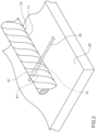
- FIG. 2 is an explanatory view illustrating that a penetrating part of a conducting wire is formed in the carbon nanotube wire to be used for the connection structure according to the first embodiment of the present invention.
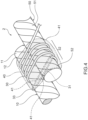
- FIG. 3 is an explanatory view illustrating an aspect that a conducting wire is wound around a perimeter of the carbon nanotube wire in which a penetrating part of the conducting wire is formed, to be used for the connection structure according to the first embodiment of the present invention.
- the connection structure 1 of a carbon nanotube wire is provided with a carbon nanotube wire (CNT wire) 10 formed by twisting and bundling carbon nanotube aggregates (hereinafter may also be referred to as "CNT aggregates") and a connection target to which the CNT wire 10 is connected.
- the connection target of the CNT wire 10 is a conductive member.
- the connection target is a substrate 20 and examples of the substrate 20 include a substrate provided with a metal member such as a substrate made of metal and a circuit substrate.
- connection structure 1 of a carbon nanotube wire the vicinity of the end of the CNT wire 10 is connected to the substrate 20 and a joint 40 between the CNT wire 10 and the substrate 20 is formed.
- Solder 41 is used for connection between the CNT wire 10 and the substrate 20. Therefore, the solder 41 connects the CNT wire 10 and the substrate 20, which is a connection target, and the CNT wire 10 is soldered to the substrate 20.
- the CNT wire 10 is formed by twisting a plurality of elemental wires composed of a carbon nanotube aggregate (CNT aggregate) formed of a plurality of carbon nanotubes (CNTs) having a layered structure with one or more layers. Therefore, the CNT wire 10 is a stranded wire formed by twisting and bundling elemental wires composed of CNT aggregates.
- the CNT wire 10 means a CNT wire 10 with a CNT ratio of 90 mass% or more. Note that when calculating the CNT ratio in the CNT wire 10, plating and dopants are excluded.
- the longitudinal direction of the CNT aggregate forms a longitudinal direction of the CNT wire 10. Therefore, the CNT aggregate is linear.
- the plurality of CNT aggregates in the CNT wire 10 are arranged with their longitudinal axes nearly aligned. Therefore, the plurality of CNT aggregates in the CNT wire 10 are oriented.
- connection structure 1 of a carbon nanotube wire is provided with a conducting wire 30 with higher solder wettability than the CNT wire 10 and a penetrating part 31 of the conducting wire 30 formed along a cross section orthogonal to a longitudinal direction of the CNT wire 10.
- the penetrating part 31 of the conducting wire 30 is formed along the cross section orthogonal to the longitudinal direction of the CNT wire 10 by causing the conducting wire 30 to penetrate the CNT wire 10 along a radial direction of the CNT wire 10.
- the conducting wire 30 penetrates along a center line of the cross section orthogonal to the longitudinal direction of the CNT wire 10.
- connection structure of a carbon nanotube wire according to the embodiment of the present invention, although the penetrating part 31 of the conducting wire 30 is formed on the cross section orthogonal to the longitudinal direction of the CNT wire 10 for convenience of explanation, the cross section is not limited to the cross section orthogonal to the longitudinal direction as long as the cross section has a component orthogonal to the longitudinal direction of the CNT wire 10.
- an extending direction of the penetrating part 31 of the conducting wire 30 is a direction substantially orthogonal to the longitudinal direction of the CNT wire 10. Since the CNT wire 10 is a stranded wire formed by twisting elemental wires composed of CNT aggregates, the conducting wire 30 can penetrate the CNT wire 10 by piercing the conducting wire 30 into the CNT wire 10 without the need to separately form a through hole or the like in the CNT wire 10. By piercing the conducting wire 30 into the CNT wire 10, a gap is formed between the CNT wire 10 and the conducting wire 30. In the connection structure 1 of a carbon nanotube wire, by piercing one conducting wire 30 into the CNT wire 10, one penetrating part 31 is formed.
- the penetrating part need not be a direction substantially orthogonal to the longitudinal direction of the CNT wire, and, for example, the conducting wire may be folded back in the CNT wire 10 and both ends of the conducting wire may protrude from any position of an outer circumference of the CNT wire 10. Therefore, the penetrating part 31 may be formed bent in the CNT wire 10.
- a structure in which solder flows into the CNT wire 10 that is, a gap formed between an outer circumference of the conducting wire 30 and the CNT aggregate
- solder flows into the CNT wire 10 that is, a gap formed between an outer circumference of the conducting wire 30 and the CNT aggregate
- a gap is also formed between the CNT wire 10 and the conducting wire 30, and so when the CNT wire 10 is soldered to the substrate 20, the solder 41 penetrates the penetrating part 31 along the conducting wire 30. That is, when the CNT wire 10 is soldered to the substrate 20, the solder flows into the gap formed between the outer circumference of the conducting wire 30 and the CNT wire 10, that is, along the inside of the CNT wire 10, and the solder 41 thereby penetrates the penetrating part 31. From above, a direction in which the solder 41 is formed is a direction substantially orthogonal to the longitudinal direction of the CNT wire 10. Note that FIG. 2 also illustrates the solder 41 applied to the penetrating part 31 when the CNT wire 10 is soldered to the substrate 20 for convenience of explanation of the connection structure 1 of a carbon nanotube wire.
- At least part of the conducting wire 30 other than the region located at the penetrating part 31 in the joint 40 is wound around the outer circumferential surface 11 of the CNT wire 10 along the circumferential direction and a winding part 32 is formed.
- the penetrating part 31 of the conducting wire 30 and the winding part 32 are mutually continuous.
- the winding part 32 is provided in the vicinity of the penetrating part 31. Note that the winding part 32 of the conducting wire 30 is provided so as to contact the outer circumferential surface 11 of the CNT wire 10.
- the solder 41 is more likely to flow into the CNT wire 10, and the connection strength between the CNT wire 10 and the substrate 20 improves.
- the winding part 32 of the conducting wire 30 Since the winding part 32 of the conducting wire 30 is formed, there is an aspect that part of the conducting wire 30 protrudes from a portion of the CNT wire 10 not facing the substrate 20. That is, the conducting wire 30 protrudes from the outer circumferential surface 11 of the CNT wire 10 at the winding part 32 of the conducting wire 30.
- a tip portion 33 of the conducting wire 30 located at the penetrating part 31 extends outward from the outer circumferential surface 11 of the CNT wire 10 so that part of the conducting wire 30 protrudes from the portion of the CNT wire 10 not facing the substrate 20.
- an end portion of the conducting wire 30 (tip portion 33) in which no penetrating part 31 is formed may be connected to the substrate 20 in advance by soldering or the like.
- the number of turns of the conducting wire 30 of the winding part 32 is not particularly limited, and may be once or a plurality of times. Note that in FIG. 3 , the number of turns of the conducting wire 30 is assumed to be 4 for convenience of explanation.
- the conducting wire 30 is wound along a circumferential direction of the CNT wire 10 at predetermined intervals in the longitudinal direction of the CNT wire 10.
- the winding part 32 has a function to store the solder 41.
- FIG. 3 also illustrates the solder 41 which is applied when the CNT wire 10 is soldered to the substrate 20 in the connection structure of a carbon nanotube wire.
- Examples of the conducting wire 30 with higher solder wettability than the CNT wire 10 include metal wires such as copper, silver, platinum and tungsten.
- the type of solder is not particularly limited if the solder can be used for connection of metal members and examples of such solder include Sn-Pbbased lead containing solder, lead-free solder such as Sn-Ag-Cu-based, Sn-Cu-based, Sn-Zn-based solder.
- the amount of the solder 41 to be applied to one penetrating part 31 is not particularly limited, but a lower limit value of the solder 41 is preferably 3.0 mg from a standpoint of improving tensile strength and electrical connectivity of the joint 40.
- an upper limit value of the solder 41 to be applied to one penetrating part 31 is preferably 20 mg from a standpoint of weight reduction, and particularly preferably 6.0 mg.
- the diameter of the CNT wire 10 is not particularly limited, but it can be, for example, 20 ⁇ m to 1 mm.
- the number of twists of elemental wires of CNT that form the CNT wire 10 is not particularly limited, but it can be, for example, 2 to 2000.
- the diameter of the conducting wire 30 is not particularly limited, but it can be, for example, 10 ⁇ m or more and 1 mm or less.
- connection structure 1 of a carbon nanotube wire the penetrating part 31 of the conducting wire 30 with high solder wettability formed along the cross section orthogonal to the longitudinal direction of the CNT wire 10, which is a stranded wire, is provided, the solder 41 penetrates the penetrating part 31 along the conducting wire 30, and it is thereby possible to easily create an inside with high solder wettability (that is, the gap formed between the outer circumference of the conducting wire 30 and the CNT wire 10) in the CNT wire 10.
- connection structure 1 of a carbon nanotube wire by selecting the position of the penetrating part 31 of the conducting wire 30 in the CNT wire 10 as appropriate, it is possible to firmly connect the CNT wire 10 and the substrate 20 at a desired region with simple operation.
- the connection structure 1 of a carbon nanotube wire can obtain a connection structure of a carbon nanotube wire in which the joint 40 between the CNT wire 10 and the substrate 20 has excellent electrical connectivity and mechanical connectivity.
- connection structure 1 of a carbon nanotube wire since part of the conducting wire 30 protrudes from a portion of the CNT wire 10 not facing the substrate 20, the protruding part of the conducting wire 30 allows the solder 41 to smoothly flow into the CNT wire 10 along the extending direction of the conducting wire 30.
- connection structure 1 of a carbon nanotube wire at least part of the conducting wire 30 other than the region located at the penetrating part 31 includes the winding part 32 wound around the outer circumferential surface 11 of the CNT wire 10, and so when the CNT wire 10 is soldered to the substrate 20, the solder 41 accumulates at the winding part 32. Therefore, the solder 41 is surely applied to the desired joint 40 and the vicinity of the joint 40, and the solder 41 can more smoothly flow into the CNT wire 10 along the extending direction of the conducting wire 30. Since the solder 41 is more likely to accumulate at the winding part 32, it is possible to prevent the solder 41 from getting wet and spreading over regions other than the desired joint 40 and in the vicinity of the joint 40.
- the ratio of the cross-sectional area of the conducting wire 30 in the penetrating part 31 to the cross-sectional area of the CNT wire 10 on a cross section orthogonal to the longitudinal direction of the CNT wire 10 is not particularly limited, the ratio is preferably 5% or more and 99% or less, more preferably 10% or more and 99% or less, and particularly preferably 30% or more and 50% or less. Especially when the cross-sectional area of the conducting wire 30 is 30% or more and 50% or less, the performance of electrical connectivity and mechanical connectivity reaches a peak, which is also preferable from a standpoint of lightweight and costs, too.
- the lower limit value of the cross-sectional area is preferably 10%, and particularly preferably 30% from a standpoint of electrical connectivity.
- the upper limit value of the ratio of the cross-sectional area is preferably 99% from a standpoint of handling performance when forming the penetrating part 31 and the winding part 32, and particularly preferably 50% from a standpoint of achieving balance between lightweight and electrical connectivity.
- the above-described ratio of the cross-sectional area is calculated by (cross-sectional area in radial direction of conducting wire 30 in penetrating part 31/cross-sectional area in radial direction of CNT wire 10) times 100.
- connection structure of a carbon nanotube wire according to a second embodiment of the present invention will be described hereinafter using the accompanying drawings. Note that since the connection structure of a carbon nanotube wire according to the second embodiment and the connection structure of a carbon nanotube wire according to the first embodiment share main components, components identical to the components of the connection structure of a carbon nanotube wire according to the first embodiment will be described using identical reference numerals.
- FIG. 4 is an explanatory view of a connection structure in which the carbon nanotube wire, the connection structure according to the second embodiment of the present invention, is connected to another carbon nanotube wire.
- connection target which is a conductive member
- the connection target is a substrate
- the connection target which is a conductive member
- the connection target is another CNT wire 50.
- one end portion 12 of the CNT wire 10 is connected to one end portion 52 of the other CNT wire 50 and a joint 40 between the CNT wire 10 and the other CNT wire 50 is formed.
- connection structure 2 of carbon nanotube wires the extending direction from the one end portion 12 of the CNT wire 10 to the other end portion (not shown) is different from the extending direction from the one end portion 52 of the other CNT wire 50 to the other end portion (not shown).
- one end portion 12 of the CNT wire 10 and one end portion 52 of the other CNT wire 50 are arranged in parallel.
- one end portion 12 of the CNT wire 10 and one end portion 52 of the other CNT wire 50 are connected with the outer circumferential surface 11 of the CNT wire 10 in contact with the outer circumferential surface 51 of the other CNT wire 50.
- the joint 40 is provided with the penetrating part 31 of the conducting wire 30.
- the penetrating part 31 of the conducting wire 30 is formed along a cross section orthogonal to the longitudinal directions of the regions of the CNT wire 10 and the other CNT wire 50 arranged in parallel.
- the penetrating part 31 of the conducting wire 30 is formed along the cross section orthogonal to the longitudinal directions of the region of the CNT wire 10 and the other CNT wire 50 arranged in parallel.
- the conducting wire 30 penetrates along a center line of the cross section orthogonal to the longitudinal directions of the one end portion 12 of the CNT wire 10 and one end portion 52 of the other CNT wire 50 arranged in parallel. That is, the conducting wire 30 has the penetrating part 31 continuous to both the CNT wire 10 and the other CNT wire 50.
- the other CNT wire 50 is a stranded wire formed by twisting a plurality of CNT elemental wires.
- the solder 41 When lengthening the CNT wire with the one end portion 12 of the CNT wire 10 soldered to the one end portion 52 of the other CNT wire 50, the solder 41 penetrates the penetrating part 31 along the conducting wire 30. Therefore, the solder 41 extends from the inside of the CNT wire 10 to the inside of the other CNT wire 50 along the penetrating part 31.
- the conducting wire 30 other than the region located at the penetrating part 31 is wound around the perimeters of the CNT wire 10 and the other CNT wire 50 along the circumferential direction and the winding part 32 is formed.
- the winding part 32 is provided in the region where the CNT wire 10 and the other CNT wire 50 are arranged in parallel.
- the conducting wire 30 is wound so as to bundle the one end portion 12 of the CNT wire 10 and the one end portion 52 of the other CNT wire 50.
- the penetrating part 31 of the conducting wire 30 and the winding part 32 are also mutually continuous, and the winding part 32 is provided in the vicinity of the penetrating part 31.
- connection structure 2 of carbon nanotube wires also has an aspect that part of the conducting wire 30 protrudes from a portion of the CNT wire 10 not facing the other CNT wire 50. That is, the conducting wire 30 protrudes from the outer circumferential surface 11 of the CNT wire 10 at the winding part 32 of the conducting wire 30.
- the tip portion 33 of the conducting wire 30 located at the penetrating part 31 extends outward from the outer circumferential surface 11 of the CNT wire 10, and so, part of the conducting wire 30 protrudes from the part of the CNT wire 10 not facing the other CNT wire 50.
- the winding part 32 also has the function to accumulate the solder 41 when the CNT wire 10 is soldered to the other CNT wire 50. Therefore, the solder 41 can more smoothly flow into the CNT wire 10 and the other CNT wire 50 along the extending direction of the conducting wire 30. Furthermore, in the connection structure 2 of carbon nanotube wires, the winding part 32 has a function to further improve joint strength of the joint 40 between the CNT wire 10 and the other CNT wire 50. Moreover, in the connection structure 2 of carbon nanotube wires, the conducting wire 30 has a function to directly connect the CNT wire 10 and the other CNT wire 50, and can thereby improve tensile strength between the CNT wire 10 and the other CNT wire 50.
- a width of the winding part 32 in the longitudinal direction of the CNT wire 10 is not particularly limited, a lower limit value of the width is preferably 0.3 mm or more from a standpoint of ensuring soldering between the CNT wire 10 and the other CNT wire 50, and particularly preferably 0.5 mm or more from a standpoint of further improving joint strength of the joint.
- an upper limit value of the width of the winding part 32 is preferably 3.0 mm or less from a standpoint of weight reduction of the joint 40, and particularly preferably 2.0 mm or less.
- connection structure 2 of carbon nanotube wires is provided with the penetrating part 31 of the conducting wire 30 with high solder wettability formed along a cross section orthogonal to the longitudinal direction of the CNT wire 10, which is a stranded wire, and the longitudinal direction of the other CNT wire 50, which is a connection target, the solder 41 penetrates the penetrating part 31 along the conducting wire 30, and it is thereby possible to easily create an inside with high solder wettability (that is, a gap formed between an outer circumference of the conducting wire 30, the CNT wire 10 and the other CNT wire 50) in the CNT wire 10 and the other CNT wire 50.
- high solder wettability that is, a gap formed between an outer circumference of the conducting wire 30, the CNT wire 10 and the other CNT wire 50
- the solder 41 flows into the CNT wire 10 and the other CNT wire 50 along the penetrating part 31 of the conducting wire 30, that is, in radial direction of the CNT wire 10 and the other CNT wire 50, firmly connecting the solder 41 and the conducting wire 30, and the CNT wire 10 and the other CNT wire 50 respectively, and as a result, firmly connecting the CNT wire 10 and the other CNT wire 50.
- connection structure 2 of carbon nanotube wires by selecting a position of the penetrating part 31 of the conducting wire 30 in the CNT wire 10 as appropriate, it is possible to firmly connect the CNT wire 10 to the other CNT wire 50 at a desired region of the CNT wire 10 with simple operation and it is possible to easily lengthen the CNT wire.
- connection structure 2 of carbon nanotube wires it is also possible to obtain a connection structure of a carbon nanotube wire including the joint 40 between the CNT wire 10 and the other CNT wire 50 having excellent electrical connectivity and mechanical connectivity.
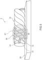
- connection structure of a carbon nanotube wire according to a third embodiment of the present invention will be described using the accompanying drawings hereinafter. Note that since the connection structure of a carbon nanotube wire according to the third embodiment and the connection structures of carbon nanotube wires according to the first and second embodiments share main components, components identical to the components of the connection structures of carbon nanotube wires according to the first and second embodiments will be described using identical reference numerals. Note that FIG. 5 is an explanatory view of an aspect in which a conducting wire is wound around a perimeter of a carbon nanotube wire in which a penetrating part of the conducting wire to be used for the connection structure according to the third embodiment of the present invention is formed.
- connection structure 3 of a carbon nanotube wire As shown in FIG. 5 , in the connection structure 3 of a carbon nanotube wire according to the third embodiment, a penetrating part 31 of the conducting wire 30 and a winding part 32 are formed at a tip portion 13 of the CNT wire 10.
- the connection target of the CNT wire 10 is, for example, a substrate or another CNT wire (substrate 20 in FIG. 5 ) and the tip portion 13 of the CNT wire 10 is soldered to the connection target.
- the winding part 32 is formed at the CNT wire 10, the outer circumference of the CNT wire 10 is held by the winding part 32 and a pressure is applied from the outer circumferential surface, and so it is possible to prevent a reduction in the area of contact between CNTs and prevent a reduction in conductivity.
- the pressure be substantially uniformly applied over the whole surface of the outer circumferential surface of the CNT wire 10 on which the winding part 32 is formed. Examples of the method for applying the pressure over the whole surface of the winding part 32 substantially uniformly include increasing the number of turns of the winding part 32, setting a start point and an end point of the winding part 32 at positions parallel to the longitudinal direction of the CNT wire 10.
- connection structure of a carbon nanotube wire of the present invention will be described hereinafter.
- the connection structure of a carbon nanotube wire in the above-described embodiments is provided with the winding part of the conducting wire, the winding part may not be provided as long as the penetrating part of the conducting wire is formed.
- the connection structure of a carbon nanotube wire in the above-described embodiments is provided with a penetrating part and a winding part using one conducting wire. Instead, however, the connection structure may be provided with a penetrating part and a winding part using a plurality of conducting wires. Therefore, a plurality of penetrating parts of the conducting wire may be provided.
- the plurality of penetrating parts of the conducting wire may also be formed on one cross section having components orthogonal to the longitudinal direction of the CNT wire or the plurality of penetrating parts of the conducting wire may also be formed on a plurality of cross sections having components orthogonal to the longitudinal direction of the CNT wire. Since the plurality of penetrating parts of the conducting wire are formed on one cross section having components orthogonal to the longitudinal direction of the CNT wire, the region of the joint to which solder is applied becomes narrower, and it is possible to form a compact connection structure of a carbon nanotube wire.
- the plurality of penetrating parts of the conducting wire are formed on a plurality of cross sections having components orthogonal to the longitudinal direction of the CNT wire, the region of the joint to which solder is applied is widened, and the joint strength of the joint is further structured.
- connection structure of a carbon nanotube wire in the above-described embodiments, although the conducting wire of the winding part is wound at a predetermined interval in the longitudinal direction of the CNT wire. Instead, however, the conducting wire may be wound without any predetermined interval with the neighboring conducting wires in contact with each other.
- CNTs are created and CNT elemental wires are created from a plurality of CNTs obtained.
- a stranded wire of CNT is created by twisting the plurality of CNT elemental wires obtained.
- the CNT can be created using methods such as a floating catalyst method ( Japanese Patent Publication No. 5819888 ), or a substrate method ( Japanese Patent Publication No. 5590603 ).
- the CNT elemental wire can be created using methods such as dry spinning ( Japanese Patent Publication No. 5819888 , Japanese Patent Publication No. 5990202 , Japanese Patent Publication No. 5350635 ), wet spinning ( Japanese Patent Publication No. 5135620 , Japanese Patent Publication No. 5131571 , Japanese Patent Publication No. 5288359 ), liquid crystal spinning (National Publication of International Patent Application No. 2014-530964 ).
- Two CNT wires (diameter 0.2 mm) were prepared by twisting seven elemental wires of CNT and end portions of the two CNT wires were arranged in parallel.
- One copper wire (diameter 0.025 mm) was prepared as the conducting wire.
- the copper wire was pierced into a region where the two CNT wires were arranged in parallel and a penetrating part of the copper wire was formed in the two CNT wires.
- the perimeters of the two CNT wires were wound with the copper wire in which the penetrating part was formed so as to bundle the two CNT wires, a winding part was thereby formed and a connection structure was created.
- a width of the winding part was set to 1 mm.
- connection structure was created using a method similar to the method in Example 1 except in that two copper wires were used as the conducting wire instead of the one copper wire and the two copper wires were pierced into the cross section orthogonal to the longitudinal direction of the CNT wire so that the two copper wires were substantially orthogonal.
- connection structure was created using a method similar to the method in Example 1 except in that a copper wire having a diameter of 0.080 mm was used instead of the copper wire having a diameter of 0.025 mm.
- connection structure was created using a method similar to the method in Example 3 except in that two copper wires were used instead of one copper wire and the two copper wires were pierced into the cross section orthogonal to the longitudinal direction of the CNT wire so that the two copper wires were substantially orthogonal.
- connection structure was created using a method similar to the method in Example 1 except in that a copper wire having a diameter of 0.250 mm was used instead of the copper wire having a diameter of 0.025 mm.
- connection structure was created using a method similar to the method in Example 5 except in that two copper wires were used instead of one copper wire and the two copper wires were pierced into the cross section orthogonal to the longitudinal direction of the CNT wire so that the two copper wires were substantially orthogonal.
- solder was applied to the penetrating part and the winding part to connect the two CNT wires, the CNT wires were linearly lengthened, and a sample of the connection structure of a carbon nanotube wire of the present invention was created.
- lead-based solder was used as the solder.
- one unconnected CNT wire CNT wire (diameter 0.2 mm) obtained by twisting seven elemental wires of CNT) was used.
- Evaluation items and evaluation methods are as follows:
- a ratio of a cross-sectional area in radial direction of a conducting wire to a cross-sectional area in radial direction of a carbon nanotube wire in the penetrating part of the connection structure of a carbon nanotube wire was calculated by extracting the cross section of the connection structure of a carbon nanotube wire and calculating the cross-sectional area in radial direction of the conducting wire in the penetrating part/the cross-sectional area in radial direction of the CNT wire based on a SEM-acquired image.
- a resistance value of the connection structure of a carbon nanotube wire was measured by connecting the connection structure of a carbon nanotube wire to a low voltage source meter (manufactured by Keithley Instruments & Products, apparatus name “2401 SourceMeter”) and a digital multimeter (manufactured by Keithley Instruments & Products, apparatus name “2000 multimeter”) and using a four-terminal method.
- a tester grasped and pulled both end portions of a sample of the connection structure of a carbon nanotube wire and visually observed a connection situation of the sample.
- Examples 1 to 6 which are connection structures in which two CNT wires are connected by solder all show that the resistance values can be reduced to the same level as the resistance value of one CNT wire and demonstrate excellent electrical connectivity.
- Example 1 to 6 also show that tensile strength is also good, mechanical connectivity is also excellent, and especially in Examples 2 to 6 in which the ratio of the cross-sectional area of the copper wire to the cross-sectional area of the carbon nanotube is 10% or more, mechanical connectivity is further excellent. Furthermore, in Examples 4 to 6 in which the ratio of the copper wire is 30% or more, a significant reduction in resistance value has been observed.
Landscapes
- Chemical & Material Sciences (AREA)
- Engineering & Computer Science (AREA)
- Materials Engineering (AREA)
- Nanotechnology (AREA)
- Organic Chemistry (AREA)
- Chemical Kinetics & Catalysis (AREA)
- General Chemical & Material Sciences (AREA)
- Textile Engineering (AREA)
- Inorganic Chemistry (AREA)
- Carbon And Carbon Compounds (AREA)
- Non-Insulated Conductors (AREA)
Applications Claiming Priority (2)
| Application Number | Priority Date | Filing Date | Title |
|---|---|---|---|
| JP2020065007 | 2020-03-31 | ||
| PCT/JP2021/013829 WO2021201096A1 (ja) | 2020-03-31 | 2021-03-31 | カーボンナノチューブ線材の接続構造体 |
Publications (2)
| Publication Number | Publication Date |
|---|---|
| EP4131289A1 true EP4131289A1 (de) | 2023-02-08 |
| EP4131289A4 EP4131289A4 (de) | 2024-04-10 |
Family
ID=77927899
Family Applications (1)
| Application Number | Title | Priority Date | Filing Date |
|---|---|---|---|
| EP21780030.9A Withdrawn EP4131289A4 (de) | 2020-03-31 | 2021-03-31 | Verbindungsstruktur für kohlenstoffnanoröhrchendraht |
Country Status (5)
| Country | Link |
|---|---|
| US (1) | US12362077B2 (de) |
| EP (1) | EP4131289A4 (de) |
| JP (1) | JP7598926B2 (de) |
| CN (1) | CN115349153B (de) |
| WO (1) | WO2021201096A1 (de) |
Families Citing this family (1)
| Publication number | Priority date | Publication date | Assignee | Title |
|---|---|---|---|---|
| CN120496927A (zh) * | 2025-06-12 | 2025-08-15 | 南京全信传输科技股份有限公司 | 一种碳纳米管导体轻量化柔软电线线缆 |
Family Cites Families (37)
| Publication number | Priority date | Publication date | Assignee | Title |
|---|---|---|---|---|
| SE0001123L (sv) * | 2000-03-30 | 2001-10-01 | Abb Ab | Kraftkabel |
| GB0316367D0 (en) | 2003-07-11 | 2003-08-13 | Univ Cambridge Tech | Production of agglomerates from gas phase |
| JP4333285B2 (ja) * | 2003-09-01 | 2009-09-16 | Jfeエンジニアリング株式会社 | カーボンナノチューブの基材へのろう付け方法 |
| US7956287B2 (en) * | 2004-04-20 | 2011-06-07 | Takiron Co., Ltd. | Transparent conductive formed article for a touch panel and touch panel |
| CN105696138B (zh) | 2004-11-09 | 2019-02-01 | 得克萨斯大学体系董事会 | 纳米纤维纱线、带和板的制造和应用 |
| AU2006240013A1 (en) * | 2005-04-22 | 2006-11-02 | The Regents Of The University Of California | Nanotubes as microwave frequency interconnects |
| US8013247B2 (en) * | 2006-04-25 | 2011-09-06 | The Mitre Corporation | Carbon nanotube-based electronic devices |
| CN101086939B (zh) * | 2006-06-09 | 2010-05-12 | 清华大学 | 场发射元件及其制备方法 |
| CN101286385B (zh) * | 2007-04-11 | 2010-05-26 | 清华大学 | 电磁屏蔽线缆 |
| CN105244071B (zh) * | 2008-02-01 | 2018-11-30 | 北京富纳特创新科技有限公司 | 线缆 |
| US20120177926A1 (en) * | 2008-05-07 | 2012-07-12 | Nanocomp Technologies, Inc. | Nanostructure composite sheets and methods of use |
| MX2008013821A (es) * | 2008-10-28 | 2010-04-28 | Magnekon S A De C V | Alambre magneto con revestimiento adicionado con nanoestructuras tipo fulereno. |
| US8445788B1 (en) * | 2009-01-05 | 2013-05-21 | The Boeing Company | Carbon nanotube-enhanced, metallic wire |
| US9111658B2 (en) * | 2009-04-24 | 2015-08-18 | Applied Nanostructured Solutions, Llc | CNS-shielded wires |
| WO2010148157A1 (en) * | 2009-06-19 | 2010-12-23 | 3M Innovative Properties Company | Shielded electrical cable and method of making |
| US8354593B2 (en) * | 2009-07-10 | 2013-01-15 | Nanocomp Technologies, Inc. | Hybrid conductors and method of making same |
| JP5590603B2 (ja) | 2010-04-09 | 2014-09-17 | 日本ゼオン株式会社 | カーボンナノチューブ配向集合体の製造装置 |
| CN102063959B (zh) * | 2010-11-18 | 2013-02-13 | 清华大学 | 线缆 |
| JP5131571B2 (ja) | 2010-11-22 | 2013-01-30 | 古河電気工業株式会社 | 凝集紡糸構造体の製造方法および凝集紡糸構造体 |
| JP5135620B2 (ja) | 2010-11-22 | 2013-02-06 | 古河電気工業株式会社 | 凝集紡糸構造体および電線 |
| WO2012070537A1 (ja) | 2010-11-22 | 2012-05-31 | 古河電気工業株式会社 | 凝集紡糸構造体およびその製造方法ならびにそれを用いた電線 |
| US20140084219A1 (en) | 2011-02-28 | 2014-03-27 | William Marsh Rice University | Doped multiwalled carbon nanotube fibers and methods of making the same |
| US20130048337A1 (en) * | 2011-08-24 | 2013-02-28 | Tyco Electronics Corporation | Carbon-based substrates with organometallic fillers |
| JP5786564B2 (ja) * | 2011-08-29 | 2015-09-30 | 株式会社デンソー | カーボンナノチューブ糸接続体及びその製造方法 |
| WO2013034672A2 (en) | 2011-09-07 | 2013-03-14 | Teijin Aramid B.V. | Carbon nanotubes fiber having low resistivity |
| EP2817806A1 (de) * | 2012-02-22 | 2014-12-31 | Seldon Technologies, Inc. | Elektroden und anwendungen davon |
| US20140046291A1 (en) | 2012-04-26 | 2014-02-13 | Evena Medical, Inc. | Vein imaging systems and methods |
| US20140039309A1 (en) | 2012-04-26 | 2014-02-06 | Evena Medical, Inc. | Vein imaging systems and methods |
| US9685258B2 (en) * | 2012-11-09 | 2017-06-20 | Northrop Grumman Systems Corporation | Hybrid carbon nanotube shielding for lightweight electrical cables |
| US9293233B2 (en) * | 2013-02-11 | 2016-03-22 | Tyco Electronics Corporation | Composite cable |
| JP6738627B2 (ja) * | 2016-03-24 | 2020-08-12 | 古河電気工業株式会社 | カーボンナノチューブ線材及びカーボンナノチューブ線材接続構造体 |
| JP6767292B2 (ja) * | 2016-03-24 | 2020-10-14 | 古河電気工業株式会社 | カーボンナノチューブ線材及びカーボンナノチューブ線材接続構造体 |
| JP2017174689A (ja) * | 2016-03-24 | 2017-09-28 | 古河電気工業株式会社 | カーボンナノチューブ線材及びカーボンナノチューブ線材接続構造体 |
| JP6719244B2 (ja) * | 2016-03-24 | 2020-07-08 | 古河電気工業株式会社 | カーボンナノチューブ線材の接続方法及びカーボンナノチューブ線材接続構造体 |
| US10109391B2 (en) * | 2017-02-20 | 2018-10-23 | Delphi Technologies, Inc. | Metallic/carbon nanotube composite wire |
| JP7097165B2 (ja) * | 2017-10-03 | 2022-07-07 | 古河電気工業株式会社 | カーボンナノチューブ線材、カーボンナノチューブ線材接続構造体及びカーボンナノチューブ線材の製造方法 |
| JP6928526B2 (ja) * | 2017-10-03 | 2021-09-01 | 古河電気工業株式会社 | カーボンナノチューブ線材、カーボンナノチューブ線材接続構造体及びカーボンナノチューブ線材の製造方法 |
-
2021
- 2021-03-31 WO PCT/JP2021/013829 patent/WO2021201096A1/ja not_active Ceased
- 2021-03-31 JP JP2022512619A patent/JP7598926B2/ja active Active
- 2021-03-31 CN CN202180025938.7A patent/CN115349153B/zh active Active
- 2021-03-31 EP EP21780030.9A patent/EP4131289A4/de not_active Withdrawn
-
2022
- 2022-09-20 US US17/933,752 patent/US12362077B2/en active Active
Also Published As
| Publication number | Publication date |
|---|---|
| US20230014073A1 (en) | 2023-01-19 |
| CN115349153A (zh) | 2022-11-15 |
| EP4131289A4 (de) | 2024-04-10 |
| JP7598926B2 (ja) | 2024-12-12 |
| US12362077B2 (en) | 2025-07-15 |
| WO2021201096A1 (ja) | 2021-10-07 |
| JPWO2021201096A1 (de) | 2021-10-07 |
| CN115349153B (zh) | 2025-04-25 |
Similar Documents
| Publication | Publication Date | Title |
|---|---|---|
| KR102005669B1 (ko) | 금속/카본 나노튜브 복합 와이어 | |
| EP2192601B1 (de) | Kabelbaum und verfahren zu seiner herstellung | |
| DE112016000034T5 (de) | Supratleitender Draht und Verfahren zu seiner Herstellung | |
| WO2019086619A1 (de) | Diodenlaser | |
| US12362077B2 (en) | Connection structure of carbon nanotube wire | |
| DE102015105573A1 (de) | Prüfsonde und Verfahren zum Herstellen einer Prüfsonde | |
| DE102012018387A1 (de) | Textiler thermoelektrischer Generator | |
| US20090184107A1 (en) | Heating element with stranded contact | |
| EP3155387A1 (de) | Temperatursensor, insbesondere hochtemperatursensor, abgastemperaturüberwachungssystem und verfahren zur herstellung des temperatursensors | |
| CN113646254B (zh) | 基板与碳纳米管线材的连接结构体 | |
| WO2008080467A1 (de) | Anschlussdraht, verfahren zur herstellung eines solchen und baugruppe | |
| WO2008025547A1 (de) | Aluminium aufweisende bonddrähte mit eingebetteten kupferfasern | |
| DE102006025661B4 (de) | Kontaktklemme zum Anschließen eines Litzenleiters an einen relativ dünnen Anschlussstift | |
| DE19827542A1 (de) | Hochtemperaturfeste Kontaktvorrichtung zur Kontaktierung eines planaren Sensorelements | |
| JP4462004B2 (ja) | 複合導体及びその製造方法並びにそれを用いたケーブル | |
| JPH0433272A (ja) | 超電導線の接続方法 | |
| DE102023124584A1 (de) | Sensoranordnung und Verfahren zur Herstellung einer Sensoranordnung | |
| DE60019515T2 (de) | Elektrische lampe | |
| WO2025040722A1 (de) | Sensorbaugruppe und verfahren zur herstellung einer sensorbaugruppe | |
| DE54441C (de) | Elektrische Stromleitung | |
| EP0182068A2 (de) | Oberflächenmontagekondensator | |
| DE202006008713U1 (de) | Kontaktklemme zum Anschließen eines Litzenleiters an einen relativ dünnen Anschlussstift | |
| DE212019000435U1 (de) | Heizeinrichtung und mit Heizeinrichtung ausgestattete Glühkerze | |
| DE20114622U1 (de) | Heizelement mit Litzen-Kontakt | |
| JP2000231948A (ja) | 超電導線の接続方法 |
Legal Events
| Date | Code | Title | Description |
|---|---|---|---|
| STAA | Information on the status of an ep patent application or granted ep patent |
Free format text: STATUS: THE INTERNATIONAL PUBLICATION HAS BEEN MADE |
|
| PUAI | Public reference made under article 153(3) epc to a published international application that has entered the european phase |
Free format text: ORIGINAL CODE: 0009012 |
|
| STAA | Information on the status of an ep patent application or granted ep patent |
Free format text: STATUS: REQUEST FOR EXAMINATION WAS MADE |
|
| 17P | Request for examination filed |
Effective date: 20221012 |
|
| AK | Designated contracting states |
Kind code of ref document: A1 Designated state(s): AL AT BE BG CH CY CZ DE DK EE ES FI FR GB GR HR HU IE IS IT LI LT LU LV MC MK MT NL NO PL PT RO RS SE SI SK SM TR |
|
| DAV | Request for validation of the european patent (deleted) | ||
| DAX | Request for extension of the european patent (deleted) | ||
| REG | Reference to a national code |
Ref country code: DE Ref legal event code: R079 Free format text: PREVIOUS MAIN CLASS: H01B0005080000 Ipc: C01B0032168000 |
|
| A4 | Supplementary search report drawn up and despatched |
Effective date: 20240312 |
|
| RIC1 | Information provided on ipc code assigned before grant |
Ipc: H01R 13/02 20060101ALN20240305BHEP Ipc: D01F 9/12 20060101ALI20240305BHEP Ipc: H01R 12/53 20110101ALI20240305BHEP Ipc: H01R 4/02 20060101ALI20240305BHEP Ipc: C01B 32/168 20170101AFI20240305BHEP |
|
| GRAP | Despatch of communication of intention to grant a patent |
Free format text: ORIGINAL CODE: EPIDOSNIGR1 |
|
| STAA | Information on the status of an ep patent application or granted ep patent |
Free format text: STATUS: GRANT OF PATENT IS INTENDED |
|
| RIC1 | Information provided on ipc code assigned before grant |
Ipc: H01R 13/02 20060101ALN20241217BHEP Ipc: D01F 9/12 20060101ALI20241217BHEP Ipc: H01R 12/53 20110101ALI20241217BHEP Ipc: H01R 4/02 20060101ALI20241217BHEP Ipc: C01B 32/168 20170101AFI20241217BHEP |
|
| INTG | Intention to grant announced |
Effective date: 20250115 |
|
| STAA | Information on the status of an ep patent application or granted ep patent |
Free format text: STATUS: THE APPLICATION IS DEEMED TO BE WITHDRAWN |
|
| 18D | Application deemed to be withdrawn |
Effective date: 20250516 |