EP4068374B1 - Anzeigesubstrat und anzeigevorrichtung - Google Patents
Anzeigesubstrat und anzeigevorrichtung Download PDFInfo
- Publication number
- EP4068374B1 EP4068374B1 EP19945420.8A EP19945420A EP4068374B1 EP 4068374 B1 EP4068374 B1 EP 4068374B1 EP 19945420 A EP19945420 A EP 19945420A EP 4068374 B1 EP4068374 B1 EP 4068374B1
- Authority
- EP
- European Patent Office
- Prior art keywords
- sub
- pixel
- circuit
- electrode
- terminal
- Prior art date
- Legal status (The legal status is an assumption and is not a legal conclusion. Google has not performed a legal analysis and makes no representation as to the accuracy of the status listed.)
- Active
Links
Images


Classifications
-
- G—PHYSICS
- G09—EDUCATION; CRYPTOGRAPHY; DISPLAY; ADVERTISING; SEALS
- G09G—ARRANGEMENTS OR CIRCUITS FOR CONTROL OF INDICATING DEVICES USING STATIC MEANS TO PRESENT VARIABLE INFORMATION
- G09G3/00—Control arrangements or circuits, of interest only in connection with visual indicators other than cathode-ray tubes
- G09G3/20—Control arrangements or circuits, of interest only in connection with visual indicators other than cathode-ray tubes for presentation of an assembly of a number of characters, e.g. a page, by composing the assembly by combination of individual elements arranged in a matrix no fixed position being assigned to or needed to be assigned to the individual characters or partial characters
- G09G3/22—Control arrangements or circuits, of interest only in connection with visual indicators other than cathode-ray tubes for presentation of an assembly of a number of characters, e.g. a page, by composing the assembly by combination of individual elements arranged in a matrix no fixed position being assigned to or needed to be assigned to the individual characters or partial characters using controlled light sources
- G09G3/30—Control arrangements or circuits, of interest only in connection with visual indicators other than cathode-ray tubes for presentation of an assembly of a number of characters, e.g. a page, by composing the assembly by combination of individual elements arranged in a matrix no fixed position being assigned to or needed to be assigned to the individual characters or partial characters using controlled light sources using electroluminescent panels
- G09G3/32—Control arrangements or circuits, of interest only in connection with visual indicators other than cathode-ray tubes for presentation of an assembly of a number of characters, e.g. a page, by composing the assembly by combination of individual elements arranged in a matrix no fixed position being assigned to or needed to be assigned to the individual characters or partial characters using controlled light sources using electroluminescent panels semiconductive, e.g. using light-emitting diodes [LED]
- G09G3/3208—Control arrangements or circuits, of interest only in connection with visual indicators other than cathode-ray tubes for presentation of an assembly of a number of characters, e.g. a page, by composing the assembly by combination of individual elements arranged in a matrix no fixed position being assigned to or needed to be assigned to the individual characters or partial characters using controlled light sources using electroluminescent panels semiconductive, e.g. using light-emitting diodes [LED] organic, e.g. using organic light-emitting diodes [OLED]
- G09G3/3225—Control arrangements or circuits, of interest only in connection with visual indicators other than cathode-ray tubes for presentation of an assembly of a number of characters, e.g. a page, by composing the assembly by combination of individual elements arranged in a matrix no fixed position being assigned to or needed to be assigned to the individual characters or partial characters using controlled light sources using electroluminescent panels semiconductive, e.g. using light-emitting diodes [LED] organic, e.g. using organic light-emitting diodes [OLED] using an active matrix
- G09G3/3233—Control arrangements or circuits, of interest only in connection with visual indicators other than cathode-ray tubes for presentation of an assembly of a number of characters, e.g. a page, by composing the assembly by combination of individual elements arranged in a matrix no fixed position being assigned to or needed to be assigned to the individual characters or partial characters using controlled light sources using electroluminescent panels semiconductive, e.g. using light-emitting diodes [LED] organic, e.g. using organic light-emitting diodes [OLED] using an active matrix with pixel circuitry controlling the current through the light-emitting element
-
- G—PHYSICS
- G09—EDUCATION; CRYPTOGRAPHY; DISPLAY; ADVERTISING; SEALS
- G09G—ARRANGEMENTS OR CIRCUITS FOR CONTROL OF INDICATING DEVICES USING STATIC MEANS TO PRESENT VARIABLE INFORMATION
- G09G3/00—Control arrangements or circuits, of interest only in connection with visual indicators other than cathode-ray tubes
- G09G3/20—Control arrangements or circuits, of interest only in connection with visual indicators other than cathode-ray tubes for presentation of an assembly of a number of characters, e.g. a page, by composing the assembly by combination of individual elements arranged in a matrix no fixed position being assigned to or needed to be assigned to the individual characters or partial characters
- G09G3/22—Control arrangements or circuits, of interest only in connection with visual indicators other than cathode-ray tubes for presentation of an assembly of a number of characters, e.g. a page, by composing the assembly by combination of individual elements arranged in a matrix no fixed position being assigned to or needed to be assigned to the individual characters or partial characters using controlled light sources
- G09G3/30—Control arrangements or circuits, of interest only in connection with visual indicators other than cathode-ray tubes for presentation of an assembly of a number of characters, e.g. a page, by composing the assembly by combination of individual elements arranged in a matrix no fixed position being assigned to or needed to be assigned to the individual characters or partial characters using controlled light sources using electroluminescent panels
- G09G3/32—Control arrangements or circuits, of interest only in connection with visual indicators other than cathode-ray tubes for presentation of an assembly of a number of characters, e.g. a page, by composing the assembly by combination of individual elements arranged in a matrix no fixed position being assigned to or needed to be assigned to the individual characters or partial characters using controlled light sources using electroluminescent panels semiconductive, e.g. using light-emitting diodes [LED]
- G09G3/3208—Control arrangements or circuits, of interest only in connection with visual indicators other than cathode-ray tubes for presentation of an assembly of a number of characters, e.g. a page, by composing the assembly by combination of individual elements arranged in a matrix no fixed position being assigned to or needed to be assigned to the individual characters or partial characters using controlled light sources using electroluminescent panels semiconductive, e.g. using light-emitting diodes [LED] organic, e.g. using organic light-emitting diodes [OLED]
- G09G3/3266—Details of drivers for scan electrodes
-
- G—PHYSICS
- G09—EDUCATION; CRYPTOGRAPHY; DISPLAY; ADVERTISING; SEALS
- G09G—ARRANGEMENTS OR CIRCUITS FOR CONTROL OF INDICATING DEVICES USING STATIC MEANS TO PRESENT VARIABLE INFORMATION
- G09G3/00—Control arrangements or circuits, of interest only in connection with visual indicators other than cathode-ray tubes
- G09G3/20—Control arrangements or circuits, of interest only in connection with visual indicators other than cathode-ray tubes for presentation of an assembly of a number of characters, e.g. a page, by composing the assembly by combination of individual elements arranged in a matrix no fixed position being assigned to or needed to be assigned to the individual characters or partial characters
- G09G3/22—Control arrangements or circuits, of interest only in connection with visual indicators other than cathode-ray tubes for presentation of an assembly of a number of characters, e.g. a page, by composing the assembly by combination of individual elements arranged in a matrix no fixed position being assigned to or needed to be assigned to the individual characters or partial characters using controlled light sources
- G09G3/30—Control arrangements or circuits, of interest only in connection with visual indicators other than cathode-ray tubes for presentation of an assembly of a number of characters, e.g. a page, by composing the assembly by combination of individual elements arranged in a matrix no fixed position being assigned to or needed to be assigned to the individual characters or partial characters using controlled light sources using electroluminescent panels
- G09G3/32—Control arrangements or circuits, of interest only in connection with visual indicators other than cathode-ray tubes for presentation of an assembly of a number of characters, e.g. a page, by composing the assembly by combination of individual elements arranged in a matrix no fixed position being assigned to or needed to be assigned to the individual characters or partial characters using controlled light sources using electroluminescent panels semiconductive, e.g. using light-emitting diodes [LED]
- G09G3/3208—Control arrangements or circuits, of interest only in connection with visual indicators other than cathode-ray tubes for presentation of an assembly of a number of characters, e.g. a page, by composing the assembly by combination of individual elements arranged in a matrix no fixed position being assigned to or needed to be assigned to the individual characters or partial characters using controlled light sources using electroluminescent panels semiconductive, e.g. using light-emitting diodes [LED] organic, e.g. using organic light-emitting diodes [OLED]
- G09G3/3275—Details of drivers for data electrodes
-
- H—ELECTRICITY
- H10—SEMICONDUCTOR DEVICES; ELECTRIC SOLID-STATE DEVICES NOT OTHERWISE PROVIDED FOR
- H10D—INORGANIC ELECTRIC SEMICONDUCTOR DEVICES
- H10D86/00—Integrated devices formed in or on insulating or conducting substrates, e.g. formed in silicon-on-insulator [SOI] substrates or on stainless steel or glass substrates
- H10D86/40—Integrated devices formed in or on insulating or conducting substrates, e.g. formed in silicon-on-insulator [SOI] substrates or on stainless steel or glass substrates characterised by multiple TFTs
- H10D86/481—Integrated devices formed in or on insulating or conducting substrates, e.g. formed in silicon-on-insulator [SOI] substrates or on stainless steel or glass substrates characterised by multiple TFTs integrated with passive devices, e.g. auxiliary capacitors
-
- H—ELECTRICITY
- H10—SEMICONDUCTOR DEVICES; ELECTRIC SOLID-STATE DEVICES NOT OTHERWISE PROVIDED FOR
- H10D—INORGANIC ELECTRIC SEMICONDUCTOR DEVICES
- H10D86/00—Integrated devices formed in or on insulating or conducting substrates, e.g. formed in silicon-on-insulator [SOI] substrates or on stainless steel or glass substrates
- H10D86/40—Integrated devices formed in or on insulating or conducting substrates, e.g. formed in silicon-on-insulator [SOI] substrates or on stainless steel or glass substrates characterised by multiple TFTs
- H10D86/60—Integrated devices formed in or on insulating or conducting substrates, e.g. formed in silicon-on-insulator [SOI] substrates or on stainless steel or glass substrates characterised by multiple TFTs wherein the TFTs are in active matrices
-
- H—ELECTRICITY
- H10—SEMICONDUCTOR DEVICES; ELECTRIC SOLID-STATE DEVICES NOT OTHERWISE PROVIDED FOR
- H10K—ORGANIC ELECTRIC SOLID-STATE DEVICES
- H10K59/00—Integrated devices, or assemblies of multiple devices, comprising at least one organic light-emitting element covered by group H10K50/00
- H10K59/10—OLED displays
- H10K59/12—Active-matrix OLED [AMOLED] displays
- H10K59/121—Active-matrix OLED [AMOLED] displays characterised by the geometry or disposition of pixel elements
-
- H—ELECTRICITY
- H10—SEMICONDUCTOR DEVICES; ELECTRIC SOLID-STATE DEVICES NOT OTHERWISE PROVIDED FOR
- H10K—ORGANIC ELECTRIC SOLID-STATE DEVICES
- H10K59/00—Integrated devices, or assemblies of multiple devices, comprising at least one organic light-emitting element covered by group H10K50/00
- H10K59/10—OLED displays
- H10K59/12—Active-matrix OLED [AMOLED] displays
- H10K59/131—Interconnections, e.g. wiring lines or terminals
-
- H—ELECTRICITY
- H10—SEMICONDUCTOR DEVICES; ELECTRIC SOLID-STATE DEVICES NOT OTHERWISE PROVIDED FOR
- H10K—ORGANIC ELECTRIC SOLID-STATE DEVICES
- H10K59/00—Integrated devices, or assemblies of multiple devices, comprising at least one organic light-emitting element covered by group H10K50/00
- H10K59/30—Devices specially adapted for multicolour light emission
- H10K59/35—Devices specially adapted for multicolour light emission comprising red-green-blue [RGB] subpixels
- H10K59/353—Devices specially adapted for multicolour light emission comprising red-green-blue [RGB] subpixels characterised by the geometrical arrangement of the RGB subpixels
-
- G—PHYSICS
- G09—EDUCATION; CRYPTOGRAPHY; DISPLAY; ADVERTISING; SEALS
- G09G—ARRANGEMENTS OR CIRCUITS FOR CONTROL OF INDICATING DEVICES USING STATIC MEANS TO PRESENT VARIABLE INFORMATION
- G09G2300/00—Aspects of the constitution of display devices
- G09G2300/04—Structural and physical details of display devices
- G09G2300/0421—Structural details of the set of electrodes
- G09G2300/0426—Layout of electrodes and connections
-
- G—PHYSICS
- G09—EDUCATION; CRYPTOGRAPHY; DISPLAY; ADVERTISING; SEALS
- G09G—ARRANGEMENTS OR CIRCUITS FOR CONTROL OF INDICATING DEVICES USING STATIC MEANS TO PRESENT VARIABLE INFORMATION
- G09G2300/00—Aspects of the constitution of display devices
- G09G2300/04—Structural and physical details of display devices
- G09G2300/0421—Structural details of the set of electrodes
- G09G2300/043—Compensation electrodes or other additional electrodes in matrix displays related to distortions or compensation signals, e.g. for modifying TFT threshold voltage in column driver
-
- G—PHYSICS
- G09—EDUCATION; CRYPTOGRAPHY; DISPLAY; ADVERTISING; SEALS
- G09G—ARRANGEMENTS OR CIRCUITS FOR CONTROL OF INDICATING DEVICES USING STATIC MEANS TO PRESENT VARIABLE INFORMATION
- G09G2300/00—Aspects of the constitution of display devices
- G09G2300/08—Active matrix structure, i.e. with use of active elements, inclusive of non-linear two terminal elements, in the pixels together with light emitting or modulating elements
- G09G2300/0809—Several active elements per pixel in active matrix panels
- G09G2300/0819—Several active elements per pixel in active matrix panels used for counteracting undesired variations, e.g. feedback or autozeroing
-
- G—PHYSICS
- G09—EDUCATION; CRYPTOGRAPHY; DISPLAY; ADVERTISING; SEALS
- G09G—ARRANGEMENTS OR CIRCUITS FOR CONTROL OF INDICATING DEVICES USING STATIC MEANS TO PRESENT VARIABLE INFORMATION
- G09G2300/00—Aspects of the constitution of display devices
- G09G2300/08—Active matrix structure, i.e. with use of active elements, inclusive of non-linear two terminal elements, in the pixels together with light emitting or modulating elements
- G09G2300/0809—Several active elements per pixel in active matrix panels
- G09G2300/0842—Several active elements per pixel in active matrix panels forming a memory circuit, e.g. a dynamic memory with one capacitor
- G09G2300/0861—Several active elements per pixel in active matrix panels forming a memory circuit, e.g. a dynamic memory with one capacitor with additional control of the display period without amending the charge stored in a pixel memory, e.g. by means of additional select electrodes
-
- H—ELECTRICITY
- H10—SEMICONDUCTOR DEVICES; ELECTRIC SOLID-STATE DEVICES NOT OTHERWISE PROVIDED FOR
- H10K—ORGANIC ELECTRIC SOLID-STATE DEVICES
- H10K59/00—Integrated devices, or assemblies of multiple devices, comprising at least one organic light-emitting element covered by group H10K50/00
- H10K59/10—OLED displays
- H10K59/12—Active-matrix OLED [AMOLED] displays
- H10K59/121—Active-matrix OLED [AMOLED] displays characterised by the geometry or disposition of pixel elements
- H10K59/1213—Active-matrix OLED [AMOLED] displays characterised by the geometry or disposition of pixel elements the pixel elements being TFTs
-
- H—ELECTRICITY
- H10—SEMICONDUCTOR DEVICES; ELECTRIC SOLID-STATE DEVICES NOT OTHERWISE PROVIDED FOR
- H10K—ORGANIC ELECTRIC SOLID-STATE DEVICES
- H10K59/00—Integrated devices, or assemblies of multiple devices, comprising at least one organic light-emitting element covered by group H10K50/00
- H10K59/10—OLED displays
- H10K59/12—Active-matrix OLED [AMOLED] displays
- H10K59/121—Active-matrix OLED [AMOLED] displays characterised by the geometry or disposition of pixel elements
- H10K59/1216—Active-matrix OLED [AMOLED] displays characterised by the geometry or disposition of pixel elements the pixel elements being capacitors
-
- H—ELECTRICITY
- H10—SEMICONDUCTOR DEVICES; ELECTRIC SOLID-STATE DEVICES NOT OTHERWISE PROVIDED FOR
- H10K—ORGANIC ELECTRIC SOLID-STATE DEVICES
- H10K59/00—Integrated devices, or assemblies of multiple devices, comprising at least one organic light-emitting element covered by group H10K50/00
- H10K59/10—OLED displays
- H10K59/12—Active-matrix OLED [AMOLED] displays
- H10K59/123—Connection of the pixel electrodes to the thin film transistors [TFT]
Definitions
- US2019/131371 A1 discloses a display apparatus including a first thin film transistor (TFT) disposed in a first pixel region and including a first semiconductor layer and a first gate electrode, where the semiconductor layer includes first source and drain regions; a second TFT disposed in a second pixel region adjacent the first pixel region and including a second semiconductor layer and a second gate electrode, where the second semiconductor layer includes a second source and drain regions; a first pixel electrode disposed in the first pixel region and including a first region where a first light-emitting layer is disposed and a second region extending from the first region; and a second pixel electrode disposed in the second pixel region and including a third region where a second light-emitting layer is disposed and a fourth region extending from the third region and disposed on
- TFT thin film transistor
- US2016/225838A1 discloses an organic light emitting diode display including a plurality of pixels including a first pixel, a second pixel, and a third pixel connected to the plurality of scan lines and the plurality of data lines, wherein each pixel includes a switching transistor connected to the scan line and the data line, a driving transistor connected to the switching transistor, an organic light emitting diode connected to the driving transistor, and a light emission control transistor between the driving transistor and the organic light emitting diode and configured to be turned on by the light emission control signal.
- CN110265458A discloses an array substrate comprising a plurality of pixel units arranged in an array, light-emitting elements, and a plurality of first wires.
- connection is not intended to define a physical connection or mechanical connection, but may include an electrical connection, directly or indirectly.
- "On,” “under,” “right,” “left” and the like are only used to indicate relative position relationship, and when the position of the object which is described is changed, the relative position relationship may be changed accordingly.
- OLED Organic Light Emitting Diode
- a display substrate such as the arrangement of pixels and signal lines.
- OLED display device with a resolution of 4K due to its doubled sub-pixel units, the OLED display device with a large size and a resolution of 8K has a doubled pixel density.
- a line width of a signal line is decreased, which leads to an increased self-resistance of the signal line; and on the other hand, overlap of signal lines occurs often, causing an increased parasitic capacitance of the signal line, which all leads to an increased resistance-capacitance load of the signal line.
- signal delay (RC delay), voltage drop (IR drop), voltage rise (IR rise), or the like caused by the resistance-capacitance load may become serious. These phenomena may seriously affect display quality of a display product.
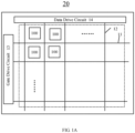
- Fig. 1A is a block diagram of a display substrate according to at least one embodiment of the disclosure.
- the display substrate 20 includes a plurality of sub-pixels 100, a plurality of gate lines 11, and a plurality of data lines 12 arranged in an array.
- Each sub-pixel 100 includes a light emitting element and a pixel circuit driving the light emitting element.
- the plurality of gate lines 11 and the plurality of data lines 12 intersect with one another to define a plurality of pixel regions arranged in an array in the display region, and a pixel circuit of one sub-pixel 100 is disposed in each pixel region.
- the pixel circuit is, for example, a conventional pixel circuit, such as a 2T1C (i.e., two transistors and one capacitor) pixel circuit, nTmC (n, m are positive integers) pixel circuit, such as 4T2C, 5T1C, 7T1C, etc., and in various embodiments, the pixel circuit may further include a compensation sub-circuit that includes an internal compensation sub-circuit or an external compensation sub-circuit, which may include transistors, capacitors, etc..
- the pixel circuit may further include a reset circuit, a light emission control sub-circuit, a detection circuit, or the like as necessary.
- the display substrate may further include a gate drive sub-circuit 13 and a data drive sub-circuit 14 in a non-display region.
- the gate drive sub-circuit 13 is connected to the pixel circuit through the gate line 11 to provide various scanning signals
- the data drive sub-circuit 14 is connected to the pixel circuit through the data line 12 to provide data signals.
- the positions of the gate drive sub-circuit 13 and the data drive sub-circuit 14 as well as the gate lines 11 and the data lines 12 in the display substrate shown in Fig. 1A are merely examples, and may be designed as required actually.
- the display substrate 20 may further include a control circuit (not shown).
- the control circuit is configured to control the data drive sub-circuit 14 to apply the data signal, and to control the gate electrode drive sub-circuit to apply the scanning signal.
- One example of the control circuit is a timing control circuit (T-con).
- the control circuit may be in various forms, for example including a processor and a memory, the memory including executable codes that the processor may execute to perform the above-mentioned detection method.
- the processor may be a Central Processing Unit (CPU) or other form of processing device having data processing capabilities and/or instruction execution capabilities, and may include, for example, a microprocessor, a Programmable Logic Controller (PLC), or the like.
- CPU Central Processing Unit
- PLC Programmable Logic Controller
- a storage device may include one or more computer program products that may include various forms of computer-readable storage media, such as volatile memory and/or non-volatile memory.
- the volatile memory may include, for example, a random access memory (RAM), and/or a cache memory (cache), or the like.
- the non-volatile memory may include, for example, a read only memory (ROM), a hard disk, a flash memory, etc..
- One or more computer program instructions may be stored on a computer-readable storage medium and the processor may perform the function desired by the program instruction.
- Various applications and data may also be stored in the computer-readable storage medium.
- the pixel circuit may include a drive sub-circuit, a data write sub-circuit, a compensation sub-circuit, and a storage sub-circuit, and may further include a light emission control sub-circuit, a reset circuit, or the like, as necessary.
- Fig. 1B shows a schematic diagram of a pixel circuit.
- the pixel circuit includes a drive sub-circuit 122, a data write sub-circuit 126, a compensation sub-circuit 128, a storage sub-circuit 127, a first light emission control sub-circuit 123, a second light emission control sub-circuit 124, and a reset circuit 129.
- the drive sub-circuit 122 includes a control terminal 131, a first terminal 132 and a second terminal 133, and the drive sub-circuit 122 is configured to control a drive current flowing through the light emitting element 120, and the control terminal 131 of the drive sub-circuit 122 is connected to a first node N1, the first terminal 132 of the drive sub-circuit 122 is connected to a second node N2, and the second terminal 133 of the drive sub-circuit 122 is connected to a third node N3.
- the data write sub-circuit 126 includes a control terminal configured to receive a first scanning signal, a first terminal configured to receive a data signal, and a second terminal connected to the first terminal 132 (i.e. the second node N2) of the drive sub-circuit 122 and the data write sub-circuit 126 is configured to write the data signal into the first terminal 132 of the drive sub-circuit 122 in response to the first scanning signal Ga1.
- the first terminal of the data write sub-circuit 126 is connected to the data line 12 for receiving the data signal
- the control terminal of the data write sub-circuit 126 is connected to the scan line 11 for receiving the first scanning signal Ga1.
- the data write sub-circuit 126 may be turned on in response to the first scanning signal Ga1, so that the data signal may be written into the first terminal 132 (second node N2) of the drive sub-circuit 122 and stored in the storage sub-circuit 127, so as to generate the drive current for driving the light emitting element 120 to emit light according to the data signal in, for example, the light emitting phase.
- the compensation sub-circuit 128 includes a control terminal configured to receive a second scanning signal Ga2, a first terminal and a second terminal electrically connected to the control terminal 131 and the second terminal 133 of the drive sub-circuit 122 respectively, the compensation sub-circuit being configured to perform threshold compensation on the drive sub-circuit 120 in response to the second scanning signal.
- the second light emission control sub-circuit 124 may also be turned on in response to the second light emission control signal, so as to combine a reset circuit to perform a reset operation on the drive sub-circuit 122 and the light emitting element 120.
- the second light emission control signal EM2 may be the same as or different from the first light emission control signal EM1, e.g., both may be connected to the same signal output terminal or different signal output terminals.
- the reset circuit 129 is connected to a reset voltage terminal Vinit and the first terminal 134 (fourth node N4) of the light emitting element 122, and the reset circuit 129 is configured to apply a reset voltage to the first terminal 134 of the light emitting element 120 in response to a reset signal.
- the reset signal may also be applied to the control terminal 131 of the drive sub-circuit, i.e., the first node N1.
- the reset signal is the second scanning signal, and the reset signal may also be another signal synchronized with the second scanning signal, which is not limited in this embodiment of the disclosure.
- the reset circuit 129 is connected to the first terminal 134 of the light emitting element 120, the reset voltage terminal Vinit, and a reset control terminal Rst (reset control line).
- the reset circuit 129 may be turned on in response to the reset signal, so that a reset voltage may be applied to the first terminal 134 of the light emitting element 120 and the first node N1, so as to reset the drive sub-circuit 122, the compensation sub-circuit 128, and the light emitting element 120, and eliminate the influence of the previous light emitting phase.
- the light emitting element 120 includes a first terminal 134 and a second terminal 135, the first terminal 134 of the light emitting element 120 is configured to be coupled to the second terminal 133 of the drive sub-circuit 122, and the second terminal 135 of the light emitting element 120 is configured to be connected to a second voltage terminal VSS.
- the first terminal 134 of the light emitting element 120 may be connected to the third node N3 through the second light emission control sub-circuit 124, which is included but not limited by the embodiments of the present disclosure.
- the light emitting element 120 may be various types of OLEDs, such as top emission, bottom emission, double-sided emission, etc., emitting red light, green light, blue light, white light, etc., and the first and second electrodes of the OLED serve as the first and second terminals 134 and 135 of the light emitting element respectively.
- the specific structure of the light emitting element is not limited in the embodiment of the present disclosure.
- Fig. 1C is a circuit diagram of a specific implementation example of the pixel circuit shown in Fig. 1B .
- the pixel circuit includes: first to seventh transistors T1, T2, T3, T4, T5, T6, T7, and a storage capacitor Cst.
- the first transistor T1 is used as a drive transistor, and the other second to seventh transistors are used as switching transistors.
- the drive sub-circuit 122 may be implemented as the first transistor T1.
- a gate electrode of the first transistor T1 functions as the control terminal 131 of the drive sub-circuit 122 and is connected to the first node N1;
- a first electrode of the first transistor T1 functions as the first terminal 132 of the drive sub-circuit 122 and is connected to the second node N2;
- a second electrode of the first transistor T1 functions as the second terminal 133 of the drive sub-circuit 122 and is connected to the third node N3.
- the data write sub-circuit 126 may be implemented as the second transistor T2.
- a gate electrode of the second transistor T2 is connected to the first scan line (first scanning signal terminal Ga1) to receive the first scanning signal
- a first electrode of the second transistor T2 is connected to the data line (data signal terminal Vd) to receive the data signal
- a second electrode of the second transistor T2 is connected to the first terminal 132 (second node N2) of the drive sub-circuit 122.
- the second transistor T2 is a P-type transistor, such as a thin film transistor of which an active layer is made of low temperature doped polysilicon.
- the compensation sub-circuit 128 may be implemented as the third transistor T3.
- a gate electrode of the third transistor T3 is configured to be connected to the second scan line (second scanning signal terminal Ga2) to receive the second scanning signal, a first electrode of the third transistor T3 is connected to the control terminal 131 (first node N1) of the drive sub-circuit 122, and the second electrode of the third transistor T3 is connected to the second terminal 133 (third node N3) of the drive sub-circuit 122.
- the storage sub-circuit 127 may be implemented as the storage capacitor Cst, and the storage capacitor Cst includes a first capacitor electrode Ca and a second capacitor electrode Cb.
- the first capacitor electrode Ca is coupled, e.g., electrically connected, to the first voltage terminal VDD
- the second capacitor electrode Cb is coupled, e.g., electrically connected, to the control terminal 131 of the drive sub-circuit 122.
- the first light emission control sub-circuit 123 may be implemented as the fourth transistor T4.
- a gate electrode of the fourth transistor T4 is connected to the first light emission control line (first light emission control terminal EM1) to receive the first light emission control signal, a first electrode of the fourth transistor T4 is connected to the first voltage terminal VDD to receive the first power voltage, and a second electrode of the fourth transistor T4 is connected to the first terminal 132 (second node N2) of the drive sub-circuit 122.
- the light emitting element 120 may be implemented as an OLED, the first electrode 134 (herein, anode) of the light emitting element 120 is connected to the fourth node N4 to receive the drive current from the second terminal 133 of the drive sub-circuit 122 through the second light emission control sub-circuit 124, and the second electrode 135 (herein, cathode) of the light emitting element 120 is configured to be connected to the second voltage terminal VSS to receive the second power voltage.
- the second voltage terminal may be grounded, i.e., VSS may be 0V.
- the second light emission control sub-circuit 124 may be implemented as the fifth transistor T5.
- a gate electrode of the fifth transistor T5 is connected to the second light emission control line (second light emission control terminal EM2) to receive the second light emission control signal, a first electrode of the fifth transistor T5 is connected to the second terminal 133 (third node N3) of the drive sub-circuit 122, and a second electrode of the fifth transistor T5 is connected to the first terminal 134 (fourth node N4) of the light emitting element 120.
- the reset circuit 129 may include a first reset circuit and a second reset circuit, the first reset circuit is configured to apply a first reset voltage Vini1 to the first node N1 in response to a first reset signal Rstl, and the second reset circuit is configured to apply a second reset voltage Vini2 to the fourth node N4 in response to a second reset signal Rst2.
- the first reset circuit is implemented as the sixth transistor T6, and the second reset circuit is implemented as the seventh transistor T7.
- a gate electrode of the sixth transistor T6 is configured to be connected to a first reset control terminal Rst1 to receive the first reset signal Rstl, a first electrode of the sixth transistor T6 is connected to a first reset voltage terminal Vinit1 to receive the first reset voltage Vinit1, and a second electrode of the sixth transistor T6 is configured to be connected to the first node N1.
- a gate electrode of the seventh transistor T7 is configured to be connected to a second reset control terminal Rst2 to receive the second reset signal Rst2, a first electrode of the seventh transistor T7 is connected to the second reset voltage terminal Vinit2 to receive a second reset voltage Vinit2, and a second electrode of the seventh transistor T7 is configured to be connected to the fourth node N4.
- the transistors used in the embodiments of the present disclosure may be thin film transistors, field effect transistors, or other switching devices with the same characteristics, and the thin film transistors are taken as examples in the embodiments of the present disclosure for illustration.
- the source and drain of the transistor used herein may be symmetrical in structure, so that there may be no difference in structure between the source and drain.
- one of the two electrodes is directly described as a first electrode, and the other electrode is directly described as a second electrode.
- Fig. 2 is a schematic diagram of a display substrate 20 according to at least one embodiment of the present disclosure.
- the display substrate 20 includes a base substrate 101, and a plurality of sub-pixels 100 is disposed on the base substrate 101.
- the pixel circuits of the plurality of sub-pixels 100 are arranged as a pixel circuit array having a column direction as a first direction D1 and a row direction as a second direction D2, the first direction D1 intersecting with, e.g., orthogonal to, the second direction D2.
- the first direction D1 may also be the row direction
- the second direction D2 may also be the column direction.
- the pixel circuits of the respective sub-pixels may have the identical structure except for a connection structure with the light emitting element; that is, the pixel circuits are arranged in the row and column directions repeatedly, and the connection structure with the light emitting element of different sub-pixels may be different according to the shape and position layout of the electrodes of the light emitting structure of the respective sub-pixels.
- the general frame of the pixel circuits of the sub-pixels of different colors are substantially the same, and the relative positional relationship of between transistors is also substantially the same, but the width and shape of some signal lines or connecting lines, or the channel size and shape of some transistors, or the position of connecting lines or via holes for connecting with the light emitting elements of different sub-pixels, for example, may be different, and may be adjusted according to the respective layout structures and the arrangement of the sub-pixels.
- Fig. 3A illustrates a semiconductor layer 102 and a first conductive layer (gate electrode layer) 201 of the transistors T1-T7 in the four sub-pixels 100 corresponding to Fig. 2
- Fig. 3B further illustrates a second conductive layer 202 on the basis of Fig. 3A
- Fig. 3C further shows a third conductive layer 203 on the basis of Fig. 3B
- Fig. 3D further shows a fourth conductive layer 204 on the basis of Fig. 3C .
- the corresponding structures of four adjacent sub-pixels in a row of sub-pixels are merely schematically shown, but this should not be taken as a limitation to the present disclosure.
- the gate electrode line 11 dividing the pixel region in the column direction may be the reset control line 220 or the light emission control line 230, and each pixel circuit region includes a portion of each of the reset control line 220, the light emission control line 230, and the scan line 210.
- the display substrate 20 adopts a self-alignment process, and the semiconductor layer 102 is conducted (e.g., doped) by using the first conductive layer 201 as a mask, so that the portion of the semiconductor layer 102 not covered by the second conductive layer 502 is conducted, so that the portions of the active layer of each transistor on both sides of the channel region are conducted to form the first electrode and the second electrode of the transistor respectively.
- the semiconductor layer 102 is conducted (e.g., doped) by using the first conductive layer 201 as a mask, so that the portion of the semiconductor layer 102 not covered by the second conductive layer 502 is conducted, so that the portions of the active layer of each transistor on both sides of the channel region are conducted to form the first electrode and the second electrode of the transistor respectively.
- the second conductive layer 202 may further include a plurality of reset voltage lines 240, and the plurality of reset voltage lines 240 are connected to the plurality of rows of sub-pixels in one-to-one correspondence.
- the reset voltage line 240 is electrically connected to the first electrodes of the sixth transistors T6 in one corresponding row of sub-pixels to provide the first reset voltage Vinit1.
- the first electrodes of the seventh transistors T7 of the current row of sub-pixels are electrically connected to the reset voltage line 240 corresponding to the next row of sub-pixels to receive the second reset voltage Vinit2.
- the second conductive layer 202 may further include a shielding electrode 221, and the shielding electrode 221 is overlapped with the first electrode T2s of the second transistor T2 in the direction perpendicular to the base substrate 101, so as to protect a signal in the first electrode T2s of the second transistor T2 against the interruption of other signals. Because the first electrode T2s of the second transistor T2 is configured to receive the data signal Vd which determines a gray level of the sub-pixel, the shielding electrode 221 improves the stability of the data signal, thereby improving the display performance.
- the third conductive layer 203 includes a plurality of first power lines 250 extended in the first direction D1.
- the plurality of first power lines 250 are electrically connected to the plurality of columns of sub-pixels in one-to-one correspondence to provide the first power voltage VDD.
- the first power line 250 is electrically connected to the first capacitor electrode Ca in one corresponding column of sub-pixels through a via hole 302, and is electrically connected to the first electrode of the fourth transistor T4 through a via hole 303.
- the first power line 250 is also electrically connected to the shielding electrode 221 through a via hole 304, so that the shielding electrode 221 has a fixed potential, which improves the shielding capability of the shielding electrode.
- the display device 40 includes any one of the above-mentioned display substrate 20 or display panel 30, and the display device in this embodiment may be any product or component with a display function, such as a display, an OLED panel, an OLED television, electronic paper, a mobile phone, a tablet computer, a notebook computer, a digital photo frame, a navigator or the like.
- the embodiment of the present disclosure further provides a manufacturing method of the above-mentioned display substrate 20.
- the method for manufacturing a display substrate and its structure according to an embodiment of the present disclosure will be exemplarily described below with reference to Figs. 2 , 3A to 3E , 4 and 5 , but the embodiment of the present disclosure is not limited thereto.
- the manufacturing method includes the following steps S61-S70.
- Step S61 forming a semiconductor material layer on a base substrate and performing a patterning process on a semiconductor material layer, so as to form a semiconductor layer 102 as shown in Fig. 3A , the semiconductor layer 102 including active layers T1a-T7a and doped region patterns (i.e., source and drain regions corresponding to first to seventh transistors T1-T7) of the first to seventh transistors T1-T7 in each pixel region, and active layer patterns and the doped region patterns of the respective transistors in the same pixel region being integrally disposed.
- active layers T1a-T7a and doped region patterns i.e., source and drain regions corresponding to first to seventh transistors T1-T7
- the active layer may include an integrally formed low-temperature polysilicon layer, in which the source region and the drain region may be conducted, such as doped or the like, to realize the electrical connection of each structure. That is, an active semiconductor layer of each transistor of each sub-pixel is an overall pattern formed of p-silicon, and each transistor in the same pixel region includes the doped region pattern (i.e., the source region and the drain region) and the active layer pattern, the active layers of different transistors being separated by a doped structure.
- Step S62 forming a first insulating layer 103 (which may be, for example, a transparent layer), such as a gate electrode insulating layer, on the semiconductor layer 102, and forming a plurality of first insulating layer via holes on the first insulating layer for connection with a pattern of a third conductive layer 203 formed subsequently.
- a first insulating layer 103 which may be, for example, a transparent layer
- a gate electrode insulating layer such as a gate electrode insulating layer
- the corresponding first insulating layer via holes are formed in the first insulating layer, for example, corresponding to the positions of the source and drain regions in the semiconductor layer respectively, i.e., the first insulating layer via holes are overlapped with the source and drain regions in the semiconductor layer respectively, for the source and drain regions to be connected with the data line 12, the first power line 250, the first connection electrode 231, the second connection electrode 232, and the third connection electrode 233, etc., in the third conductive layer, for example, via holes 402, 405, 303, 305, etc., penetrating through the first insulating layer.
- the first conductive layer 201 further includes gate electrodes T1g-T7g of the first to seventh transistors T1-T7.
- the gate electrode T6g of the sixth transistor T6 is integrated with the reset control line 220, that is, a portion of the reset control line 220 serves as the gate electrode T6g of the sixth transistor T6;
- the gate electrode T2g of the second transistor T2 is integrated with the scan line 210, that is, a portion of the scan line 210 serves as the gate electrode T2g of the second transistor T2;
- the gate electrode T4g of the fourth transistor T4 and the gate electrode T5g of the fifth transistor T5 are both integrated with the light emission control line 230, that is, a portion of the light emission control line 230 serves as the gate electrode T4g of the fourth transistor T4 and the gate electrode T5g of the fifth transistor T5;
- the gate electrode T7g of the seventh transistor T7 is integrated with the reset control line 220 corresponding to the next row of pixel circuits.
- the sixth transistor T6 and the third transistor T3 both have dual gate electrode structures, two gate electrodes T6g of the sixth transistor T6 are both part of the reset control line 220, one gate electrode of the third transistor T3 is part of the scan line 210, and the other gate electrode of the third transistor T3 is portion which is integrally connected with the scan line 210 and protrudes toward the reset control line 220 from the scan line 210.
- the portions of the semiconductor layer 102 overlapping with the first conductive layer 201 in the direction perpendicular to the base substrate define active layers (channel regions) T1a to T7a of the first to seventh transistors T1 to T7.
- the gate electrode of the second transistor (e.g., data writing transistor) T2 the gate electrode of the third transistor (e.g., threshold compensation transistor) T3, the gate electrode of the sixth transistor (e.g., first reset transistor) T6, and the gate electrode of the seventh transistor (e.g., second reset transistor) T7 are all located on a first side of the gate electrode of the first transistor (e.g., drive transistor) T1, and the gate electrode of the fourth transistor (e.g., first light emission control transistor) T4 and the gate electrode of the fifth transistor (e.g., second light emission control transistor) T5 are all located on a second side of the gate electrode of the first transistor T1.
- the gate electrode of the fourth transistor (e.g., first light emission control transistor) T4 and the gate electrode of the fifth transistor (e.g., second light emission control transistor) T5 are all located on a second side of the gate electrode of the first transistor T1.
- the first side of the gate electrode of the first transistor T1 of the same pixel region may be a side of the gate electrode T1g of the first transistor T1 close to the scan line 230, and a second side of the gate electrode of the first transistor T1 may be a side of the gate electrode of the first transistor T1 away from the scan line 230.
- the gate electrode of the second transistor T2 and the gate electrode of the fourth transistor T4 are both located on a third side of the gate electrode of the first transistor T1, and the first gate electrode (gate electrode integral with the scan line 210) of the third transistor T3, the gate electrode of the fifth transistor T5 and the gate electrode of the seventh transistor T7 are all located on a fourth side of the gate electrode of the first transistor T1.
- the third and fourth sides of the gate electrode of the first transistor T1 of the same pixel region are opposite sides of the gate electrode of the first transistor T1 in the D2 direction.
- the third side of the gate electrode of the first transistor T1 of the same pixel region may be a left side of the gate electrode of the first transistor T1
- the fourth side of the gate electrode of the first transistor T1 may be a right side of the gate electrode of the first transistor T1.
- the left and right sides are, for example, in the same pixel region, the data line 12 is on the left side of the first power line 250, and the first power line 250 is on the right side of the data line.
- Step S64 as shown in Fig. 3A , conducting (for example, doping) the semiconductor layer 102 by using the first conductive layer 201 as a mask through a self-alignment process, so that the portion of the semiconductor layer 102 not covered by the first conductive layer 201 is conducted, thereby conducting portions of the semiconductor layer 102 on both sides of the active layer of each transistor to form the source regions and drain regions of the first to seventh transistors T1-T7, that is, first electrodes (T1s-T7s) and second electrodes (T1d-T7d) of the first to seventh transistors T1-T7 respectively.
- Step S65 forming a second insulating layer 104 (which may be, for example, a transparent layer), which may be, for example, a second gate electrode insulating layer, on the first conductive layer 201, and forming at least a second insulating layer via hole corresponding to the first insulating layer via hole on the second insulating layer.
- the via hole at least penetrating through the first insulating layer and the second insulating layer correspondingly includes at least the via holes 402, 405, 303, 305, or the like.
- the shielding electrode 221 is overlapped with the first electrode T2s of the second transistor T2 in the direction perpendicular to the base substrate 101, so that a signal in the first electrode T2s of the second transistor T2 may be protected against other signals.
- the first capacitor electrode Ca is at least partially overlapped with the gate electrode T1g of the first transistor T1 in the direction perpendicular to the base substrate 101.
- the patterning process also forms the via hole 301 in the first capacitor electrode Ca, the via hole 301 exposing at least a portion of the gate electrode T1g of the first transistor T1.
- Step S68 forming a third conducting material layer on the third insulating layer 105, and performing a patterning process on the third conducting material layer to form the third conductive layer 203 as shown in Fig. 3C , that is, to form the data line 12, the first power line 250, the first connection electrode 231, the second connection electrode 232, and the third connection electrode 233, which are insulated from one another.
- the data line 12 and the first power line 250 extend in the first direction D1.
- the data line 12 is overlapped with the first electrode T2s of the second transistor T2 in the direction perpendicular to the base substrate 101 and is electrically connected to the first electrode T2s of the second transistor T2 through the via hole 305, the via hole 305 penetrating through the first insulating layer 103, the second insulating layer 104, and the third insulating layer 105, for example.
- the first power line 250 is overlapped with the shielding electrode 221 in the direction perpendicular to the base substrate 101 and is electrically connected to the shielding electrode 221 through the via hole 304, for example, the via hole 304 penetrating through the third insulating layer 105.
- the via hole 401 penetrates through the second insulating layer 104 and the third insulating layer 105
- the via hole 402 penetrates through the first insulating layer 103, the second insulating layer 104, and the third insulating layer 105.
- one terminal of the second connection electrode 232 is electrically connected to the reset voltage line through the via hole 403, and the other terminal is electrically connected to the sixth transistor T6 through the via hole 404, so that the first electrode T6s of the sixth transistor T6 may receive the first reset voltage Vinit1 from the reset voltage line 240.
- the via hole 403 penetrates through the third insulating layer 105
- the via hole 404 penetrates through the first insulating layer 103, the second insulating layer 104, and the third insulating layer 105.
- the third connection electrode 233 is electrically connected to the second electrode T5d of the fifth transistor T5 through the via hole 405, and serves to electrically connect the second electrode T5d of the fifth transistor T5 to the first electrode 134 of the light emitting element, and for example, the via hole 405 penetrates through the first insulating layer 103, the second insulating layer 104, and the third insulating layer 105.
- Step S69 forming a fourth insulating layer 106 on the third conductive layer 203, and forming a via hole in the third insulating layer for connection with the fourth conductive layer formed subsequently.
- the fourth insulating layer 106 includes a first planarization layer.
- the fourth insulating layer 106 includes a passivation layer and a first planarization layer, and the via hole formed in the fourth insulating layer is required to penetrate through both the passivation layer and the first planarization layer.
- the first planarization layer is located on a side of the passivation layer away from the third conductive layer.
- Step S70 forming a fourth conducting material layer on the fourth insulating layer 106, and performing a patterning process on the fourth conducting material layer to form the fourth conductive layer 204 as shown in Fig. 3D , that is, to form the second power line 260, the third power line 270, and the fourth connection electrode 234, the second power line 260 and the third power line 270 being connected to each other and insulated from the fourth connection electrode 234.
- the plurality of third power lines 270 extend in the first direction D1 and are electrically connected to the plurality of first power lines 250 through the via holes 306 in one-to-one correspondence respectively.
- each of the third power lines 270 is overlapped with the corresponding first power line 250 in the direction perpendicular to the base substrate 101.
- the via hole 306 penetrates through the fourth insulating layer 106.
- the fourth connection electrode 234 is overlapped with the third connection electrode 233 in the direction perpendicular to the base substrate 101, and the third connection electrode 234 is electrically connected to the third connection electrode 233 through the via hole 307 penetrating through the fourth insulating layer 106.
- the manufacturing method of a display substrate may further include forming a fifth insulating layer 107 on the fourth conductive layer 204, and forming a via hole in the fifth insulating layer 107 for connecting with the fifth conductive layer formed subsequently.
- the fifth insulating layer 107 may be a second planarization layer.
- the fifth insulating layer via hole is used for connecting the drain of the first transistor and the first electrode of the light emitting device, and may or may not be overlapped with the second electrode of the first transistor, and a connection line may be additionally disposed in the third conductive layer without overlap, depending on the position and shape of the sub-pixel arrangement structure, such as the first electrode.
- each of the first electrodes 134 includes a body portion 141 and a connection portion 142, the body portion 141 is mainly used for driving the light emitting layer to emit light, and the connection portion 142 is mainly used for electrically connecting with the pixel circuit.
- connection portion 142 is electrically connected to the fourth connection electrode 234 through the via hole 308 in the fifth insulating layer 107.
- the via hole 308 is farther away from the body portion 141 of the first electrode 134 than the via hole 307, i.e., the opening region 600 of the sub-pixel. That is, the orthographic projection of the via hole 308 on the base substrate 101 is farther away from the orthographic projection of the opening region 600 on the base substrate than the orthographic projection of the via hole 307 on the base substrate 101.
- the manufacturing method of the display substrate may further include forming a pixel defining layer 108 on the fifth conductive layer 205 successively, forming an opening region 600 in the pixel defining layer 108 corresponding to the body portion 141 of each first electrode 134, then forming a light emitting layer 136 at least in the opening region 600, and forming a second electrode 135 on the light emitting layer.
- the material of the semiconductor material layer includes, but not limited to, silicon-based materials (amorphous silicon a-Si, polysilicon p-Si, etc.), metal oxide semiconductors (IGZO, ZnO, AZO, IZTO, etc.), and organic materials (hexathiophene, polythiophene, etc.).
- silicon-based materials amorphous silicon a-Si, polysilicon p-Si, etc.
- metal oxide semiconductors IGZO, ZnO, AZO, IZTO, etc.
- organic materials hexathiophene, polythiophene, etc.
- the material of the above-mentioned first, second, third, fourth, and fifth conducting material layers and the second electrode may include gold (Au), silver (Ag), copper (Cu), aluminum (Al), molybdenum (Mo), magnesium (Mg), tungsten (W), and an alloy material formed by combining the above metals; or a transparent conductive metal oxide material such as Indium Tin Oxide (ITO), Indium Zinc Oxide (IZO), zinc oxide (ZnO), zinc aluminum oxide (AZO), etc.
- ITO Indium Tin Oxide
- IZO Indium Zinc Oxide
- ZnO zinc oxide
- AZO zinc aluminum oxide
- the first insulating layer 103, the second insulating layer 104, the third insulating layer 105, the fourth insulating layer 106, and the fifth insulating layer 107 are inorganic insulating layers, for example, oxide of silicon, nitride of silicon or oxynitride of silicon, such as silicon oxide, silicon nitride, silicon oxynitride, or an insulating material including a metal oxynitride, such as aluminum oxide, titanium nitride, or the like.
- parts of the insulating layers may also be made of organic materials, for example, the first and second planarization layers, such as Polyimide (PI), acrylate, epoxy, polymethyl methacrylate (PMMA), or the like.
- PI Polyimide
- PMMA polymethyl methacrylate
- the fourth and fifth insulating layers 106 and 107 may include the planarization layer respectively.
- the above-mentioned patterning process may include a conventional photolithography process, including, for example, coating of a photoresist, exposing, developing, baking, etching, or the like.
Landscapes
- Engineering & Computer Science (AREA)
- Physics & Mathematics (AREA)
- Computer Hardware Design (AREA)
- General Physics & Mathematics (AREA)
- Theoretical Computer Science (AREA)
- Microelectronics & Electronic Packaging (AREA)
- Geometry (AREA)
- Electroluminescent Light Sources (AREA)
- Control Of Indicators Other Than Cathode Ray Tubes (AREA)
- Devices For Indicating Variable Information By Combining Individual Elements (AREA)
- Control Of El Displays (AREA)
Claims (15)
- Anzeigesubstrat (20), umfassend:ein Basissubstrat (101), undeine Vielzahl von Subpixeln (100) auf dem Basissubstrat (101),wobei jedes der Vielzahl von Subpixeln (100) eine Pixelschaltung umfasst zum Ansteuern eines lichtemittierenden Elements (120), um Licht zu emittieren; Pixelschaltungen der Vielzahl von Subpixeln (100) in einer Vielzahl von Spalten in einer ersten Richtung (D1) und einer Vielzahl von Zeilen in einer zweiten Richtung (D2) verteilt sind;die Pixelschaltung eine Treibersubschaltung (122), eine Datenschreibsubschaltung (126), eine Kompensationssubschaltung (128) und eine Speichersubschaltung (127) umfasst;die Treibersubschaltung (122) einen Steueranschluss (131), einen ersten Anschluss (132) und einen zweiten Anschluss (133) umfasst, und die Treibersubschaltung (122) konfiguriert ist, um mit dem lichtemittierenden Element (120) gekoppelt zu sein und einen durch das lichtemittierende Element (120) fließenden Treiberstrom zu steuern;die Datenschreibsubschaltung (126) einen Steueranschluss, einen ersten Anschluss und einen zweiten Anschluss umfasst, der Steueranschluss der Datenschreibsubschaltung (126) konfiguriert ist, um ein erstes Abtastsignal zu empfangen, der erste Anschluss der Datenschreibsubschaltung (126) konfiguriert ist, um ein Datensignal zu empfangen, der zweite Anschluss der Datenschreibsubschaltung (126) elektrisch mit der Treibersubschaltung (122) verbunden ist, und die Datenschreibsubschaltung (126) konfiguriert, um das Datensignal in Antwort auf das erste Abtastsignal in den ersten Anschluss (131) der Treibersubschaltung (122) zu schreiben;die Kompensationssubschaltung (128) einen Steueranschluss, einen ersten Anschluss und einen zweiten Anschluss umfasst, der Steueranschluss der Kompensationssubschaltung (128) konfiguriert ist, um ein zweites Abtastsignal zu empfangen, der erste Anschluss und der zweite Anschluss der Kompensationssubschaltung (128) jeweils elektrisch mit dem Steueranschluss (131) und dem zweiten Anschluss (133) der Antriebssubschaltung (122) verbunden sind, und die Kompensationssubschaltung (128) konfiguriert ist, um eine Schwellenwertkompensation an der Treibersubschaltung (122) in Antwort auf daszweite Abtastsignal durchzuführen;die Speicherteilschaltung (127) elektrisch mit dem Steueranschluss (131) der Treibersubschaltung (122) und einem ersten Spannungsanschluss (VDD) verbunden ist und die Speichersubschaltung (127) zum Speichern des Datensignals konfiguriert ist;die Speichersubschaltung (127) einen Speicherkondensator (Cst) umfasst, eine erste Kondensatorelektrode (Ca) des Speicherkondensators (Cst) elektrisch mit dem ersten Spannungsanschluss (VDD) verbunden ist und eine zweite Kondensatorelektrode (Cb) elektrisch mit dem Steueranschluss (131) der Treibersubschaltung (122) verbunden ist;die Vielzahl von Subpixeln (100) ein erstes Subpixel (100a) und ein zweites Subpixel (100b) umfassen, die in der zweiten Richtung (D2) in einer gleichen Reihe direkt benachbart sind,dadurch gekennzeichnet, dass die erste Kondensatorelektrode (Caa) in dem ersten Subpixel (100a) und die erste Kondensatorelektrode (Cab) in dem zweiten Subpixel (100b) in einer gleichen Schicht angeordnet sind und voneinander beabstandet sind und somit in der leitenden Schicht, wo sie gebildet sind, voneinander getrennt sind.
- Anzeigesubstrat (20) gemäß Anspruch 1, außerdem umfassend eine Vielzahl von ersten Stromleitungen (250), wobei die Vielzahl von ersten Stromleitungen (250) in der ersten Richtung (D1) verlaufen,
die Vielzahl von ersten Stromleitungen (250) an den ersten Spannungsanschluss (VDD) angeschlossen sind und konfiguriert sind, um eine erste Versorgungsspannung für die Vielzahl von Subpixel (100) bereitzustellen. - Anzeigesubstrat (20) gemäß Anspruch 2, wobei sich die Vielzahl von ersten Stromleitungen (250) auf einer von dem Basissubstrat (101) abgewandten Seite der ersten Kondensatorelektrode (Ca) befinden,das Anzeigesubstrat (20) außerdem eine Zwischenisolierschicht (105) zwischen der ersten Kondensatorelektrode (Ca) und der Vielzahl der ersten Stromleitungen (250) umfasst,zwei von der Vielzahl von ersten Stromleitungen (250) jeweils mit den ersten Kondensatorelektroden (Caa, Cab) in dem ersten Subpixel (100a) und dem zweiten Subpixel (100b) durch ein erstes Durchgangsloch (302) in der Zwischenisolierschicht (105) elektrisch verbunden sind, um die erste Stromspannung bereitzustellen.
- Anzeigesubstrat (20) gemäß Anspruch 2 oder 3, außerdem umfassend eine Datenleitung (12), die sich in der ersten Richtung (D1) erstreckt,wobei die Datenleitung (12) an den ersten Anschluss der Datenschreibsubschaltung (126) des ersten Subpixels (100a) verbunden ist, um das Datensignal bereitzustellen;die erste Kondensatorelektrode (Caa) des ersten Subpixels (100a) nicht mit der Datenleitung (12) in einer Richtung senkrecht zum Basissubstrat (101) überlappt ist;vorzugsweise sich die Vielzahl von ersten Stromleitungen (250) und die Datenleitung (12) in einer gleichen Schicht sind und voneinander isoliert sind.
- Anzeigesubstrat (20) gemäß einem der Ansprüche 2 bis 4, außerdem umfassend eine zweite Stromleitung (260), wobei sich die zweite Stromleitung (260) in der zweiten Richtung (D2) erstreckt und elektrisch mit der Vielzahl der ersten Stromleitungen (250) verbunden ist;
vorzugsweise keiner von Öffnungsregionen (600) der Vielzahl von Subpixeln (100) mit der zweiten Stromleitung (260) in einer Richtung senkrecht zu dem Basissubstrat (101) überlappt ist. - Anzeigesubstrat (20) gemäß Anspruch 5, wobei jedes von der Vielzahl von Subpixeln (100) außerdem das lichtemittierende Element (120) umfasst, das lichtemittierende Element (120) eine erste Elektrode (134), eine lichtemittierende Schicht (136) und eine zweite Elektrode (135) umfasst, die nacheinander gestapelt sind, und die erste Elektrode (134) auf einer Seite der lichtemittierenden Schicht (136) nahe zu dem Basissubstrat (101) ist;
keine der ersten Elektroden (134) von der Vielzahl von Subpixeln (100) mit der zweiten Stromleitung (260) in einer Richtung senkrecht zu dem Basissubstrat (101) überlappt ist. - Anzeigesubstrat (20) gemäß Anspruch 6, wobei die erste Elektrode (134) des lichtemittierenden Elements (120) einen Körperabschnitt (141) und einen Verbindungsabschnitt (142) umfasst,
für jedes von der Vielzahl von Subpixeln (100) eine orthogonale Projektion des Körperabschnitts (142) auf das Basissubstrat (101) eine orthogonale Projektion einer Öffnungsregion (600) des Subpixels (100) auf das Basissubstrat (101) bedeckt, und der Verbindungsabschnitt (142) verwendet wird, um mit der Pixelschaltung jedes Subpixels (100) elektrisch verbunden zu werden. - Anzeigesubstrat (20) gemäß Anspruch 7, wobei für jede von der Viezahl von Reihen von Subpixeln (100) Körperabschnitte (141) von ersten Elektroden (134) der lichtemittierenden Elemente (120) der Subpixel (100) in der zweiten Richtung (D2) aufeinanderfolgend angeordnet sind,
der Körperabschnitt (141) der ersten Elektrode (134) des lichtemittierenden Elements (120) und die erste Kondensatorelektrode (Ca) eines von zwei beliebigen Subpixeln (100), die in der zweiten Richtung (D2) benachbart sind, miteinander in der Richtung senkrecht zu dem Basissubstrat (101) überlappt sind, und der Körperabschnitt (141) der ersten Elektrode (134) und die erste Kondensatorelektrode (Ca) des anderen der zwei beliebigen Subpixel (100), die in der zweiten Richtung (D2) benachbart sind, miteinander in der Richtung senkrecht zu dem Basissubstrat (101) nicht überlappt sind. - Anzeigesubstrat (20) gemäß Anspruch 7 oder 8, wobei jedes von der Vielzahl von Subpixeln (100) außerdem eine erste Verbindungselektrode (233) und eine zweite Verbindungselektrode (234) umfasst,wobei die erste Verbindungselektrode (233) und die Vielzahl der ersten Stromleitungen (250) in einer gleichen Schicht sind und voneinander isoliert sind und die zweite Verbindungselektrode (234) und die zweite Stromleitung (260) in einer gleichen Schicht sind und voneinander isoliert sind,die erste Verbindungselektrode (233) und die Pixelschaltung von jedem von der Vielzahl von Subpixeln (100) durch ein zweites Durchgangsloch (405) elektrisch miteinander verbunden sind, die erste Verbindungselektrode (233) und die zweite Verbindungselektrode (234) von jedem von der Vielzahl von Subpixeln (100) durch ein drittes Durchgangsloch (307) elektrisch miteinander verbunden sind, und die zweite Verbindungselektrode (234) und der Verbindungsabschnitt (142) der ersten Elektrode (134) des lichtemittierenden Elements (120) durch ein viertes Durchgangsloch (308) elektrisch miteinander verbunden sind.
- Anzeigesubstrat (20) gemäß Anspruch 9, wobei weder eine orthogonale Projektion des dritten Durchgangslochs (307) auf das Basissubstrat (101) noch eine orthogonale Projektion des vierten Durchgangslochs (308) auf das Basissubstrat (101) mit einer orthogonalen Projektion einer Öffnungsregion (600) des Subpixels (100) überlappt ist, zu dem das dritte Durchgangsloch (307) und das vierte Durchgangsloch (308) auf dem Basissubstrat (101) gehören.
- Anzeigesubstrat (20) gemäß Anspruch 10, wobei die orthogonale Projektion des dritten Durchgangslochs (307) auf das Basissubstrat (101) näher an der orthogonalen Projektion der Öffnungsregion (600) des Subpixels (100), zu dem das dritte Durchgangsloch (307) auf dem Basissubstrat (101) gehört, liegt als die orthogonale Projektion des vierten Durchgangs auf dem Basissubstrat (101).
- Anzeigesubstrat (20) gemäß einem der Ansprüche 5 bis 11, wobei die zweite Stromleitung (260) eine Vielzahl von ersten Abschnitten (261) und eine Vielzahl von zweiten Abschnitten (262) umfasst, die abwechselnd verbunden sind;die Mehrzahl der ersten Abschnitte (261) parallel zueinander und parallel zu der zweiten Richtung (D2) sind;eine Erstreckungsrichtung der Vielzahl von zweiten Abschnitten (262) sich sowohl mit der ersten Richtung (D1) als auch mit der zweiten Richtung (D2) schneidet.
- Das Anzeigesubstrat (20) gemäß einem der Ansprüche 5 bis 12, außerdem umfassend eine Vielzahl von dritten Stromleitungen, die sich in der ersten Richtung (D1) erstrecken,wobei die Vielzahl von dritten Stromleitungen (270) jeweils mit der Vielzahl von ersten Stromleitungen (250) in Eins-zu-Eins-Entsprechung elektrisch verbunden sind und jede der von der Vielzahl von dritten Stromleitungen (270) zumindest teilweise mit der korrespondierenden ersten Stromleitung (250) in einer Richtung senkrecht zu dem Basissubstrat (101) überlappt ist;vorzugsweise sich die Vielzahl von dritten Stromleitungen (270) und die zweite Stromleitung (260) in einer gleichen Schicht sind und eine integrale Struktur haben.
- Anzeigesubstrat (20) gemäß Anspruch 13, wobei die Vielzahl von dritten Stromleitungen (270) auf einer von dem Basissubstrat (101) entfernten Seite von der Vielzahl von ersten Stromleitungen (250) ist;das Anzeigesubstrat (20) außerdem eine Planarisierungsschicht (106) zwischen der Vielzahl von dritten Stromleitungen (270) und der Vielzahl von ersten Stromleitungen (250) umfasst,jede von der Vielzahl von dritten Stromleitungen (270) mit der korrespondierenden ersten Stromleitung (250) durch ein fünftes Durchgangsloch (306) in der Planarisierungsschicht (106) elektrisch verbunden ist, so dass die zweite Stromleitung (260) mit der Vielzahl von ersten Stromleitungen (250) elektrisch verbunden ist.
- Anzeigevorrichtung (40), umfassend das Anzeigesubstrat (20) gemäß einem der Ansprüche 1 bis 14.
Applications Claiming Priority (1)
| Application Number | Priority Date | Filing Date | Title |
|---|---|---|---|
| PCT/CN2019/122201 WO2021103010A1 (zh) | 2019-11-29 | 2019-11-29 | 显示基板及显示装置 |
Publications (3)
| Publication Number | Publication Date |
|---|---|
| EP4068374A1 EP4068374A1 (de) | 2022-10-05 |
| EP4068374A4 EP4068374A4 (de) | 2022-11-23 |
| EP4068374B1 true EP4068374B1 (de) | 2025-07-02 |
Family
ID=76090950
Family Applications (1)
| Application Number | Title | Priority Date | Filing Date |
|---|---|---|---|
| EP19945420.8A Active EP4068374B1 (de) | 2019-11-29 | 2019-11-29 | Anzeigesubstrat und anzeigevorrichtung |
Country Status (5)
| Country | Link |
|---|---|
| US (3) | US11957008B2 (de) |
| EP (1) | EP4068374B1 (de) |
| JP (1) | JP7453254B2 (de) |
| CN (1) | CN113196495B (de) |
| WO (1) | WO2021103010A1 (de) |
Families Citing this family (27)
| Publication number | Priority date | Publication date | Assignee | Title |
|---|---|---|---|---|
| CN208335702U (zh) * | 2018-05-14 | 2019-01-04 | 北京京东方技术开发有限公司 | 显示面板及显示装置 |
| WO2021223101A1 (zh) * | 2020-05-06 | 2021-11-11 | 京东方科技集团股份有限公司 | 显示基板及其驱动方法、显示装置 |
| US11175554B1 (en) * | 2020-05-12 | 2021-11-16 | Shenzhen China Star Optoelectronics Semiconductor Display Technology Co., Ltd. | LCD panel |
| US11688347B2 (en) * | 2020-11-03 | 2023-06-27 | Boe Technology Group Co., Ltd. | Pixel circuit having control circuit for controlling a light emitting element and driving method thereof, display panel and display apparatus |
| JP2022189709A (ja) * | 2021-06-10 | 2022-12-22 | 武漢天馬微電子有限公司 | 発光素子を制御する画素回路 |
| CN114974132B (zh) * | 2021-06-10 | 2025-02-14 | 武汉天马微电子有限公司 | 配置成控制发光元件的像素电路 |
| EP4216200A4 (de) * | 2021-06-25 | 2024-03-20 | BOE Technology Group Co., Ltd. | Anzeigebasisplatte und herstellungsverfahren dafür sowie anzeigevorrichtung |
| CN115885596A (zh) * | 2021-07-09 | 2023-03-31 | 京东方科技集团股份有限公司 | 显示基板以及显示面板 |
| US20240179945A1 (en) * | 2021-07-20 | 2024-05-30 | Chengdu Boe Optoelectronics Technology Co., Ltd. | Display substrate, display panel and display device |
| WO2023004817A1 (zh) | 2021-07-30 | 2023-02-02 | 京东方科技集团股份有限公司 | 像素驱动电路及其驱动方法、显示面板 |
| CN115731831B (zh) | 2021-08-25 | 2025-10-28 | 乐金显示有限公司 | 显示装置 |
| CN116940974A (zh) * | 2021-09-30 | 2023-10-24 | 京东方科技集团股份有限公司 | 显示面板及显示装置 |
| CN113964138B (zh) * | 2021-10-19 | 2025-09-02 | 京东方科技集团股份有限公司 | 一种显示基板、显示面板及显示装置 |
| CN116018025B (zh) * | 2021-10-20 | 2025-10-28 | 北京京东方技术开发有限公司 | 显示基板及显示装置 |
| CN114005840A (zh) * | 2021-10-29 | 2022-02-01 | 京东方科技集团股份有限公司 | 显示用基板及电致发光显示装置 |
| KR20230071816A (ko) * | 2021-11-15 | 2023-05-24 | 삼성디스플레이 주식회사 | 발광 표시 장치 |
| CN114093894A (zh) * | 2021-11-18 | 2022-02-25 | 昆山国显光电有限公司 | 阵列基板和显示面板 |
| CN114122096A (zh) * | 2021-11-23 | 2022-03-01 | 维信诺科技股份有限公司 | 阵列模组和显示面板 |
| KR20230109211A (ko) * | 2022-01-12 | 2023-07-20 | 삼성디스플레이 주식회사 | 표시패널 |
| US20240188328A1 (en) * | 2022-04-28 | 2024-06-06 | Hefei Xinsheng Optoelectronics Technology Co., Ltd. | Display panel and display device |
| CN117597723A (zh) * | 2022-06-17 | 2024-02-23 | 京东方科技集团股份有限公司 | 像素电路及其驱动方法、显示基板、显示装置 |
| US12406622B2 (en) | 2022-07-21 | 2025-09-02 | Beijing Boe Display Technology Co., Ltd. | Pixel driving circuit and driving method thereof, display panel, and display apparatus |
| CN118414704A (zh) * | 2022-11-28 | 2024-07-30 | 京东方科技集团股份有限公司 | 显示基板和显示装置 |
| US12310115B2 (en) | 2022-11-29 | 2025-05-20 | Chengdu Boe Optoelectronics Technology Co., Ltd. | Array substrate and display apparatus |
| CN117116189A (zh) * | 2023-01-06 | 2023-11-24 | 天马新型显示技术研究院(厦门)有限公司 | 显示面板及显示装置 |
| WO2024239236A1 (en) * | 2023-05-23 | 2024-11-28 | Boe Technology Group Co., Ltd. | Array substrate and display apparatus |
| CN117116181B (zh) * | 2023-08-24 | 2025-10-24 | 昆山国显光电有限公司 | 显示面板和显示装置 |
Family Cites Families (47)
| Publication number | Priority date | Publication date | Assignee | Title |
|---|---|---|---|---|
| US6738034B2 (en) * | 2000-06-27 | 2004-05-18 | Hitachi, Ltd. | Picture image display device and method of driving the same |
| KR102096051B1 (ko) | 2013-03-27 | 2020-04-02 | 삼성디스플레이 주식회사 | 박막 트랜지스터 어레이 기판 및 이를 포함하는 유기 발광 표시 장치 |
| KR101427593B1 (ko) | 2013-04-26 | 2014-08-07 | 삼성디스플레이 주식회사 | 유기 발광 표시 장치 |
| KR20150005264A (ko) | 2013-07-05 | 2015-01-14 | 삼성디스플레이 주식회사 | 유기 발광 표시 장치 및 그 제조 방법 |
| US9614021B2 (en) | 2013-07-24 | 2017-04-04 | Samsung Display Co., Ltd. | Organic light-emitting display apparatus and manufacturing method thereof |
| KR102211966B1 (ko) | 2013-10-14 | 2021-02-15 | 삼성디스플레이 주식회사 | 박막 트랜지스터 어레이 기판 및 이를 포함하는 유기 발광 표시 장치 |
| KR102151639B1 (ko) | 2013-10-16 | 2020-09-07 | 삼성디스플레이 주식회사 | 유기 발광 표시 장치 |
| KR102118920B1 (ko) | 2014-01-28 | 2020-06-05 | 삼성디스플레이 주식회사 | 유기발광 표시장치 및 그 제조방법 |
| US9507222B2 (en) | 2014-03-14 | 2016-11-29 | Innolux Corporation | Display device |
| CN105720071A (zh) | 2014-12-02 | 2016-06-29 | 上海和辉光电有限公司 | 有机发光二极管显示装置 |
| KR102239843B1 (ko) | 2014-12-29 | 2021-04-14 | 삼성디스플레이 주식회사 | 표시 장치 |
| KR102525051B1 (ko) | 2015-01-30 | 2023-04-25 | 삼성디스플레이 주식회사 | 유기 발광 표시 장치 |
| KR102409500B1 (ko) * | 2015-02-02 | 2022-06-15 | 삼성디스플레이 주식회사 | 유기 발광 표시 장치 |
| KR102381288B1 (ko) | 2015-03-04 | 2022-03-31 | 삼성디스플레이 주식회사 | 유기 발광 표시 장치 |
| KR102426715B1 (ko) | 2015-07-23 | 2022-08-01 | 삼성디스플레이 주식회사 | 유기전계발광 표시장치 |
| KR102500271B1 (ko) * | 2015-08-19 | 2023-02-16 | 삼성디스플레이 주식회사 | 유기 발광 표시 장치 및 유기 발광 표시 장치의 제조 방법 |
| CN105398704A (zh) | 2015-12-01 | 2016-03-16 | 宜兴天山水泥有限责任公司 | 一种石灰石库配料库 |
| KR102447435B1 (ko) | 2016-03-11 | 2022-09-23 | 삼성전자주식회사 | Emi 감소를 위한 전력 전송 네트워크를 포함하는 기판과 이를 포함하는 장치들 |
| KR102825974B1 (ko) | 2016-09-13 | 2025-06-30 | 삼성디스플레이 주식회사 | 표시 장치 |
| CN106298865B (zh) | 2016-11-16 | 2019-10-18 | 京东方科技集团股份有限公司 | 像素排列结构、有机电致发光器件、显示装置、掩模板 |
| KR102384774B1 (ko) | 2017-03-27 | 2022-04-11 | 삼성디스플레이 주식회사 | 유기 발광 표시 장치 |
| CN106910765B (zh) | 2017-05-04 | 2020-02-18 | 京东方科技集团股份有限公司 | 一种电致发光显示面板、其制作方法及显示装置 |
| KR102386906B1 (ko) | 2017-05-11 | 2022-04-18 | 삼성디스플레이 주식회사 | 표시 장치 |
| KR102391918B1 (ko) | 2017-05-23 | 2022-04-29 | 삼성디스플레이 주식회사 | 유기발광표시장치 |
| KR102352312B1 (ko) | 2017-09-29 | 2022-01-19 | 삼성디스플레이 주식회사 | 표시 장치 |
| KR102532307B1 (ko) * | 2017-11-02 | 2023-05-15 | 삼성디스플레이 주식회사 | 표시장치 |
| TWI627577B (zh) | 2017-12-25 | 2018-06-21 | 友達光電股份有限公司 | 觸控顯示裝置 |
| CN108589136B (zh) | 2018-03-01 | 2021-03-19 | 浙江理工大学 | 一种定型机烘箱风道结构以及设计方法 |
| KR102595916B1 (ko) | 2018-03-09 | 2023-10-31 | 삼성디스플레이 주식회사 | 표시장치 |
| CN208335702U (zh) | 2018-05-14 | 2019-01-04 | 北京京东方技术开发有限公司 | 显示面板及显示装置 |
| KR102571354B1 (ko) | 2018-05-16 | 2023-08-28 | 엘지디스플레이 주식회사 | 전계발광 표시장치 |
| CN108598136B (zh) | 2018-06-21 | 2021-03-16 | 武汉天马微电子有限公司 | 一种显示面板及显示装置 |
| KR102541255B1 (ko) | 2018-07-31 | 2023-06-12 | 삼성디스플레이 주식회사 | 표시 장치 |
| CN109148522B (zh) | 2018-08-10 | 2020-09-01 | 上海天马微电子有限公司 | 有机发光显示面板、显示面板的制作方法及显示装置 |
| KR102516058B1 (ko) | 2018-08-17 | 2023-03-31 | 삼성디스플레이 주식회사 | 표시 패널 |
| CN109119028B (zh) | 2018-09-07 | 2020-04-28 | 武汉华星光电半导体显示技术有限公司 | Amoled显示面板及相应的显示装置 |
| WO2020065961A1 (ja) | 2018-09-28 | 2020-04-02 | シャープ株式会社 | 表示装置 |
| CN109378329A (zh) | 2018-09-28 | 2019-02-22 | 昆山国显光电有限公司 | 有机发光显示装置及其制备方法、制备支撑柱的掩膜板 |
| KR102588594B1 (ko) | 2018-10-16 | 2023-10-16 | 삼성디스플레이 주식회사 | 표시 장치 및 그 제조 방법 |
| CN109360851B (zh) * | 2018-11-30 | 2021-03-26 | 武汉天马微电子有限公司 | 一种显示面板和一种显示装置 |
| TWI742339B (zh) | 2019-01-28 | 2021-10-11 | 友達光電股份有限公司 | 顯示面板 |
| CN109962096B (zh) * | 2019-04-15 | 2021-02-23 | 京东方科技集团股份有限公司 | 显示背板及其制作方法、显示装置 |
| CN110071158B (zh) | 2019-04-29 | 2021-08-31 | 上海天马有机发光显示技术有限公司 | 一种掩膜版和有机发光显示面板 |
| CN110265458B (zh) | 2019-06-27 | 2021-12-03 | 京东方科技集团股份有限公司 | 阵列基板及其制作方法、显示面板及显示装置 |
| KR20210028319A (ko) | 2019-09-03 | 2021-03-12 | 삼성디스플레이 주식회사 | 표시장치 |
| CN110730987B (zh) * | 2019-09-10 | 2023-08-29 | 京东方科技集团股份有限公司 | 显示面板及显示装置 |
| EP4068260B1 (de) * | 2019-11-29 | 2025-05-14 | BOE Technology Group Co., Ltd. | Anzeigesubstrat und anzeigevorrichtung |
-
2019
- 2019-11-29 US US16/976,545 patent/US11957008B2/en active Active
- 2019-11-29 JP JP2021570003A patent/JP7453254B2/ja active Active
- 2019-11-29 WO PCT/CN2019/122201 patent/WO2021103010A1/zh not_active Ceased
- 2019-11-29 CN CN201980002736.3A patent/CN113196495B/zh active Active
- 2019-11-29 EP EP19945420.8A patent/EP4068374B1/de active Active
-
2023
- 2023-12-18 US US18/543,726 patent/US12156449B2/en active Active
-
2024
- 2024-08-29 US US18/818,857 patent/US20240423047A1/en active Pending
Also Published As
| Publication number | Publication date |
|---|---|
| US11957008B2 (en) | 2024-04-09 |
| US20210167161A1 (en) | 2021-06-03 |
| EP4068374A4 (de) | 2022-11-23 |
| US12156449B2 (en) | 2024-11-26 |
| US20240138218A1 (en) | 2024-04-25 |
| JP7453254B2 (ja) | 2024-03-19 |
| US20240423047A1 (en) | 2024-12-19 |
| WO2021103010A1 (zh) | 2021-06-03 |
| JP2023511794A (ja) | 2023-03-23 |
| CN113196495B (zh) | 2024-02-02 |
| EP4068374A1 (de) | 2022-10-05 |
| CN113196495A (zh) | 2021-07-30 |
Similar Documents
| Publication | Publication Date | Title |
|---|---|---|
| EP4068374B1 (de) | Anzeigesubstrat und anzeigevorrichtung | |
| EP4068260B1 (de) | Anzeigesubstrat und anzeigevorrichtung | |
| JP7623284B2 (ja) | 表示基板及び表示装置 | |
| US20240365630A1 (en) | Display substrate and manufacturing method thereof, and display device having a plurality of apertures in a one-to-one correspondence to a plurality of first electrodes | |
| US12356803B2 (en) | Display substrate having photo spacer and pixel defining layer including a plurality of openings and display device | |
| CN113763883B (zh) | 显示基板及显示装置 | |
| JP7807370B2 (ja) | 表示パネル及び表示装置 | |
| US12464896B2 (en) | Display panel with storage capacitor having different carrier mobility regions and display device | |
| US11972727B2 (en) | Display substrate and display device |
Legal Events
| Date | Code | Title | Description |
|---|---|---|---|
| STAA | Information on the status of an ep patent application or granted ep patent |
Free format text: STATUS: UNKNOWN |
|
| STAA | Information on the status of an ep patent application or granted ep patent |
Free format text: STATUS: THE INTERNATIONAL PUBLICATION HAS BEEN MADE |
|
| PUAI | Public reference made under article 153(3) epc to a published international application that has entered the european phase |
Free format text: ORIGINAL CODE: 0009012 |
|
| STAA | Information on the status of an ep patent application or granted ep patent |
Free format text: STATUS: REQUEST FOR EXAMINATION WAS MADE |
|
| 17P | Request for examination filed |
Effective date: 20210325 |
|
| AK | Designated contracting states |
Kind code of ref document: A1 Designated state(s): AL AT BE BG CH CY CZ DE DK EE ES FI FR GB GR HR HU IE IS IT LI LT LU LV MC MK MT NL NO PL PT RO RS SE SI SK SM TR |
|
| A4 | Supplementary search report drawn up and despatched |
Effective date: 20221024 |
|
| RIC1 | Information provided on ipc code assigned before grant |
Ipc: G09G 3/3233 20160101ALI20221018BHEP Ipc: H01L 27/12 20060101ALI20221018BHEP Ipc: G09G 3/3208 20160101ALI20221018BHEP Ipc: G06K 9/00 20220101ALI20221018BHEP Ipc: H01L 27/32 20060101AFI20221018BHEP |
|
| DAV | Request for validation of the european patent (deleted) | ||
| DAX | Request for extension of the european patent (deleted) | ||
| REG | Reference to a national code |
Ref country code: DE Ref legal event code: R079 Free format text: PREVIOUS MAIN CLASS: H01L0027320000 Ipc: H10K0059131000 Ref document number: 602019072155 Country of ref document: DE |
|
| REG | Reference to a national code |
Ref country code: DE Ref legal event code: R079 Free format text: PREVIOUS MAIN CLASS: H10K0059131000 Ipc: H10D0086400000 Ref document number: 602019072155 Country of ref document: DE |
|
| RIC1 | Information provided on ipc code assigned before grant |
Ipc: H10K 59/35 20230101ALI20241223BHEP Ipc: H10K 59/121 20230101ALI20241223BHEP Ipc: G09G 3/3233 20160101ALI20241223BHEP Ipc: H01L 27/12 20060101ALI20241223BHEP Ipc: G09G 3/3208 20160101ALI20241223BHEP Ipc: H10K 59/131 20230101AFI20241223BHEP |
|
| GRAP | Despatch of communication of intention to grant a patent |
Free format text: ORIGINAL CODE: EPIDOSNIGR1 |
|
| STAA | Information on the status of an ep patent application or granted ep patent |
Free format text: STATUS: GRANT OF PATENT IS INTENDED |
|
| RIC1 | Information provided on ipc code assigned before grant |
Ipc: G09G 3/3233 20160101ALI20250124BHEP Ipc: H10K 59/35 20230101ALI20250124BHEP Ipc: H10K 59/121 20230101ALI20250124BHEP Ipc: H10K 59/131 20230101ALI20250124BHEP Ipc: H10D 86/60 20250101ALI20250124BHEP Ipc: H10D 86/40 20250101AFI20250124BHEP |
|
| INTG | Intention to grant announced |
Effective date: 20250206 |
|
| GRAS | Grant fee paid |
Free format text: ORIGINAL CODE: EPIDOSNIGR3 |
|
| GRAA | (expected) grant |
Free format text: ORIGINAL CODE: 0009210 |
|
| STAA | Information on the status of an ep patent application or granted ep patent |
Free format text: STATUS: THE PATENT HAS BEEN GRANTED |
|
| AK | Designated contracting states |
Kind code of ref document: B1 Designated state(s): AL AT BE BG CH CY CZ DE DK EE ES FI FR GB GR HR HU IE IS IT LI LT LU LV MC MK MT NL NO PL PT RO RS SE SI SK SM TR |
|
| REG | Reference to a national code |
Ref country code: GB Ref legal event code: FG4D |
|
| REG | Reference to a national code |
Ref country code: CH Ref legal event code: EP |
|
| REG | Reference to a national code |
Ref country code: DE Ref legal event code: R096 Ref document number: 602019072155 Country of ref document: DE |
|
| REG | Reference to a national code |
Ref country code: IE Ref legal event code: FG4D |
|
| REG | Reference to a national code |
Ref country code: NL Ref legal event code: MP Effective date: 20250702 |
|
| PG25 | Lapsed in a contracting state [announced via postgrant information from national office to epo] |
Ref country code: PT Free format text: LAPSE BECAUSE OF FAILURE TO SUBMIT A TRANSLATION OF THE DESCRIPTION OR TO PAY THE FEE WITHIN THE PRESCRIBED TIME-LIMIT Effective date: 20251103 |
|
| PG25 | Lapsed in a contracting state [announced via postgrant information from national office to epo] |
Ref country code: NL Free format text: LAPSE BECAUSE OF FAILURE TO SUBMIT A TRANSLATION OF THE DESCRIPTION OR TO PAY THE FEE WITHIN THE PRESCRIBED TIME-LIMIT Effective date: 20250702 |
|
| REG | Reference to a national code |
Ref country code: AT Ref legal event code: MK05 Ref document number: 1810843 Country of ref document: AT Kind code of ref document: T Effective date: 20250702 |
|
| PG25 | Lapsed in a contracting state [announced via postgrant information from national office to epo] |
Ref country code: IS Free format text: LAPSE BECAUSE OF FAILURE TO SUBMIT A TRANSLATION OF THE DESCRIPTION OR TO PAY THE FEE WITHIN THE PRESCRIBED TIME-LIMIT Effective date: 20251102 |
|
| PGFP | Annual fee paid to national office [announced via postgrant information from national office to epo] |
Ref country code: DE Payment date: 20251119 Year of fee payment: 7 |
|
| PG25 | Lapsed in a contracting state [announced via postgrant information from national office to epo] |
Ref country code: NO Free format text: LAPSE BECAUSE OF FAILURE TO SUBMIT A TRANSLATION OF THE DESCRIPTION OR TO PAY THE FEE WITHIN THE PRESCRIBED TIME-LIMIT Effective date: 20251002 |
|
| REG | Reference to a national code |
Ref country code: LT Ref legal event code: MG9D |
|
| PG25 | Lapsed in a contracting state [announced via postgrant information from national office to epo] |
Ref country code: AT Free format text: LAPSE BECAUSE OF FAILURE TO SUBMIT A TRANSLATION OF THE DESCRIPTION OR TO PAY THE FEE WITHIN THE PRESCRIBED TIME-LIMIT Effective date: 20250702 |
|
| PG25 | Lapsed in a contracting state [announced via postgrant information from national office to epo] |
Ref country code: FI Free format text: LAPSE BECAUSE OF FAILURE TO SUBMIT A TRANSLATION OF THE DESCRIPTION OR TO PAY THE FEE WITHIN THE PRESCRIBED TIME-LIMIT Effective date: 20250702 |
|
| PG25 | Lapsed in a contracting state [announced via postgrant information from national office to epo] |
Ref country code: HR Free format text: LAPSE BECAUSE OF FAILURE TO SUBMIT A TRANSLATION OF THE DESCRIPTION OR TO PAY THE FEE WITHIN THE PRESCRIBED TIME-LIMIT Effective date: 20250702 |
|
| PG25 | Lapsed in a contracting state [announced via postgrant information from national office to epo] |
Ref country code: GR Free format text: LAPSE BECAUSE OF FAILURE TO SUBMIT A TRANSLATION OF THE DESCRIPTION OR TO PAY THE FEE WITHIN THE PRESCRIBED TIME-LIMIT Effective date: 20251003 |
|
| PG25 | Lapsed in a contracting state [announced via postgrant information from national office to epo] |
Ref country code: CZ Free format text: LAPSE BECAUSE OF FAILURE TO SUBMIT A TRANSLATION OF THE DESCRIPTION OR TO PAY THE FEE WITHIN THE PRESCRIBED TIME-LIMIT Effective date: 20250702 Ref country code: SE Free format text: LAPSE BECAUSE OF FAILURE TO SUBMIT A TRANSLATION OF THE DESCRIPTION OR TO PAY THE FEE WITHIN THE PRESCRIBED TIME-LIMIT Effective date: 20250702 |
|
| PG25 | Lapsed in a contracting state [announced via postgrant information from national office to epo] |
Ref country code: LV Free format text: LAPSE BECAUSE OF FAILURE TO SUBMIT A TRANSLATION OF THE DESCRIPTION OR TO PAY THE FEE WITHIN THE PRESCRIBED TIME-LIMIT Effective date: 20250702 |
|
| PG25 | Lapsed in a contracting state [announced via postgrant information from national office to epo] |
Ref country code: PL Free format text: LAPSE BECAUSE OF FAILURE TO SUBMIT A TRANSLATION OF THE DESCRIPTION OR TO PAY THE FEE WITHIN THE PRESCRIBED TIME-LIMIT Effective date: 20250702 Ref country code: BG Free format text: LAPSE BECAUSE OF FAILURE TO SUBMIT A TRANSLATION OF THE DESCRIPTION OR TO PAY THE FEE WITHIN THE PRESCRIBED TIME-LIMIT Effective date: 20250702 |
|
| PG25 | Lapsed in a contracting state [announced via postgrant information from national office to epo] |
Ref country code: RS Free format text: LAPSE BECAUSE OF FAILURE TO SUBMIT A TRANSLATION OF THE DESCRIPTION OR TO PAY THE FEE WITHIN THE PRESCRIBED TIME-LIMIT Effective date: 20251002 |
|
| PG25 | Lapsed in a contracting state [announced via postgrant information from national office to epo] |
Ref country code: ES Free format text: LAPSE BECAUSE OF FAILURE TO SUBMIT A TRANSLATION OF THE DESCRIPTION OR TO PAY THE FEE WITHIN THE PRESCRIBED TIME-LIMIT Effective date: 20250702 |