EP4030270B1 - Touch panel - Google Patents
Touch panel Download PDFInfo
- Publication number
- EP4030270B1 EP4030270B1 EP20891199.0A EP20891199A EP4030270B1 EP 4030270 B1 EP4030270 B1 EP 4030270B1 EP 20891199 A EP20891199 A EP 20891199A EP 4030270 B1 EP4030270 B1 EP 4030270B1
- Authority
- EP
- European Patent Office
- Prior art keywords
- electrode
- portions
- main
- wire
- electrodes
- Prior art date
- Legal status (The legal status is an assumption and is not a legal conclusion. Google has not performed a legal analysis and makes no representation as to the accuracy of the status listed.)
- Active
Links
Images


Classifications
-
- G—PHYSICS
- G06—COMPUTING OR CALCULATING; COUNTING
- G06F—ELECTRIC DIGITAL DATA PROCESSING
- G06F3/00—Input arrangements for transferring data to be processed into a form capable of being handled by the computer; Output arrangements for transferring data from processing unit to output unit, e.g. interface arrangements
- G06F3/01—Input arrangements or combined input and output arrangements for interaction between user and computer
- G06F3/03—Arrangements for converting the position or the displacement of a member into a coded form
- G06F3/041—Digitisers, e.g. for touch screens or touch pads, characterised by the transducing means
- G06F3/0412—Digitisers structurally integrated in a display
-
- G—PHYSICS
- G06—COMPUTING OR CALCULATING; COUNTING
- G06F—ELECTRIC DIGITAL DATA PROCESSING
- G06F3/00—Input arrangements for transferring data to be processed into a form capable of being handled by the computer; Output arrangements for transferring data from processing unit to output unit, e.g. interface arrangements
- G06F3/01—Input arrangements or combined input and output arrangements for interaction between user and computer
- G06F3/03—Arrangements for converting the position or the displacement of a member into a coded form
- G06F3/041—Digitisers, e.g. for touch screens or touch pads, characterised by the transducing means
- G06F3/0416—Control or interface arrangements specially adapted for digitisers
- G06F3/04164—Connections between sensors and controllers, e.g. routing lines between electrodes and connection pads
-
- G—PHYSICS
- G06—COMPUTING OR CALCULATING; COUNTING
- G06F—ELECTRIC DIGITAL DATA PROCESSING
- G06F3/00—Input arrangements for transferring data to be processed into a form capable of being handled by the computer; Output arrangements for transferring data from processing unit to output unit, e.g. interface arrangements
- G06F3/01—Input arrangements or combined input and output arrangements for interaction between user and computer
- G06F3/03—Arrangements for converting the position or the displacement of a member into a coded form
- G06F3/041—Digitisers, e.g. for touch screens or touch pads, characterised by the transducing means
- G06F3/0416—Control or interface arrangements specially adapted for digitisers
- G06F3/0418—Control or interface arrangements specially adapted for digitisers for error correction or compensation, e.g. based on parallax, calibration or alignment
-
- G—PHYSICS
- G06—COMPUTING OR CALCULATING; COUNTING
- G06F—ELECTRIC DIGITAL DATA PROCESSING
- G06F3/00—Input arrangements for transferring data to be processed into a form capable of being handled by the computer; Output arrangements for transferring data from processing unit to output unit, e.g. interface arrangements
- G06F3/01—Input arrangements or combined input and output arrangements for interaction between user and computer
- G06F3/03—Arrangements for converting the position or the displacement of a member into a coded form
- G06F3/041—Digitisers, e.g. for touch screens or touch pads, characterised by the transducing means
- G06F3/044—Digitisers, e.g. for touch screens or touch pads, characterised by the transducing means by capacitive means
- G06F3/0443—Digitisers, e.g. for touch screens or touch pads, characterised by the transducing means by capacitive means using a single layer of sensing electrodes
-
- G—PHYSICS
- G06—COMPUTING OR CALCULATING; COUNTING
- G06F—ELECTRIC DIGITAL DATA PROCESSING
- G06F3/00—Input arrangements for transferring data to be processed into a form capable of being handled by the computer; Output arrangements for transferring data from processing unit to output unit, e.g. interface arrangements
- G06F3/01—Input arrangements or combined input and output arrangements for interaction between user and computer
- G06F3/03—Arrangements for converting the position or the displacement of a member into a coded form
- G06F3/041—Digitisers, e.g. for touch screens or touch pads, characterised by the transducing means
- G06F3/044—Digitisers, e.g. for touch screens or touch pads, characterised by the transducing means by capacitive means
- G06F3/0446—Digitisers, e.g. for touch screens or touch pads, characterised by the transducing means by capacitive means using a grid-like structure of electrodes in at least two directions, e.g. using row and column electrodes
-
- G—PHYSICS
- G06—COMPUTING OR CALCULATING; COUNTING
- G06F—ELECTRIC DIGITAL DATA PROCESSING
- G06F3/00—Input arrangements for transferring data to be processed into a form capable of being handled by the computer; Output arrangements for transferring data from processing unit to output unit, e.g. interface arrangements
- G06F3/01—Input arrangements or combined input and output arrangements for interaction between user and computer
- G06F3/03—Arrangements for converting the position or the displacement of a member into a coded form
- G06F3/041—Digitisers, e.g. for touch screens or touch pads, characterised by the transducing means
- G06F3/044—Digitisers, e.g. for touch screens or touch pads, characterised by the transducing means by capacitive means
- G06F3/0448—Details of the electrode shape, e.g. for enhancing the detection of touches, for generating specific electric field shapes, for enhancing display quality
-
- G—PHYSICS
- G06—COMPUTING OR CALCULATING; COUNTING
- G06F—ELECTRIC DIGITAL DATA PROCESSING
- G06F2203/00—Indexing scheme relating to G06F3/00 - G06F3/048
- G06F2203/041—Indexing scheme relating to G06F3/041 - G06F3/045
- G06F2203/04103—Manufacturing, i.e. details related to manufacturing processes specially suited for touch sensitive devices
-
- G—PHYSICS
- G06—COMPUTING OR CALCULATING; COUNTING
- G06F—ELECTRIC DIGITAL DATA PROCESSING
- G06F2203/00—Indexing scheme relating to G06F3/00 - G06F3/048
- G06F2203/041—Indexing scheme relating to G06F3/041 - G06F3/045
- G06F2203/04107—Shielding in digitiser, i.e. guard or shielding arrangements, mostly for capacitive touchscreens, e.g. driven shields, driven grounds
-
- G—PHYSICS
- G06—COMPUTING OR CALCULATING; COUNTING
- G06F—ELECTRIC DIGITAL DATA PROCESSING
- G06F2203/00—Indexing scheme relating to G06F3/00 - G06F3/048
- G06F2203/041—Indexing scheme relating to G06F3/041 - G06F3/045
- G06F2203/04112—Electrode mesh in capacitive digitiser: electrode for touch sensing is formed of a mesh of very fine, normally metallic, interconnected lines that are almost invisible to see. This provides a quite large but transparent electrode surface, without need for ITO or similar transparent conductive material
Definitions
- JP 6 406575 B2 discloses a touch panel sensor including a transparent substrate sheet and a patterned conductor, in which the patterned conductor includes a plurality of first electrodes arranged in a first direction, a plurality of first wiring lines, a plurality of second electrodes arranged in a second direction, and a plurality of second wiring lines.
- Each first electrode has a plurality of first detection portions arranged in the second direction, in which each first detection portion has a first stem element extending from the first wiring line and a plurality of second branch elements extending from the first stem element.
- Each second electrode has a plurality of second detection portions arranged in the first direction, in which each second detection portion has a second stem element extending from the second wiring line and a plurality of second branch elements extending from the second stem element.
- CN 106 155 396 A discloses a touch sensor comprising at least one layer of transparent conductive film and a cover plate; a conductive pattern region and a conductive channel region are arranged on the conductive film close to the cover plate; the conductive pattern region has a first etching pattern; and the conductive channel region has a second etching pattern which is the same as one part of the first etching pattern.
- WO 2019/009315 A1 discloses the preamble of claim 1.
- US 2016/092004 A1 discloses conductive pattern has a row of unit graphics formed of a conductive metal thin line or a metal thin line having line breaks, the unit graphic is selected from a concave hexagon and the congruent figures thereof, the concave hexagon has one inner angle greater than 180° (Angle A) and five inner angles each smaller than 180° with the proviso that the total of Angle A and the third angle from Angle A (Angle B) is 360°, the unit graphics adjoiningly line up in the row, and the row of the unit graphics extends in a direction of the bisector of an angle formed by the bisector of Angle A and the bisector of Angle B.
- JP 2016 126730 A discloses a touch sensor electrodes in which an electrode line group belonging to at least some of a plurality of drive electrodes 31 DP is a drive electrode line group 31 DG comprising a plurality of zigzag-shaped drive main lines 31 ML and one or more drive sub-lines 31SL connecting two or more drive main lines 31 ML together.
- the drive main lines 31ML and sensing main lines 33ML cross each other and at least some of a plurality of bends 31Q of the drive main line 31ML of the drive electrode line group 31DG are positioned to face gaps CS between the sensing main lines 33ML
- a touch panel has an electrode layer.
- the electrode layer includes a sensor electrode pattern portion and a wiring pattern portion.
- the sensor electrode pattern portion and the wiring pattern portion are separated from each other except for a connection portion at which the sensor electrode pattern portion and the wiring pattern portion are connected to each other. If there is a difference between a pattern shape in the sensor electrode pattern portion and a pattern shape in the wiring pattern portion, the difference causes a spot on the touch panel when viewed and deteriorates display quality of the touch panel.
- JP 2014 89585 A Patent Document 1 discloses a touch panel switch device which can suppress such display quality deterioration.
- the touch panel disclosed in Patent Document 1 still has a relatively large difference between the pattern shape of the sensor electrode pattern portion and the pattern shape of the wiring pattern portion. Accordingly, it is required to further improve viewability of a touch panel.
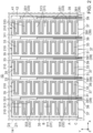
- a touch panel 10 according to an embodiment of the present invention is provided with a base member 12, an electrode layer 14 and a protective layer 16.
- the electrode layer 14 has a conductive pattern formed on a surface of the base member 12.
- the protective layer 16 is provided on the surface of the base member 12 so as to cover the electrode layer 14.
- the base member 12 is a board-like or film-like member.
- the base member 12 is made of a light-transmissive material such as glass or resin.
- the conductive pattern included in the electrode layer 14 may be printed and formed on the surface of the base member 12 by using electrically conductive ink. Alternatively, the conductive pattern included in the electrode layer 14 may be formed by etching a conductive film which is formed on the surface of the base member 12 by any method such as vacuum deposition.
- the protective layer 16 may be formed by spin coating or printing by using ink-like resin. Alternatively, the protective layer 16 may be formed by sticking a cover member made of glass or resin with adhesive.
- the electrode layer 14 has a detection portion 21 and a peripheral portion 23.
- the peripheral portion 23 surrounds the detection portion 21.
- a plurality of first electrodes 31, a plurality of second electrodes (sensor electrodes) 33 and a plurality of dummy electrodes 35 are arranged.
- first lead-out wires 37 are connected, respectively.
- the first lead-out wires 37 are arranged in the peripheral portion 23.
- second lead-out wires (lead-out wires) 39 are connected, respectively.
- the second lead-out wires 39 are arranged from the detection portion 21 to the peripheral portion 23.
- an outer peripheral ground wire 41 is further arranged.
- the outer peripheral ground wire 41 is provided around the detection portion 21.
- each of the first electrodes 31 and the second electrodes 33 is formed in a comb shape.
- each of the first electrodes 31 has a first main portion 311 and a plurality of first facing portions 313.
- the first main portion 311 extends along a first direction.
- the first facing portions 313 extend from the first main portion 311 along a second direction perpendicular to the first direction.
- each of the second electrodes 33 has a second main portion 331 and at least one second facing portion 333.
- the second main portion 331 extends along the first direction.
- the second facing portions 333 extend from the second main portion 331 along the second direction.
- the first direction is a Y-direction
- the second direction is an X-direction.
- the first facing portions 313 extend from the first main portion 311 in a positive X-direction
- the second facing portions 333 extend from the second main portion 331 in a negative x-direction.
- each of the first lead-out wires 37 is laid from the first electrode 31 corresponding thereto in a negative Y-direction.
- each of the second lead-out wires 39 extends from the second electrode 33 corresponding thereto in the negative Y-direction directly or after extending in the positive X-direction.
- the first lead-out wires 37 and the second lead-out wires 39 are electrically separated from one another.
- the first lead-out wires 37 and the second lead-out wires 39 have a common pattern shape.
- the first lead-out wire 37 has a structure similar to that of the second lead-out wire 39 described later with reference to Fig. 3 . However, this may not apply to the peripheral portion 23.
- each of the first lead-out wires 37 and the second lead-out wires 39 is not necessary to have the pattern shape but may be formed as a simple linear wiring line, for example.
- some of the second lead-out wires 39 have elongation portions 391 arranged in the detection portion 21 and extending along the first direction.
- three of four second lead-out wires 39 corresponding to each of the detection rows 210 have the elongation portions 391. These three elongation portions 391 are arranged at predetermined intervals in the second direction.
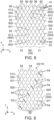
- each of the first electrodes 31 and the second electrodes 33 has a plurality of electrode main portions 50.
- each of the second lead-out wires 39 has a wire main portion 60.
- the sensor electrode 33 has the plurality of the electrode main portions 50
- the lead-out wires 39 have a plurality of the wire main portions 60.
- the electrode main portions 50 and the wire main portions 60 have a common pattern shape.
- the electrode main portions 50 and the wire main portions 60 are arranged at regular intervals in the second direction.
- the unit pattern 600 has the same shape and the same size as those of the unit pattern 500.
- the unit patterns 600 consists of a first portion 611 and a second portion 613.
- the first portion 611 extends in the first diagonal direction
- the second portion 613 extends from one end of the first portion 611 in the second diagonal direction.
- the first portion 611 may extend in the second diagonal direction
- the second portion 613 may extend in the first diagonal direction.
- each of the connection portions 52 extends in the first diagonal direction or the second diagonal direction.
- Each of the connection portions 52 connects two of the first portions 511 which are next to each other in the first diagonal direction to each other or two of the second portions 513 which are adjacent to each other in the second diagonal direction to each other.
- each of the connection portions 52 is as an extension line of the first portions 511 to be connected to each other or the second portions 513 to be connected to each other.
- connection portions 52 closest to each other in the second direction are not located in the same position in the first direction.
- the connection portions 52 closest to each other in the second direction are located in different positions in the first direction. This is because the connection portions 52 becomes more likely to be visually conspicuous when the connection portions 52 closes to each other in the second direction are located in the same position in the first direction.
- the connection portions 52 closest to each other in both of the first direction and the second direction are different in position from each other in the first direction by two times of the unit pattern 500.
- a conductive pattern corresponding to each of the first electrodes 31 of the present embodiment and the second electrodes 33 of the present embodiment forms incomplete reticulation. Accordingly, in an area where the conductive pattern corresponding to each of the first electrodes 31 and the second electrodes 33 is formed, an occupying ratio of the conductive pattern is smaller in comparison with a case of a complete reticulated conductive pattern. In other words, the occupying ratio of the conductive pattern in the area where each of the first electrodes 31 and the second electrodes 33 is close to an occupying ratio of a conductive pattern in an area where the second lead-out wires 39 are formed.
- the outer peripheral ground wire 41 is formed as what is called a solid-pattern wire.
- a space is provided between the outer peripheral ground wire 41 and the first electrode 31, and the outer peripheral ground wire 41 and the first electrode 31 are electrically separated from each other.
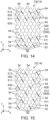
- each of the first electrodes 31 and the second electrodes 33 is provided with the plurality of the electrode main portions 50.
- Each of the electrode main portions 50 is formed by repeatedly arranging the unit patterns 500 in the first direction, wherein each of the unit patterns 500 has the same shape as that of the unit dummy pattern 700 of the second lead-out wire 39.
- the electrode main portions 50 next to each other in the second direction are connected by at least one of the connection portions 52.
- three of the unit patterns 500 which are continuous are connected, by two or less of the connection portions 52, or not connected to one of the electrode main portions 50 which is next thereto in the second direction.
- This structure can further suppress the first electrodes 31 and the second electrodes 33 from being conspicuous in comparison with the second lead-out wires 39. As a result, the viewability of the touch panel 10 is improved.
- connection portions 52 are arranged so that only one of them is provided between the electrode main portions 50 adjacent to each other.
- the connection portions 52 closest to each other in the second direction are different in position from each other in the first direction by a distance corresponding to one of the unit patterns 500.
- connection portions 52 are arranged so that two of them are provided every between the electrode main portions 50 adjacent to each other. Every four of the connection portions 52 forms a group.
- three groups are shown. The three groups are different in position from one another in the second direction.
- Two of the connection portions 52 arranged in the first direction are different in position from each other in the first direction by a distance corresponding to four of the unit patterns 500.
- the connection portions 52 closest to each other in the first direction and the second direction are different in position from each other in the first direction by a distance corresponding to one of the unit patterns 500.
- This arrangement of the connection portions 52 can further reduce an electrical resistance in the second direction in comparison with that of the connection portions 52 of Fig. 9 .
- this arrangement has redundancy for connection between the electrode main portions 50 adjacent to each other, and therefore it has high reliability.
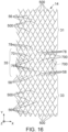
- each of the first intersection portions 80 has two first separation wire portions 801 which are separated from each other in the first diagonal direction. Moreover, the first intersection portion 80 has a first intervention portion 803 extending in the second diagonal direction. The first intervention portion 803 intervenes between the first separation wire portions 801 in the first diagonal direction.
- the second intersection portion 82 has two second separation wire portions 821 which are separated from each other in the second diagonal direction. Moreover, the second intersection portion 82 has a second intervention portion 823 extending in the first diagonal direction. The second intervention portion 823 intervenes between the second separation wire portions 821 in the second diagonal direction.
- the first separation wire portions 801 also serve as the second intervention portions 823
- the first intervention portion 803 also serves as the second separation wire portion 821.
- the first electrode 31 and the second electrode 33 may have, respectively, a first facing portion 313 and a second facing portion 333 which have shapes different from rectangular shapes.
- the second facing portion 333 of the second electrode 33 is formed to have a triangle shape.
- the first facing portion 313 of the first electrode 31 has a shape corresponding to the shape of the second facing portion 333.
- a space exists between the first facing portion 313 and the second facing portion 333. In this space, a dummy electrode 35 may be formed.
Landscapes
- Engineering & Computer Science (AREA)
- General Engineering & Computer Science (AREA)
- Theoretical Computer Science (AREA)
- Human Computer Interaction (AREA)
- Physics & Mathematics (AREA)
- General Physics & Mathematics (AREA)
- Computer Networks & Wireless Communication (AREA)
- Quality & Reliability (AREA)
- Position Input By Displaying (AREA)
- Push-Button Switches (AREA)
Applications Claiming Priority (2)
| Application Number | Priority Date | Filing Date | Title |
|---|---|---|---|
| JP2019209254A JP7425584B2 (ja) | 2019-11-20 | 2019-11-20 | タッチパネル |
| PCT/JP2020/038456 WO2021100354A1 (ja) | 2019-11-20 | 2020-10-12 | タッチパネル |
Publications (3)
| Publication Number | Publication Date |
|---|---|
| EP4030270A1 EP4030270A1 (en) | 2022-07-20 |
| EP4030270A4 EP4030270A4 (en) | 2022-10-12 |
| EP4030270B1 true EP4030270B1 (en) | 2024-07-03 |
Family
ID=75966322
Family Applications (1)
| Application Number | Title | Priority Date | Filing Date |
|---|---|---|---|
| EP20891199.0A Active EP4030270B1 (en) | 2019-11-20 | 2020-10-12 | Touch panel |
Country Status (7)
| Country | Link |
|---|---|
| US (1) | US12014017B2 (enExample) |
| EP (1) | EP4030270B1 (enExample) |
| JP (1) | JP7425584B2 (enExample) |
| KR (1) | KR102613419B1 (enExample) |
| CN (1) | CN114585993B (enExample) |
| TW (1) | TWI774084B (enExample) |
| WO (1) | WO2021100354A1 (enExample) |
Families Citing this family (2)
| Publication number | Priority date | Publication date | Assignee | Title |
|---|---|---|---|---|
| KR20230022009A (ko) * | 2021-08-06 | 2023-02-14 | 동우 화인켐 주식회사 | 터치 센서 |
| WO2024195671A1 (ja) * | 2023-03-23 | 2024-09-26 | 日本精機株式会社 | タッチ入力装置 |
Family Cites Families (20)
| Publication number | Priority date | Publication date | Assignee | Title |
|---|---|---|---|---|
| JP5174745B2 (ja) * | 2009-06-09 | 2013-04-03 | グンゼ株式会社 | タッチスイッチ |
| JP6032532B2 (ja) * | 2012-07-10 | 2016-11-30 | 大日本印刷株式会社 | タッチパネル一体型表示装置用前面保護板、及び表示装置 |
| JP2014089585A (ja) * | 2012-10-30 | 2014-05-15 | Futaba Corp | タッチスイッチ装置 |
| JP6219226B2 (ja) * | 2013-05-16 | 2017-10-25 | 三菱製紙株式会社 | 導電性パターン及び単層静電容量方式タッチパネルの電極パターン |
| JP6170420B2 (ja) * | 2013-12-02 | 2017-07-26 | 富士フイルム株式会社 | 導電シート及びタッチパネル |
| KR102177716B1 (ko) * | 2013-12-30 | 2020-11-11 | 엘지디스플레이 주식회사 | 터치 센서 일체형 표시장치 |
| JP2015232818A (ja) | 2014-06-10 | 2015-12-24 | 株式会社ジャパンディスプレイ | センサ付き表示装置 |
| CN104331205B (zh) * | 2014-11-25 | 2018-10-30 | 上海天马微电子有限公司 | 触控显示装置和电子设备 |
| JP6406575B2 (ja) * | 2014-11-26 | 2018-10-17 | 大日本印刷株式会社 | タッチパネルセンサ、タッチパネル装置および表示装置 |
| JP2016126730A (ja) | 2015-01-08 | 2016-07-11 | 凸版印刷株式会社 | タッチセンサ用電極、タッチパネル、および、表示装置 |
| CN106155396B (zh) * | 2015-04-20 | 2023-05-30 | 苏州诺菲纳米科技有限公司 | 触控传感器 |
| JP2017004289A (ja) | 2015-06-11 | 2017-01-05 | 凸版印刷株式会社 | タッチセンサ用電極およびタッチパネル |
| JP5957132B1 (ja) | 2015-09-30 | 2016-07-27 | 日本航空電子工業株式会社 | タッチパネル |
| CN206339953U (zh) | 2015-10-30 | 2017-07-18 | 株式会社日本显示器 | 传感器以及具备传感器的显示装置 |
| JP6621054B2 (ja) * | 2016-06-27 | 2019-12-18 | ブラザー工業株式会社 | テープ印字装置及びトークデータ処理プログラム |
| EP3564800A1 (en) | 2016-12-28 | 2019-11-06 | Fujikura Ltd. | Wiring body, wiring board and touch sensor |
| JP6511127B2 (ja) | 2017-01-05 | 2019-05-15 | 東友ファインケム株式会社Dongwoo Fine−Chem Co., Ltd. | タッチセンシング電極構造物及びそれを含むタッチセンサー |
| WO2019009315A1 (ja) * | 2017-07-05 | 2019-01-10 | 積水ポリマテック株式会社 | 静電容量式タッチパネル |
| JP6932613B2 (ja) | 2017-10-30 | 2021-09-08 | 株式会社Vtsタッチセンサー | タッチパネル及びそれを備えた表示装置 |
| JP7025015B2 (ja) | 2018-06-05 | 2022-02-24 | ソフタード工業株式会社 | 分離装置及び触媒充填装置 |
-
2019
- 2019-11-20 JP JP2019209254A patent/JP7425584B2/ja active Active
-
2020
- 2020-10-12 EP EP20891199.0A patent/EP4030270B1/en active Active
- 2020-10-12 KR KR1020227013022A patent/KR102613419B1/ko active Active
- 2020-10-12 WO PCT/JP2020/038456 patent/WO2021100354A1/ja not_active Ceased
- 2020-10-12 CN CN202080073342.XA patent/CN114585993B/zh active Active
- 2020-10-12 US US17/766,695 patent/US12014017B2/en active Active
- 2020-10-14 TW TW109135485A patent/TWI774084B/zh active
Also Published As
| Publication number | Publication date |
|---|---|
| CN114585993B (zh) | 2024-05-24 |
| KR20220065836A (ko) | 2022-05-20 |
| US20240028174A1 (en) | 2024-01-25 |
| TWI774084B (zh) | 2022-08-11 |
| WO2021100354A1 (ja) | 2021-05-27 |
| TW202121141A (zh) | 2021-06-01 |
| EP4030270A4 (en) | 2022-10-12 |
| EP4030270A1 (en) | 2022-07-20 |
| KR102613419B1 (ko) | 2023-12-12 |
| US12014017B2 (en) | 2024-06-18 |
| CN114585993A (zh) | 2022-06-03 |
| JP2021082037A (ja) | 2021-05-27 |
| JP7425584B2 (ja) | 2024-01-31 |
Similar Documents
| Publication | Publication Date | Title |
|---|---|---|
| EP2717137B1 (en) | Touch screen panel | |
| US8780071B2 (en) | Capacitive touch panel with multiple zones | |
| EP3680759B1 (en) | Touch substrate and preparation method therefor, and display panel | |
| KR101471753B1 (ko) | 터치 감응전극 구조 | |
| KR102122957B1 (ko) | 터치패널 | |
| US9594454B2 (en) | Touch-panel substrate and electronic device | |
| US9104276B2 (en) | Touch screen panel and manufacturing method thereof | |
| JP2010097536A (ja) | タッチパネル | |
| JPH10505941A (ja) | タッチ検知装置及びその製造方法 | |
| EP4030270B1 (en) | Touch panel | |
| JP2012248181A (ja) | タッチパネルの電極構造、その方法およびタッチパネル | |
| TWI690832B (zh) | 觸控面板 | |
| JP2010182027A (ja) | タッチパネル及びタッチパネルの製造方法 | |
| KR20150079433A (ko) | 터치 스크린 패널 | |
| TWI787293B (zh) | 觸控面板及顯示裝置 | |
| CN112162661B (zh) | 触控显示面板 | |
| CN111045553B (zh) | 触控显示面板和触控显示装置 | |
| CN115033132B (zh) | 触控面板及显示装置 | |
| CN111176484A (zh) | 触控模组及显示面板 | |
| CN102707834B (zh) | 触控面板及其触碰感应层的制造方法 | |
| US20230205378A1 (en) | Conductive sheet, touch sensor, and method for manufacturing touch sensor | |
| JP2013156725A (ja) | タッチパネルおよび表示装置 | |
| CN112860110A (zh) | 触控显示面板 | |
| WO2018149123A1 (zh) | 触控感应结构及制备方法和触控屏 | |
| CN110658957A (zh) | 触控面板 |
Legal Events
| Date | Code | Title | Description |
|---|---|---|---|
| STAA | Information on the status of an ep patent application or granted ep patent |
Free format text: STATUS: THE INTERNATIONAL PUBLICATION HAS BEEN MADE |
|
| PUAI | Public reference made under article 153(3) epc to a published international application that has entered the european phase |
Free format text: ORIGINAL CODE: 0009012 |
|
| STAA | Information on the status of an ep patent application or granted ep patent |
Free format text: STATUS: REQUEST FOR EXAMINATION WAS MADE |
|
| 17P | Request for examination filed |
Effective date: 20220411 |
|
| AK | Designated contracting states |
Kind code of ref document: A1 Designated state(s): AL AT BE BG CH CY CZ DE DK EE ES FI FR GB GR HR HU IE IS IT LI LT LU LV MC MK MT NL NO PL PT RO RS SE SI SK SM TR |
|
| A4 | Supplementary search report drawn up and despatched |
Effective date: 20220908 |
|
| RIC1 | Information provided on ipc code assigned before grant |
Ipc: G06F 3/044 20060101ALI20220902BHEP Ipc: G06F 3/041 20060101AFI20220902BHEP |
|
| DAV | Request for validation of the european patent (deleted) | ||
| DAX | Request for extension of the european patent (deleted) | ||
| STAA | Information on the status of an ep patent application or granted ep patent |
Free format text: STATUS: EXAMINATION IS IN PROGRESS |
|
| 17Q | First examination report despatched |
Effective date: 20230405 |
|
| GRAP | Despatch of communication of intention to grant a patent |
Free format text: ORIGINAL CODE: EPIDOSNIGR1 |
|
| STAA | Information on the status of an ep patent application or granted ep patent |
Free format text: STATUS: GRANT OF PATENT IS INTENDED |
|
| INTG | Intention to grant announced |
Effective date: 20240212 |
|
| GRAS | Grant fee paid |
Free format text: ORIGINAL CODE: EPIDOSNIGR3 |
|
| GRAA | (expected) grant |
Free format text: ORIGINAL CODE: 0009210 |
|
| STAA | Information on the status of an ep patent application or granted ep patent |
Free format text: STATUS: THE PATENT HAS BEEN GRANTED |
|
| AK | Designated contracting states |
Kind code of ref document: B1 Designated state(s): AL AT BE BG CH CY CZ DE DK EE ES FI FR GB GR HR HU IE IS IT LI LT LU LV MC MK MT NL NO PL PT RO RS SE SI SK SM TR |
|
| RAP3 | Party data changed (applicant data changed or rights of an application transferred) |
Owner name: JAPAN AVIATION ELECTRONICS INDUSTRY, LIMITED |
|
| REG | Reference to a national code |
Ref country code: CH Ref legal event code: EP |
|
| REG | Reference to a national code |
Ref country code: DE Ref legal event code: R096 Ref document number: 602020033547 Country of ref document: DE |
|
| REG | Reference to a national code |
Ref country code: LT Ref legal event code: MG9D |
|
| REG | Reference to a national code |
Ref country code: NL Ref legal event code: MP Effective date: 20240703 |
|
| PG25 | Lapsed in a contracting state [announced via postgrant information from national office to epo] |
Ref country code: PT Free format text: LAPSE BECAUSE OF FAILURE TO SUBMIT A TRANSLATION OF THE DESCRIPTION OR TO PAY THE FEE WITHIN THE PRESCRIBED TIME-LIMIT Effective date: 20241104 |
|
| REG | Reference to a national code |
Ref country code: AT Ref legal event code: MK05 Ref document number: 1700515 Country of ref document: AT Kind code of ref document: T Effective date: 20240703 |
|
| PG25 | Lapsed in a contracting state [announced via postgrant information from national office to epo] |
Ref country code: NL Free format text: LAPSE BECAUSE OF FAILURE TO SUBMIT A TRANSLATION OF THE DESCRIPTION OR TO PAY THE FEE WITHIN THE PRESCRIBED TIME-LIMIT Effective date: 20240703 |
|
| PG25 | Lapsed in a contracting state [announced via postgrant information from national office to epo] |
Ref country code: PT Free format text: LAPSE BECAUSE OF FAILURE TO SUBMIT A TRANSLATION OF THE DESCRIPTION OR TO PAY THE FEE WITHIN THE PRESCRIBED TIME-LIMIT Effective date: 20241104 Ref country code: NL Free format text: LAPSE BECAUSE OF FAILURE TO SUBMIT A TRANSLATION OF THE DESCRIPTION OR TO PAY THE FEE WITHIN THE PRESCRIBED TIME-LIMIT Effective date: 20240703 |
|
| PGFP | Annual fee paid to national office [announced via postgrant information from national office to epo] |
Ref country code: DE Payment date: 20241023 Year of fee payment: 5 |
|
| PG25 | Lapsed in a contracting state [announced via postgrant information from national office to epo] |
Ref country code: NO Free format text: LAPSE BECAUSE OF FAILURE TO SUBMIT A TRANSLATION OF THE DESCRIPTION OR TO PAY THE FEE WITHIN THE PRESCRIBED TIME-LIMIT Effective date: 20241003 |
|
| PG25 | Lapsed in a contracting state [announced via postgrant information from national office to epo] |
Ref country code: GR Free format text: LAPSE BECAUSE OF FAILURE TO SUBMIT A TRANSLATION OF THE DESCRIPTION OR TO PAY THE FEE WITHIN THE PRESCRIBED TIME-LIMIT Effective date: 20241004 Ref country code: FI Free format text: LAPSE BECAUSE OF FAILURE TO SUBMIT A TRANSLATION OF THE DESCRIPTION OR TO PAY THE FEE WITHIN THE PRESCRIBED TIME-LIMIT Effective date: 20240703 Ref country code: PL Free format text: LAPSE BECAUSE OF FAILURE TO SUBMIT A TRANSLATION OF THE DESCRIPTION OR TO PAY THE FEE WITHIN THE PRESCRIBED TIME-LIMIT Effective date: 20240703 |
|
| PG25 | Lapsed in a contracting state [announced via postgrant information from national office to epo] |
Ref country code: BG Free format text: LAPSE BECAUSE OF FAILURE TO SUBMIT A TRANSLATION OF THE DESCRIPTION OR TO PAY THE FEE WITHIN THE PRESCRIBED TIME-LIMIT Effective date: 20240703 |
|
| PG25 | Lapsed in a contracting state [announced via postgrant information from national office to epo] |
Ref country code: LV Free format text: LAPSE BECAUSE OF FAILURE TO SUBMIT A TRANSLATION OF THE DESCRIPTION OR TO PAY THE FEE WITHIN THE PRESCRIBED TIME-LIMIT Effective date: 20240703 |
|
| PG25 | Lapsed in a contracting state [announced via postgrant information from national office to epo] |
Ref country code: IS Free format text: LAPSE BECAUSE OF FAILURE TO SUBMIT A TRANSLATION OF THE DESCRIPTION OR TO PAY THE FEE WITHIN THE PRESCRIBED TIME-LIMIT Effective date: 20241103 Ref country code: AT Free format text: LAPSE BECAUSE OF FAILURE TO SUBMIT A TRANSLATION OF THE DESCRIPTION OR TO PAY THE FEE WITHIN THE PRESCRIBED TIME-LIMIT Effective date: 20240703 |
|
| PG25 | Lapsed in a contracting state [announced via postgrant information from national office to epo] |
Ref country code: CZ Free format text: LAPSE BECAUSE OF FAILURE TO SUBMIT A TRANSLATION OF THE DESCRIPTION OR TO PAY THE FEE WITHIN THE PRESCRIBED TIME-LIMIT Effective date: 20240703 Ref country code: HR Free format text: LAPSE BECAUSE OF FAILURE TO SUBMIT A TRANSLATION OF THE DESCRIPTION OR TO PAY THE FEE WITHIN THE PRESCRIBED TIME-LIMIT Effective date: 20240703 |
|
| PG25 | Lapsed in a contracting state [announced via postgrant information from national office to epo] |
Ref country code: RS Free format text: LAPSE BECAUSE OF FAILURE TO SUBMIT A TRANSLATION OF THE DESCRIPTION OR TO PAY THE FEE WITHIN THE PRESCRIBED TIME-LIMIT Effective date: 20241003 Ref country code: ES Free format text: LAPSE BECAUSE OF FAILURE TO SUBMIT A TRANSLATION OF THE DESCRIPTION OR TO PAY THE FEE WITHIN THE PRESCRIBED TIME-LIMIT Effective date: 20240703 |
|
| PG25 | Lapsed in a contracting state [announced via postgrant information from national office to epo] |
Ref country code: RS Free format text: LAPSE BECAUSE OF FAILURE TO SUBMIT A TRANSLATION OF THE DESCRIPTION OR TO PAY THE FEE WITHIN THE PRESCRIBED TIME-LIMIT Effective date: 20241003 Ref country code: PL Free format text: LAPSE BECAUSE OF FAILURE TO SUBMIT A TRANSLATION OF THE DESCRIPTION OR TO PAY THE FEE WITHIN THE PRESCRIBED TIME-LIMIT Effective date: 20240703 Ref country code: NO Free format text: LAPSE BECAUSE OF FAILURE TO SUBMIT A TRANSLATION OF THE DESCRIPTION OR TO PAY THE FEE WITHIN THE PRESCRIBED TIME-LIMIT Effective date: 20241003 Ref country code: LV Free format text: LAPSE BECAUSE OF FAILURE TO SUBMIT A TRANSLATION OF THE DESCRIPTION OR TO PAY THE FEE WITHIN THE PRESCRIBED TIME-LIMIT Effective date: 20240703 Ref country code: IS Free format text: LAPSE BECAUSE OF FAILURE TO SUBMIT A TRANSLATION OF THE DESCRIPTION OR TO PAY THE FEE WITHIN THE PRESCRIBED TIME-LIMIT Effective date: 20241103 Ref country code: HR Free format text: LAPSE BECAUSE OF FAILURE TO SUBMIT A TRANSLATION OF THE DESCRIPTION OR TO PAY THE FEE WITHIN THE PRESCRIBED TIME-LIMIT Effective date: 20240703 Ref country code: GR Free format text: LAPSE BECAUSE OF FAILURE TO SUBMIT A TRANSLATION OF THE DESCRIPTION OR TO PAY THE FEE WITHIN THE PRESCRIBED TIME-LIMIT Effective date: 20241004 Ref country code: FI Free format text: LAPSE BECAUSE OF FAILURE TO SUBMIT A TRANSLATION OF THE DESCRIPTION OR TO PAY THE FEE WITHIN THE PRESCRIBED TIME-LIMIT Effective date: 20240703 Ref country code: ES Free format text: LAPSE BECAUSE OF FAILURE TO SUBMIT A TRANSLATION OF THE DESCRIPTION OR TO PAY THE FEE WITHIN THE PRESCRIBED TIME-LIMIT Effective date: 20240703 Ref country code: CZ Free format text: LAPSE BECAUSE OF FAILURE TO SUBMIT A TRANSLATION OF THE DESCRIPTION OR TO PAY THE FEE WITHIN THE PRESCRIBED TIME-LIMIT Effective date: 20240703 Ref country code: BG Free format text: LAPSE BECAUSE OF FAILURE TO SUBMIT A TRANSLATION OF THE DESCRIPTION OR TO PAY THE FEE WITHIN THE PRESCRIBED TIME-LIMIT Effective date: 20240703 Ref country code: AT Free format text: LAPSE BECAUSE OF FAILURE TO SUBMIT A TRANSLATION OF THE DESCRIPTION OR TO PAY THE FEE WITHIN THE PRESCRIBED TIME-LIMIT Effective date: 20240703 |
|
| REG | Reference to a national code |
Ref country code: DE Ref legal event code: R097 Ref document number: 602020033547 Country of ref document: DE |
|
| PG25 | Lapsed in a contracting state [announced via postgrant information from national office to epo] |
Ref country code: RO Free format text: LAPSE BECAUSE OF FAILURE TO SUBMIT A TRANSLATION OF THE DESCRIPTION OR TO PAY THE FEE WITHIN THE PRESCRIBED TIME-LIMIT Effective date: 20240703 Ref country code: DK Free format text: LAPSE BECAUSE OF FAILURE TO SUBMIT A TRANSLATION OF THE DESCRIPTION OR TO PAY THE FEE WITHIN THE PRESCRIBED TIME-LIMIT Effective date: 20240703 Ref country code: SM Free format text: LAPSE BECAUSE OF FAILURE TO SUBMIT A TRANSLATION OF THE DESCRIPTION OR TO PAY THE FEE WITHIN THE PRESCRIBED TIME-LIMIT Effective date: 20240703 |
|
| PG25 | Lapsed in a contracting state [announced via postgrant information from national office to epo] |
Ref country code: EE Free format text: LAPSE BECAUSE OF FAILURE TO SUBMIT A TRANSLATION OF THE DESCRIPTION OR TO PAY THE FEE WITHIN THE PRESCRIBED TIME-LIMIT Effective date: 20240703 |
|
| PG25 | Lapsed in a contracting state [announced via postgrant information from national office to epo] |
Ref country code: SK Free format text: LAPSE BECAUSE OF FAILURE TO SUBMIT A TRANSLATION OF THE DESCRIPTION OR TO PAY THE FEE WITHIN THE PRESCRIBED TIME-LIMIT Effective date: 20240703 |
|
| PLBE | No opposition filed within time limit |
Free format text: ORIGINAL CODE: 0009261 |
|
| STAA | Information on the status of an ep patent application or granted ep patent |
Free format text: STATUS: NO OPPOSITION FILED WITHIN TIME LIMIT |
|
| REG | Reference to a national code |
Ref country code: CH Ref legal event code: PL |
|
| 26N | No opposition filed |
Effective date: 20250404 |
|
| PG25 | Lapsed in a contracting state [announced via postgrant information from national office to epo] |
Ref country code: MC Free format text: LAPSE BECAUSE OF FAILURE TO SUBMIT A TRANSLATION OF THE DESCRIPTION OR TO PAY THE FEE WITHIN THE PRESCRIBED TIME-LIMIT Effective date: 20240703 |
|
| PG25 | Lapsed in a contracting state [announced via postgrant information from national office to epo] |
Ref country code: LU Free format text: LAPSE BECAUSE OF NON-PAYMENT OF DUE FEES Effective date: 20241012 Ref country code: BE Free format text: LAPSE BECAUSE OF NON-PAYMENT OF DUE FEES Effective date: 20241031 |
|
| PG25 | Lapsed in a contracting state [announced via postgrant information from national office to epo] |
Ref country code: CH Free format text: LAPSE BECAUSE OF NON-PAYMENT OF DUE FEES Effective date: 20241031 |
|
| REG | Reference to a national code |
Ref country code: BE Ref legal event code: MM Effective date: 20241031 |
|
| PG25 | Lapsed in a contracting state [announced via postgrant information from national office to epo] |
Ref country code: SE Free format text: LAPSE BECAUSE OF FAILURE TO SUBMIT A TRANSLATION OF THE DESCRIPTION OR TO PAY THE FEE WITHIN THE PRESCRIBED TIME-LIMIT Effective date: 20240703 |
|
| PGFP | Annual fee paid to national office [announced via postgrant information from national office to epo] |
Ref country code: IT Payment date: 20250922 Year of fee payment: 6 |
|
| PGFP | Annual fee paid to national office [announced via postgrant information from national office to epo] |
Ref country code: GB Payment date: 20250828 Year of fee payment: 6 |
|
| PGFP | Annual fee paid to national office [announced via postgrant information from national office to epo] |
Ref country code: FR Payment date: 20250908 Year of fee payment: 6 |
|
| PG25 | Lapsed in a contracting state [announced via postgrant information from national office to epo] |
Ref country code: IE Free format text: LAPSE BECAUSE OF NON-PAYMENT OF DUE FEES Effective date: 20241012 |