EP4028576B1 - Billes de soudure composites metallisees en surface et calibrees pour l'assemblage de cartes electroniques - Google Patents
Billes de soudure composites metallisees en surface et calibrees pour l'assemblage de cartes electroniques Download PDFInfo
- Publication number
- EP4028576B1 EP4028576B1 EP20767856.6A EP20767856A EP4028576B1 EP 4028576 B1 EP4028576 B1 EP 4028576B1 EP 20767856 A EP20767856 A EP 20767856A EP 4028576 B1 EP4028576 B1 EP 4028576B1
- Authority
- EP
- European Patent Office
- Prior art keywords
- support particles
- copper
- diameter
- particles
- support
- Prior art date
- Legal status (The legal status is an assumption and is not a legal conclusion. Google has not performed a legal analysis and makes no representation as to the accuracy of the status listed.)
- Active
Links
Images


Classifications
-
- C—CHEMISTRY; METALLURGY
- C23—COATING METALLIC MATERIAL; COATING MATERIAL WITH METALLIC MATERIAL; CHEMICAL SURFACE TREATMENT; DIFFUSION TREATMENT OF METALLIC MATERIAL; COATING BY VACUUM EVAPORATION, BY SPUTTERING, BY ION IMPLANTATION OR BY CHEMICAL VAPOUR DEPOSITION, IN GENERAL; INHIBITING CORROSION OF METALLIC MATERIAL OR INCRUSTATION IN GENERAL
- C23C—COATING METALLIC MATERIAL; COATING MATERIAL WITH METALLIC MATERIAL; SURFACE TREATMENT OF METALLIC MATERIAL BY DIFFUSION INTO THE SURFACE, BY CHEMICAL CONVERSION OR SUBSTITUTION; COATING BY VACUUM EVAPORATION, BY SPUTTERING, BY ION IMPLANTATION OR BY CHEMICAL VAPOUR DEPOSITION, IN GENERAL
- C23C18/00—Chemical coating by decomposition of either liquid compounds or solutions of the coating forming compounds, without leaving reaction products of surface material in the coating; Contact plating
- C23C18/16—Chemical coating by decomposition of either liquid compounds or solutions of the coating forming compounds, without leaving reaction products of surface material in the coating; Contact plating by reduction or substitution, e.g. electroless plating
- C23C18/1601—Process or apparatus
- C23C18/1633—Process of electroless plating
- C23C18/1646—Characteristics of the product obtained
- C23C18/165—Multilayered product
- C23C18/1651—Two or more layers only obtained by electroless plating
-
- B—PERFORMING OPERATIONS; TRANSPORTING
- B23—MACHINE TOOLS; METAL-WORKING NOT OTHERWISE PROVIDED FOR
- B23K—SOLDERING OR UNSOLDERING; WELDING; CLADDING OR PLATING BY SOLDERING OR WELDING; CUTTING BY APPLYING HEAT LOCALLY, e.g. FLAME CUTTING; WORKING BY LASER BEAM
- B23K35/00—Rods, electrodes, materials, or media, for use in soldering, welding, or cutting
- B23K35/02—Rods, electrodes, materials, or media, for use in soldering, welding, or cutting characterised by mechanical features, e.g. shape
- B23K35/0222—Rods, electrodes, materials, or media, for use in soldering, welding, or cutting characterised by mechanical features, e.g. shape for use in soldering or brazing
-
- B—PERFORMING OPERATIONS; TRANSPORTING
- B23—MACHINE TOOLS; METAL-WORKING NOT OTHERWISE PROVIDED FOR
- B23K—SOLDERING OR UNSOLDERING; WELDING; CLADDING OR PLATING BY SOLDERING OR WELDING; CUTTING BY APPLYING HEAT LOCALLY, e.g. FLAME CUTTING; WORKING BY LASER BEAM
- B23K35/00—Rods, electrodes, materials, or media, for use in soldering, welding, or cutting
- B23K35/02—Rods, electrodes, materials, or media, for use in soldering, welding, or cutting characterised by mechanical features, e.g. shape
- B23K35/0222—Rods, electrodes, materials, or media, for use in soldering, welding, or cutting characterised by mechanical features, e.g. shape for use in soldering or brazing
- B23K35/0244—Powders, particles or spheres; Preforms made therefrom
-
- B—PERFORMING OPERATIONS; TRANSPORTING
- B23—MACHINE TOOLS; METAL-WORKING NOT OTHERWISE PROVIDED FOR
- B23K—SOLDERING OR UNSOLDERING; WELDING; CLADDING OR PLATING BY SOLDERING OR WELDING; CUTTING BY APPLYING HEAT LOCALLY, e.g. FLAME CUTTING; WORKING BY LASER BEAM
- B23K35/00—Rods, electrodes, materials, or media, for use in soldering, welding, or cutting
- B23K35/22—Rods, electrodes, materials, or media, for use in soldering, welding, or cutting characterised by the composition or nature of the material
- B23K35/24—Selection of soldering or welding materials proper
-
- B—PERFORMING OPERATIONS; TRANSPORTING
- B23—MACHINE TOOLS; METAL-WORKING NOT OTHERWISE PROVIDED FOR
- B23K—SOLDERING OR UNSOLDERING; WELDING; CLADDING OR PLATING BY SOLDERING OR WELDING; CUTTING BY APPLYING HEAT LOCALLY, e.g. FLAME CUTTING; WORKING BY LASER BEAM
- B23K35/00—Rods, electrodes, materials, or media, for use in soldering, welding, or cutting
- B23K35/22—Rods, electrodes, materials, or media, for use in soldering, welding, or cutting characterised by the composition or nature of the material
- B23K35/24—Selection of soldering or welding materials proper
- B23K35/30—Selection of soldering or welding materials proper with the principal constituent melting at less than 1550°C
- B23K35/3006—Ag as the principal constituent
-
- B—PERFORMING OPERATIONS; TRANSPORTING
- B23—MACHINE TOOLS; METAL-WORKING NOT OTHERWISE PROVIDED FOR
- B23K—SOLDERING OR UNSOLDERING; WELDING; CLADDING OR PLATING BY SOLDERING OR WELDING; CUTTING BY APPLYING HEAT LOCALLY, e.g. FLAME CUTTING; WORKING BY LASER BEAM
- B23K35/00—Rods, electrodes, materials, or media, for use in soldering, welding, or cutting
- B23K35/22—Rods, electrodes, materials, or media, for use in soldering, welding, or cutting characterised by the composition or nature of the material
- B23K35/24—Selection of soldering or welding materials proper
- B23K35/30—Selection of soldering or welding materials proper with the principal constituent melting at less than 1550°C
- B23K35/302—Cu as the principal constituent
-
- B—PERFORMING OPERATIONS; TRANSPORTING
- B23—MACHINE TOOLS; METAL-WORKING NOT OTHERWISE PROVIDED FOR
- B23K—SOLDERING OR UNSOLDERING; WELDING; CLADDING OR PLATING BY SOLDERING OR WELDING; CUTTING BY APPLYING HEAT LOCALLY, e.g. FLAME CUTTING; WORKING BY LASER BEAM
- B23K35/00—Rods, electrodes, materials, or media, for use in soldering, welding, or cutting
- B23K35/22—Rods, electrodes, materials, or media, for use in soldering, welding, or cutting characterised by the composition or nature of the material
- B23K35/24—Selection of soldering or welding materials proper
- B23K35/30—Selection of soldering or welding materials proper with the principal constituent melting at less than 1550°C
- B23K35/3033—Ni as the principal constituent
-
- C—CHEMISTRY; METALLURGY
- C23—COATING METALLIC MATERIAL; COATING MATERIAL WITH METALLIC MATERIAL; CHEMICAL SURFACE TREATMENT; DIFFUSION TREATMENT OF METALLIC MATERIAL; COATING BY VACUUM EVAPORATION, BY SPUTTERING, BY ION IMPLANTATION OR BY CHEMICAL VAPOUR DEPOSITION, IN GENERAL; INHIBITING CORROSION OF METALLIC MATERIAL OR INCRUSTATION IN GENERAL
- C23C—COATING METALLIC MATERIAL; COATING MATERIAL WITH METALLIC MATERIAL; SURFACE TREATMENT OF METALLIC MATERIAL BY DIFFUSION INTO THE SURFACE, BY CHEMICAL CONVERSION OR SUBSTITUTION; COATING BY VACUUM EVAPORATION, BY SPUTTERING, BY ION IMPLANTATION OR BY CHEMICAL VAPOUR DEPOSITION, IN GENERAL
- C23C18/00—Chemical coating by decomposition of either liquid compounds or solutions of the coating forming compounds, without leaving reaction products of surface material in the coating; Contact plating
- C23C18/16—Chemical coating by decomposition of either liquid compounds or solutions of the coating forming compounds, without leaving reaction products of surface material in the coating; Contact plating by reduction or substitution, e.g. electroless plating
- C23C18/1601—Process or apparatus
- C23C18/1633—Process of electroless plating
- C23C18/1635—Composition of the substrate
- C23C18/1639—Substrates other than metallic, e.g. inorganic or organic or non-conductive
- C23C18/1641—Organic substrates, e.g. resin, plastic
-
- C—CHEMISTRY; METALLURGY
- C23—COATING METALLIC MATERIAL; COATING MATERIAL WITH METALLIC MATERIAL; CHEMICAL SURFACE TREATMENT; DIFFUSION TREATMENT OF METALLIC MATERIAL; COATING BY VACUUM EVAPORATION, BY SPUTTERING, BY ION IMPLANTATION OR BY CHEMICAL VAPOUR DEPOSITION, IN GENERAL; INHIBITING CORROSION OF METALLIC MATERIAL OR INCRUSTATION IN GENERAL
- C23C—COATING METALLIC MATERIAL; COATING MATERIAL WITH METALLIC MATERIAL; SURFACE TREATMENT OF METALLIC MATERIAL BY DIFFUSION INTO THE SURFACE, BY CHEMICAL CONVERSION OR SUBSTITUTION; COATING BY VACUUM EVAPORATION, BY SPUTTERING, BY ION IMPLANTATION OR BY CHEMICAL VAPOUR DEPOSITION, IN GENERAL
- C23C18/00—Chemical coating by decomposition of either liquid compounds or solutions of the coating forming compounds, without leaving reaction products of surface material in the coating; Contact plating
- C23C18/16—Chemical coating by decomposition of either liquid compounds or solutions of the coating forming compounds, without leaving reaction products of surface material in the coating; Contact plating by reduction or substitution, e.g. electroless plating
- C23C18/1601—Process or apparatus
- C23C18/1633—Process of electroless plating
- C23C18/1655—Process features
- C23C18/1657—Electroless forming, i.e. substrate removed or destroyed at the end of the process
-
- C—CHEMISTRY; METALLURGY
- C23—COATING METALLIC MATERIAL; COATING MATERIAL WITH METALLIC MATERIAL; CHEMICAL SURFACE TREATMENT; DIFFUSION TREATMENT OF METALLIC MATERIAL; COATING BY VACUUM EVAPORATION, BY SPUTTERING, BY ION IMPLANTATION OR BY CHEMICAL VAPOUR DEPOSITION, IN GENERAL; INHIBITING CORROSION OF METALLIC MATERIAL OR INCRUSTATION IN GENERAL
- C23C—COATING METALLIC MATERIAL; COATING MATERIAL WITH METALLIC MATERIAL; SURFACE TREATMENT OF METALLIC MATERIAL BY DIFFUSION INTO THE SURFACE, BY CHEMICAL CONVERSION OR SUBSTITUTION; COATING BY VACUUM EVAPORATION, BY SPUTTERING, BY ION IMPLANTATION OR BY CHEMICAL VAPOUR DEPOSITION, IN GENERAL
- C23C18/00—Chemical coating by decomposition of either liquid compounds or solutions of the coating forming compounds, without leaving reaction products of surface material in the coating; Contact plating
- C23C18/16—Chemical coating by decomposition of either liquid compounds or solutions of the coating forming compounds, without leaving reaction products of surface material in the coating; Contact plating by reduction or substitution, e.g. electroless plating
- C23C18/1601—Process or apparatus
- C23C18/1633—Process of electroless plating
- C23C18/1689—After-treatment
- C23C18/1692—Heat-treatment
-
- C—CHEMISTRY; METALLURGY
- C23—COATING METALLIC MATERIAL; COATING MATERIAL WITH METALLIC MATERIAL; CHEMICAL SURFACE TREATMENT; DIFFUSION TREATMENT OF METALLIC MATERIAL; COATING BY VACUUM EVAPORATION, BY SPUTTERING, BY ION IMPLANTATION OR BY CHEMICAL VAPOUR DEPOSITION, IN GENERAL; INHIBITING CORROSION OF METALLIC MATERIAL OR INCRUSTATION IN GENERAL
- C23C—COATING METALLIC MATERIAL; COATING MATERIAL WITH METALLIC MATERIAL; SURFACE TREATMENT OF METALLIC MATERIAL BY DIFFUSION INTO THE SURFACE, BY CHEMICAL CONVERSION OR SUBSTITUTION; COATING BY VACUUM EVAPORATION, BY SPUTTERING, BY ION IMPLANTATION OR BY CHEMICAL VAPOUR DEPOSITION, IN GENERAL
- C23C18/00—Chemical coating by decomposition of either liquid compounds or solutions of the coating forming compounds, without leaving reaction products of surface material in the coating; Contact plating
- C23C18/16—Chemical coating by decomposition of either liquid compounds or solutions of the coating forming compounds, without leaving reaction products of surface material in the coating; Contact plating by reduction or substitution, e.g. electroless plating
- C23C18/18—Pretreatment of the material to be coated
- C23C18/20—Pretreatment of the material to be coated of organic surfaces, e.g. resins
- C23C18/2006—Pretreatment of the material to be coated of organic surfaces, e.g. resins by other methods than those of C23C18/22 - C23C18/30
- C23C18/2046—Pretreatment of the material to be coated of organic surfaces, e.g. resins by other methods than those of C23C18/22 - C23C18/30 by chemical pretreatment
- C23C18/2053—Pretreatment of the material to be coated of organic surfaces, e.g. resins by other methods than those of C23C18/22 - C23C18/30 by chemical pretreatment only one step pretreatment
- C23C18/206—Use of metal other than noble metals and tin, e.g. activation, sensitisation with metals
-
- C—CHEMISTRY; METALLURGY
- C23—COATING METALLIC MATERIAL; COATING MATERIAL WITH METALLIC MATERIAL; CHEMICAL SURFACE TREATMENT; DIFFUSION TREATMENT OF METALLIC MATERIAL; COATING BY VACUUM EVAPORATION, BY SPUTTERING, BY ION IMPLANTATION OR BY CHEMICAL VAPOUR DEPOSITION, IN GENERAL; INHIBITING CORROSION OF METALLIC MATERIAL OR INCRUSTATION IN GENERAL
- C23C—COATING METALLIC MATERIAL; COATING MATERIAL WITH METALLIC MATERIAL; SURFACE TREATMENT OF METALLIC MATERIAL BY DIFFUSION INTO THE SURFACE, BY CHEMICAL CONVERSION OR SUBSTITUTION; COATING BY VACUUM EVAPORATION, BY SPUTTERING, BY ION IMPLANTATION OR BY CHEMICAL VAPOUR DEPOSITION, IN GENERAL
- C23C18/00—Chemical coating by decomposition of either liquid compounds or solutions of the coating forming compounds, without leaving reaction products of surface material in the coating; Contact plating
- C23C18/16—Chemical coating by decomposition of either liquid compounds or solutions of the coating forming compounds, without leaving reaction products of surface material in the coating; Contact plating by reduction or substitution, e.g. electroless plating
- C23C18/18—Pretreatment of the material to be coated
- C23C18/20—Pretreatment of the material to be coated of organic surfaces, e.g. resins
- C23C18/28—Sensitising or activating
- C23C18/30—Activating or accelerating or sensitising with palladium or other noble metal
-
- C—CHEMISTRY; METALLURGY
- C23—COATING METALLIC MATERIAL; COATING MATERIAL WITH METALLIC MATERIAL; CHEMICAL SURFACE TREATMENT; DIFFUSION TREATMENT OF METALLIC MATERIAL; COATING BY VACUUM EVAPORATION, BY SPUTTERING, BY ION IMPLANTATION OR BY CHEMICAL VAPOUR DEPOSITION, IN GENERAL; INHIBITING CORROSION OF METALLIC MATERIAL OR INCRUSTATION IN GENERAL
- C23C—COATING METALLIC MATERIAL; COATING MATERIAL WITH METALLIC MATERIAL; SURFACE TREATMENT OF METALLIC MATERIAL BY DIFFUSION INTO THE SURFACE, BY CHEMICAL CONVERSION OR SUBSTITUTION; COATING BY VACUUM EVAPORATION, BY SPUTTERING, BY ION IMPLANTATION OR BY CHEMICAL VAPOUR DEPOSITION, IN GENERAL
- C23C18/00—Chemical coating by decomposition of either liquid compounds or solutions of the coating forming compounds, without leaving reaction products of surface material in the coating; Contact plating
- C23C18/16—Chemical coating by decomposition of either liquid compounds or solutions of the coating forming compounds, without leaving reaction products of surface material in the coating; Contact plating by reduction or substitution, e.g. electroless plating
- C23C18/31—Coating with metals
- C23C18/32—Coating with nickel, cobalt or mixtures thereof with phosphorus or boron
-
- C—CHEMISTRY; METALLURGY
- C23—COATING METALLIC MATERIAL; COATING MATERIAL WITH METALLIC MATERIAL; CHEMICAL SURFACE TREATMENT; DIFFUSION TREATMENT OF METALLIC MATERIAL; COATING BY VACUUM EVAPORATION, BY SPUTTERING, BY ION IMPLANTATION OR BY CHEMICAL VAPOUR DEPOSITION, IN GENERAL; INHIBITING CORROSION OF METALLIC MATERIAL OR INCRUSTATION IN GENERAL
- C23C—COATING METALLIC MATERIAL; COATING MATERIAL WITH METALLIC MATERIAL; SURFACE TREATMENT OF METALLIC MATERIAL BY DIFFUSION INTO THE SURFACE, BY CHEMICAL CONVERSION OR SUBSTITUTION; COATING BY VACUUM EVAPORATION, BY SPUTTERING, BY ION IMPLANTATION OR BY CHEMICAL VAPOUR DEPOSITION, IN GENERAL
- C23C18/00—Chemical coating by decomposition of either liquid compounds or solutions of the coating forming compounds, without leaving reaction products of surface material in the coating; Contact plating
- C23C18/16—Chemical coating by decomposition of either liquid compounds or solutions of the coating forming compounds, without leaving reaction products of surface material in the coating; Contact plating by reduction or substitution, e.g. electroless plating
- C23C18/31—Coating with metals
- C23C18/38—Coating with copper
-
- C—CHEMISTRY; METALLURGY
- C23—COATING METALLIC MATERIAL; COATING MATERIAL WITH METALLIC MATERIAL; CHEMICAL SURFACE TREATMENT; DIFFUSION TREATMENT OF METALLIC MATERIAL; COATING BY VACUUM EVAPORATION, BY SPUTTERING, BY ION IMPLANTATION OR BY CHEMICAL VAPOUR DEPOSITION, IN GENERAL; INHIBITING CORROSION OF METALLIC MATERIAL OR INCRUSTATION IN GENERAL
- C23C—COATING METALLIC MATERIAL; COATING MATERIAL WITH METALLIC MATERIAL; SURFACE TREATMENT OF METALLIC MATERIAL BY DIFFUSION INTO THE SURFACE, BY CHEMICAL CONVERSION OR SUBSTITUTION; COATING BY VACUUM EVAPORATION, BY SPUTTERING, BY ION IMPLANTATION OR BY CHEMICAL VAPOUR DEPOSITION, IN GENERAL
- C23C18/00—Chemical coating by decomposition of either liquid compounds or solutions of the coating forming compounds, without leaving reaction products of surface material in the coating; Contact plating
- C23C18/54—Contact plating, i.e. electroless electrochemical plating
-
- H—ELECTRICITY
- H05—ELECTRIC TECHNIQUES NOT OTHERWISE PROVIDED FOR
- H05K—PRINTED CIRCUITS; CASINGS OR CONSTRUCTIONAL DETAILS OF ELECTRIC APPARATUS; MANUFACTURE OF ASSEMBLAGES OF ELECTRICAL COMPONENTS
- H05K1/00—Printed circuits
- H05K1/02—Details
- H05K1/0271—Arrangements for reducing stress or warp in rigid printed circuit boards, e.g. caused by loads, vibrations or differences in thermal expansion
-
- H—ELECTRICITY
- H05—ELECTRIC TECHNIQUES NOT OTHERWISE PROVIDED FOR
- H05K—PRINTED CIRCUITS; CASINGS OR CONSTRUCTIONAL DETAILS OF ELECTRIC APPARATUS; MANUFACTURE OF ASSEMBLAGES OF ELECTRICAL COMPONENTS
- H05K3/00—Apparatus or processes for manufacturing printed circuits
- H05K3/30—Assembling printed circuits with electric components, e.g. with resistors
- H05K3/32—Assembling printed circuits with electric components, e.g. with resistors electrically connecting electric components or wires to printed circuits
- H05K3/34—Assembling printed circuits with electric components, e.g. with resistors electrically connecting electric components or wires to printed circuits by soldering
- H05K3/341—Surface mounted components
- H05K3/3431—Leadless components
- H05K3/3436—Leadless components having an array of bottom contacts, e.g. pad grid array or ball grid array components
-
- H—ELECTRICITY
- H05—ELECTRIC TECHNIQUES NOT OTHERWISE PROVIDED FOR
- H05K—PRINTED CIRCUITS; CASINGS OR CONSTRUCTIONAL DETAILS OF ELECTRIC APPARATUS; MANUFACTURE OF ASSEMBLAGES OF ELECTRICAL COMPONENTS
- H05K3/00—Apparatus or processes for manufacturing printed circuits
- H05K3/30—Assembling printed circuits with electric components, e.g. with resistors
- H05K3/32—Assembling printed circuits with electric components, e.g. with resistors electrically connecting electric components or wires to printed circuits
- H05K3/34—Assembling printed circuits with electric components, e.g. with resistors electrically connecting electric components or wires to printed circuits by soldering
- H05K3/3465—Application of solder
- H05K3/3473—Plating of solder
-
- C—CHEMISTRY; METALLURGY
- C23—COATING METALLIC MATERIAL; COATING MATERIAL WITH METALLIC MATERIAL; CHEMICAL SURFACE TREATMENT; DIFFUSION TREATMENT OF METALLIC MATERIAL; COATING BY VACUUM EVAPORATION, BY SPUTTERING, BY ION IMPLANTATION OR BY CHEMICAL VAPOUR DEPOSITION, IN GENERAL; INHIBITING CORROSION OF METALLIC MATERIAL OR INCRUSTATION IN GENERAL
- C23C—COATING METALLIC MATERIAL; COATING MATERIAL WITH METALLIC MATERIAL; SURFACE TREATMENT OF METALLIC MATERIAL BY DIFFUSION INTO THE SURFACE, BY CHEMICAL CONVERSION OR SUBSTITUTION; COATING BY VACUUM EVAPORATION, BY SPUTTERING, BY ION IMPLANTATION OR BY CHEMICAL VAPOUR DEPOSITION, IN GENERAL
- C23C18/00—Chemical coating by decomposition of either liquid compounds or solutions of the coating forming compounds, without leaving reaction products of surface material in the coating; Contact plating
- C23C18/16—Chemical coating by decomposition of either liquid compounds or solutions of the coating forming compounds, without leaving reaction products of surface material in the coating; Contact plating by reduction or substitution, e.g. electroless plating
- C23C18/1601—Process or apparatus
- C23C18/1633—Process of electroless plating
- C23C18/1635—Composition of the substrate
-
- H—ELECTRICITY
- H05—ELECTRIC TECHNIQUES NOT OTHERWISE PROVIDED FOR
- H05K—PRINTED CIRCUITS; CASINGS OR CONSTRUCTIONAL DETAILS OF ELECTRIC APPARATUS; MANUFACTURE OF ASSEMBLAGES OF ELECTRICAL COMPONENTS
- H05K2201/00—Indexing scheme relating to printed circuits covered by H05K1/00
- H05K2201/10—Details of components or other objects attached to or integrated in a printed circuit board
- H05K2201/10613—Details of electrical connections of non-printed components, e.g. special leads
- H05K2201/10621—Components characterised by their electrical contacts
- H05K2201/10734—Ball grid array [BGA]; Bump grid array
-
- H—ELECTRICITY
- H05—ELECTRIC TECHNIQUES NOT OTHERWISE PROVIDED FOR
- H05K—PRINTED CIRCUITS; CASINGS OR CONSTRUCTIONAL DETAILS OF ELECTRIC APPARATUS; MANUFACTURE OF ASSEMBLAGES OF ELECTRICAL COMPONENTS
- H05K2203/00—Indexing scheme relating to apparatus or processes for manufacturing printed circuits covered by H05K3/00
- H05K2203/04—Soldering or other types of metallurgic bonding
- H05K2203/0435—Metal coated solder, e.g. for passivation of solder balls
Definitions
- the present invention generally relates to the manufacture of composite solder balls and the use of these balls as an interconnection solution for the assembly of electronic cards.
- Soft balls are one of the technologies used to create systems in a package, generally referred to by the English acronym SiP (for “ System In Package ”). They have solder contacts allowing them to be easily assembled in the case.
- the flexible balls currently used in this field have the disadvantage of being made up of a dense core of polymer material, negatively impacting the manufacturing costs linked to the yields of the manufacturing and calibration processes of the balls. initials, as well as the final density of the ball.
- differential thermal expansion problems may be encountered between the core and the metallic envelope of the particles during subsequent brazing operations.
- the Applicant has developed a process for manufacturing surface-metallized and calibrated composite solder balls, said balls comprising a core consisting of a spherical-shaped support particle of diameter D 0 , made of expanded polystyrene ( PSE) and having an intragranular porosity of at least 50%, and an envelope covering said support particle and formed by a plurality of metallic surface layers, comprising in particular a copper coating of thickness E cu , at least one layer of nickel d thickness E Ni , and a finishing layer of gold with a thickness E Au such that the final particle has a diameter D f .
- PSE expanded polystyrene
- Expanded polystyrene (EPS) beads have the advantage of being able to reduce in size when heated and thus offer the possibility of being calibrated by heat treatment.
- intragranular porosity is meant, within the meaning of the present invention, the internal porosity of a support particle, on the surface and/or inside which different types of pores can be observed: channels, networks, "pockets", non-opening pores and surface roughness. It can be measured for example by Helium pycnometry.
- the first step of the process according to the invention is the step of supplying support particles (step A).
- EPS expanded polystyrene
- step B we begin by carrying out a first particle size sorting of these support particles (step B), consisting of a step of physical and/or mechanical separation of the support particles (10) having a diameter D 0 chosen between 200 ⁇ m and 1000 ⁇ m.
- the particle size sorting step B) of the support particles may consist of mechanical sieving to sort and select the support particles having a diameter D0 chosen between 200 ⁇ m and 1000 ⁇ m.
- support particles whose size corresponds to the target value D 0 +/- 5%.
- the particle size sorting step B) of the support particles may consist of mechanical sieving of the support particles. It can then advantageously be completed by a heat treatment at a temperature between 100°C and 120°C, and preferably between 110°C and 120°C, of the upper portion of the particles thus sorted (i.e. say particles whose size is greater than D 0 +5%, in order to increase the calibration efficiency of the initial population of beads.
- EPS expanded polystyrene
- an activation treatment is carried out (step C) of the previously selected support particles, to obtain activated support particles.
- activation treatment is meant, within the meaning of the present invention, a treatment consisting of activating the surface of the support particles in order to allow good adhesion of the subsequent metallization treatment.
- a first advantageous embodiment of this activation treatment could for example consist of depositing, on the surface of the previously selected support particles, silver seeds by reduction of silver ions in solution, the silver deposition being done by germination-growth.
- the operation can for example be carried out by reduction of an ammoniacal silver nitrate in a glycol-based solution.
- Another advantageous embodiment of this activation treatment may also consist of depositing, on the surface of the previously selected support particles, copper in a thin layer less than or equal to 1 ⁇ m, by physical vapor deposition (PVD).
- PVD physical vapor deposition
- the first metallization step (step D) of the activated support particles is a step of auto-catalytic chemical deposition of one or more layers of copper, this step being repeated until a thickness Ecu of copper layer of between 15 ⁇ m and 35 ⁇ m, to obtain copper-coated support particles. Several successive metallizations may be necessary to obtain the desired copper thickness.
- solder balls we can carry out between metallization stages D and E, either a partial or total dissolution, or a partial or total thermal decomposition of the expanded polystyrene. (PSE) constituting the support particles.
- PSE expanded polystyrene
- the second metallization step (step E) consists of metallizing the copper-coated support particles obtained at the end of step D) (possibly transformed into hollow or quasi-hollow balls) by auto-catalytic chemical deposition of at least one layer of nickel alloyed with phosphorus NiP with a mass percentage of 7 to 10% of phosphorus relative to the total weight of the layer of NiP (or chemical nickel).
- This step E) is carried out until a thickness ENi of chemical nickel layer (111) of between 4 ⁇ m and 7 ⁇ m is obtained, to obtain support particles coated with chemical nickel.
- the third metallization step (step F) consists of metallizing the support particles coated with chemical nickel by immersion in a solution containing gold ions, so as to obtain metallized composite solder balls coated on the surface with a layer of gold finish with a thickness E Au between 0.05 ⁇ m and 0.12 ⁇ m.
- step G is a second step of particle size sorting of the particles thus metallized to sort and select composite solder balls metallized on the surface having a diameter D f with a tolerance of +/- 5%.
- the present invention also relates to solder balls capable of being obtained by the manufacturing process according to the invention.
- solder balls according to the invention can be hollow (or quasi-hollow) balls comprising a core made up of at most 50% by volume of polymer material when it is expanded polystyrene (EPS).
- EPS expanded polystyrene
- Such solder balls are obtained with the process according to the invention when the latter comprises, between steps D) and E), a partial or total dissolution step, a partial or total thermal decomposition step of the expanded polystyrene (EPS). ) constitutive of the starting support particles.
- the present invention also relates to the use of the balls according to the invention, for the assembly of electronic cards.
- the structure of the balls according to the invention makes it possible to make interconnections between components sensitive to mechanical stresses (CBGA, MEMS, etc.). They also have the advantage of, on the one hand, maintaining controlled positioning, and on the other hand, limiting mechanical constraints in the interconnections between substrate and components.
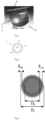
- Fig. 1 is described in the presentation of the known state of the art. It shows in particular flexible balls having solder contacts 1, 2 allowing them to be easily assembled.
- Fig. 2 to Fig. 12 are described in more detail in the examples which follow, which illustrate the invention without limiting its scope.
- Optical microscope observations are carried out using an optical microscope, on the surface ([ Fig. 4] to [Fig. 7 ]) and in cross section ([ Fig. 8] and [Fig. 9 ]).
- Solder balls according to the invention are produced in the same way as in Example 1 with support balls of 660 ⁇ m in diameter and a copper deposit of the order of 15 to 17 ⁇ m thick (cf. Figure 8 and 9A ).
- Solder balls according to the invention are produced in the same way as in examples 1 and 2, in order to obtain balls with a diameter D f of the order of 400 ⁇ m +/-5% (see [ Fig. 12 ]).
- the beads produced according to the present invention from expanded polystyrene have a mass reduction factor of between 1.7 and 9.4 compared to current solutions (dense core of organic or metallic material).
- the thermal stability of the balls is improved with the use of an EPS core (balls according to the invention of the first batch) compared to the balls obtained from a dense core (balls of the second and third batches).
- the beads made from dense polystyrene show a behavioral defect with the appearance of “droplets” of organic matter on the surface of the beads ( Figure 1 ). The phenomenon is not observed on the beads according to the invention made from expanded polystyrene (beads from the first batch).
Landscapes
- Chemical & Material Sciences (AREA)
- Engineering & Computer Science (AREA)
- Mechanical Engineering (AREA)
- Metallurgy (AREA)
- Organic Chemistry (AREA)
- General Chemical & Material Sciences (AREA)
- Chemical Kinetics & Catalysis (AREA)
- Materials Engineering (AREA)
- Microelectronics & Electronic Packaging (AREA)
- Electrochemistry (AREA)
- Manufacturing & Machinery (AREA)
- Inorganic Chemistry (AREA)
- Other Surface Treatments For Metallic Materials (AREA)
- Powder Metallurgy (AREA)
- Electroplating Methods And Accessories (AREA)
- Electric Connection Of Electric Components To Printed Circuits (AREA)
- Chemically Coating (AREA)
- Details Of Resistors (AREA)
Description
- La présente invention concerne de manière générale la fabrication de billes de soudure composites et l'utilisation de ces billes comme solution d'interconnexion pour l'assemblage de cartes électroniques.
- La recherche de technologies pour l'assemblage de cartes électroniques de plus en plus miniaturisées et n'utilisant pas de plomb incitent de plus en plus les acteurs industriels dans ce domaine technologique à chercher des solutions innovantes pour réaliser des interconnexions entre des composants sensibles aux contraintes mécaniques, par exemple des matrices de billes de type CBGA (acronyme anglais pour « Ceramic Ball Grid Array »), ou des microsystèmes électromécaniques (couramment désignés par l'acronyme anglais MEMS pour « Micro Electro Mechanical System »). Le document
JP6500583 - Les billes souples (telles qu'illustrées sur [
Fig. 1 ]) sont une des technologies utilisées pour réaliser des systèmes dans un boitier, généralement désignés par l'acronyme anglais SiP (pour « System In Package »). Elles présentent des contacts à souder permettant facilement leur assemblage dans le boitier. - Toutefois, à l'heure actuelle, les billes souples actuellement utilisées dans ce domaine présentent l'inconvénient d'être constituées d'un coeur dense en matériau polymère impactant négativement les coûts de fabrications liés aux rendements des processus de fabrication et de calibration des billes initiales, ainsi qu'à la densité finale de la bille. D'autre part, des problèmes de dilatations thermiques différentielles peuvent être rencontrés entre le coeur et l'enveloppe métallique des particules lors des opérations de brasages ultérieures.
- Afin de remédier à cet inconvénient, le Demandeur a mis au point un procédé de fabrication de billes de soudure composites métallisées en surface et calibrées, lesdites billes comprenant un coeur constitué par une particule support de forme sphérique de diamètre D0, en polystyrène expansé (PSE) et présentant une porosité intragranulaire d'au moins 50%, et une enveloppe recouvrant ladite particule support et formée par une pluralité de couches superficielles métalliques, comprenant notamment un revêtement de cuivre d'épaisseur Ecu, au moins une couche de nickel d'épaisseur ENi, et une couche de finition d'or d'une épaisseur EAu de telle sorte que la particule finale possède un diamètre Df.
- Selon l'invention, le procédé est caractérisé en ce qu'il comprend les étapes suivantes:
- A) une première étape de fourniture de particules support, suivie par
- B) une première étape de tri granulométrique desdites particules support, consistant en une étape de séparation physique et/ou mécanique des particules support présentant un diamètre D0 avec une tolérance +/-5% tel que D0 = Df-2∗(ENi+ECu+EAu), Do pouvant être choisi entre 200 µm et 1000 µm ;
- C) une étape de traitement d'activation des particules support ainsi sélectionnées, pour obtenir des particules support activées ;
- D) une première étape de métallisation desdites particules support activées par dépôt chimique auto-catalytique d'une ou plusieurs couches de cuivre, cette étape étant répétée jusqu'à obtention d'une épaisseur Ecu de couche de cuivre comprise entre 15 µm et 35 µm, pour obtenir des particules support revêtues de cuivre ;
- E) une deuxième étape de métallisation des particules support revêtues de cuivre par dépôt chimique auto-catalytique d'au moins une couche de nickel allié à du phosphore NiP avec un pourcentage massique de 7 à 10% de phosphore par rapport au poids total de ladite couche de NiP, cette étape étant conduite jusqu'à obtention d'une épaisseur ENi de couche de nickel chimique comprise entre 4 µm et 7 µm, pour obtenir des particules support revêtues de nickel chimique ;
- F) une troisième étape de métallisation des particules support revêtues de nickel chimique (consistant en une étape de dépôt d'or par un procédé de déplacement galvanique réalisé par immersion dans une solution aqueuse contenant des ions d'or (réalisée classiquement conformément à l'état de l'art), de manière à obtenir des billes de soudure composites métallisées et revêtues en surface d'une couche de finition d'or d'une épaisseur EAu comprise entre 0,05 µm et 0,12 µm ;
- G) une deuxième étape de tri granulométrique des particules ainsi métallisées pour trier et sélectionner des billes (1) de soudure composites métallisées en surface présentant un diamètre Df avec une tolérance de +/-5%.
- Les billes de polystyrène expansé (PSE) présentent l'avantage de pouvoir diminuer en taille lorsqu'on les chauffe et offre ainsi la possibilité d'être calibrées par traitement thermique.
- Par porosité intragranulaire, on entend, au sens de la présente invention la porosité interne d'une particule support, à la surface et/ou à l'intérieur de laquelle on peut observer différents types de pores : canaux, réseaux, "poches", pores non débouchant et rugosité de surface. Elle peut se mesurer par exemple par pycnométrie Hélium.
- La première étape du procédé selon l'invention est l'étape de fourniture de particules support (étape A).
- De manière avantageuse, on pourra utiliser des billes de polystyrène expansé (PSE) présentant un taux de porosité intragranulaire supérieur à 90%.
- Dans le procédé selon l'invention, on commence par procéder à un premier tri granulométrique de ces particules support (étape B), consistant en une étape de séparation physique et/ou mécanique des particules support (10) présentant un diamètre D0 choisi entre 200 µm et 1000 µm. Selon un mode de réalisation avantageux du procédé selon l'invention, l'étape de tri granulométrique B) des particules support pourra consister en un tamisage mécanique pour trier et sélectionner les particules support présentant un diamètre D0 choisi entre 200 µm et 1000 µm. En pratique, on choisira des particules support dont la taille correspond à la valeur cible D0 +/- 5%.
- Si l'on utilise comme particules support des billes de polystyrène expansé (PSE), l'étape de tri granulométrique B) des particules support pourra consister en un tamisage mécanique des particules support. Il peut ensuite être avantageusement complété par un traitement thermique à une température comprise entre 100°C et 120°C, et de préférence entre 110 °C et 120°C, de la tranche supérieure des particules ainsi triées (c'est-à-dire les particules dont la taille est supérieure à D0 +5%, afin d'augmenter le rendement de calibration de la population de billes initiale. En effet, étant donné que le diamètre des billes de polystyrène expansé (PSE) diminue lorsqu'elles sont chauffées, si l'on couple le tamisage mécanique à un chauffage, le refus au tamis de la tranche supérieure des billes précédemment triées peut alors être réduit en diamètre, de sorte que ces billes initialement rebutées atteignent le diamètre D0+/-5% visé. Ceci permet notamment de diminuer significativement le coût de production en augmentant le rendement du nombre de billes présentant un diamètre D0. Cette étape de traitement thermique peut avantageusement être menée en lit fluidisé par voie gazeuse ou par voie liquide afin de conserver la sphéricité initiale des billes.
- A l'issue de l'étape de tri granulométrique B), on procède à un traitement d'activation (étape C) des particules support précédemment sélectionnées, pour obtenir des particules support activées.
- Par traitement d'activation, on entend, au sens de la présente invention, un traitement consistant à activer la surface des particules support afin de permettre une bonne accroche du traitement de métallisation ultérieur.
- Un premier mode de réalisation avantageux de ce traitement d'activation pourra par exemple consister à déposer, à la surface des particules support précédemment sélectionnées, des germes d'argent par réduction d'ions argent en solution, le dépôt d'argent se faisant par germination-croissance. L'opération peut par exemple être conduite par réduction d'un nitrate d'argent ammoniacal dans une solution à base de glycol.
- Un autre mode de réalisation avantageux de ce traitement d'activation pourra aussi consister à déposer, à la surface des particules support précédemment sélectionnées, du cuivre en couche mince inférieure ou égale à 1 µm, par dépôt physique en phase vapeur (PVD).
- Une fois les particules support activées, on procède alors à la métallisation proprement dite des particules (étapes D à F).
- La première étape de métallisation (étape D) des particules support activées est une étape de dépôt chimique auto-catalytique d'une ou plusieurs couches de cuivre, cette étape étant répétée jusqu'à obtention d'une épaisseur Ecu de couche de cuivre comprise entre 15 µm et 35 µm, pour obtenir des particules support revêtues de cuivre. Plusieurs métallisations successives peuvent être nécessaires pour obtenir l'épaisseur de cuivre souhaitée.
- Si l'on souhaite que les billes de soudure soient des billes creuses ou quasi-creuses, on pourra réaliser entre les étapes D et E de métallisation, soit une dissolution partielle ou totale, soit une décomposition par voie thermique partielle ou totale du polystyrène expansé (PSE) constitutif des particules support. Pour cela, la couche de cuivre formée à l'étape E devra alors être soit suffisamment fine, soit suffisamment poreuse pour permettre la disparition du PSE.
- La deuxième étape de métallisation (étape E) consiste à métalliser les particules support revêtues de cuivre obtenues à l'issue de l'étape D) (éventuellement transformées en billes creuses ou quasi creuses) par dépôt chimique auto-catalytique d'au moins une couche de nickel allié à du phosphore NiP avec un pourcentage massique de 7 à 10% de phosphore par rapport au poids total de la couche de NiP (ou nickel chimique). Cette étape E) est conduite jusqu'à obtention d'une épaisseur ENi de couche de nickel chimique (111) comprise entre 4 µm et 7 µm, pour obtenir des particules support revêtues de nickel chimique.
- La troisième étape de métallisation (étape F) consiste à métalliser les particules support revêtues de nickel chimique par immersion dans une solution contenant des ions d'or, de manière à obtenir des billes de soudure composites métallisées et revêtues en surface d'une couche de finition d'or d'une épaisseur EAu comprise entre 0,05 µm et 0,12 µm.
- Enfin, la dernière étape du procédé selon l'invention (étape G) est une deuxième étape de tri granulométrique des particules ainsi métallisées pour trier et sélectionner des billes de soudure composites métallisées en surface présentant un diamètre Df avec une tolérance de +/-5%.
- La présente invention a également pour objet des billes de soudure susceptibles d'être obtenues par le procédé de fabrication selon l'invention.
- Selon un premier mode de réalisation particulièrement avantageux de l'invention, les billes de soudure peuvent présenter les caractéristiques suivantes :
- diamètre D0 de l'ordre de 630 µm +/-5%,
- épaisseur de la couche de cuivre Ecu de l'ordre de 30 µm,
- épaisseur de la couche de NiP ENi de l'ordre de 5 µm,
- épaisseur de la couche d'or EAu comprise entre 0.05 µm et 0,12 µm,
- diamètre Df de l'ordre de 700µm +/-5%.
- Selon un deuxième mode de réalisation particulièrement avantageux de l'invention, les billes de soudure peuvent présenter les caractéristiques suivantes :
- diamètre D0 de l'ordre de 350 µm +/-5% µm,
- épaisseur de la couche de cuivre Ecu de l'ordre de 20 µm,
- épaisseur de la couche de NiP ENi de l'ordre de 5 µm,
- épaisseur de la couche d'or EAu de l'ordre de 0.1 µm,
- diamètre Df de l'ordre de 400µm +/-5%.
- De manière avantageuse, les billes de soudure selon l'invention peuvent être des billes creuses (ou quasi creuses) comprenant un coeur constitué d'au plus 50% en volume de matériau polymère lorsqu'il s'agit de polystyrène expansé (PSE). De telles billes de soudure sont obtenues avec le procédé selon l'invention lorsque ce dernier comporte, entre les étapes D) et E), une étape de dissolution partielle ou totale une étape de décomposition par voie thermique partielle ou totale du polystyrène expansé (PSE) constitutif des particules support de départ.
- La présente invention a encore pour objet l'utilisation des billes selon l'invention, pour l'assemblage de cartes électroniques. En effet, la structure des billes selon l'invention permet de réaliser des interconnexions entre des composants sensibles aux contraintes mécaniques (CBGA, MEMS ...). Elles présentent en outre l'avantage, d'une part de maintenir un positionnement maitrisé, et d'autre part de limiter les contraintes mécaniques dans les interconnections entre substrat et composants.
- D'autres avantages et particularités de la présente invention résulteront de la description qui va suivre, donnée à titre d'exemple non limitatif et faite en référence aux dessins annexes dans lesquelles :
- [
Fig. 1 ] est une représentation schématique d'un exemple de bille souple connue de l'art antérieur avec des contacts à souder pour leur assemblage dans des boitiers de circuits intégrés, - [
Fig. 2 ] est une représentation schématique d'un exemple de bille souple selon l'invention, - [
Fig. 3 ] est également une représentation schématique d'un exemple de bille souple selon l'invention, mais dans laquelle pour raisons de clarté la couche d'or superficielle n'a pas été représentée, - [
Fig. 4 ] est une photographie d'une bille de PSE activée (revêtue d'une fine couche d'argent) telle qu'obtenue à l'issue de l'étape C) d'activation du procédé selon l'invention, - [
Fig. 5 ] est une photographie d'une bille de PSE activée et revêtue d'une couche de cuivre, telle qu'obtenue à l'issue de l'étape D) de métallisation avec du cuivre du procédé selon l'invention, - [
Fig. 6 ] est une photographie d'une bille de PSE activée et revêtue successivement de couches de cuivre et de nickel chimique (NiP), telle qu'obtenue à l'issue de l'étape E) de métallisation avec du nickel chimique du procédé selon l'invention, - [
Fig. 7 ] est une photographie d'une bille de soudure selon l'invention, consistant en une bille de PSE activée et revêtue successivement de couches de cuivre, de nickel chimique (NiP) et d'or, telle qu'obtenue à l'issue de l'étape F) de métallisation avec du nickel chimique du procédé selon l'invention, - [
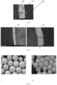
Fig. 8 ] est une image au microscope optique d'une coupe de bille selon l'invention montrant la bille de PSE support et les couches successives de cuivre, nickel chimique et d'or telle qu'obtenue à l'issue d'un premier mode de réalisation du procédé selon l'invention (bille de PSE d'environ 655 µm de diamètre et couche de cuivre de 17 µm d'épaisseur), - [
Fig. 9 ] montre une première image (A) prise au microscope optique d'une coupe de bille de PSE revêtue de cuivre telle qu'obtenue à l'issue de l'étape D) d'un deuxième mode de réalisation du procédé selon l'invention (bille de PSE de 660 µm de diamètre et couche de cuivre de 15 µm d'épaisseur), et une deuxième image (B) prise au microscope optique d'une coupe de bille de PSE revêtue de cuivre telle qu'obtenue à l'issue de l'étape D) d'un troisième mode de réalisation du procédé selon l'invention (bille de PSE de 630 µm de diamètre et couche de cuivre de 31 µm d'épaisseur), - [
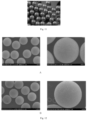
Fig. 10 ] montre une première image A prise au microscope optique montrant des billes support 10 en PSE présentant une distribution en taille D0 comprise entre 0.5 et 1 mm, et une deuxième image B prise au microscope optique montrant des billes support 10 en PSE obtenues après tri granulométrique sélectionnant des diamètres compris entre 0.63 et 0.66 mm. - [
Fig. 11 ] montre des billes 1 métallisées selon l'invention avec des diamètres de l'ordre de 400 µm +/-5%, - [
Fig. 12 ] est une image MEB montrant des billes 1 métallisées selon l'invention avant traitement thermique à 360°C (A) et une image MEB montrant des billes 1 métallisées selon le procédé de l'invention et ayant été soumises à un traitement thermique ultérieur à 360°C pendant 20 min (B) pour vérifier la tenue thermique des billes. - [
Fig. 13 ] est une image MEB montrant des billes avec un coeur en polystyrène dense qui ont été métallisées conformément aux étapes A à G du procédé selon l'invention, et ayant été soumises à un traitement thermique ultérieur à 360°C pendant 20 min (B) pour vérifier la tenue thermique des billes. - [
Fig. 1 ] est décrite dans la présentation de l'état de la technique connu. Elle montre en particulier des billes souples présentant des contacts à souder 1, 2 permettant facilement leur assemblage.Fig. 2 à Fig. 12 sont décrites plus en détail au niveau des exemples qui suivent, qui illustrent l'invention sans en limiter la portée. -
- dispositif de dépôt chimique auto-catalytique (pour le dépôt de cuivre et de nickel chimique) ;
- Dispositif de tamisage mécanique
-
- Billes de polystyrène expansé (PSE) de diamètre compris entre 595 µm et 665 µm ;
- Billes de polystyrène expansé (PSE) de diamètre de l'ordre de 400 µm,
- Nickel chimique (contenant 7 à 10 % en poids de P),
- Cuivre,
- Nitrate d'argent,
- Ions d'or.
- Les observations au microscope optique sont réalisées à l'aide d'un microscope optique, en surface ([
Fig. 4] à [Fig. 7 ]) et en coupe transversale ([Fig. 8] et [Fig. 9 ]). - Les observations des
figures 12 et13 sont obtenues à l'aide d'un microscope électronique à balayage (MEB). - Des billes de soudure selon l'invention sont élaborées à partir de billes de polystyrène expansé (PSE) selon un premier mode de réalisation du procédé selon l'invention. La fabrication est décomposée selon les étapes suivantes :
- 1) On procède à un premier tamisage mécanique de billes de PSE 10 ayant une distribution en taille comprise entre 0.5 et 1 mm pour ne conserver que les billes ayant un diamètre de l'ordre de 630 µm ([
Fig. 10 ]) ; - 2) Puis, on active la surface des grains de PSE afin de permettre une bonne accroche du traitement de métallisation ultérieur. La bille activée 10' est obtenue en déposant en surface des billes des germes d'argent. L'opération est menée en bain par réduction du nitrate d'argent. A l'issue de ce traitement, on obtient une bille 10' telle que montrée à [
Fig. 4 ]; - 3) La troisième étape consiste à réaliser le traitement de métallisation par du cuivre. Une couche de cuivre 110 de 30 µm d'épaisseur Ecu est obtenue par dépôt chimique auto-catalytique (cf. ([
Fig. 2], ([Fig. 3 ]). A l'issue de ce traitement, on obtient une bille 10" telle que montrée à [Fig. 5 ] (vue surfacique) ou à [Fig. 9 ], partie B (vue transversale) ; - La quatrième étape consiste à déposer une couche de nickel chimique (NiP) 111 de 5 µm d'épaisseur sur la couche de cuivre 110 (cf. [
Fig. 2], ([Fig. 3 ]). Ce revêtement est également réalisé par dépôt chimique auto-catalytique. A l'issue de ce traitement, on obtient une bille 10‴ telle que montrée à [Fig. 6 ] ; - La dernière couche de métallisation est une couche de finition 112 en Or (cf. [
Fig. 2 ]). Le dépôt est obtenu par déplacement galvanique par suite à une immersion des billes 10‴ revêtues de nickel chimique dans une solution contenant des ions Or. On dépose ainsi une couche d'or dont l'épaisseur EAu est comprise entre 0.05 µm et 0,12 µm (cf. [Fig. 2 ]). A l'issue de ce traitement, on obtient une bille de soudure 1 telle que montrée à [Fig. 7 ] ; - La dernière étape est un tri granulométrique des billes pour ne conserver que des billes selon l'invention 1 de diamètre Df de l'ordre de 700 µm +/-5%.
- On réalise des billes de soudure selon l'invention de la même manière qu'à l'exemple 1 avec des billes support de 660 µm de diamètre et un dépôt de cuivre de l'ordre de 15 à 17 µm d'épaisseur (cf.
figure 8 et 9A ). - On réalise des billes de soudure selon l'invention de la même manière qu'aux exemples 1 et 2, afin d'obtenir des billes de diamètre Df de l'ordre de 400 µm +/-5% (cf. [
Fig. 12 ]). - Les analyses MEB ([
Fig. 12 ]) montrent des billes métallisées et calibrées selon l'invention avant (12a) et après traitement thermique à 360°C (12b). On observe que les billes n'ont pas subi de dégradations/modifications suite au traitement thermique, démontrant leurs stabilités en température. - Afin d'établir une analyse comparative du poids des billes, 3 lots de billes (de diamètre D0 700 µm +/-5%) ont été réalisés selon les étapes A à G du procédé selon la présente invention (métallisation Cu/NiP/Au), puis soumises à un traitement thermique ultérieur à 360°C pendant 20 min (B) pour vérifier la tenue thermique des billes. Pour cela, on a utilisé 3 types de billes support différents :
- un premier lot réalisé à partir de billes en polystyrène expansé (présentant environ 95% de porosité),
- un deuxième lot réalisé à partir de billes en polystyrène réticulé (dense), et
- un troisième lot réalisé à partir de billes métallique en cuivre (dense).
- Pour chaque lot, 1000 billes ont été prélevées et pesées. On obtient les résultats suivants rassemblés dans le tableau 1 ci-après :
Tableau 1 Billes support Poids pour 1000 billes métallisées (g) Polystyrène expansé 0.225 Polystyrène dense 0.390 Cuivre dense 2.100 - Les billes réalisées selon la présente invention à partir de polystyrène expansé (premier lot) présentent un facteur de réduction de masse compris entre 1.7 et 9.4 comparé aux solutions actuelles (coeur dense en matière organique ou métallique).
- D'autre part, il a été remarqué que la stabilité thermique des billes est améliorée avec l'utilisation d'un coeur en PSE (billes selon l'invention du premier lot) comparativement aux billes obtenues à partir d'un coeur dense (billes des deuxième et troisième lots). En effet on constate qu'à partir de 360°C, les billes réalisées à partir de polystyrène dense (billes des deuxième et troisième lots) montrent un défaut de comportement avec l'apparition de « gouttelettes » de matière organique en surface des billes (
Figure 1 ). Le phénomène n'est pas observé sur les billes selon l'invention réalisées à partir de polystyrène expansé (billes du premier lot).
Claims (6)
- Procédé de fabrication de billes (1) de soudure composites métallisées en surface et calibrées de diamètre Df, lesdites billes (10) comprenant :- un coeur constitué par une particule support (10) de forme sphérique de diamètre D0, en polystyrène expansé (PSE) et présentant une porosité intragranulaire d'au moins 50%, et,- une enveloppe (11) recouvrant ladite particule support (10) et formée par une pluralité de couches superficielles métalliques (110, 111, 112), comprenant un revêtement de cuivre d'épaisseur Ecu, au moins une couche de nickel d'épaisseur ENi, et une couche de finition d'or d'une épaisseur EAu, ledit procédé étant caractérisé en ce qu'il comprend les étapes suivantes :A) une première étape de fourniture de particules support (10), suivie parB) une première étape de tri granulométrique des particules support (10), consistant en une étape de séparation physique et/ou mécanique des particules support (10) présentant un diamètre D0 tel que D0 = Df-2∗(ENi+ECu+EAu), D0 pouvant être choisi entre 200 µm et 1000 µm ;C) une étape de traitement d'activation des particules support (10) ainsi sélectionnées, pour obtenir des particules support activées (10') ;D) une première étape de métallisation desdites particules support activées (10') par dépôt chimique auto-catalytique d'une ou plusieurs couches de cuivre, cette étape étant répétée jusqu'à obtention d'un revêtement de cuivre d'épaisseur ECu de cuivre (110) comprise entre 15 et 30 µm, pour obtenir des particules support revêtues de cuivre (10") ;E) une deuxième étape de métallisation des particules support revêtues de cuivre (10") par dépôt chimique auto-catalytique d'au moins une couche de nickel allié à du phosphore NiP avec un pourcentage massique de 7 à 10% de phosphore par rapport au poids total de ladite couche de NiP, cette étape étant conduite jusqu'à obtention d'une épaisseur ENi de couche de nickel chimique (111) comprise entre 4 µm et 7 µm , pour obtenir des particules support revêtues de nickel chimique (10‴) ;F) une troisième étape de métallisation des particules support revêtues de nickel chimique (10‴) consistant en une étape de dépôt d'or par un procédé de déplacement galvanique réalisé par immersion dans une solution aqueuse contenant des ions d'or, de manière à obtenir des billes de soudure composites métallisées et revêtues en surface d'une couche de finition d'or d'une épaisseur EAu comprise entre 0,05 µm et 0,12 µm ; etG) une deuxième étape de tri granulométrique des particules ainsi métallisées pour trier et sélectionner des billes (1) de soudure composites métallisées en surface présentant un diamètre Df avec une tolérance de +/-5%.
- Procédé selon la revendication 1, dans lequel l'étape de tri granulométrique B) des particules support (10) consiste en un tamisage mécanique pour trier et sélectionner les particules support (10) présentant un diamètre D0 choisi entre 200 µm et 1000 µm.
- Procédé selon la revendication 2, dans lequel le tamisage mécanique B) des particules support (10) est suivi d'un traitement thermique à une température comprise entre 100°C et 120°C, et de préférence entre 110 °C et 120°C, de la tranche supérieure des particules ainsi triées dont la taille est supérieure à D0 +5%.
- Procédé selon l'une quelconque des revendications 1 à 3, dans lequel le traitement d'activation des particules support (10) sélectionnées consiste à déposer à leur surface des germes d'argent par introduction dans un bain de nitrate d'argent ou à déposer à leur surface du cuivre en couche mince inférieure ou égale à 1 µm, par dépôt physique en phase vapeur (PVD).
- Procédé selon l'une quelconque des revendications 1 à 4, comprenant en outre, entre les étapes D) et E), une étape de dissolution partielle ou totale du polystyrène expansé (PSE) constitutif des particules support (10), ou une étape de décomposition par voie thermique partielle ou totale du polystyrène expansé (PSE) constitutif des particules support (10).
- Utilisation des billes (10) de soudure composites métallisées en surface et calibrées de diamètre Df obtenues par le procédé tel que défini selon l'une quelconque des revendications 1 à 5, pour l'assemblage de cartes électroniques.
Applications Claiming Priority (2)
| Application Number | Priority Date | Filing Date | Title |
|---|---|---|---|
| FR1910055A FR3100822B1 (fr) | 2019-09-12 | 2019-09-12 | Billes de soudure composites metallisees en surface et calibrees pour l'assemblage de cartes electroniques |
| PCT/EP2020/075498 WO2021048374A1 (fr) | 2019-09-12 | 2020-09-11 | Billes de soudure composites metallisees en surface et calibrees pour l'assemblage de cartes electroniques |
Publications (3)
| Publication Number | Publication Date |
|---|---|
| EP4028576A1 EP4028576A1 (fr) | 2022-07-20 |
| EP4028576B1 true EP4028576B1 (fr) | 2023-11-01 |
| EP4028576C0 EP4028576C0 (fr) | 2023-11-01 |
Family
ID=70154438
Family Applications (1)
| Application Number | Title | Priority Date | Filing Date |
|---|---|---|---|
| EP20767856.6A Active EP4028576B1 (fr) | 2019-09-12 | 2020-09-11 | Billes de soudure composites metallisees en surface et calibrees pour l'assemblage de cartes electroniques |
Country Status (7)
| Country | Link |
|---|---|
| US (1) | US12030138B2 (fr) |
| EP (1) | EP4028576B1 (fr) |
| JP (1) | JP7560543B2 (fr) |
| KR (1) | KR102925927B1 (fr) |
| CN (1) | CN114599818B (fr) |
| FR (1) | FR3100822B1 (fr) |
| WO (1) | WO2021048374A1 (fr) |
Families Citing this family (2)
| Publication number | Priority date | Publication date | Assignee | Title |
|---|---|---|---|---|
| FR3100822B1 (fr) | 2019-09-12 | 2021-10-01 | Lifco Ind | Billes de soudure composites metallisees en surface et calibrees pour l'assemblage de cartes electroniques |
| CN120587747B (zh) * | 2025-07-18 | 2026-02-17 | 憬宏半导体(广东横琴)有限公司 | 一种复合焊料球、制备方法及堆叠封装结构 |
Family Cites Families (29)
| Publication number | Priority date | Publication date | Assignee | Title |
|---|---|---|---|---|
| US6336269B1 (en) * | 1993-11-16 | 2002-01-08 | Benjamin N. Eldridge | Method of fabricating an interconnection element |
| WO1997012718A1 (fr) * | 1995-10-06 | 1997-04-10 | Brown University Research Foundation | Procedes et compositions pour brasage |
| JPH10150263A (ja) * | 1996-11-19 | 1998-06-02 | Matsushita Electric Ind Co Ltd | 導電性ボールの搭載方法 |
| JP2001319994A (ja) * | 2000-02-29 | 2001-11-16 | Allied Material Corp | 半導体パッケージとその製造方法 |
| US6610591B1 (en) * | 2000-08-25 | 2003-08-26 | Micron Technology, Inc. | Methods of ball grid array |
| US6624500B2 (en) * | 2000-11-30 | 2003-09-23 | Kyocera Corporation | Thin-film electronic component and motherboard |
| JP3694249B2 (ja) | 2001-04-25 | 2005-09-14 | 積水化学工業株式会社 | 微粒子のめっき方法及び導電性微粒子及び接続構造体 |
| JP2003101207A (ja) | 2001-09-27 | 2003-04-04 | Nec Kyushu Ltd | 半田ボールおよびそれを用いた部品接続構造 |
| US6587345B2 (en) * | 2001-11-09 | 2003-07-01 | International Business Machines Corporation | Electronic device substrate assembly with impermeable barrier and method of making |
| JP2005200728A (ja) * | 2004-01-16 | 2005-07-28 | Mitsui Mining & Smelting Co Ltd | 二層コート粒子粉末の製造方法及びその製造方法で得られた二層コート粒子粉末 |
| DE102004005668B4 (de) * | 2004-02-05 | 2021-09-16 | Snaptrack, Inc. | Elektrisches Bauelement und Herstellungsverfahren |
| WO2006103976A1 (fr) * | 2005-03-25 | 2006-10-05 | Dai Nippon Printing Co., Ltd. | Composition d'encre pour jet d'encre pour un filtre coloré, procédé servant à produire un filtre coloré et filtre coloré |
| JP2007044718A (ja) * | 2005-08-09 | 2007-02-22 | Millenium Gate Technology Co Ltd | 金属ボール、金属ボールの作製方法、めっき構造物および半田付け方法 |
| KR100719802B1 (ko) * | 2005-12-28 | 2007-05-18 | 제일모직주식회사 | 이방 전도 접속용 고신뢰성 전도성 미립자 |
| JP2007239084A (ja) * | 2006-03-13 | 2007-09-20 | Toyota Motor Corp | 無電解めっき方法 |
| CN101245148B (zh) * | 2007-02-13 | 2012-05-23 | 镇江爱邦电子科技有限公司 | 单分散性高性能导电银颗粒 |
| JP4364928B2 (ja) * | 2007-04-13 | 2009-11-18 | 積水化学工業株式会社 | 導電性微粒子、異方性導電材料及び導電接続構造体 |
| EP2139009B1 (fr) * | 2007-04-13 | 2013-06-26 | Sekisui Chemical Co., Ltd. | Particules fines electroconductrices, materiau anisotrope electroconducteur et structure de connexion electroconductrice |
| KR100892301B1 (ko) * | 2007-04-23 | 2009-04-08 | 한화석유화학 주식회사 | 환원 및 치환금도금 방법을 이용한 도전볼 제조 |
| US20140099472A1 (en) * | 2008-08-11 | 2014-04-10 | Greenhill Antiballistics Corporation | Composite material |
| JP4746116B2 (ja) * | 2008-10-14 | 2011-08-10 | 日本化学工業株式会社 | 導電性粉体及びそれを含む導電性材料並びに導電性粒子の製造方法 |
| US8267255B2 (en) * | 2009-09-07 | 2012-09-18 | Optnics Precision Co., Ltd. | Sieve, sifting device, solder balls, and method of sifting spherical particles |
| US9721912B2 (en) * | 2011-11-02 | 2017-08-01 | Maxim Integrated Products, Inc. | Wafer-level chip-scale package device having bump assemblies configured to furnish shock absorber functionality |
| JP5580954B1 (ja) * | 2013-02-28 | 2014-08-27 | 積水化学工業株式会社 | 導電性微粒子、異方性導電材料、及び、導電接続構造体 |
| US20160244891A1 (en) * | 2015-02-25 | 2016-08-25 | Mk Electron Co., Ltd. | Solder ball for fluxless bonding, method of manufacturing the same, and method of forming solder bump |
| JP6500583B2 (ja) * | 2015-05-11 | 2019-04-17 | 日立化成株式会社 | 導電粒子、及び導電粒子を用いた半導体パッケージ |
| KR101877931B1 (ko) * | 2016-12-06 | 2018-07-12 | 주식회사 테토스 | 솔더 입자의 제조 방법 |
| FR3100822B1 (fr) | 2019-09-12 | 2021-10-01 | Lifco Ind | Billes de soudure composites metallisees en surface et calibrees pour l'assemblage de cartes electroniques |
| JP6892621B1 (ja) * | 2020-09-10 | 2021-06-23 | 千住金属工業株式会社 | 核材料、電子部品及びバンプ電極の形成方法 |
-
2019
- 2019-09-12 FR FR1910055A patent/FR3100822B1/fr active Active
-
2020
- 2020-09-11 CN CN202080060917.4A patent/CN114599818B/zh active Active
- 2020-09-11 KR KR1020227010468A patent/KR102925927B1/ko active Active
- 2020-09-11 EP EP20767856.6A patent/EP4028576B1/fr active Active
- 2020-09-11 US US17/642,617 patent/US12030138B2/en active Active
- 2020-09-11 JP JP2022515075A patent/JP7560543B2/ja active Active
- 2020-09-11 WO PCT/EP2020/075498 patent/WO2021048374A1/fr not_active Ceased
Also Published As
| Publication number | Publication date |
|---|---|
| WO2021048374A1 (fr) | 2021-03-18 |
| CN114599818B (zh) | 2024-10-15 |
| JP2023505403A (ja) | 2023-02-09 |
| KR20220074882A (ko) | 2022-06-03 |
| KR102925927B1 (ko) | 2026-02-12 |
| CN114599818A (zh) | 2022-06-07 |
| US12030138B2 (en) | 2024-07-09 |
| EP4028576A1 (fr) | 2022-07-20 |
| JP7560543B2 (ja) | 2024-10-02 |
| US20220339742A1 (en) | 2022-10-27 |
| FR3100822A1 (fr) | 2021-03-19 |
| FR3100822B1 (fr) | 2021-10-01 |
| EP4028576C0 (fr) | 2023-11-01 |
Similar Documents
| Publication | Publication Date | Title |
|---|---|---|
| EP2053646A1 (fr) | Procede d'interconnexion verticale au sein de modules electroniques 3D utilisant des vias | |
| WO2021048374A1 (fr) | Billes de soudure composites metallisees en surface et calibrees pour l'assemblage de cartes electroniques | |
| EP2727144B1 (fr) | Procédé d'hybridation d'un composant muni d'inserts creux | |
| EP2365741B1 (fr) | Procede de metallisation de vias borgnes | |
| EP2463924B1 (fr) | Dépôt de matériaux thermoélectriques par impression | |
| WO2013019541A4 (fr) | Trous d'interconnexion à faible contrainte | |
| FR2645337A1 (fr) | Procede de formation de terminaisons de condensateurs ceramiques a faible inductance par des techniques de pellicules minces, et condensateur obtenu | |
| EP3078436B1 (fr) | Procédé de fabrication d'un composant horloger | |
| EP3324435B1 (fr) | Procede de realisation de vias sur substrat flexible | |
| EP3796102A1 (fr) | Procede de fabrication d'un balancier pour piece d'horlogerie | |
| FR2766618A1 (fr) | Procede de fabrication d'un film conducteur anisotrope a inserts conducteurs | |
| EP2223581B1 (fr) | Procédé de réalisation d'une interconnexion électrique entre deux couches conductrices | |
| FR2575332A1 (fr) | Dispositif semi-conducteur ayant une couche metallisee de plusieurs epaisseurs et procede pour sa fabrication | |
| JP7525612B2 (ja) | 回路基板およびその製造方法 | |
| EP2791969B1 (fr) | Formation d'une connexion electrique du type via | |
| EP1756864B9 (fr) | Procede de fabrication de puces | |
| EP1993129B1 (fr) | Procédé de frabrication de cavités d'air utilisant des nanotubes | |
| FR3082033A1 (fr) | Procede de fabrication d'un calculateur a reseaux de neurones recurrents | |
| EP3822709B1 (fr) | Procédé de fabrication d'un composant horloger | |
| WO2023118393A1 (fr) | Procede de fabrication d'une piece multi-materiaux polymere et metallique et/ou dielectrique | |
| KR20230099075A (ko) | 복합금속 나노입자의 제조방법 및 이를 통해 제조된 복합금속 나노입자 | |
| EP2543625A1 (fr) | Procédé de réalisation d'un insert métallique dans une pièce horlogère | |
| EP2884532B1 (fr) | Procédé de fabrication d'un organe électriquement conducteur pour composant électronique présentant une extrémité munie d'une cavité | |
| KR102465663B1 (ko) | 입자 크기 제어를 통한 금속 나노입자층 제조방법 | |
| FR2996053A1 (fr) | Procede d'assemblage de deux composants electroniques, de type flip-chip, assemblage obtenu selon le procede. |
Legal Events
| Date | Code | Title | Description |
|---|---|---|---|
| STAA | Information on the status of an ep patent application or granted ep patent |
Free format text: STATUS: UNKNOWN |
|
| STAA | Information on the status of an ep patent application or granted ep patent |
Free format text: STATUS: THE INTERNATIONAL PUBLICATION HAS BEEN MADE |
|
| PUAI | Public reference made under article 153(3) epc to a published international application that has entered the european phase |
Free format text: ORIGINAL CODE: 0009012 |
|
| STAA | Information on the status of an ep patent application or granted ep patent |
Free format text: STATUS: REQUEST FOR EXAMINATION WAS MADE |
|
| 17P | Request for examination filed |
Effective date: 20220224 |
|
| AK | Designated contracting states |
Kind code of ref document: A1 Designated state(s): AL AT BE BG CH CY CZ DE DK EE ES FI FR GB GR HR HU IE IS IT LI LT LU LV MC MK MT NL NO PL PT RO RS SE SI SK SM TR |
|
| DAV | Request for validation of the european patent (deleted) | ||
| DAX | Request for extension of the european patent (deleted) | ||
| GRAP | Despatch of communication of intention to grant a patent |
Free format text: ORIGINAL CODE: EPIDOSNIGR1 |
|
| STAA | Information on the status of an ep patent application or granted ep patent |
Free format text: STATUS: GRANT OF PATENT IS INTENDED |
|
| RIC1 | Information provided on ipc code assigned before grant |
Ipc: B23K 35/02 20060101ALI20230214BHEP Ipc: C23C 18/20 20060101ALI20230214BHEP Ipc: C23C 18/32 20060101ALI20230214BHEP Ipc: C23C 18/38 20060101ALI20230214BHEP Ipc: C23C 18/54 20060101ALI20230214BHEP Ipc: C23C 18/16 20060101AFI20230214BHEP |
|
| INTG | Intention to grant announced |
Effective date: 20230306 |
|
| GRAJ | Information related to disapproval of communication of intention to grant by the applicant or resumption of examination proceedings by the epo deleted |
Free format text: ORIGINAL CODE: EPIDOSDIGR1 |
|
| STAA | Information on the status of an ep patent application or granted ep patent |
Free format text: STATUS: REQUEST FOR EXAMINATION WAS MADE |
|
| GRAP | Despatch of communication of intention to grant a patent |
Free format text: ORIGINAL CODE: EPIDOSNIGR1 |
|
| STAA | Information on the status of an ep patent application or granted ep patent |
Free format text: STATUS: GRANT OF PATENT IS INTENDED |
|
| INTC | Intention to grant announced (deleted) | ||
| INTG | Intention to grant announced |
Effective date: 20230623 |
|
| RAP1 | Party data changed (applicant data changed or rights of an application transferred) |
Owner name: INSTITUT DE RECHERCHES EN INGENIERIE DES SURFACES |
|
| RAP1 | Party data changed (applicant data changed or rights of an application transferred) |
Owner name: "INSTITUT DE RECHERCHES EN INGENIERIE DES SURFACES" |
|
| GRAS | Grant fee paid |
Free format text: ORIGINAL CODE: EPIDOSNIGR3 |
|
| GRAA | (expected) grant |
Free format text: ORIGINAL CODE: 0009210 |
|
| STAA | Information on the status of an ep patent application or granted ep patent |
Free format text: STATUS: THE PATENT HAS BEEN GRANTED |
|
| AK | Designated contracting states |
Kind code of ref document: B1 Designated state(s): AL AT BE BG CH CY CZ DE DK EE ES FI FR GB GR HR HU IE IS IT LI LT LU LV MC MK MT NL NO PL PT RO RS SE SI SK SM TR |
|
| REG | Reference to a national code |
Ref country code: GB Ref legal event code: FG4D Free format text: NOT ENGLISH |
|
| REG | Reference to a national code |
Ref country code: CH Ref legal event code: EP |
|
| REG | Reference to a national code |
Ref country code: IE Ref legal event code: FG4D Free format text: LANGUAGE OF EP DOCUMENT: FRENCH |
|
| REG | Reference to a national code |
Ref country code: DE Ref legal event code: R096 Ref document number: 602020020320 Country of ref document: DE |
|
| U01 | Request for unitary effect filed |
Effective date: 20231128 |
|
| U07 | Unitary effect registered |
Designated state(s): AT BE BG DE DK EE FI FR IT LT LU LV MT NL PT SE SI Effective date: 20231204 |
|
| PG25 | Lapsed in a contracting state [announced via postgrant information from national office to epo] |
Ref country code: GR Free format text: LAPSE BECAUSE OF FAILURE TO SUBMIT A TRANSLATION OF THE DESCRIPTION OR TO PAY THE FEE WITHIN THE PRESCRIBED TIME-LIMIT Effective date: 20240202 |
|
| PG25 | Lapsed in a contracting state [announced via postgrant information from national office to epo] |
Ref country code: IS Free format text: LAPSE BECAUSE OF FAILURE TO SUBMIT A TRANSLATION OF THE DESCRIPTION OR TO PAY THE FEE WITHIN THE PRESCRIBED TIME-LIMIT Effective date: 20240301 |
|
| PG25 | Lapsed in a contracting state [announced via postgrant information from national office to epo] |
Ref country code: ES Free format text: LAPSE BECAUSE OF FAILURE TO SUBMIT A TRANSLATION OF THE DESCRIPTION OR TO PAY THE FEE WITHIN THE PRESCRIBED TIME-LIMIT Effective date: 20231101 |
|
| PG25 | Lapsed in a contracting state [announced via postgrant information from national office to epo] |
Ref country code: IS Free format text: LAPSE BECAUSE OF FAILURE TO SUBMIT A TRANSLATION OF THE DESCRIPTION OR TO PAY THE FEE WITHIN THE PRESCRIBED TIME-LIMIT Effective date: 20240301 Ref country code: GR Free format text: LAPSE BECAUSE OF FAILURE TO SUBMIT A TRANSLATION OF THE DESCRIPTION OR TO PAY THE FEE WITHIN THE PRESCRIBED TIME-LIMIT Effective date: 20240202 Ref country code: ES Free format text: LAPSE BECAUSE OF FAILURE TO SUBMIT A TRANSLATION OF THE DESCRIPTION OR TO PAY THE FEE WITHIN THE PRESCRIBED TIME-LIMIT Effective date: 20231101 |
|
| PG25 | Lapsed in a contracting state [announced via postgrant information from national office to epo] |
Ref country code: RS Free format text: LAPSE BECAUSE OF FAILURE TO SUBMIT A TRANSLATION OF THE DESCRIPTION OR TO PAY THE FEE WITHIN THE PRESCRIBED TIME-LIMIT Effective date: 20231101 Ref country code: PL Free format text: LAPSE BECAUSE OF FAILURE TO SUBMIT A TRANSLATION OF THE DESCRIPTION OR TO PAY THE FEE WITHIN THE PRESCRIBED TIME-LIMIT Effective date: 20231101 Ref country code: NO Free format text: LAPSE BECAUSE OF FAILURE TO SUBMIT A TRANSLATION OF THE DESCRIPTION OR TO PAY THE FEE WITHIN THE PRESCRIBED TIME-LIMIT Effective date: 20240201 Ref country code: HR Free format text: LAPSE BECAUSE OF FAILURE TO SUBMIT A TRANSLATION OF THE DESCRIPTION OR TO PAY THE FEE WITHIN THE PRESCRIBED TIME-LIMIT Effective date: 20231101 |
|
| PG25 | Lapsed in a contracting state [announced via postgrant information from national office to epo] |
Ref country code: CZ Free format text: LAPSE BECAUSE OF FAILURE TO SUBMIT A TRANSLATION OF THE DESCRIPTION OR TO PAY THE FEE WITHIN THE PRESCRIBED TIME-LIMIT Effective date: 20231101 |
|
| PG25 | Lapsed in a contracting state [announced via postgrant information from national office to epo] |
Ref country code: SK Free format text: LAPSE BECAUSE OF FAILURE TO SUBMIT A TRANSLATION OF THE DESCRIPTION OR TO PAY THE FEE WITHIN THE PRESCRIBED TIME-LIMIT Effective date: 20231101 |
|
| PG25 | Lapsed in a contracting state [announced via postgrant information from national office to epo] |
Ref country code: SM Free format text: LAPSE BECAUSE OF FAILURE TO SUBMIT A TRANSLATION OF THE DESCRIPTION OR TO PAY THE FEE WITHIN THE PRESCRIBED TIME-LIMIT Effective date: 20231101 Ref country code: SK Free format text: LAPSE BECAUSE OF FAILURE TO SUBMIT A TRANSLATION OF THE DESCRIPTION OR TO PAY THE FEE WITHIN THE PRESCRIBED TIME-LIMIT Effective date: 20231101 Ref country code: CZ Free format text: LAPSE BECAUSE OF FAILURE TO SUBMIT A TRANSLATION OF THE DESCRIPTION OR TO PAY THE FEE WITHIN THE PRESCRIBED TIME-LIMIT Effective date: 20231101 |
|
| REG | Reference to a national code |
Ref country code: DE Ref legal event code: R097 Ref document number: 602020020320 Country of ref document: DE |
|
| PLBE | No opposition filed within time limit |
Free format text: ORIGINAL CODE: 0009261 |
|
| STAA | Information on the status of an ep patent application or granted ep patent |
Free format text: STATUS: NO OPPOSITION FILED WITHIN TIME LIMIT |
|
| 26N | No opposition filed |
Effective date: 20240802 |
|
| U20 | Renewal fee for the european patent with unitary effect paid |
Year of fee payment: 5 Effective date: 20240925 |
|
| PG25 | Lapsed in a contracting state [announced via postgrant information from national office to epo] |
Ref country code: MC Free format text: LAPSE BECAUSE OF FAILURE TO SUBMIT A TRANSLATION OF THE DESCRIPTION OR TO PAY THE FEE WITHIN THE PRESCRIBED TIME-LIMIT Effective date: 20231101 |
|
| REG | Reference to a national code |
Ref country code: CH Ref legal event code: PL |
|
| PG25 | Lapsed in a contracting state [announced via postgrant information from national office to epo] |
Ref country code: CH Free format text: LAPSE BECAUSE OF NON-PAYMENT OF DUE FEES Effective date: 20240930 |
|
| PG25 | Lapsed in a contracting state [announced via postgrant information from national office to epo] |
Ref country code: IE Free format text: LAPSE BECAUSE OF NON-PAYMENT OF DUE FEES Effective date: 20240911 |
|
| PGFP | Annual fee paid to national office [announced via postgrant information from national office to epo] |
Ref country code: GB Payment date: 20250923 Year of fee payment: 6 |
|
| U20 | Renewal fee for the european patent with unitary effect paid |
Year of fee payment: 6 Effective date: 20250923 |
|
| PG25 | Lapsed in a contracting state [announced via postgrant information from national office to epo] |
Ref country code: RO Free format text: LAPSE BECAUSE OF FAILURE TO SUBMIT A TRANSLATION OF THE DESCRIPTION OR TO PAY THE FEE WITHIN THE PRESCRIBED TIME-LIMIT Effective date: 20231101 |
|
| PG25 | Lapsed in a contracting state [announced via postgrant information from national office to epo] |
Ref country code: CY Free format text: LAPSE BECAUSE OF FAILURE TO SUBMIT A TRANSLATION OF THE DESCRIPTION OR TO PAY THE FEE WITHIN THE PRESCRIBED TIME-LIMIT; INVALID AB INITIO Effective date: 20200911 |
|
| PG25 | Lapsed in a contracting state [announced via postgrant information from national office to epo] |
Ref country code: HU Free format text: LAPSE BECAUSE OF FAILURE TO SUBMIT A TRANSLATION OF THE DESCRIPTION OR TO PAY THE FEE WITHIN THE PRESCRIBED TIME-LIMIT; INVALID AB INITIO Effective date: 20200911 |
|
| U1N | Appointed representative for the unitary patent procedure changed after the registration of the unitary effect |
Representative=s name: NOVAGRAAF TECHNOLOGIES; FR |