EP4002437A1 - Kontaktfensterstruktur, metallstecker und herstellungsverfahren dafür sowie halbleiterstruktur - Google Patents
Kontaktfensterstruktur, metallstecker und herstellungsverfahren dafür sowie halbleiterstruktur Download PDFInfo
- Publication number
- EP4002437A1 EP4002437A1 EP21773256.9A EP21773256A EP4002437A1 EP 4002437 A1 EP4002437 A1 EP 4002437A1 EP 21773256 A EP21773256 A EP 21773256A EP 4002437 A1 EP4002437 A1 EP 4002437A1
- Authority
- EP
- European Patent Office
- Prior art keywords
- layer
- forming
- contact window
- annular pad
- dielectric layer
- Prior art date
- Legal status (The legal status is an assumption and is not a legal conclusion. Google has not performed a legal analysis and makes no representation as to the accuracy of the status listed.)
- Granted
Links
Images




Classifications
-
- H—ELECTRICITY
- H10—SEMICONDUCTOR DEVICES; ELECTRIC SOLID-STATE DEVICES NOT OTHERWISE PROVIDED FOR
- H10W—GENERIC PACKAGES, INTERCONNECTIONS, CONNECTORS OR OTHER CONSTRUCTIONAL DETAILS OF DEVICES COVERED BY CLASS H10
- H10W20/00—Interconnections in chips, wafers or substrates
- H10W20/01—Manufacture or treatment
- H10W20/031—Manufacture or treatment of conductive parts of the interconnections
- H10W20/069—Manufacture or treatment of conductive parts of the interconnections by forming self-aligned vias or self-aligned contact plugs
- H10W20/0696—Manufacture or treatment of conductive parts of the interconnections by forming self-aligned vias or self-aligned contact plugs by using sacrificial placeholders, e.g. using sacrificial plugs
-
- H—ELECTRICITY
- H10—SEMICONDUCTOR DEVICES; ELECTRIC SOLID-STATE DEVICES NOT OTHERWISE PROVIDED FOR
- H10W—GENERIC PACKAGES, INTERCONNECTIONS, CONNECTORS OR OTHER CONSTRUCTIONAL DETAILS OF DEVICES COVERED BY CLASS H10
- H10W20/00—Interconnections in chips, wafers or substrates
- H10W20/01—Manufacture or treatment
- H10W20/071—Manufacture or treatment of dielectric parts thereof
- H10W20/081—Manufacture or treatment of dielectric parts thereof by forming openings in the dielectric parts
-
- H—ELECTRICITY
- H10—SEMICONDUCTOR DEVICES; ELECTRIC SOLID-STATE DEVICES NOT OTHERWISE PROVIDED FOR
- H10W—GENERIC PACKAGES, INTERCONNECTIONS, CONNECTORS OR OTHER CONSTRUCTIONAL DETAILS OF DEVICES COVERED BY CLASS H10
- H10W20/00—Interconnections in chips, wafers or substrates
- H10W20/01—Manufacture or treatment
- H10W20/071—Manufacture or treatment of dielectric parts thereof
- H10W20/081—Manufacture or treatment of dielectric parts thereof by forming openings in the dielectric parts
- H10W20/082—Manufacture or treatment of dielectric parts thereof by forming openings in the dielectric parts the openings being tapered via holes
-
- H—ELECTRICITY
- H10—SEMICONDUCTOR DEVICES; ELECTRIC SOLID-STATE DEVICES NOT OTHERWISE PROVIDED FOR
- H10W—GENERIC PACKAGES, INTERCONNECTIONS, CONNECTORS OR OTHER CONSTRUCTIONAL DETAILS OF DEVICES COVERED BY CLASS H10
- H10W20/00—Interconnections in chips, wafers or substrates
- H10W20/01—Manufacture or treatment
- H10W20/071—Manufacture or treatment of dielectric parts thereof
- H10W20/081—Manufacture or treatment of dielectric parts thereof by forming openings in the dielectric parts
- H10W20/089—Manufacture or treatment of dielectric parts thereof by forming openings in the dielectric parts using processes for implementing desired shapes or dispositions of the openings, e.g. double patterning
-
- H—ELECTRICITY
- H10—SEMICONDUCTOR DEVICES; ELECTRIC SOLID-STATE DEVICES NOT OTHERWISE PROVIDED FOR
- H10W—GENERIC PACKAGES, INTERCONNECTIONS, CONNECTORS OR OTHER CONSTRUCTIONAL DETAILS OF DEVICES COVERED BY CLASS H10
- H10W20/00—Interconnections in chips, wafers or substrates
- H10W20/40—Interconnections external to wafers or substrates, e.g. back-end-of-line [BEOL] metallisations or vias connecting to gate electrodes
- H10W20/41—Interconnections external to wafers or substrates, e.g. back-end-of-line [BEOL] metallisations or vias connecting to gate electrodes characterised by their conductive parts
- H10W20/42—Vias, e.g. via plugs
-
- H—ELECTRICITY
- H10—SEMICONDUCTOR DEVICES; ELECTRIC SOLID-STATE DEVICES NOT OTHERWISE PROVIDED FOR
- H10W—GENERIC PACKAGES, INTERCONNECTIONS, CONNECTORS OR OTHER CONSTRUCTIONAL DETAILS OF DEVICES COVERED BY CLASS H10
- H10W20/00—Interconnections in chips, wafers or substrates
- H10W20/40—Interconnections external to wafers or substrates, e.g. back-end-of-line [BEOL] metallisations or vias connecting to gate electrodes
- H10W20/41—Interconnections external to wafers or substrates, e.g. back-end-of-line [BEOL] metallisations or vias connecting to gate electrodes characterised by their conductive parts
- H10W20/435—Cross-sectional shapes or dispositions of interconnections
-
- H—ELECTRICITY
- H10—SEMICONDUCTOR DEVICES; ELECTRIC SOLID-STATE DEVICES NOT OTHERWISE PROVIDED FOR
- H10W—GENERIC PACKAGES, INTERCONNECTIONS, CONNECTORS OR OTHER CONSTRUCTIONAL DETAILS OF DEVICES COVERED BY CLASS H10
- H10W20/00—Interconnections in chips, wafers or substrates
- H10W20/01—Manufacture or treatment
- H10W20/071—Manufacture or treatment of dielectric parts thereof
- H10W20/074—Manufacture or treatment of dielectric parts thereof of dielectric parts comprising thin functional dielectric layers, e.g. dielectric etch-stop, barrier, capping or liner layers
- H10W20/076—Manufacture or treatment of dielectric parts thereof of dielectric parts comprising thin functional dielectric layers, e.g. dielectric etch-stop, barrier, capping or liner layers in via holes or trenches
- H10W20/0765—Manufacture or treatment of dielectric parts thereof of dielectric parts comprising thin functional dielectric layers, e.g. dielectric etch-stop, barrier, capping or liner layers in via holes or trenches the thin functional dielectric layers being temporary, e.g. sacrificial layers
-
- H—ELECTRICITY
- H10—SEMICONDUCTOR DEVICES; ELECTRIC SOLID-STATE DEVICES NOT OTHERWISE PROVIDED FOR
- H10W—GENERIC PACKAGES, INTERCONNECTIONS, CONNECTORS OR OTHER CONSTRUCTIONAL DETAILS OF DEVICES COVERED BY CLASS H10
- H10W20/00—Interconnections in chips, wafers or substrates
- H10W20/40—Interconnections external to wafers or substrates, e.g. back-end-of-line [BEOL] metallisations or vias connecting to gate electrodes
- H10W20/41—Interconnections external to wafers or substrates, e.g. back-end-of-line [BEOL] metallisations or vias connecting to gate electrodes characterised by their conductive parts
- H10W20/425—Barrier, adhesion or liner layers
Definitions
- the disclosure relates to the field of semiconductor, and in particular to a contact window structure, a metal plug and a forming method thereof, and a semiconductor structure.
- the design of two or more layers of multi-layer metal interconnecting wires has become a commonly used method in the super large-scale integrated circuit technology.
- the conduction between different metal layers or between a metal layer and a pad layer can be realized by a metal plug.
- the depth-to-width ratio of vias formed in the process of forming the metal plug continues to increase, which leads to compromised performance relative to the circuit requirements proposed by the designer.
- a technical problem to be solved by embodiments of the disclosure is to provide a contact window structure, a metal plug and a forming method thereof to reduce a phenomenon that a critical size of a bottom of a via is greater than a critical size of a top of the via, and overcome the problem that a size of the via slightly shrinks in an etching process.
- Embodiments of the disclosure provide a forming method of a contact window structure, which may include:
- forming the annular pad may include:
- forming the annular pad may include:
- the method may further include: after forming the annular pad, removing the mask material layer to form a dielectric layer on the target layer and the annular pad, or after forming the annular pad, retaining the mask material layer and forming a dielectric layer on the mask material layer.
- the central via in the middle part of the annular pad is fully filled with the formed dielectric layer.
- the central via is partially filled or not filled with the dielectric layer, and an air gap is formed in the annular pad.
- the method may further include: before forming the dielectric layer, filling the central via in the middle part of the annular pad with a sacrificial layer, wherein in etching the dielectric layer to form the etch hole, an etching rate for the sacrificial layer is greater than an etching rate for the dielectric layer.
- a thickness of the annular pad may be 3 times or more of a size of the central via.
- the target layer in a process of forming the contact window, is partially removed by etching.
- the method may further include: providing a substrate, the target layer may be formed in the substrate, and a surface of the target layer is exposed from the substrate.
- the embodiments of the disclosure further provide a method of forming a metal plug, which may include:
- the embodiments of the disclosure further provide a contact window structure, which may include:
- the embodiments of the disclosure further provide a semiconductor structure, which may include:
- a metal plug which may include:
- a target layer is provided; an annular pad is formed on a surface of the target layer, a central via, from which partial surface of the target layer is exposed, in the middle part of the annular pad; a dielectric layer covering the target layer and the annular pad is formed; the dielectric layer is etched to form an etch hole connected to the central via in the dielectric layer; and the annular pad is removed to form the contact window structure.
- a size of the central via may be enlarged, so that a size of a bottom of the contact window structure may be enlarged; and in forming the metal plug in the contact window structure, a contact area between a bottom of the metal plug and the target layer may be increased, and a contact resistance between the bottom of the metal plug and the target layer is reduced.
- a depth or depth-to-width ratio of the etch hole formed in the dielectric layer may be reduced, so that the difficulty of forming hole etching is reduced, and therefore, there is no need to increase the size of the etch hole to form the etch hole, or the size of the etch hole may even be reduced to improve the integration, that is, a size of a top of the formed contact window structure may be the same as or smaller than a size of a top formed according to a related technology, while the size of the bottom of the formed contact window structure is increased.
- a process of forming the annular pad may include: forming a columnar structure on the partial surface of the target layer; forming a pad material layer on a side wall and a top surface of the columnar structure as well as the partial surface of the target layer; removing the pad material layer on the top surface of the columnar structure and the partial surface of the target layer by etching without a mask, to form the annular pad on a surface of the side wall of the columnar structure; and removing the columnar structure after forming the annular pad.
- the annular pad formed by such method has high precision in size and shape, and has a relative high side wall morphology.
- the process of forming the annular pad may include: forming a mask material layer on a substrate and the partial surface of the target layer, a first via, from which the partial surface of the target layer is exposed, is formed in the mask material layer; forming a pad material layer on a side wall and a bottom surface of the first via as well as a surface of the mask material layer; and removing the pad material layer on the surface of the mask material layer and the bottom surface of the first via by etching without a mask, to form the annular pad on a surface of the side wall of the first via.
- the annular pad formed by such method has high precision in size and shape, and has a relative high side wall morphology.
- the size of the bottom of the contact window structure may be enlarged; and in forming the metal plug in the contact window structure, the contact area between the bottom of the metal plug and the target layer may be increased, and the contact resistance between the bottom of the metal plug and the target layer is reduced.
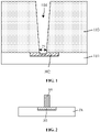
- the process of forming a metal plug in the related technology includes the following steps.
- a target metal layer 102 is formed in a substrate 101, and the target metal layer 102 is flush with a surface of the substrate 101.
- a dielectric layer 103 is formed on the substrate 101 and the target metal layer 102.
- a via (or a contact window structure) 104 is formed in the dielectric layer 103.
- the via (or the contact window structure) is filled with metal (not shown in the figure) to form the metal plug (not shown in the figure).
- a depth-to-width ratio of vias formed in the dielectric layer continues to increase, and the via with high depth-to-width ratio is a big challenge for the etching process.
- the via gradually narrows, and a critical size 21 of a bottom of the via 104 is smaller than a critical size of a top of the via 104.
- the window size in the bottom layer of the via usually limit a resistance value of the whole contact window, and the slightly shrunk size may greatly reduce the contact area with the target metal layer.
- a slight shrink phenomena may occur in the existing process for forming the via, especially for the via with a high depth-to-width ratio, and this phenomena results in that the size of the bottom of the via is smaller than that of the top of the via, and the contact resistance is increased.
- the embodiments of the disclosure provide a contact window structure, a metal plug and a forming method thereof, as well as a semiconductor structure.
- the method of forming the contact window structure includes the following steps. A target layer is provided. An annular pad is formed on a surface of the target layer, and a central via, from which partial surface of the target layer is exposed, in the middle part of the annular pad. A dielectric layer covering the target layer and the annular pad is formed. The dielectric layer is etched to form an etch hole connected to the central via in the dielectric layer. The annular pad is removed to form the contact window structure.
- a size of the central via may be enlarged, so that a size of a bottom of the contact window structure may be enlarged; and in forming the metal plug in the contact window structure, a contact area between a bottom of the metal plug and the target layer may be increased, and a contact resistance between the two is reduced.
- a depth or depth-to-width ratio of the etch hole formed in the dielectric layer may be reduced, so that the difficulty in forming hole etching is reduced, and therefore, in forming the etch hole, there is no need to increase the size of the etch hole or even may reduce the size of the etch hole to improve the integration, that is, a size of a top of the formed contact window structure may be the same as or smaller than a size of a top formed according to the related technology, while the size of the bottom of the formed contact window structure is increased.
- the schematic diagrams will not be partially enlarged according to a general scale, and the schematic diagrams are only examples, which should not limit the protection scope of the embodiments of the present disclosure herein. Respective to describing the embodiments of the disclosure in detail, for ease of description, the schematic diagrams will be partially enlarged at a non-normal scale, and the schematic diagrams are only examples, which should not limit the protection scope of the embodiments of the disclosure herein. Furthermore, a three-dimensional space size of length, width and depth should be included in practical manufacturing.
- a substrate 201 is provided.
- a target layer 202 is formed in the substrate 201, and the substrate 201 exposes a surface of the target layer 202.
- the substrate 201 may be a semiconductor substrate.
- the target layer 202 may be a doped region (for example, a region doped with N-type impurity ions or doped with P-type impurity ions) located in the semiconductor substrate or a metal silicide region (for example, a nickel silicide region or a cobalt silicide region) located in the semiconductor substrate.
- the semiconductor substrate may be made of silicon (Si), germanium (Ge) or silicon-germanium (GeSi), silicon carbide (SiC); or may be Silicon-on-Insulator (SOI), Germanium-on-Insulator (GOI); or may be other materials, for example, group III-V compounds such as gallium arsenide.
- the substrate 201 may include the semiconductor substrate and an interlevel dielectric layer located on the semiconductor substrate, and the target layer 202 is located in the interlevel dielectric layer.
- the interlevel dielectric layer may has a monolayer or multilayer stack structure
- the target layer 202 may be a metal layer
- the metal layer may be connected with a conductive structure (for example, a conductive plug) formed in the lower dielectric layer.
- the surface of the target layer 202 may be flush with a surface of the substrate 201, or is slightly higher than the surface of the substrate 102.
- target layers 202 There may be one or more (greater than or equal to 2) target layers 202 formed in the substrate 201. When there are multiple target layers 202, adjacent target layers are separated from each other.
- the substrate 201 with only one target layer 202 is illustrated as an example in this embodiment.
- An annular pad is to be formed on the target layer 202 subsequently.
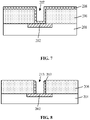
- a columnar structure 204 is formed on partial surface of the target layer 202.
- the columnar structure 204 determines a position and a shape of the subsequently formed annular pad.
- the columnar structure may be of a cylindrical shape or an elliptic cylindrical shape, or other suitable shapes (a cube shape or an oblong shape).
- a bottom area of the columnar structure 204 is smaller than an area of the target layer 202.
- a material of the columnar structure 204 may be different from materials of the target layer 202, the substrate 201 and the subsequently formed annular pad.
- the columnar structure 204 has a higher etch selectivity ratio than that for the target layer 202, the substrate 201 and the annular pad, and etching damage to the target layer 202, the substrate 201 and the annular pad is reduced or prevented.
- the columnar structure 204 may be made of a photoresist material or a mask material.
- the mask material may be one or more of silicon nitride, silicon oxide, silicon carbonitride, silicon oxynitride, polysilicon, amorphous silica, amorphous carbon and low-K dielectric material.
- the columnar structure 204 is made of the photoresist material, and the process of forming the columnar structure 204 includes the following steps.
- a photoresist layer is formed on the substrate 201 and the target layer 202.
- the photoresist layer is subjected to exposure and development to form the columnar structure on the target layer 202.
- the columnar structure 204 is made of the mask material, and the process of forming the columnar structure 204 includes the following steps.
- a mask material layer is formed on the substrate 201 and the target layer 202.
- the mask material layer is subjected to etching to form the columnar structure on the target layer 202.
- a pad material layer 205 is formed on a side wall and a top surface of the columnar structure 204, the substrate 201 and partial surface of the target layer 202.
- the pad material layer 205 is subsequently used for forming the annular pad.
- the pad material layer 205 is made of a material different from that of the subsequently formed dielectric layer.
- the dielectric layer In forming an etching hole in the dielectric layer subsequently, the dielectric layer has a higher etch selectivity ratio relative to that of the annular pad.
- the pad material layer 205 may be made of one or more of silicon nitride, silicon oxide, silicon carbonitride and silicon oxynitride.
- the pad material layer is formed by using a chemical vapor deposition process.
- a thickness of the pad material layer 205 determines a width of the subsequently formed annular pad and an enlarged size of a central via.
- the thickness of the pad material layer is 3 times or more of the size of the columnar structure or the subsequently formed central via.
- a size of a bottom of the central via may be efficiently enlarged in the subsequent process, so as to enable the central via to meet practical requirements.
- the pad material layer on the top surface of the columnar structure 204 as well as the substrate 201 and the partial surface of the target layer 202 is removed by etching without a mask, to form an annular pad 203 on a surface of the side wall of the columnar structure 204.
- the pad material layer is etched by an anisotropic dry etching process, which may be a plasma etching process.
- the size of the central via may be enlarged, so that the size of the bottom of the contact window structure may be enlarged; and in forming a metal plug in the contact window structure, a contact area between a bottom of the metal plug and the target layer may be increased, and a contact resistance between the bottom of the metal plug and the target layer is reduced. Furthermore, due to the existence of the annular pad, a depth or depth-to-width ratio of the etch hole formed in the dielectric layer may be reduced, so that the difficulty of forming hole etching is reduced.
- a size of a top of the formed contact window structure may be the same as or smaller than a size of a top formed according to the related technology, while the size of the bottom of the formed contact window structure is increased.
- a central via 213 is formed in the middle part of the annular pad 203, and partial surface of the target layer 202 is exposed from the central via 213.
- the columnar structure may be removed by wet etching or dry etching. In removing the columnar structure, an etch solution or etch gas with a higher etch selectivity ratio is used for the columnar structure relative to that for the annular pad 203, the target layer 202 and the substrate 201.
- FIG. 6 Another embodiment of the disclosure further provides a method of forming the annular pad 203.
- a mask material layer 206 is formed on the substrate 201 and partial surface of the target layer 202.
- a first via 207, from which the partial surface of the target layer is exposed, 202 is formed in the mask material layer 206.
- the mask material layer 206 may be made of one or more of photoresist, silicon nitride, silicon oxide, silicon carbonitride, silicon oxynitride, polysilicon, amorphous silica, amorphous carbon and low-K dielectric material.
- the mask material layer 206 may be formed by using the chemical vapor deposition process.
- the mask material layer 206 is made of a photoresist material
- the first via 207 is formed in the mask material layer 206 by exposure and developing processes.
- the first via 207 may be formed in the mask material layer 206 by an etching process.
- a shape and a position of the first via 207 determines a shape and a position of the subsequently formed annular pad.
- a pad material layer 208 is formed on a side wall and a bottom surface of the first via 207 as well as a surface of the mask material layer 206.
- the pad material layer 208 is subsequently used for forming the annular pad.
- the pad material layer 208 is made of a material different from that of a subsequently formed dielectric layer. In forming an etching hole in the dielectric layer subsequently, the dielectric layer has a higher etch selectivity ratio that that of the annular pad.
- the pad material layer 208 may be made of one or more of silicon nitride, silicon oxide, silicon carbonitride and silicon oxynitride.
- the pad material layer is formed by using the chemical vapor deposition process.
- a thickness of the pad material layer 208 determines a width of the subsequently formed annular pad and an enlarged size of a central through hole. In one embodiment, the thickness of the pad material layer 208 is 3 times or more of the size of the columnar structure or the subsequently formed central via.
- the pad material layer on the surface of the mask material layer 206 and the bottom surface of the first via is etched without a mask and removed to form the annular pad 203 on a surface of the side wall of the first via.
- the central via 213 is formed in the middle part of the annular pad 203.
- the pad material layer is etched by an anisotropic dry etching process, which may be a plasma etching process.
- the mask material layer 206 is removed after forming the annular pad 203.
- the mask material layer 206 may be removed by a wet etching process or a dry etching process.
- the mask material layer 206 is made of an isolation material and may be used for electrical isolation between devices, for example, when the mask material layer is made of a material the same as that of the subsequently formed dielectric layer, after the annular pad 203 is formed, the mask material layer 206 is retained, and the dielectric layer is directly formed on the mask material layer 206 subsequently, so that there is no need of an additional step to remove the mask material layer 206.
- FIG. 9 and FIG. 10 are top schematic diagrams of the structure of the foregoing formed annular pad 203.
- the annular pad 203 shown in FIG. 9 is of a circular ring shape, which facilitate the design of the contact window structure.
- the annular pad 203 shown in FIG. 10 is of an elliptic shape, which may reduce a resistance of a metal plug formed in the contact window structure subsequently. In other embodiments, the pad may of a strip shape, which may reduce the resistance of the metal plug formed in the contact window structure subsequently.
- FIG. 11 is carried out on the basis of FIG. 5 .
- a dielectric layer 211 is formed covering the substrate 201, the target layer 202 and the annular pad 203.
- the dielectric layer 211 is made of a material different from that of the annular pad 203.
- the dielectric layer 211 may be made of one of silicon nitride, silicon oxide, silicon carbonitride and silicon oxynitride.
- the dielectric layer 211 is formed by chemical vapor deposition.
- the dielectric layer 211 may be flatted by a flattening process, such that the dielectric layer 211 has a flat surface.
- the flattening process may be a chemical mechanical grinding process.
- the central via in the middle part of the annular pad 203 may be fully filled with the formed dielectric layer 211. In another embodiment, the central via may be partially filled or not filled with the dielectric layer 211.
- An air gap is formed in the annular pad. After the subsequent step of forming the etch hole in the dielectric layer, when continuing downward etching, it is very easy to expose the central via in the middle part of the annular pad 203 again, so as to prevent the influence on the size of the etch hole due to excessive long etching time.
- the air gap is formed by adjusting a step coverage rate of a depositing process during forming of the dielectric layer 211.
- the central via in the middle part of the annular pad 203 may be filled with a sacrificial layer.
- an etching rate of the sacrificial layer is greater than an etching rate of the dielectric layer, so that it is also very easy to expose the central via in the annular pad 203 again, so as to prevent the influence on the size of the etch hole due to excessive long etching time.
- the sacrificial layer may be made of a semiconductor insulation material such as silicon nitride, silicon oxynitride, silicon carbonitride or silicon oxycarbide. Referring to FIG. 12 , the dielectric layer 211 is etched, to form an etch hole 212 connected to the central via 213 in the dielectric layer 211.
- a patterned mask layer (for example, a patterned photoresist layer or a stack structure of patterned hard mask layers and photoresist layers) is formed on the dielectric layer 211.
- the patterned mask layer is used as a mask to etch the dielectric layer 211.
- a material for example, a dielectric layer material or a sacrificial layer material
- a material for example, a dielectric layer material or a sacrificial layer material
- the etch hole 212 formed in the dielectric layer 211 still has a high depth-to-width ratio, so that the size of the top of the formed etch hole 212 will be smaller than that of the bottom of the etch hole 212, that is, in a direction from an upper surface to a lower surface of the dielectric layer 211, the size of the etch hole 212 is gradually reduced.
- the size of the top of the etch hole and the size of the bottom of the etch hole may be the same.
- the dielectric layer 211 may be etched by an anisotropic dry etching process, such as an anisotropic plasma etching process.
- the dielectric layer 211 has a high etch selectivity ratio relative to the annular pad 203 (a specific etch selectivity ratio may be greater than or equal to 2:1).
- a bottom position of the etch hole 212 may be defined by the annular pad 203, and a diameter of the bottom of the etch hole 212 is smaller than an outer diameter of the annular pad 203.
- the annular pad 203 is removed along the etch hole 212 and the central via 213 (referring to FIG. 12 ) to enlarge the size of the central via 213, and the contact window structure is formed by the etch hole 212 and the central via 213 with the enlarged size.
- the annular pad may be removed by an isotropic wet or dry etching process.
- the annular pad 203 is removed by wet etching.
- An etching solution used for the wet etching is hot phosphoric acid.
- the size of the central via 213 is enlarged, such that a size 22 of the central via 213 will be greater than a size 23 of the bottom of the etch hole 212, that is, the size of the bottom of the formed contact window is increased relative to the size of the bottom of the contact window structure formed according to the related technology.
- a contact area between a bottom of the metal plug and the target layer may be increased, and a contact resistance between the bottom of the metal plug and the target layer is reduced.
- the target layer 202 is partially etched.
- the contact window structure is filled with metal to form a metal plug 214.
- the metal plug 214 is made of metal or other suitable conductive materials.
- a process of forming the metal plug 214 includes the following steps.
- a conductive material layer is formed on the contact window structure and a surface of the dielectric layer 211.
- the contact window structure is fully filled with the conductive material layer.
- the conductive material layer may be formed from metal (for example, tungsten) through a sputtering process.
- the conductive material layer higher than the surface of the dielectric layer 211 is removed by a chemical mechanical grinding process, and the metal plug 214 is formed in the contact window structure.
- a capacitor structure is formed in the contact window structure.
- the embodiments of the disclosure further provide a semiconductor structure.
- the semiconductor structure includes a target layer 202, an annular pad 203, a dielectric layer 211 and an etch hole 212.
- the annular pad 203 is located on a surface of the target layer 202, and a central via 213, from which partial surface of the target layer 202 is exposed, is formed in the middle part of the annular pad 203.
- the dielectric layer 211 covers the target layer 202 and the annular pad 203.
- the etch hole 212 is located in the dielectric layer 211 and is connected to the central via 213.
- the contact window structure includes a target layer 202, a dielectric layer 211 and a contact window structure.
- the dielectric layer 211 is located on the target layer 202.
- the contact window structure is located in the dielectric layer 211.
- the contact window structure includes an etch hole 212 and a central via 213 connected to each other.
- the etch hole 212 is located above the central via 213. Partial surface of the target layer is exposed from the central via 213.
- a size of the central via 213 is greater than that of a bottom of the etch hole 212.
- the metal plug includes a target layer 202, a dielectric layer 211, a contact window structure and a metal plug 214.
- the dielectric layer 211 is located on the target layer 202.
- the contact window structure is located in the dielectric layer 211.
- the contact window structure includes an etch hole 212 (referring to FIG. 13 ) and a central via 213 (referring to FIG. 13 ) connected to each other.
- the etch hole 212 is located above the central via 213. Partial surface of the target layer is exposed from the central via 213. A size of the central via 213 is greater than that of a bottom of the etch hole 212.
- the contact window structure is filled with the metal plug 214.
Landscapes
- Internal Circuitry In Semiconductor Integrated Circuit Devices (AREA)
Applications Claiming Priority (2)
| Application Number | Priority Date | Filing Date | Title |
|---|---|---|---|
| CN202011001855.8A CN114256136B (zh) | 2020-09-22 | 2020-09-22 | 接触窗结构、金属插塞及其形成方法、半导体结构 |
| PCT/CN2021/099873 WO2022062485A1 (zh) | 2020-09-22 | 2021-06-11 | 接触窗结构、金属插塞及其形成方法、半导体结构 |
Publications (3)
| Publication Number | Publication Date |
|---|---|
| EP4002437A4 EP4002437A4 (de) | 2022-05-25 |
| EP4002437A1 true EP4002437A1 (de) | 2022-05-25 |
| EP4002437B1 EP4002437B1 (de) | 2023-08-02 |
Family
ID=80740850
Family Applications (1)
| Application Number | Title | Priority Date | Filing Date |
|---|---|---|---|
| EP21773256.9A Active EP4002437B1 (de) | 2020-09-22 | 2021-06-11 | Verfahren zur herstellung einer kontaktöffnung |
Country Status (2)
| Country | Link |
|---|---|
| US (1) | US12002748B2 (de) |
| EP (1) | EP4002437B1 (de) |
Families Citing this family (3)
| Publication number | Priority date | Publication date | Assignee | Title |
|---|---|---|---|---|
| CN114256417A (zh) | 2020-09-22 | 2022-03-29 | 长鑫存储技术有限公司 | 电容结构及其形成方法 |
| CN114256135A (zh) * | 2020-09-22 | 2022-03-29 | 长鑫存储技术有限公司 | 开口结构及其形成方法、接触插塞及其形成方法 |
| CN119230482B (zh) * | 2024-12-04 | 2025-04-25 | 合肥晶合集成电路股份有限公司 | 半导体结构及其制备方法 |
Family Cites Families (37)
| Publication number | Priority date | Publication date | Assignee | Title |
|---|---|---|---|---|
| KR940000504B1 (ko) | 1991-03-20 | 1994-01-21 | 삼성전자 주식회사 | 반도체장치의 층간콘택구조 및 그 제조방법 |
| US5940731A (en) * | 1996-10-16 | 1999-08-17 | Vanguard International Semiconductor Corp. | Method for forming tapered polysilicon plug and plug formed |
| KR100265773B1 (ko) * | 1998-08-12 | 2000-09-15 | 윤종용 | 반도체장치의 접촉창의 제조방법 |
| US6136695A (en) | 1999-08-04 | 2000-10-24 | Taiwan Semiconductor Manufacturing Company | Method for fabricating a self-aligned contact |
| CN1204606C (zh) | 2001-12-04 | 2005-06-01 | 联华电子股份有限公司 | 形成具有高深宽比的沟槽的蚀刻方法 |
| KR100753122B1 (ko) | 2002-06-29 | 2007-08-29 | 주식회사 하이닉스반도체 | 반도체 장치의 캐패시터 제조방법 |
| KR20040017037A (ko) | 2002-08-20 | 2004-02-26 | 삼성전자주식회사 | 반도체 콘택 구조 및 그 형성 방법 |
| TWI223392B (en) | 2003-04-07 | 2004-11-01 | Nanya Technology Corp | Method of filling bit line contact via |
| KR100571673B1 (ko) | 2003-08-22 | 2006-04-17 | 동부아남반도체 주식회사 | 반도체 소자의 비아 홀 형성 방법 |
| KR20050066369A (ko) | 2003-12-26 | 2005-06-30 | 주식회사 하이닉스반도체 | 반도체 소자의 콘택홀 형성 방법 |
| CN100407419C (zh) | 2005-10-28 | 2008-07-30 | 联华电子股份有限公司 | 高深宽比开口及其制作方法 |
| KR20080093738A (ko) | 2007-04-18 | 2008-10-22 | 주식회사 하이닉스반도체 | 반도체 소자의 형성 방법 |
| US8008095B2 (en) * | 2007-10-03 | 2011-08-30 | International Business Machines Corporation | Methods for fabricating contacts to pillar structures in integrated circuits |
| US7829410B2 (en) | 2007-11-26 | 2010-11-09 | Micron Technology, Inc. | Methods of forming capacitors, and methods of forming DRAM arrays |
| JP5588123B2 (ja) | 2009-05-22 | 2014-09-10 | ピーエスフォー ルクスコ エスエイアールエル | 半導体装置及びその製造方法 |
| JP2011061067A (ja) | 2009-09-11 | 2011-03-24 | Elpida Memory Inc | 半導体装置の製造方法及び半導体装置 |
| US8357571B2 (en) * | 2010-09-10 | 2013-01-22 | Cree, Inc. | Methods of forming semiconductor contacts |
| JP5957840B2 (ja) | 2011-10-04 | 2016-07-27 | ソニー株式会社 | 半導体装置の製造方法 |
| CN103094186B (zh) | 2011-10-31 | 2015-04-01 | 中芯国际集成电路制造(上海)有限公司 | 半导体结构及其形成方法 |
| KR102057067B1 (ko) | 2013-01-29 | 2019-12-18 | 삼성전자주식회사 | 반도체 장치의 배선 구조체 및 그 형성 방법 |
| CN104347345B (zh) | 2013-07-24 | 2017-11-03 | 中芯国际集成电路制造(上海)有限公司 | 电容结构的形成方法 |
| US9076804B2 (en) | 2013-08-23 | 2015-07-07 | Taiwan Semiconductor Manufacturing Co., Ltd. | Systems and methods to enhance passivation integrity |
| CN104658962B (zh) | 2013-11-19 | 2017-09-22 | 中芯国际集成电路制造(上海)有限公司 | 通孔的形成方法 |
| US9230966B2 (en) | 2014-04-09 | 2016-01-05 | Nanya Technology Corp. | Capacitor and method of manufacturing the same |
| KR102424368B1 (ko) | 2015-10-15 | 2022-07-25 | 에스케이하이닉스 주식회사 | 반도체 장치 및 그 제조방법 |
| CN106611742B (zh) | 2015-10-26 | 2020-05-08 | 中芯国际集成电路制造(上海)有限公司 | 接触孔的形成方法 |
| US10381448B2 (en) * | 2016-05-26 | 2019-08-13 | Tokyo Electron Limited | Wrap-around contact integration scheme |
| US10217670B2 (en) * | 2016-09-07 | 2019-02-26 | Tokyo Electron Limited | Wrap-around contact integration scheme |
| JP2018049968A (ja) * | 2016-09-23 | 2018-03-29 | 東芝メモリ株式会社 | 集積回路装置及びその製造方法 |
| US10916499B2 (en) | 2016-09-30 | 2021-02-09 | Intel Corporation | Vias and gaps in semiconductor interconnects |
| US10037918B2 (en) | 2016-11-29 | 2018-07-31 | Taiwan Semiconductor Manufacturing Company, Ltd. | Contact structure and method of fabricating the same |
| KR102416028B1 (ko) * | 2017-04-07 | 2022-07-04 | 삼성전자주식회사 | 3차원 반도체 메모리 장치 및 그 제조 방법 |
| CN109037214B (zh) | 2017-06-12 | 2021-02-26 | 中芯国际集成电路制造(上海)有限公司 | 一种半导体器件及其制备方法和电子装置 |
| US10332787B2 (en) * | 2017-06-27 | 2019-06-25 | Taiwan Semiconductor Manufacturing Co., Ltd. | Formation method of interconnection structure of semiconductor device |
| US20200020711A1 (en) | 2018-07-13 | 2020-01-16 | Macronix International Co., Ltd. | Memory device and method of fabricating the same |
| US11276636B2 (en) * | 2019-07-31 | 2022-03-15 | International Business Machines Corporation | Adjustable via dimension and chamfer angle |
| CN211017076U (zh) | 2019-11-28 | 2020-07-14 | 长鑫存储技术有限公司 | 半导体结构 |
-
2021
- 2021-06-11 EP EP21773256.9A patent/EP4002437B1/de active Active
- 2021-08-13 US US17/401,461 patent/US12002748B2/en active Active
Also Published As
| Publication number | Publication date |
|---|---|
| US20220093509A1 (en) | 2022-03-24 |
| US12002748B2 (en) | 2024-06-04 |
| EP4002437A4 (de) | 2022-05-25 |
| EP4002437B1 (de) | 2023-08-02 |
Similar Documents
| Publication | Publication Date | Title |
|---|---|---|
| CN111199880B (zh) | 一种半导体器件的制造方法和半导体器件 | |
| KR20180120068A (ko) | 게이트 올 어라운드 반도체 장치 및 그 제조 방법 | |
| US12002748B2 (en) | Contact window structure, metal plug and forming method thereof, and semiconductor structure | |
| TW201913748A (zh) | 半導體裝置的形成方法 | |
| US11107726B2 (en) | Method for manufacturing bonding pad in semiconductor device | |
| CN107785426B (zh) | 一种半导体器件及其制造方法 | |
| CN112151608A (zh) | 半导体结构及其形成方法 | |
| US11615965B2 (en) | Semiconductor FinFET device and method | |
| US10998227B2 (en) | Metal insulator metal capacitor with extended capacitor plates | |
| US11769672B2 (en) | Semiconductor structure and forming method thereof | |
| US12532521B2 (en) | Method for manufacturing self-aligned exchange gates and associated semiconducting device | |
| WO2024026933A1 (zh) | 半导体结构及其形成方法 | |
| TW202322285A (zh) | 半導體結構及其形成方法 | |
| CN114256136B (zh) | 接触窗结构、金属插塞及其形成方法、半导体结构 | |
| TW201933612A (zh) | 接觸結構 | |
| US20250185356A1 (en) | Self-aligned backside gate cut dielectric with air gap | |
| US20230187216A1 (en) | Semiconductor FinFET Device and Method | |
| US20140120690A1 (en) | Streamlined Process for Vertical Semiconductor Devices | |
| US11929280B2 (en) | Contact window structure and method for forming contact window structure | |
| US20260082630A1 (en) | Self aligned backside channel removal | |
| TWI916840B (zh) | 積體電路裝置及其製作方法 | |
| US20260068222A1 (en) | Backside contact without rx liner | |
| CN110098174A (zh) | 帽结构 | |
| US20250176214A1 (en) | Backside dielectric liners | |
| US20230116155A1 (en) | Semiconductor structure and method for forming same |
Legal Events
| Date | Code | Title | Description |
|---|---|---|---|
| STAA | Information on the status of an ep patent application or granted ep patent |
Free format text: STATUS: UNKNOWN |
|
| STAA | Information on the status of an ep patent application or granted ep patent |
Free format text: STATUS: THE INTERNATIONAL PUBLICATION HAS BEEN MADE |
|
| PUAI | Public reference made under article 153(3) epc to a published international application that has entered the european phase |
Free format text: ORIGINAL CODE: 0009012 |
|
| STAA | Information on the status of an ep patent application or granted ep patent |
Free format text: STATUS: REQUEST FOR EXAMINATION WAS MADE |
|
| 17P | Request for examination filed |
Effective date: 20210929 |
|
| A4 | Supplementary search report drawn up and despatched |
Effective date: 20220412 |
|
| AK | Designated contracting states |
Kind code of ref document: A1 Designated state(s): AL AT BE BG CH CY CZ DE DK EE ES FI FR GB GR HR HU IE IS IT LI LT LU LV MC MK MT NL NO PL PT RO RS SE SI SK SM TR |
|
| RIN1 | Information on inventor provided before grant (corrected) |
Inventor name: YING, ZHAN Inventor name: WU, PING-HENG Inventor name: LIU, JIE |
|
| GRAP | Despatch of communication of intention to grant a patent |
Free format text: ORIGINAL CODE: EPIDOSNIGR1 |
|
| STAA | Information on the status of an ep patent application or granted ep patent |
Free format text: STATUS: GRANT OF PATENT IS INTENDED |
|
| DAV | Request for validation of the european patent (deleted) | ||
| DAX | Request for extension of the european patent (deleted) | ||
| INTG | Intention to grant announced |
Effective date: 20230309 |
|
| GRAS | Grant fee paid |
Free format text: ORIGINAL CODE: EPIDOSNIGR3 |
|
| GRAA | (expected) grant |
Free format text: ORIGINAL CODE: 0009210 |
|
| STAA | Information on the status of an ep patent application or granted ep patent |
Free format text: STATUS: THE PATENT HAS BEEN GRANTED |
|
| P01 | Opt-out of the competence of the unified patent court (upc) registered |
Effective date: 20230531 |
|
| AK | Designated contracting states |
Kind code of ref document: B1 Designated state(s): AL AT BE BG CH CY CZ DE DK EE ES FI FR GB GR HR HU IE IS IT LI LT LU LV MC MK MT NL NO PL PT RO RS SE SI SK SM TR |
|
| REG | Reference to a national code |
Ref country code: GB Ref legal event code: FG4D |
|
| REG | Reference to a national code |
Ref country code: CH Ref legal event code: EP |
|
| REG | Reference to a national code |
Ref country code: DE Ref legal event code: R096 Ref document number: 602021004016 Country of ref document: DE |
|
| REG | Reference to a national code |
Ref country code: IE Ref legal event code: FG4D |
|
| REG | Reference to a national code |
Ref country code: LT Ref legal event code: MG9D |
|
| REG | Reference to a national code |
Ref country code: NL Ref legal event code: MP Effective date: 20230802 |
|
| REG | Reference to a national code |
Ref country code: AT Ref legal event code: MK05 Ref document number: 1595787 Country of ref document: AT Kind code of ref document: T Effective date: 20230802 |
|
| PG25 | Lapsed in a contracting state [announced via postgrant information from national office to epo] |
Ref country code: GR Free format text: LAPSE BECAUSE OF FAILURE TO SUBMIT A TRANSLATION OF THE DESCRIPTION OR TO PAY THE FEE WITHIN THE PRESCRIBED TIME-LIMIT Effective date: 20231103 |
|
| PG25 | Lapsed in a contracting state [announced via postgrant information from national office to epo] |
Ref country code: IS Free format text: LAPSE BECAUSE OF FAILURE TO SUBMIT A TRANSLATION OF THE DESCRIPTION OR TO PAY THE FEE WITHIN THE PRESCRIBED TIME-LIMIT Effective date: 20231202 |
|
| PG25 | Lapsed in a contracting state [announced via postgrant information from national office to epo] |
Ref country code: SE Free format text: LAPSE BECAUSE OF FAILURE TO SUBMIT A TRANSLATION OF THE DESCRIPTION OR TO PAY THE FEE WITHIN THE PRESCRIBED TIME-LIMIT Effective date: 20230802 Ref country code: RS Free format text: LAPSE BECAUSE OF FAILURE TO SUBMIT A TRANSLATION OF THE DESCRIPTION OR TO PAY THE FEE WITHIN THE PRESCRIBED TIME-LIMIT Effective date: 20230802 Ref country code: PT Free format text: LAPSE BECAUSE OF FAILURE TO SUBMIT A TRANSLATION OF THE DESCRIPTION OR TO PAY THE FEE WITHIN THE PRESCRIBED TIME-LIMIT Effective date: 20231204 Ref country code: NO Free format text: LAPSE BECAUSE OF FAILURE TO SUBMIT A TRANSLATION OF THE DESCRIPTION OR TO PAY THE FEE WITHIN THE PRESCRIBED TIME-LIMIT Effective date: 20231102 Ref country code: NL Free format text: LAPSE BECAUSE OF FAILURE TO SUBMIT A TRANSLATION OF THE DESCRIPTION OR TO PAY THE FEE WITHIN THE PRESCRIBED TIME-LIMIT Effective date: 20230802 Ref country code: LV Free format text: LAPSE BECAUSE OF FAILURE TO SUBMIT A TRANSLATION OF THE DESCRIPTION OR TO PAY THE FEE WITHIN THE PRESCRIBED TIME-LIMIT Effective date: 20230802 Ref country code: LT Free format text: LAPSE BECAUSE OF FAILURE TO SUBMIT A TRANSLATION OF THE DESCRIPTION OR TO PAY THE FEE WITHIN THE PRESCRIBED TIME-LIMIT Effective date: 20230802 Ref country code: IS Free format text: LAPSE BECAUSE OF FAILURE TO SUBMIT A TRANSLATION OF THE DESCRIPTION OR TO PAY THE FEE WITHIN THE PRESCRIBED TIME-LIMIT Effective date: 20231202 Ref country code: HR Free format text: LAPSE BECAUSE OF FAILURE TO SUBMIT A TRANSLATION OF THE DESCRIPTION OR TO PAY THE FEE WITHIN THE PRESCRIBED TIME-LIMIT Effective date: 20230802 Ref country code: GR Free format text: LAPSE BECAUSE OF FAILURE TO SUBMIT A TRANSLATION OF THE DESCRIPTION OR TO PAY THE FEE WITHIN THE PRESCRIBED TIME-LIMIT Effective date: 20231103 Ref country code: FI Free format text: LAPSE BECAUSE OF FAILURE TO SUBMIT A TRANSLATION OF THE DESCRIPTION OR TO PAY THE FEE WITHIN THE PRESCRIBED TIME-LIMIT Effective date: 20230802 Ref country code: AT Free format text: LAPSE BECAUSE OF FAILURE TO SUBMIT A TRANSLATION OF THE DESCRIPTION OR TO PAY THE FEE WITHIN THE PRESCRIBED TIME-LIMIT Effective date: 20230802 |
|
| PG25 | Lapsed in a contracting state [announced via postgrant information from national office to epo] |
Ref country code: PL Free format text: LAPSE BECAUSE OF FAILURE TO SUBMIT A TRANSLATION OF THE DESCRIPTION OR TO PAY THE FEE WITHIN THE PRESCRIBED TIME-LIMIT Effective date: 20230802 |
|
| PG25 | Lapsed in a contracting state [announced via postgrant information from national office to epo] |
Ref country code: ES Free format text: LAPSE BECAUSE OF FAILURE TO SUBMIT A TRANSLATION OF THE DESCRIPTION OR TO PAY THE FEE WITHIN THE PRESCRIBED TIME-LIMIT Effective date: 20230802 |
|
| PG25 | Lapsed in a contracting state [announced via postgrant information from national office to epo] |
Ref country code: SM Free format text: LAPSE BECAUSE OF FAILURE TO SUBMIT A TRANSLATION OF THE DESCRIPTION OR TO PAY THE FEE WITHIN THE PRESCRIBED TIME-LIMIT Effective date: 20230802 Ref country code: RO Free format text: LAPSE BECAUSE OF FAILURE TO SUBMIT A TRANSLATION OF THE DESCRIPTION OR TO PAY THE FEE WITHIN THE PRESCRIBED TIME-LIMIT Effective date: 20230802 Ref country code: ES Free format text: LAPSE BECAUSE OF FAILURE TO SUBMIT A TRANSLATION OF THE DESCRIPTION OR TO PAY THE FEE WITHIN THE PRESCRIBED TIME-LIMIT Effective date: 20230802 Ref country code: EE Free format text: LAPSE BECAUSE OF FAILURE TO SUBMIT A TRANSLATION OF THE DESCRIPTION OR TO PAY THE FEE WITHIN THE PRESCRIBED TIME-LIMIT Effective date: 20230802 Ref country code: DK Free format text: LAPSE BECAUSE OF FAILURE TO SUBMIT A TRANSLATION OF THE DESCRIPTION OR TO PAY THE FEE WITHIN THE PRESCRIBED TIME-LIMIT Effective date: 20230802 Ref country code: CZ Free format text: LAPSE BECAUSE OF FAILURE TO SUBMIT A TRANSLATION OF THE DESCRIPTION OR TO PAY THE FEE WITHIN THE PRESCRIBED TIME-LIMIT Effective date: 20230802 Ref country code: SK Free format text: LAPSE BECAUSE OF FAILURE TO SUBMIT A TRANSLATION OF THE DESCRIPTION OR TO PAY THE FEE WITHIN THE PRESCRIBED TIME-LIMIT Effective date: 20230802 |
|
| REG | Reference to a national code |
Ref country code: DE Ref legal event code: R097 Ref document number: 602021004016 Country of ref document: DE |
|
| PG25 | Lapsed in a contracting state [announced via postgrant information from national office to epo] |
Ref country code: IT Free format text: LAPSE BECAUSE OF FAILURE TO SUBMIT A TRANSLATION OF THE DESCRIPTION OR TO PAY THE FEE WITHIN THE PRESCRIBED TIME-LIMIT Effective date: 20230802 |
|
| PLBE | No opposition filed within time limit |
Free format text: ORIGINAL CODE: 0009261 |
|
| STAA | Information on the status of an ep patent application or granted ep patent |
Free format text: STATUS: NO OPPOSITION FILED WITHIN TIME LIMIT |
|
| 26N | No opposition filed |
Effective date: 20240503 |
|
| PG25 | Lapsed in a contracting state [announced via postgrant information from national office to epo] |
Ref country code: SI Free format text: LAPSE BECAUSE OF FAILURE TO SUBMIT A TRANSLATION OF THE DESCRIPTION OR TO PAY THE FEE WITHIN THE PRESCRIBED TIME-LIMIT Effective date: 20230802 |
|
| PG25 | Lapsed in a contracting state [announced via postgrant information from national office to epo] |
Ref country code: BG Free format text: LAPSE BECAUSE OF FAILURE TO SUBMIT A TRANSLATION OF THE DESCRIPTION OR TO PAY THE FEE WITHIN THE PRESCRIBED TIME-LIMIT Effective date: 20230802 |
|
| PG25 | Lapsed in a contracting state [announced via postgrant information from national office to epo] |
Ref country code: BG Free format text: LAPSE BECAUSE OF FAILURE TO SUBMIT A TRANSLATION OF THE DESCRIPTION OR TO PAY THE FEE WITHIN THE PRESCRIBED TIME-LIMIT Effective date: 20230802 |
|
| PG25 | Lapsed in a contracting state [announced via postgrant information from national office to epo] |
Ref country code: MC Free format text: LAPSE BECAUSE OF FAILURE TO SUBMIT A TRANSLATION OF THE DESCRIPTION OR TO PAY THE FEE WITHIN THE PRESCRIBED TIME-LIMIT Effective date: 20230802 |
|
| REG | Reference to a national code |
Ref country code: CH Ref legal event code: PL |
|
| PG25 | Lapsed in a contracting state [announced via postgrant information from national office to epo] |
Ref country code: LU Free format text: LAPSE BECAUSE OF NON-PAYMENT OF DUE FEES Effective date: 20240611 |
|
| PG25 | Lapsed in a contracting state [announced via postgrant information from national office to epo] |
Ref country code: IE Free format text: LAPSE BECAUSE OF NON-PAYMENT OF DUE FEES Effective date: 20240611 |
|
| PG25 | Lapsed in a contracting state [announced via postgrant information from national office to epo] |
Ref country code: CH Free format text: LAPSE BECAUSE OF NON-PAYMENT OF DUE FEES Effective date: 20240630 Ref country code: BE Free format text: LAPSE BECAUSE OF NON-PAYMENT OF DUE FEES Effective date: 20240630 |
|
| REG | Reference to a national code |
Ref country code: BE Ref legal event code: MM Effective date: 20240630 |
|
| PGFP | Annual fee paid to national office [announced via postgrant information from national office to epo] |
Ref country code: DE Payment date: 20250618 Year of fee payment: 5 |
|
| PGFP | Annual fee paid to national office [announced via postgrant information from national office to epo] |
Ref country code: GB Payment date: 20250618 Year of fee payment: 5 |
|
| PGFP | Annual fee paid to national office [announced via postgrant information from national office to epo] |
Ref country code: FR Payment date: 20250627 Year of fee payment: 5 |
|
| PG25 | Lapsed in a contracting state [announced via postgrant information from national office to epo] |
Ref country code: CY Free format text: LAPSE BECAUSE OF FAILURE TO SUBMIT A TRANSLATION OF THE DESCRIPTION OR TO PAY THE FEE WITHIN THE PRESCRIBED TIME-LIMIT; INVALID AB INITIO Effective date: 20210611 |
|
| REG | Reference to a national code |
Ref country code: DE Ref legal event code: R079 Ref document number: 602021004016 Country of ref document: DE Free format text: PREVIOUS MAIN CLASS: H01L0021768000 Ipc: H10W0020000000 |
|
| PG25 | Lapsed in a contracting state [announced via postgrant information from national office to epo] |
Ref country code: HU Free format text: LAPSE BECAUSE OF FAILURE TO SUBMIT A TRANSLATION OF THE DESCRIPTION OR TO PAY THE FEE WITHIN THE PRESCRIBED TIME-LIMIT; INVALID AB INITIO Effective date: 20210611 |