EP3992704B1 - Liquid crystal element and illumination device - Google Patents
Liquid crystal element and illumination device Download PDFInfo
- Publication number
- EP3992704B1 EP3992704B1 EP20833071.2A EP20833071A EP3992704B1 EP 3992704 B1 EP3992704 B1 EP 3992704B1 EP 20833071 A EP20833071 A EP 20833071A EP 3992704 B1 EP3992704 B1 EP 3992704B1
- Authority
- EP
- European Patent Office
- Prior art keywords
- pixel electrode
- liquid crystal
- substrate
- pixel
- crystal element
- Prior art date
- Legal status (The legal status is an assumption and is not a legal conclusion. Google has not performed a legal analysis and makes no representation as to the accuracy of the status listed.)
- Active
Links
Images





Classifications
-
- G—PHYSICS
- G02—OPTICS
- G02F—OPTICAL DEVICES OR ARRANGEMENTS FOR THE CONTROL OF LIGHT BY MODIFICATION OF THE OPTICAL PROPERTIES OF THE MEDIA OF THE ELEMENTS INVOLVED THEREIN; NON-LINEAR OPTICS; FREQUENCY-CHANGING OF LIGHT; OPTICAL LOGIC ELEMENTS; OPTICAL ANALOGUE/DIGITAL CONVERTERS
- G02F1/00—Devices or arrangements for the control of the intensity, colour, phase, polarisation or direction of light arriving from an independent light source, e.g. switching, gating or modulating; Non-linear optics
- G02F1/01—Devices or arrangements for the control of the intensity, colour, phase, polarisation or direction of light arriving from an independent light source, e.g. switching, gating or modulating; Non-linear optics for the control of the intensity, phase, polarisation or colour
- G02F1/13—Devices or arrangements for the control of the intensity, colour, phase, polarisation or direction of light arriving from an independent light source, e.g. switching, gating or modulating; Non-linear optics for the control of the intensity, phase, polarisation or colour based on liquid crystals, e.g. single liquid crystal display cells
- G02F1/133—Constructional arrangements; Operation of liquid crystal cells; Circuit arrangements
- G02F1/1333—Constructional arrangements; Manufacturing methods
- G02F1/1343—Electrodes
- G02F1/134309—Electrodes characterised by their geometrical arrangement
-
- F—MECHANICAL ENGINEERING; LIGHTING; HEATING; WEAPONS; BLASTING
- F21—LIGHTING
- F21S—NON-PORTABLE LIGHTING DEVICES; SYSTEMS THEREOF; VEHICLE LIGHTING DEVICES SPECIALLY ADAPTED FOR VEHICLE EXTERIORS
- F21S41/00—Illuminating devices specially adapted for vehicle exteriors, e.g. headlamps
- F21S41/60—Illuminating devices specially adapted for vehicle exteriors, e.g. headlamps characterised by a variable light distribution
- F21S41/63—Illuminating devices specially adapted for vehicle exteriors, e.g. headlamps characterised by a variable light distribution by acting on refractors, filters or transparent cover plates
- F21S41/64—Illuminating devices specially adapted for vehicle exteriors, e.g. headlamps characterised by a variable light distribution by acting on refractors, filters or transparent cover plates by changing their light transmissivity, e.g. by liquid crystal or electrochromic devices
- F21S41/645—Illuminating devices specially adapted for vehicle exteriors, e.g. headlamps characterised by a variable light distribution by acting on refractors, filters or transparent cover plates by changing their light transmissivity, e.g. by liquid crystal or electrochromic devices by electro-optic means, e.g. liquid crystal or electrochromic devices
-
- G—PHYSICS
- G02—OPTICS
- G02F—OPTICAL DEVICES OR ARRANGEMENTS FOR THE CONTROL OF LIGHT BY MODIFICATION OF THE OPTICAL PROPERTIES OF THE MEDIA OF THE ELEMENTS INVOLVED THEREIN; NON-LINEAR OPTICS; FREQUENCY-CHANGING OF LIGHT; OPTICAL LOGIC ELEMENTS; OPTICAL ANALOGUE/DIGITAL CONVERTERS
- G02F2203/00—Function characteristic
- G02F2203/48—Variable attenuator
Definitions
- the present invention relates to a device (system) for irradiating light in a desired pattern in front of a vehicle, for example, and a liquid crystal element suitable for use in the device (system).
- JP 2005-183327 A discloses a vehicle headlight including at least a light emitting unit composed of at least one LED and an optical shielding unit which cuts off a part of the light irradiated toward the front from the light emitting unit and forms a cutoff suitable for the light distribution pattern of the vehicle headlight, where the optical shielding unit is comprised of an electro-optical element equipped with light control function and a control unit which controls lighting of the electro-optical element, and is configured to change shape of the light distribution pattern by selectively controlling the light control portion, by the electric switching control of the electro-optical element by the control unit.
- the electro-optical element a liquid crystal element is used, for example.
- the electro-optical element such as a liquid crystal element is configured to have a plurality of pixel electrodes in order to realize selective light control. These pixel electrodes are separated from each other so that a voltage can be applied individually, and a gap is provided between each of the pixels for electrical insulation. At this time, the gap between the pixel electrodes is, for example, about 10 ⁇ m depending on the formation accuracy. Further, when three or more rows of pixel electrodes are arranged, it is necessary to pass a wiring portion between the pixel electrodes for applying a voltage to each pixel, electrode in the intermediate row, thereby the gap between the pixel electrodes becomes larger.
- the gap between the pixel electrodes are portions that do not contribute to image formation, and cause dark lines to be generated in the light distribution pattern.
- an image formed by an electro-optical element an image corresponding to a light distribution pattern
- the above-described dark lines are also magnified and become easier to visually recognize, thereby, there is an inconvenience that the appearance of the light distribution pattern is worsened.
- narrowing the gap between the pixel electrodes can be considered as a solution, but in this case, since it causes an increase in manufacturing cost and may cause a problem such as a short circuit between the pixel electrodes, such a solution is not preferable.
- narrowing the width of the wiring portion to be disposed between the pixel electrodes can be considered as a solution, but in this case, since the resistance value of the wiring portion increases and it makes it difficult to apply necessary and sufficient voltage to the pixel electrodes, and since the probability of disconnection due to width narrowing also increases, such a solution is not preferable.
- inconveniences are not limited to a vehicle headlight, and the same can be said in a general lighting apparatus that controls the light distribution pattern using a liquid crystal element or the like.
- US 2009/059152 A1 was used as a basis for the preamble of claim 1 and discloses a liquid crystal display capable of narrowing a slit between pixel electrodes and preventing a short circuit defect.
- the liquid crystal display includes a plurality of pixels arranged in a matrix form, in which each of the pixels includes: a plurality of non-linear elements formed on a substrate; a plurality of subpixel electrodes electrically connected to the plurality of non-linear elements, respectively; and an inter-subpixel insulating layer formed between at least two subpixel electrode out of the plurality of subpixel electrodes.
- EP 3 401 591 A1 discloses a lamp unit used in a vehicular lamp system that selectively irradiates the front of a vehicle.
- the unit includes a light source, an optical shutter device, and an optical system where the optical shutter device has a first liquid crystal device having first light modulation areas and a second liquid crystal device having second light modulating areas.
- the first light modulation areas are arranged with a gap at least in a first direction and the second light modulation areas are arranged with a gap at least in the first direction.
- the first liquid crystal device and the second liquid crystal device overlap with each other such that, in a plan view, the first light modulation areas and the second light modulation areas are arranged complementarily to each other without forming a gap between the two modulation areas.
- a liquid crystal element is provided as set forth in claim 1.
- a lighting apparatus is provided as set forth in claim 4. Preferred embodiments of the present invention may be gathered from the dependent claims.
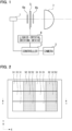
- FIG. 1 is a diagram showing the configuration of a vehicle headlight system of one embodiment.
- the vehicle headlight system shown in FIG. 1 is configured to include a light source 1, a camera 2, a controller 3, a liquid crystal driving device 4, a liquid crystal element 5, a pair of polarizers 6a and 6b, and a projection lens 7 .
- This vehicle headlight system detects the positions of a vehicle in front, pedestrians, etc. that exist around the own vehicle based on the images taken by the camera 2, sets a certain region including the position of the vehicle in front or the like as a non-irradiation region (dimming region), and sets the other region as the light irradiation region and performs selective light irradiation.
- the light source 1 is configured to include a white LED configured by combining a light emitting diode (LED) that emits blue light with a yellow phosphor, for example.
- the light source 1 is provided with a plurality of white LEDs arranged in a matrix or a line, for example.
- a laser, or a light source generally used for a vehicle headlight unit such as a light bulb or a discharge lamp can be used.
- the turn-on and turn-off state of the light source 1 is controlled by the controller 3.
- the light emitted from the light source 1 enters the liquid crystal element (liquid crystal panel) 5 via the polarizer 6a.
- another optical system for example, a lens, a reflecting mirror, or a combination thereof
- another optical system may exist on the path from the light source 1 to the liquid crystal element 5.
- the camera 2 captures the front of the own vehicle and outputs the image (information), and is arranged at a predetermined position (for example, the upper part inside the windshield) in the own vehicle.
- a predetermined position for example, the upper part inside the windshield
- the camera may be shared.
- the controller 3 detects the position of the vehicle in front or the like by performing image processing based on the image obtained by the camera 2 that captures the front of the own vehicle, sets a light distribution pattern in which the detected position of the vehicle in front or the like is set as the non-irradiation region and the other region is set as the light irradiation region, and generates a control signal for forming an image corresponding to this light distribution pattern to be supplied to the liquid crystal driving device 4.
- the controller 3 is realized by executing a predetermined operation program in a computer system having, for example, a CPU, a ROM, a RAM, or the like.
- the liquid crystal driving device 4 individually controls the alignment state of the liquid crystal layer in each pixel region of the liquid crystal element 5 by supplying a drive voltage to the liquid crystal element 5 based on a control signal supplied from the controller 3.
- the liquid crystal element 5 has, for example, a plurality of pixel regions (optical modulation regions) that can be individually controlled, and the transmittance of each pixel region is variably set according to the magnitude of the voltage applied to the liquid crystal layer provide by the liquid crystal driving device 4.
- the liquid crystal element 5 is provided with a vertically aligned liquid crystal layer, arranged between a pair of polarizers 6a and 6b in a crossed Nicol arrangement, the light transmittance becomes extremely low (light-shielding state) when no voltage (or a voltage below a threshold value) is applied to the liquid crystal layer, and the light transmittance becomes relatively high (transmission state) when a voltage is applied to the liquid crystal layer.
- the pair of polarizers 6a and 6b have their polarization axes substantially orthogonal to each other, for example, and are arranged so as to face each other with the liquid crystal element 5 interposed therebetween.
- a normally black mode which is an operation mode in which light is shielded (transmittance becomes extremely low) when no voltage is applied to the liquid crystal layer is assumed.
- an absorption type polarizer made of a general organic material iodine-based or dye-based
- a wire grid type polarizer is a polarizer formed by arranging ultrafine wires made of metal such as aluminum. Further, an absorption type polarizer and a wire grid type polarizer may be used in combination.
- the projection lens 7 spreads an image (an image having a contrast corresponding to the light irradiation region and the non-irradiation region) formed by the light transmitting through the liquid crystal element 5 in order to suit light distribution for headlights and projects it in front of the own vehicle, and an appropriately designed lens is used.
- an inverted projection type projector lens is used.
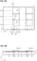
- FIG. 2 is a plan view for explaining the configuration of the liquid crystal element 5.
- FIG. 3 is a cross sectional view showing the configuration of the liquid crystal element 5.
- the cross sectional view shown in FIG. 3 corresponds to the cross section taken along the line a-a shown in FIG. 2 and FIG. 4 which is to be described later.
- the liquid crystal element 5 is configured to include a plurality of first pixel regions (first pixel portion) 51 and a plurality of second pixel regions (second pixel portion) 52.
- each second pixel region 52 is shown with a pattern so that each first pixel region 51 and each second pixel region 52 can be easily distinguished.
- the left-right direction of the liquid crystal element corresponds to the left-right direction of the light distribution projected in front of the own vehicle.
- Each first pixel region 51 and each second pixel region 52 are, for example, rectangular in a plan view as shown in FIG 2 . Further, each of the first pixel regions 51 and each of the second pixel regions 52 are connected to the liquid crystal driving device 4, and is statically driven, for example, and the light transmittance can be individually controlled. As shown in FIG. 3 , each first pixel region 51 applies a voltage to the liquid crystal layer 19 by each first pixel electrode (first individual electrode) 13 provided on a first substrate 11 side and a common electrode 18 provided on a second substrate 12 side, and by changing the alignment direction of the liquid crystal molecules in the liquid crystal layer 19 by the voltage, the transmittance of the light transmitting through each electrode is changed.
- Each second pixel region 52 applies a voltage to the liquid crystal layer 19 by each second pixel electrode (second individual electrode) 14 provided on the first substrate 11 side and a common electrode 18 provided on the second substrate 12 side, and by changing the alignment direction of the liquid crystal molecules in the liquid crystal layer 19 by the voltage, the transmittance of the light transmitting through each electrode is changed.
- each first pixel region 51 and each second pixel region 52 are arranged to have the ends of each region in contact with each other so that no gap is formed therebetween. Further, each first pixel region 51 and each second pixel region 52 are alternately arranged one by one along the X direction in the figure. Further, in the Y direction in the figure, each first pixel region 51 and each second pixel region 52 are arranged with a gap (for example, a few ⁇ m).
- the liquid crystal element 5 is configured to include a first substrate 11 and a second substrate 12 arranged to face each other, a plurality of first pixel electrodes 13 provided on the first substrate 11, a plurality of second pixel electrodes 14, an insulating film 15, a plurality of first wiring portions 21 and a plurality of second wiring portions 22, a common electrode 18 provided on the second substrate 12, and a liquid crystal layer 19 arranged between the first substrate 11 and the second substrate 12.
- the first substrate 11 and the second substrate 12 are appropriately provided with an alignment film in order to regulate the alignment state of the liquid crystal layer 19.
- the first substrate 11 and the second substrate 12 are each a rectangular substrate in a plan view, and are arranged so as to face each other.
- a transparent substrate such as a glass substrate or a plastic substrate can be used.
- a plurality of spherical spacers made of resin are dispersedly arranged between the first substrate 11 and the second substrate 12 for example, and the spacers keep the substrate gap at a desired distance (for example, approximately a few um) .
- columnar spacers made of resin may be used instead of the spherical spacers.
- Each first pixel electrode 13 is provided on one surface side of the first substrate 11. Further, each first wiring portion 21 is provided on one surface side of the first substrate 11. Further, each second wiring portion 22 is provided between each first pixel electrodes 13 on one surface side of the first substrate 11.
- Each first pixel electrode 13, each first wiring portion 21, and each second wiring portion 22 are configured by appropriately patterning a transparent conductive film such as indium tin oxide (ITO). The above-described first pixel region 51 is demarcated at each of the overlapping regions of the first pixel electrode 13 and the common electrode 18.
- Each second pixel electrode 14 is provided on the upper side of the insulating layer 15 on one surface side of the first substrate 11. That is, each first pixel electrode 13 is arranged closer to the first substrate 11 than each second pixel electrode 14.
- Each second pixel electrode 14 is configured by appropriately patterning a transparent conductive film such as indium tin oxide (ITO).
- ITO indium tin oxide
- Each first pixel electrode 13 and each second pixel electrode 14 are alternately arranged one by one in the X direction in the figure, and the ends of adjacent electrodes in the X direction are provided to slightly overlap each other in the Z direction in the figure.
- the overlapping region R which is the region where the ends of the adjacent first pixel electrodes 13 and the second pixel electrodes 14 partially overlap, has a width of approximately a few um to 15 um, for example.
- Each first wiring portion 21 is connected to one of the first pixel electrodes 13 to apply a voltage to the first pixel electrode 13 (refer to FIG. 4 to be described later).
- Each second wiring portion 22 is connected to one of the second pixel electrode 14 via the first insulating film 15 in order to apply a voltage to the second pixel electrode 14, and is arranged at a position where it overlaps with at least a part of one of the second pixel electrode 14 in a plan view.
- the insulating film 15 has translucency, and is provided on one surface side of the first substrate 11 so as to cover the upper side of each first pixel electrode 13.
- This insulating film 15 is, for example, an oxide film or a nitride film such as a SiO 2 film or a SiON film, and can be formed by a vapor phase process such as a sputtering method or a solution process.
- an organic insulating film may be used as the insulating film 15.
- the thickness of the insulating film 15 is preferably about 0.4 um to 1.5 um, for example.
- the dielectric constant of the insulating film 15 is preferred to be a high value, for example, 4 or more, and further preferably, 8 or more.
- the common electrode 18 is provided on one surface side of the second substrate 12. This common electrode 18 is provided so as to overlap all first pixel electrodes 13 and all second pixel electrodes 14 in a plan view.
- the common electrode 18 is configured by appropriately patterning a transparent conductive film such as indium tin oxide (ITO), for example.
- ITO indium tin oxide
- the liquid crystal layer 19 is interposed between the first substrate 11 and the second substrate 12.
- the liquid crystal layer 19 is configured by using a nematic liquid crystal material having a negative dielectric anisotropy ⁇ and having fluidity.
- the liquid crystal layer 19 of the present embodiment is set so that the alignment direction of the liquid crystal molecules when no voltage is applied is substantially vertically aligned.
- alignment films are provided on one surface side of the first substrate 11 and one surface side of the second substrate 12, respectively.
- a vertical alignment film that regulates the alignment state of the liquid crystal layer 19 to vertically align is used.
- Each alignment film is subjected to a uniaxial alignment treatment such as a rubbing treatment, and has a uniaxial alignment regulating force that regulates the alignment of the liquid crystal molecules of the liquid crystal layer 19 in that direction.
- the directions of the alignment treatment for each alignment film are set to be staggered (anti-parallel), for example.
- FIG. 4A is a plan view for explaining the configurations of the first pixel electrode, the first wiring portion, and the second wiring portion.
- FIG. 4B is a cross sectional view for explaining the configurations of the first pixel electrode, the first wiring portion, and the second wiring portion.
- each first pixel electrode 13 is provided in a region corresponding to each first pixel region 51.
- reference numerals 13a, 13b, and 13c are used in order to distinguish each of the first pixel electrodes 13.
- reference numerals 21a, 21b, and 21c are used in order to distinguish each of the first wiring portions 21, and reference numerals 22a, 22b, and 22c are used in order to distinguish each of the second wiring portions 22.
- a first pixel electrode 13a arranged in the lower part of the figure corresponds to one first pixel region 51.
- a first wiring portion 21a is connected to the first pixel electrode 13a.
- the first wiring portion 21a extends from the lower end of the first pixel electrode 13a to the lower end of the first substrate 11.
- a first pixel electrode 13b arranged in the middle part of the figure corresponds to one first pixel region 51.
- a first wiring portion 21b is connected to the first pixel electrode 13b.
- the first wiring portion 21b extends through the right side of each of the first pixel electrode 13b and the first pixel electrode 13a to the lower end of the first substrate 11.
- a first pixel electrode 13c arranged in the upper part of the figure corresponds to one first pixel region 51.
- a first wiring portion 21c is connected to the first pixel electrode 13c.
- the first wiring portion 21c extends through the right side of each of the first pixel electrode 13b, the first pixel electrode 13a, and the first wiring portion 21b, to the lower end of the first substrate 11.
- second wiring portions 22a, 22b, and 22c are arranged on the right side of the first pixel electrodes 13a, 13b, and 13c and the first wiring portions 21a, 21b, and 21c.
- the second wiring portion 22a is provided between the other second wiring portions 22b and 22c.
- the second wiring portion 22a is associated with a second pixel electrode 14a to be described later, and has a shorter length in the Y direction than the other second wiring portions 22b and 22c.
- the second wiring portion 22b is provided between the first wiring portion 21c and the second wiring portion 22a.
- the second wiring portion 22b is associated with a second pixel electrode 14b to be described later, and has a shorter length in the Y direction than the wiring portion 22c.
- the second wiring portion 22c is provided on the right side of the second wiring portion 22a.
- the second wiring portion 22c is associated with a second pixel electrode 14c to be described later, and has a longer length in the Y direction than the other wiring portions 22a and 22b.
- an inter-pixel electrode 23b extending in the X direction is connected to the second wiring portion 22b.
- the inter-pixel electrode 23b is provided so as to overlap with the gap (see FIG. 2 ) provided between adjacent second pixel regions 52 in the Y direction.
- an inter-pixel electrode 23c extending in the X direction is connected to the second wiring portion 22c. This inter-pixel electrode 23c is provided so as to overlap with the gap (see FIG. 2 ) provided between adjacent second pixel regions 52 in the Y direction.
- FIG. 5A is a plan view for explaining the configuration of the insulating film.
- FIG. 5B is a cross sectional view for explaining the configuration of the insulating film.
- the insulating film 15 is provided on one surface side of the first substrate 11 so as to cover each first pixel electrode 13, each first wiring portion 21, and each second wiring portion 22. Further, this insulating film 15 is provided with openings (through holes) 24a, 24b, and 24c for exposing a part of each of the second wiring portions 22a, 22b, and 22c. Through these openings 24a, 24b, and 24c, each of the second wiring portions 22a, 22b, and 22c and each of the second pixel electrodes 14a, 14b, and 14c (refer to FIG. 6A ) are physically and electrically connected to each other.
- FIG. 6A is a plan view for explaining the configuration of the second pixel electrode.
- FIG. 6B is a cross sectional view for explaining the configuration of the second pixel electrode.
- each second pixel electrode 14 is provided in a region corresponding to each second pixel region 52.
- reference numerals 14a, 14b, and 14c are used in order to distinguish each of the second pixel electrodes 14.
- a second pixel electrode 14a is physically and electrically connected to the second wiring portion 22a on the lower layer side via the opening 24a of the insulating film 15.
- a second pixel electrode 14b is physically and electrically connected to the second wiring portion 22b on the lower layer side via the opening 24b of the insulating film 15.
- a second pixel electrode 14c is physically and electrically connected to the second wiring portion 22c on the lower layer side via the opening 24c of the insulating film 15. Further, as described above, each of the second pixel electrodes 14a, 14b, and 14c is respectively arranged so as to have an overlapping region R between each of the first pixel electrodes 13a, 13b, and 13c.
- the second pixel electrodes 14a, 14b, and 14c are provided so as to overlap the first wiring portions 21b and 21c and the second wiring portions 22a, 22b, and 22c in a plan view. In this way, since the wiring portions can be arranged on the lower layer side of the pixel electrode, it is not necessary to secure a space for arranging the wiring portion outside each pixel region. Thereby, the gap between each pixel electrode can be eliminated.
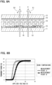
- FIG. 7 is a cross sectional view for explaining a state in which the first substrate and the second substrate are overlapped.
- a method for manufacturing the liquid crystal element of the present embodiment will be briefly described.
- each first pixel electrodes 13 and the like are formed on one surface side of the first substrate 11.
- the insulating film 15 is formed on one surface side of the first substrate 11 so as to cover each first pixel electrode 13 and the like, and the openings 24a, etc. are further formed.
- each second pixel electrode 14 is formed on the upper side of the insulating film 15.
- the common electrode 18 is formed on one surface side of the second substrate 12. Alignment treatment is appropriately performed to one surface side of each of the first substrate 11 and the second substrate 12 thus obtained, and both substrates are arranged to overlap each other. By injecting a liquid crystal material between the first substrate 11 and the second substrate 12, the liquid crystal layer 19 is formed. From the above, the liquid crystal element of the present embodiment can be obtained (refer to FIG. 3 ).
- the first wiring portion, the second wiring portion, and the common electrode of the liquid crystal element 5 are electrically connected to the liquid crystal driving device 4, and are configured so that the liquid crystal driving device 4 can supply a driving voltage to the liquid crystal element 5 based on a control signal supplied from the controller 3.
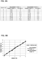
- FIG. 8A and FIG. 8B are diagrams for explaining the electro-optical characteristics (VT characteristics) of the first pixel region and the second pixel region.
- the measurement point which passes through the first pixel region 51 is defined as B
- the measurement point which passes through the second pixel region 52 is defined as A
- an example of measuring the electro-optical characteristics at each measurement point A and B at room temperature (25 °C) is shown in FIG. 8B .
- the voltage from the first pixel electrode 13 is divided by the insulating film 15 and then applied to the liquid crystal layer 19, whereas in the second pixel region 52, the voltage from the second pixel electrode 14 is directly applied to the liquid crystal layer 19.
- the voltage from the second pixel electrode 14 is directly applied to the liquid crystal layer 19.
- the voltage applied to the first pixel region 51 (measurement point B) is set to a value relatively larger than the voltage applied to the second pixel region 52 (measurement point A), in correspondence with the value equivalent to the voltage divided by the insulating film 15.
- C in and C LC can be expressed as follows.
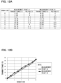
- FIG. 9A is a chart showing an example of setting the voltage applied to the first pixel electrode and the second pixel electrode at room temperature. Further, FIG. 9B is a graph showing the relationship between the transmittance and the gradation shown in FIG. 9A .
- a liquid crystal element in which the layer thickness of the liquid crystal layer 19 being 4 ⁇ m and the refractive index anisotropy ⁇ n being about 0.13 is used (the same applies hereinafter).
- the chart shows the applied voltage at which a desired transmittance can be obtained. It can be seen that the required voltages are different between measurement point A and measurement point B.
- the difference in transmittance at each of the measurement points A and B is within ⁇ 1.5%, and it can be said that the transmittances are substantially the same. Further, except for gradation "3", the difference in transmittance is within ⁇ 1.0%, and it can be said that the transmittances are substantially the same. In the case of forming high-intensity irradiation light in front of the vehicle as in the present embodiment, if the difference in transmittance is within ⁇ 2.0%, it can be said that the transmittances are substantially the same.
- FIG. 10A is a graph for explaining the electro-optical characteristics (VT characteristics) of the first pixel region and the second pixel region at an atmospheric temperature of 60 °C.
- FIG. 10B is a graph for explaining the electro-optical characteristics (VT characteristics) of the first pixel region and the second pixel region at an atmospheric temperature of 80 °C.
- VT characteristics electro-optical characteristics
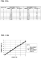
- FIG. 11A is a chart showing an example of setting the voltage applied to the first pixel electrode and the second pixel electrode at an atmospheric temperature of 60 °C. Further, FIG. 11B is a graph showing the relationship between the transmittance and the gradation shown in FIG. 11A .
- FIG. 12A is a chart showing an example of setting the voltage applied to the first pixel electrode and the second pixel electrode at an atmospheric temperature of 80 °C. Further, FIG. 12B is a graph showing the relationship between the transmittance and the gradation shown in FIG. 12A .
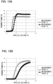
- FIG. 13A and FIG. 13B are graphs showing measurement examples of electro-optical characteristics with respect to obliquely incident light at room temperature.
- FIG. 13A shows the electro-optical characteristics when light is incident from 20 ° direction with respect to the substrate normal in a viewing direction
- FIG. 13B shows the electro-optical characteristics when light is incident from 20 ° direction with respect to the substrate normal in a reverse viewing direction.
- FIG. 14A is a chart showing the sum of the transmittances in the viewing direction and the reverse viewing direction of the voltage at each gradation shown in FIG. 9A described above.
- FIG. 14B is a graph showing the relationship between the transmittance and the gradation shown in FIG. 14A .
- the present invention is not limited to the contents of the above-described embodiment, and can be variously modified and implemented within the scope of the appended claims.
- vertical alignment is exemplified as the alignment mode of the liquid crystal layer of the liquid crystal element, but the alignment mode is not limited thereto, and for example, a twist alignment mode may be used.
- an optical compensator such as a C plate may be provided on one side or both sides of the liquid crystal element.
- a liquid crystal element where each of the pixel regions are arranged along the two directions which are the vertical direction and the lateral direction (X and Y directions) has been illustrated, but the liquid crystal element may be configured to have each pixel region arranged along at least one direction (for example, X direction).
Landscapes
- Physics & Mathematics (AREA)
- Chemical & Material Sciences (AREA)
- Crystallography & Structural Chemistry (AREA)
- Nonlinear Science (AREA)
- Geometry (AREA)
- Mathematical Physics (AREA)
- General Physics & Mathematics (AREA)
- Optics & Photonics (AREA)
- Engineering & Computer Science (AREA)
- General Engineering & Computer Science (AREA)
- Liquid Crystal (AREA)
- Devices For Indicating Variable Information By Combining Individual Elements (AREA)
Applications Claiming Priority (2)
| Application Number | Priority Date | Filing Date | Title |
|---|---|---|---|
| JP2019121990A JP7345293B2 (ja) | 2019-06-28 | 2019-06-28 | 液晶素子、照明装置 |
| PCT/JP2020/023374 WO2020262066A1 (ja) | 2019-06-28 | 2020-06-15 | 液晶素子、照明装置 |
Publications (3)
| Publication Number | Publication Date |
|---|---|
| EP3992704A1 EP3992704A1 (en) | 2022-05-04 |
| EP3992704A4 EP3992704A4 (en) | 2023-01-25 |
| EP3992704B1 true EP3992704B1 (en) | 2024-08-07 |
Family
ID=74061945
Family Applications (1)
| Application Number | Title | Priority Date | Filing Date |
|---|---|---|---|
| EP20833071.2A Active EP3992704B1 (en) | 2019-06-28 | 2020-06-15 | Liquid crystal element and illumination device |
Country Status (5)
| Country | Link |
|---|---|
| US (1) | US11906854B2 (https=) |
| EP (1) | EP3992704B1 (https=) |
| JP (1) | JP7345293B2 (https=) |
| CN (1) | CN114008522B (https=) |
| WO (1) | WO2020262066A1 (https=) |
Families Citing this family (2)
| Publication number | Priority date | Publication date | Assignee | Title |
|---|---|---|---|---|
| JP7730741B2 (ja) * | 2021-12-09 | 2025-08-28 | スタンレー電気株式会社 | 液晶装置、液晶装置の駆動方法 |
| WO2025182238A1 (ja) * | 2024-02-27 | 2025-09-04 | 株式会社ジャパンディスプレイ | 照明装置およびその駆動方法 |
Family Cites Families (13)
| Publication number | Priority date | Publication date | Assignee | Title |
|---|---|---|---|---|
| JP3326832B2 (ja) * | 1992-11-20 | 2002-09-24 | セイコーエプソン株式会社 | 液晶表示装置 |
| KR100260359B1 (ko) * | 1997-04-18 | 2000-07-01 | 김영환 | 액정 표시 장치 및 그 제조방법 |
| JP2005183327A (ja) | 2003-12-24 | 2005-07-07 | Stanley Electric Co Ltd | 車両前照灯 |
| EP2363744B1 (en) * | 2006-04-24 | 2015-12-16 | Sharp Kk | Liquid crystal display device |
| JP4407732B2 (ja) * | 2007-09-05 | 2010-02-03 | ソニー株式会社 | 液晶表示装置 |
| EP2230657B1 (en) * | 2008-01-10 | 2014-03-26 | Sharp Kabushiki Kaisha | Active matrix substrate and liquid crystal display device |
| JP2011027886A (ja) * | 2009-07-23 | 2011-02-10 | Seiko Epson Corp | 液晶装置の製造方法、液晶装置、電子機器 |
| WO2011096276A1 (en) | 2010-02-05 | 2011-08-11 | Semiconductor Energy Laboratory Co., Ltd. | Liquid crystal display device |
| JP2012113215A (ja) * | 2010-11-26 | 2012-06-14 | Stanley Electric Co Ltd | 液晶素子 |
| JP6808335B2 (ja) * | 2016-03-11 | 2021-01-06 | 株式会社ジャパンディスプレイ | 液晶表示装置 |
| CN106449652B (zh) | 2016-09-26 | 2019-05-28 | 京东方科技集团股份有限公司 | 阵列基板及其制造方法、显示面板和显示设备 |
| JP6869099B2 (ja) | 2017-05-11 | 2021-05-12 | スタンレー電気株式会社 | ランプユニット、車両用灯具システム |
| JP6941503B2 (ja) | 2017-08-24 | 2021-09-29 | スタンレー電気株式会社 | 車両用前照灯システム |
-
2019
- 2019-06-28 JP JP2019121990A patent/JP7345293B2/ja active Active
-
2020
- 2020-06-15 CN CN202080042906.3A patent/CN114008522B/zh active Active
- 2020-06-15 EP EP20833071.2A patent/EP3992704B1/en active Active
- 2020-06-15 WO PCT/JP2020/023374 patent/WO2020262066A1/ja not_active Ceased
- 2020-06-15 US US17/623,121 patent/US11906854B2/en active Active
Also Published As
| Publication number | Publication date |
|---|---|
| CN114008522B (zh) | 2024-03-12 |
| EP3992704A1 (en) | 2022-05-04 |
| CN114008522A (zh) | 2022-02-01 |
| WO2020262066A1 (ja) | 2020-12-30 |
| US20220229334A1 (en) | 2022-07-21 |
| JP2021009200A (ja) | 2021-01-28 |
| US11906854B2 (en) | 2024-02-20 |
| EP3992704A4 (en) | 2023-01-25 |
| JP7345293B2 (ja) | 2023-09-15 |
Similar Documents
| Publication | Publication Date | Title |
|---|---|---|
| US10830407B2 (en) | Vehicular lamp | |
| US10650765B2 (en) | Liquid crystal element and lighting apparatus | |
| EP3992704B1 (en) | Liquid crystal element and illumination device | |
| EP4032750B1 (en) | Vehicle lighting system | |
| US10781992B2 (en) | Vehicle headlamp system | |
| US11119365B2 (en) | Liquid crystal element, lighting apparatus | |
| JP2021173955A (ja) | 液晶素子、ランプユニット、車両用灯具システム | |
| JP7202934B2 (ja) | 液晶素子、照明装置 | |
| JP7369660B2 (ja) | ランプユニット、車両用灯具システム | |
| US20250027633A1 (en) | Liquid crystal element and lighting apparatus | |
| JP7197412B2 (ja) | 液晶素子、照明装置 | |
| JP2021046149A (ja) | 車両用灯具システム |
Legal Events
| Date | Code | Title | Description |
|---|---|---|---|
| STAA | Information on the status of an ep patent application or granted ep patent |
Free format text: STATUS: THE INTERNATIONAL PUBLICATION HAS BEEN MADE |
|
| PUAI | Public reference made under article 153(3) epc to a published international application that has entered the european phase |
Free format text: ORIGINAL CODE: 0009012 |
|
| STAA | Information on the status of an ep patent application or granted ep patent |
Free format text: STATUS: REQUEST FOR EXAMINATION WAS MADE |
|
| 17P | Request for examination filed |
Effective date: 20211220 |
|
| AK | Designated contracting states |
Kind code of ref document: A1 Designated state(s): AL AT BE BG CH CY CZ DE DK EE ES FI FR GB GR HR HU IE IS IT LI LT LU LV MC MK MT NL NO PL PT RO RS SE SI SK SM TR |
|
| DAV | Request for validation of the european patent (deleted) | ||
| DAX | Request for extension of the european patent (deleted) | ||
| A4 | Supplementary search report drawn up and despatched |
Effective date: 20221223 |
|
| RIC1 | Information provided on ipc code assigned before grant |
Ipc: F21S 41/64 20180101ALI20221219BHEP Ipc: G09F 9/30 20060101ALI20221219BHEP Ipc: G02F 1/133 20060101ALI20221219BHEP Ipc: G02F 1/13 20060101ALI20221219BHEP Ipc: G02F 1/1343 20060101AFI20221219BHEP |
|
| GRAP | Despatch of communication of intention to grant a patent |
Free format text: ORIGINAL CODE: EPIDOSNIGR1 |
|
| STAA | Information on the status of an ep patent application or granted ep patent |
Free format text: STATUS: GRANT OF PATENT IS INTENDED |
|
| RIC1 | Information provided on ipc code assigned before grant |
Ipc: F21S 41/64 20180101ALI20240213BHEP Ipc: G09F 9/30 20060101ALI20240213BHEP Ipc: G02F 1/133 20060101ALI20240213BHEP Ipc: G02F 1/13 20060101ALI20240213BHEP Ipc: G02F 1/1343 20060101AFI20240213BHEP |
|
| INTG | Intention to grant announced |
Effective date: 20240306 |
|
| GRAS | Grant fee paid |
Free format text: ORIGINAL CODE: EPIDOSNIGR3 |
|
| GRAA | (expected) grant |
Free format text: ORIGINAL CODE: 0009210 |
|
| STAA | Information on the status of an ep patent application or granted ep patent |
Free format text: STATUS: THE PATENT HAS BEEN GRANTED |
|
| AK | Designated contracting states |
Kind code of ref document: B1 Designated state(s): AL AT BE BG CH CY CZ DE DK EE ES FI FR GB GR HR HU IE IS IT LI LT LU LV MC MK MT NL NO PL PT RO RS SE SI SK SM TR |
|
| REG | Reference to a national code |
Ref country code: GB Ref legal event code: FG4D |
|
| REG | Reference to a national code |
Ref country code: CH Ref legal event code: EP |
|
| REG | Reference to a national code |
Ref country code: IE Ref legal event code: FG4D |
|
| REG | Reference to a national code |
Ref country code: DE Ref legal event code: R096 Ref document number: 602020035485 Country of ref document: DE |
|
| REG | Reference to a national code |
Ref country code: LT Ref legal event code: MG9D |
|
| REG | Reference to a national code |
Ref country code: NL Ref legal event code: MP Effective date: 20240807 |
|
| PG25 | Lapsed in a contracting state [announced via postgrant information from national office to epo] |
Ref country code: NO Free format text: LAPSE BECAUSE OF FAILURE TO SUBMIT A TRANSLATION OF THE DESCRIPTION OR TO PAY THE FEE WITHIN THE PRESCRIBED TIME-LIMIT Effective date: 20241107 |
|
| REG | Reference to a national code |
Ref country code: AT Ref legal event code: MK05 Ref document number: 1711601 Country of ref document: AT Kind code of ref document: T Effective date: 20240807 |
|
| PG25 | Lapsed in a contracting state [announced via postgrant information from national office to epo] |
Ref country code: NL Free format text: LAPSE BECAUSE OF FAILURE TO SUBMIT A TRANSLATION OF THE DESCRIPTION OR TO PAY THE FEE WITHIN THE PRESCRIBED TIME-LIMIT Effective date: 20240807 Ref country code: FI Free format text: LAPSE BECAUSE OF FAILURE TO SUBMIT A TRANSLATION OF THE DESCRIPTION OR TO PAY THE FEE WITHIN THE PRESCRIBED TIME-LIMIT Effective date: 20240807 Ref country code: GR Free format text: LAPSE BECAUSE OF FAILURE TO SUBMIT A TRANSLATION OF THE DESCRIPTION OR TO PAY THE FEE WITHIN THE PRESCRIBED TIME-LIMIT Effective date: 20241108 Ref country code: PT Free format text: LAPSE BECAUSE OF FAILURE TO SUBMIT A TRANSLATION OF THE DESCRIPTION OR TO PAY THE FEE WITHIN THE PRESCRIBED TIME-LIMIT Effective date: 20241209 Ref country code: PL Free format text: LAPSE BECAUSE OF FAILURE TO SUBMIT A TRANSLATION OF THE DESCRIPTION OR TO PAY THE FEE WITHIN THE PRESCRIBED TIME-LIMIT Effective date: 20240807 |
|
| PG25 | Lapsed in a contracting state [announced via postgrant information from national office to epo] |
Ref country code: BG Free format text: LAPSE BECAUSE OF FAILURE TO SUBMIT A TRANSLATION OF THE DESCRIPTION OR TO PAY THE FEE WITHIN THE PRESCRIBED TIME-LIMIT Effective date: 20240807 |
|
| PG25 | Lapsed in a contracting state [announced via postgrant information from national office to epo] |
Ref country code: LV Free format text: LAPSE BECAUSE OF FAILURE TO SUBMIT A TRANSLATION OF THE DESCRIPTION OR TO PAY THE FEE WITHIN THE PRESCRIBED TIME-LIMIT Effective date: 20240807 |
|
| PG25 | Lapsed in a contracting state [announced via postgrant information from national office to epo] |
Ref country code: AT Free format text: LAPSE BECAUSE OF FAILURE TO SUBMIT A TRANSLATION OF THE DESCRIPTION OR TO PAY THE FEE WITHIN THE PRESCRIBED TIME-LIMIT Effective date: 20240807 Ref country code: IS Free format text: LAPSE BECAUSE OF FAILURE TO SUBMIT A TRANSLATION OF THE DESCRIPTION OR TO PAY THE FEE WITHIN THE PRESCRIBED TIME-LIMIT Effective date: 20241207 |
|
| PG25 | Lapsed in a contracting state [announced via postgrant information from national office to epo] |
Ref country code: HR Free format text: LAPSE BECAUSE OF FAILURE TO SUBMIT A TRANSLATION OF THE DESCRIPTION OR TO PAY THE FEE WITHIN THE PRESCRIBED TIME-LIMIT Effective date: 20240807 |
|
| PG25 | Lapsed in a contracting state [announced via postgrant information from national office to epo] |
Ref country code: ES Free format text: LAPSE BECAUSE OF FAILURE TO SUBMIT A TRANSLATION OF THE DESCRIPTION OR TO PAY THE FEE WITHIN THE PRESCRIBED TIME-LIMIT Effective date: 20240807 Ref country code: RS Free format text: LAPSE BECAUSE OF FAILURE TO SUBMIT A TRANSLATION OF THE DESCRIPTION OR TO PAY THE FEE WITHIN THE PRESCRIBED TIME-LIMIT Effective date: 20241107 |
|
| PG25 | Lapsed in a contracting state [announced via postgrant information from national office to epo] |
Ref country code: RS Free format text: LAPSE BECAUSE OF FAILURE TO SUBMIT A TRANSLATION OF THE DESCRIPTION OR TO PAY THE FEE WITHIN THE PRESCRIBED TIME-LIMIT Effective date: 20241107 Ref country code: PT Free format text: LAPSE BECAUSE OF FAILURE TO SUBMIT A TRANSLATION OF THE DESCRIPTION OR TO PAY THE FEE WITHIN THE PRESCRIBED TIME-LIMIT Effective date: 20241209 Ref country code: PL Free format text: LAPSE BECAUSE OF FAILURE TO SUBMIT A TRANSLATION OF THE DESCRIPTION OR TO PAY THE FEE WITHIN THE PRESCRIBED TIME-LIMIT Effective date: 20240807 Ref country code: NO Free format text: LAPSE BECAUSE OF FAILURE TO SUBMIT A TRANSLATION OF THE DESCRIPTION OR TO PAY THE FEE WITHIN THE PRESCRIBED TIME-LIMIT Effective date: 20241107 Ref country code: NL Free format text: LAPSE BECAUSE OF FAILURE TO SUBMIT A TRANSLATION OF THE DESCRIPTION OR TO PAY THE FEE WITHIN THE PRESCRIBED TIME-LIMIT Effective date: 20240807 Ref country code: LV Free format text: LAPSE BECAUSE OF FAILURE TO SUBMIT A TRANSLATION OF THE DESCRIPTION OR TO PAY THE FEE WITHIN THE PRESCRIBED TIME-LIMIT Effective date: 20240807 Ref country code: IS Free format text: LAPSE BECAUSE OF FAILURE TO SUBMIT A TRANSLATION OF THE DESCRIPTION OR TO PAY THE FEE WITHIN THE PRESCRIBED TIME-LIMIT Effective date: 20241207 Ref country code: HR Free format text: LAPSE BECAUSE OF FAILURE TO SUBMIT A TRANSLATION OF THE DESCRIPTION OR TO PAY THE FEE WITHIN THE PRESCRIBED TIME-LIMIT Effective date: 20240807 Ref country code: GR Free format text: LAPSE BECAUSE OF FAILURE TO SUBMIT A TRANSLATION OF THE DESCRIPTION OR TO PAY THE FEE WITHIN THE PRESCRIBED TIME-LIMIT Effective date: 20241108 Ref country code: FI Free format text: LAPSE BECAUSE OF FAILURE TO SUBMIT A TRANSLATION OF THE DESCRIPTION OR TO PAY THE FEE WITHIN THE PRESCRIBED TIME-LIMIT Effective date: 20240807 Ref country code: ES Free format text: LAPSE BECAUSE OF FAILURE TO SUBMIT A TRANSLATION OF THE DESCRIPTION OR TO PAY THE FEE WITHIN THE PRESCRIBED TIME-LIMIT Effective date: 20240807 Ref country code: BG Free format text: LAPSE BECAUSE OF FAILURE TO SUBMIT A TRANSLATION OF THE DESCRIPTION OR TO PAY THE FEE WITHIN THE PRESCRIBED TIME-LIMIT Effective date: 20240807 Ref country code: AT Free format text: LAPSE BECAUSE OF FAILURE TO SUBMIT A TRANSLATION OF THE DESCRIPTION OR TO PAY THE FEE WITHIN THE PRESCRIBED TIME-LIMIT Effective date: 20240807 |
|
| PG25 | Lapsed in a contracting state [announced via postgrant information from national office to epo] |
Ref country code: SM Free format text: LAPSE BECAUSE OF FAILURE TO SUBMIT A TRANSLATION OF THE DESCRIPTION OR TO PAY THE FEE WITHIN THE PRESCRIBED TIME-LIMIT Effective date: 20240807 Ref country code: DK Free format text: LAPSE BECAUSE OF FAILURE TO SUBMIT A TRANSLATION OF THE DESCRIPTION OR TO PAY THE FEE WITHIN THE PRESCRIBED TIME-LIMIT Effective date: 20240807 |
|
| PG25 | Lapsed in a contracting state [announced via postgrant information from national office to epo] |
Ref country code: EE Free format text: LAPSE BECAUSE OF FAILURE TO SUBMIT A TRANSLATION OF THE DESCRIPTION OR TO PAY THE FEE WITHIN THE PRESCRIBED TIME-LIMIT Effective date: 20240807 |
|
| PG25 | Lapsed in a contracting state [announced via postgrant information from national office to epo] |
Ref country code: CZ Free format text: LAPSE BECAUSE OF FAILURE TO SUBMIT A TRANSLATION OF THE DESCRIPTION OR TO PAY THE FEE WITHIN THE PRESCRIBED TIME-LIMIT Effective date: 20240807 |
|
| PG25 | Lapsed in a contracting state [announced via postgrant information from national office to epo] |
Ref country code: SK Free format text: LAPSE BECAUSE OF FAILURE TO SUBMIT A TRANSLATION OF THE DESCRIPTION OR TO PAY THE FEE WITHIN THE PRESCRIBED TIME-LIMIT Effective date: 20240807 |
|
| REG | Reference to a national code |
Ref country code: DE Ref legal event code: R097 Ref document number: 602020035485 Country of ref document: DE |
|
| PLBE | No opposition filed within time limit |
Free format text: ORIGINAL CODE: 0009261 |
|
| STAA | Information on the status of an ep patent application or granted ep patent |
Free format text: STATUS: NO OPPOSITION FILED WITHIN TIME LIMIT |
|
| PGFP | Annual fee paid to national office [announced via postgrant information from national office to epo] |
Ref country code: DE Payment date: 20250625 Year of fee payment: 6 |
|
| PGFP | Annual fee paid to national office [announced via postgrant information from national office to epo] |
Ref country code: GB Payment date: 20250621 Year of fee payment: 6 |
|
| 26N | No opposition filed |
Effective date: 20250508 |
|
| PGFP | Annual fee paid to national office [announced via postgrant information from national office to epo] |
Ref country code: FR Payment date: 20250624 Year of fee payment: 6 |
|
| PG25 | Lapsed in a contracting state [announced via postgrant information from national office to epo] |
Ref country code: SE Free format text: LAPSE BECAUSE OF FAILURE TO SUBMIT A TRANSLATION OF THE DESCRIPTION OR TO PAY THE FEE WITHIN THE PRESCRIBED TIME-LIMIT Effective date: 20240807 |
|
| REG | Reference to a national code |
Ref country code: CH Ref legal event code: H13 Free format text: ST27 STATUS EVENT CODE: U-0-0-H10-H13 (AS PROVIDED BY THE NATIONAL OFFICE) Effective date: 20260127 |
|
| PG25 | Lapsed in a contracting state [announced via postgrant information from national office to epo] |
Ref country code: IT Free format text: LAPSE BECAUSE OF FAILURE TO SUBMIT A TRANSLATION OF THE DESCRIPTION OR TO PAY THE FEE WITHIN THE PRESCRIBED TIME-LIMIT Effective date: 20240807 |
|
| PG25 | Lapsed in a contracting state [announced via postgrant information from national office to epo] |
Ref country code: MC Free format text: LAPSE BECAUSE OF FAILURE TO SUBMIT A TRANSLATION OF THE DESCRIPTION OR TO PAY THE FEE WITHIN THE PRESCRIBED TIME-LIMIT Effective date: 20240807 |
|
| PG25 | Lapsed in a contracting state [announced via postgrant information from national office to epo] |
Ref country code: LU Free format text: LAPSE BECAUSE OF NON-PAYMENT OF DUE FEES Effective date: 20250615 |
|
| REG | Reference to a national code |
Ref country code: BE Ref legal event code: MM Effective date: 20250630 |
|
| PG25 | Lapsed in a contracting state [announced via postgrant information from national office to epo] |
Ref country code: IE Free format text: LAPSE BECAUSE OF NON-PAYMENT OF DUE FEES Effective date: 20250615 |
|
| PG25 | Lapsed in a contracting state [announced via postgrant information from national office to epo] |
Ref country code: RO Free format text: LAPSE BECAUSE OF FAILURE TO SUBMIT A TRANSLATION OF THE DESCRIPTION OR TO PAY THE FEE WITHIN THE PRESCRIBED TIME-LIMIT Effective date: 20240807 Ref country code: BE Free format text: LAPSE BECAUSE OF NON-PAYMENT OF DUE FEES Effective date: 20250630 |
|
| PG25 | Lapsed in a contracting state [announced via postgrant information from national office to epo] |
Ref country code: CH Free format text: LAPSE BECAUSE OF NON-PAYMENT OF DUE FEES Effective date: 20250630 |