EP3989445A1 - Untereinheit, mac-array, bit-breiten-rekonfigurierbares hybrides speicherinternes analog-digital-rechenmodul - Google Patents
Untereinheit, mac-array, bit-breiten-rekonfigurierbares hybrides speicherinternes analog-digital-rechenmodul Download PDFInfo
- Publication number
- EP3989445A1 EP3989445A1 EP21808967.0A EP21808967A EP3989445A1 EP 3989445 A1 EP3989445 A1 EP 3989445A1 EP 21808967 A EP21808967 A EP 21808967A EP 3989445 A1 EP3989445 A1 EP 3989445A1
- Authority
- EP
- European Patent Office
- Prior art keywords
- computing
- mac
- differential
- sub
- cells
- Prior art date
- Legal status (The legal status is an assumption and is not a legal conclusion. Google has not performed a legal analysis and makes no representation as to the accuracy of the status listed.)
- Withdrawn
Links
Images


Classifications
-
- H—ELECTRICITY
- H03—ELECTRONIC CIRCUITRY
- H03M—CODING; DECODING; CODE CONVERSION IN GENERAL
- H03M1/00—Analogue/digital conversion; Digital/analogue conversion
- H03M1/12—Analogue/digital converters
- H03M1/34—Analogue value compared with reference values
- H03M1/38—Analogue value compared with reference values sequentially only, e.g. successive approximation type
- H03M1/46—Analogue value compared with reference values sequentially only, e.g. successive approximation type with digital/analogue converter for supplying reference values to converter
- H03M1/466—Analogue value compared with reference values sequentially only, e.g. successive approximation type with digital/analogue converter for supplying reference values to converter using switched capacitors
- H03M1/468—Analogue value compared with reference values sequentially only, e.g. successive approximation type with digital/analogue converter for supplying reference values to converter using switched capacitors in which the input S/H circuit is merged with the feedback DAC array
-
- G—PHYSICS
- G11—INFORMATION STORAGE
- G11C—STATIC STORES
- G11C7/00—Arrangements for writing information into, or reading information out from, a digital store
- G11C7/10—Input/output [I/O] data interface arrangements, e.g. I/O data control circuits, I/O data buffers
- G11C7/1051—Data output circuits, e.g. read-out amplifiers, data output buffers, data output registers, data output level conversion circuits
- G11C7/1069—I/O lines read out arrangements
-
- G—PHYSICS
- G06—COMPUTING OR CALCULATING; COUNTING
- G06F—ELECTRIC DIGITAL DATA PROCESSING
- G06F7/00—Methods or arrangements for processing data by operating upon the order or content of the data handled
- G06F7/38—Methods or arrangements for performing computations using exclusively denominational number representation, e.g. using binary, ternary, decimal representation
- G06F7/48—Methods or arrangements for performing computations using exclusively denominational number representation, e.g. using binary, ternary, decimal representation using non-contact-making devices, e.g. tube, solid state device; using unspecified devices
- G06F7/544—Methods or arrangements for performing computations using exclusively denominational number representation, e.g. using binary, ternary, decimal representation using non-contact-making devices, e.g. tube, solid state device; using unspecified devices for evaluating functions by calculation
- G06F7/5443—Sum of products
-
- G—PHYSICS
- G06—COMPUTING OR CALCULATING; COUNTING
- G06N—COMPUTING ARRANGEMENTS BASED ON SPECIFIC COMPUTATIONAL MODELS
- G06N3/00—Computing arrangements based on biological models
- G06N3/02—Neural networks
- G06N3/04—Architecture, e.g. interconnection topology
-
- G—PHYSICS
- G06—COMPUTING OR CALCULATING; COUNTING
- G06N—COMPUTING ARRANGEMENTS BASED ON SPECIFIC COMPUTATIONAL MODELS
- G06N3/00—Computing arrangements based on biological models
- G06N3/02—Neural networks
- G06N3/04—Architecture, e.g. interconnection topology
- G06N3/0464—Convolutional networks [CNN, ConvNet]
-
- G—PHYSICS
- G06—COMPUTING OR CALCULATING; COUNTING
- G06N—COMPUTING ARRANGEMENTS BASED ON SPECIFIC COMPUTATIONAL MODELS
- G06N3/00—Computing arrangements based on biological models
- G06N3/02—Neural networks
- G06N3/06—Physical realisation, i.e. hardware implementation of neural networks, neurons or parts of neurons
- G06N3/063—Physical realisation, i.e. hardware implementation of neural networks, neurons or parts of neurons using electronic means
- G06N3/065—Analogue means
-
- G—PHYSICS
- G11—INFORMATION STORAGE
- G11C—STATIC STORES
- G11C11/00—Digital stores characterised by the use of particular electric or magnetic storage elements; Storage elements therefor
- G11C11/21—Digital stores characterised by the use of particular electric or magnetic storage elements; Storage elements therefor using electric elements
- G11C11/34—Digital stores characterised by the use of particular electric or magnetic storage elements; Storage elements therefor using electric elements using semiconductor devices
- G11C11/40—Digital stores characterised by the use of particular electric or magnetic storage elements; Storage elements therefor using electric elements using semiconductor devices using transistors
- G11C11/41—Digital stores characterised by the use of particular electric or magnetic storage elements; Storage elements therefor using electric elements using semiconductor devices using transistors forming static cells with positive feedback, i.e. cells not needing refreshing or charge regeneration, e.g. bistable multivibrator or Schmitt trigger
-
- G—PHYSICS
- G11—INFORMATION STORAGE
- G11C—STATIC STORES
- G11C11/00—Digital stores characterised by the use of particular electric or magnetic storage elements; Storage elements therefor
- G11C11/54—Digital stores characterised by the use of particular electric or magnetic storage elements; Storage elements therefor using elements simulating biological cells, e.g. neuron
-
- G—PHYSICS
- G11—INFORMATION STORAGE
- G11C—STATIC STORES
- G11C7/00—Arrangements for writing information into, or reading information out from, a digital store
- G11C7/10—Input/output [I/O] data interface arrangements, e.g. I/O data control circuits, I/O data buffers
- G11C7/1078—Data input circuits, e.g. write amplifiers, data input buffers, data input registers, data input level conversion circuits
- G11C7/109—Control signal input circuits
-
- G—PHYSICS
- G11—INFORMATION STORAGE
- G11C—STATIC STORES
- G11C7/00—Arrangements for writing information into, or reading information out from, a digital store
- G11C7/16—Storage of analogue signals in digital stores using an arrangement comprising analogue/digital [A/D] converters, digital memories and digital/analogue [D/A] converters
-
- H—ELECTRICITY
- H03—ELECTRONIC CIRCUITRY
- H03M—CODING; DECODING; CODE CONVERSION IN GENERAL
- H03M1/00—Analogue/digital conversion; Digital/analogue conversion
- H03M1/12—Analogue/digital converters
- H03M1/34—Analogue value compared with reference values
- H03M1/38—Analogue value compared with reference values sequentially only, e.g. successive approximation type
- H03M1/46—Analogue value compared with reference values sequentially only, e.g. successive approximation type with digital/analogue converter for supplying reference values to converter
- H03M1/462—Details of the control circuitry, e.g. of the successive approximation register
-
- Y—GENERAL TAGGING OF NEW TECHNOLOGICAL DEVELOPMENTS; GENERAL TAGGING OF CROSS-SECTIONAL TECHNOLOGIES SPANNING OVER SEVERAL SECTIONS OF THE IPC; TECHNICAL SUBJECTS COVERED BY FORMER USPC CROSS-REFERENCE ART COLLECTIONS [XRACs] AND DIGESTS
- Y02—TECHNOLOGIES OR APPLICATIONS FOR MITIGATION OR ADAPTATION AGAINST CLIMATE CHANGE
- Y02D—CLIMATE CHANGE MITIGATION TECHNOLOGIES IN INFORMATION AND COMMUNICATION TECHNOLOGIES [ICT], I.E. INFORMATION AND COMMUNICATION TECHNOLOGIES AIMING AT THE REDUCTION OF THEIR OWN ENERGY USE
- Y02D10/00—Energy efficient computing, e.g. low power processors, power management or thermal management
Definitions
- the present invention relates to the field of mixed-signal in-memory computing and, more specifically, to a sub-cell, a MAC array and a bit-width reconfigurable mixed-signal in-memory computing module.
- High energy efficiency means longer battery life
- high throughput per unit area means reduced area with a specified throughput, and in turn reduced cost.
- DNN deep neural networks
- MAC multiply-accumulate
- MAC implementation with traditional digital integrated circuits has a variety of advantages such as high tolerance to noise, high accuracy, good scalability and well-established design methodologies, but is not suitable to implement high energy-efficient large-scale neural networks due to the digital circuits' large chip areas and high power consumption.
- a 1-bit MAC operation consists of a multiplication portion equivalent to XNOR operations of 1-bit weights and a 1-bit input, whose results are stored in the form of voltages in capacitors, and an accumulation portion that obtains a result of the 1-bit MAC operation through equal sharing of a constant total amount of charge among the capacitors.
- Each 1-bit computing cell involved in this 1-bit MAC operation has 10 transistors.
- These conventional techniques described in Literatures 1 and 2 are associated with the following problems: (1) the transmission gate in each computing cell is unconditionally driven for every accumulation operation, disallowing the sparsity of input data to be utilized for power savings; (2) each 1-bit multiplication cell is separately equipped with an individual capacitor, and the metal-oxide-metal (MOM) capacitors of the successive approximation register (SAR) analog-to-digital converters (ADCs) are located outside of the computing static random access memory (SRAM) array because there is no space inside the array, which reduces the area efficiency; and (3) the accumulation operation through charge sharing requires connecting the top plates of the capacitors that store the XNOR operation results.
- MOM metal-oxide-metal
- This circuit topology makes the accumulation vulnerable to non-ideal effects like charge injection, clock feedthrough, nonlinear parasitic capacitance at the drains/sources of the transmission gate transistors, and leakage of the transistors connected to the capacitors' top plates, which result in computation errors. Further, the mismatch between the computing capacitors and digital-to-analog converter (DAC) capacitors in the ADCs resulted from physical layout mismatch can also result in computation errors.
- DAC digital-to-analog converter
- Conv-RAM an energy-efficient SRAM with embedded convolution computation for low-power CNN-based machine learning applications
- DOI 10.1109/ISSCC.2018.8310397
- an energy-efficient SRAM with embedded convolution computation there is provided an energy-efficient SRAM with embedded convolution computation.
- each 1-bit computing SRAM cell has 10 transistors, and the higher the number of transistors in each unit, the smaller the storage density; (2) it utilizes the parasitic capacitance on bit lines to store charge for the subsequent averaging operation, and the bit line parasitic capacitance is not well modeled and may suffer from larger mismatch compared to explicit capacitors like MOM capacitors, leading to inferior computation accuracy; (3) the horizontal charge averaging method used requires 6 extra transistors shared among several rows of cells, which limits the throughput because not all rows can perform the computation simultaneously; (4) the common-mode voltage on the differential charge averaging lines Vp AVG and Vn AVG is dependent on the magnitude of the input data X in and has been found to be inconstant as determined in an average value assessment using a local MAV circuit, so energy-efficient high-speed ADCs like SAR ADC cannot be easily used, and instead a ramp-based ADC that takes maximum 2 N -1 (N is the ADC resolution) steps to converge is used, which compromises the computation through
- each computing cell for 1-bit multiplication has too many transistors; there is one-to-one correspondence between capacitors storing the multiplication results to be accumulated and memory elements, i.e., the number of memory elements is equal to that of capacitors, but as one capacitor's area may be much larger than that of one SRAM cell, the capacitors can take up a significant proportion of the MAC array area, in particular when an advanced process is used; the transistors are unconditionally driven for every accumulation operation, leading to inferior energy efficiency; and a high rate of computation errors leads to a limited scope of application.
- an in-memory mixed-signal computing sub-cell for 1-bit multiplication comprising a conventional 6T SRAM cell, a complementary transmission gate, a first NMOS transistor and a computing capacitor,
- the filter parameter/weight w is written into and stored in the SRAM cell, and the input signal A is connected to the gate of the NMOS transistor in the complementary transmission gate. Additionally, the gate of the PMOS transistor in the complementary transmission gate is connected to the complementary input signal nA, and the gate of the first NMOS transistor is connected to the signal B. In particular, in this computing sub-cell, the complementary input signal nA is kept at the same voltage level as the signal B during computation. This topology can avoid unconditionally driving of the complementary transmission gate, resulting in improved energy efficiency.
- the branch of the computing capacitor connecting the first NMOS transistor is not conducting, while the branch of the computing capacitor connecting the complementary transmission gate is conducting.
- the multiplication result of the filter parameter w and the input signal A is stored as the bottom plate voltage V btm of the computing capacitor.
- the sub-cell for 1-bit multiplication (of the filter parameter w and the input signal A) has only 9 transistors and thus a reduced area.
- the complementary transmission gate is avoided from being connected to a top plate of the computing capacitor for charge accumulation.
- a plurality of such sub-cells may be arranged to form a computing cell in such a manner that the first NMOS transistor and the computing capacitor are shared among all the sub-cells in the computing cell.
- the sub-cells may be arranged in a feasible shape such as 2 ⁇ 2, 4 ⁇ 2, etc. Intuitively, this arrangement reduces the numbers of first NMOS transistors and computing capacitors used. For example, in a computing cell composed of 2 ⁇ 2 sub-cells, the number of the first NMOS transistors is reduced by 3 and the number of the computing capacitors is reduced by 3.
- the sub-cells in the computing cell may be activated in a time-multiplexed manner where, when one of the sub-cells is activated, all the other sub-cells are deactivated.
- another in-memory computation can be immediately initiated with a filter parameter stored in the SRAM cell of another sub-cell, without waiting for the transfer of data from outside into the SRAM. This results in significant enhancements in computation speed and throughput, and results in reductions in power consumption and area consumption.
- a MAC array for performing MAC operations, which comprises sub-cells according to the first aspect or possible implementations thereof.
- This MAC array includes a plurality of computing cells, and in each column of computing cells, the top plates of all the computing capacitors are connected to a respective accumulation bus.
- each computing cell in this design shares a common capacitor and a common transistor, allowing the MAC array to store more neural network parameters or activations for the next network layer.
- the results of 1-bit multiplication operations in the computing cells are stored in the computing capacitors, and the 1-bit multiplication results from the computing cells of each column in the MAC array are accumulated by the respective accumulation bus to which the top plates of the computing capacitors are connected, wherein a voltage on each accumulation bus corresponds to an accumulated sum of multiplication operation results of the respective column of the MAC array.
- the arrangement with multiple 1-bit multiplication sub-cells sharing a common transistor and a common computing capacitor for computation and storage can greatly improve the storage capacity per unit area.
- reducing data movement between inside and outside is the most important way to reduce power consumption.
- the MAC array of this design contains more SRAM cells per unit area, which can store more filter parameters of a neural network, reducing data movement.
- the MAC array may further include differential complementary transmission gates, differential computing capacitors and first PMOS transistors, wherein in each computing cell in the MAC array, the output of the CMOS inverter consisting of the MOS transistors M 3 , M 4 in each conventional 6T SRAM cell is connected to an input of a respective one of the differential complementary transmission gates, and all these differential complementary transmission gates connected to the respective CMOS inverters each consisting of the MOS transistors M 3 , M 4 are connected at their outputs to a drain of a respective one of the first PMOS transistors, the drain of the respective first PMOS transistor being in turn connected to a bottom plate of a respective one of the differential computing capacitors, the respective first PMOS transistor comprising a source connected to VDD.
- Differential multiplication results may be stored as bottom plate voltages of the respective differential computing capacitors, and top plates of the differential computing capacitors of the differential computing cells in each column may be connected to a respective differential accumulation bus.
- the MAC array may further comprise first CMOS inverters and differential computing capacitors, wherein in each of the computing cells in the MAC array, the outputs of all the complementary transmission gates are connected to an input of a respective one of the first CMOS inverters, which is in turn connected at an output thereof to a bottom plate of a respective one of the differential computing capacitors.
- Differential multiplication results may be stored as bottom plate voltages of the respective differential computing capacitors, and top plates of the differential computing capacitors in each column may be connected to a respective differential accumulation bus.
- a bit-width reconfigurable mixed-signal in-memory computing module comprising:
- the filter parameters or activations from computation in the neural network's previous layer are written into and stored in the MAC array via the filter/ifmap block following the conventional 6T SRAM write procedure so that logic 1 or 0 are stored in the SRAM of the sub-cells, and are subject to MAC operations with the input provided by the ifmap/filter block.
- the stored values in the sub-cells are multiplied with the input by digital operations that are equivalent to AND operations, and the multiplication results are stored in the computing capacitors.
- the accumulation portion as the top plates of the computing capacitors in each column are connected together by a respective accumulation bus, charge stored in the computing capacitors is shared via the accumulation bus.
- the column-wise accumulation results are represented in the form of analog voltages, which are then converted into their digital representations by the ADC block.
- the digital representations are processed, and the final output results are partial sums or activations usable as an input to the next network layer.
- much power is consumed in MAC operations.
- the mixed-signal MAC operations can greatly reduce power consumption, and the reduced area implementation of the MAC array can result in improved energy efficiency and a faster computation speed.
- Using different combinations of operations in different phases of computation in neural networks allows different benefits of analog and digital operations to be effectively taken advantage of to ensure low computational power consumption, high energy efficiency, a high speed and high accuracy.
- the ADC block may be implemented as SAR ADCs, in particular binarily weighted capacitive SAR ADCs.
- the sparsity of the MAC array's input and stored values may spare some capacitors in the SAR DACs from switching in order to achieve higher energy efficiency and faster analog-to-digital conversion.
- a bit-width of the SAR ADC for each column in the MAC array may be determined in real time by the sparsity of the input and stored values.
- each SAR DAC may be connected together with a MAC DAC.
- the MAC DAC is a respective column of computing capacitors in the MAC array.
- the capacitors in the column of the MAC array may be connected in parallel with capacitors in the SAR DAC.
- the reuse of the MAC DAC as the SAR DAC is allowed via bottom-plate sampling.
- both MAC operation and analog-to-digital conversion can be accomplished with a single capacitor array, avoiding mismatch and accuracy loss caused by the use of separate capacitor arrays for the MAC DAC for performing MAC operations and the SAR DAC for achieving analog-to-digital conversion, allowing the possibility of fully-differential SAR ADC, and better solving the problem of common-mode dependent comparator input offset voltage.
- bit-width reconfigurable mixed-signal computing modules provided in embodiments of the present invention can be used in visual and acoustic DNN architectures, in particular in object detection, acoustic feature extraction with low power consumption, etc.
- a feature extractor convolves data to be processed with a filter consisting of weights and outputs feature maps. Depending on the filter selected, different features may be extracted.
- the convolution operation of the data to be processed with the filter is most power-consuming, necessitating the avoidance of power consumption in unconditional circuit driving or the like, in particular when the data to be processed is a sparse matrix.
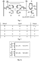
- Fig. 1 is a structural schematic of a sub-cell for 1-bit multiplication according to an embodiment of the present invention, which includes a conventional 6T SRAM cell, a complementary transmission gate, a first NMOS transistor and a computing capacitor.
- the conventional 6T SRAM cell consists of MOS transistors M 1 , M 2 , M 3 , M 4 , M 5 , M 6 .
- a CMOS inverter consisting of the MOS transistors M 1 , M 2 is cross-coupled to a CMOS inverter consisting of the MOS transistors M 3 , M 4 .
- the cross-coupled two CMOS inverters store a 1-bit filter parameter, and the MOS transistors M 5 , M 6 act as control switches for bit lines for reading and writing the filter parameter.
- An output of the CMOS inverter consisting of the MOS transistors M 1 , M 2 in the conventional 6T SRAM cell is connected to an input of the complementary transmission gate, and an output of the complementary transmission gate is connected to a drain of the first NMOS transistor.
- a source of the first NMOS transistor is grounded, and the drain thereof is connected to a bottom plate of the computing capacitor.
- a gate of an NMOS transistor is connected to an input signal and a gate of a PMOS transistor is at the same voltage level as a signal input to a gate of the first NMOS transistor.
- a multiplication result of the input signal and the filter parameter is stored as a voltage on the bottom plate of the computing capacitor, and a plurality of such computing sub-cells are arranged to form a computing cell in such a manner that the first NMOS transistor and the computing capacitor are shared among all the sub-cells in the computing cell.
- the input signals at the NMOS and PMOS gates of the complementary transmission gate are denoted at A and nA, and the signal at the gate of the first NMOS transistor are denoted at B.
- the signals B and nA may be the same.
- the signals B and nA may be at the same voltage level by connecting both to a common node.
- the conventional 6T SRAM stores the filter parameter W that is written therein following the conventional 6T SRAM write procedure, in which a word line WL is set to VDD and bit lines BL, nBL to 0 or 1 depending on the value to be written.
- the word line WL is set at a high voltage level to VDD, and the MOS transistors M 5 and M 6 are both conducting.
- the bit line BL is set to 0 and nBL to VDD.
- the sub-cell may follow the procedure below to perform a 1-bit multiplication operation:
- the sub-cell accomplishes the 1-bit multiplication operation (of the filter parameter w and the input signal A) with only 9 transistors, thus having a reduced sub-cell area and higher energy efficiency.
- the first NMOS transistor is included in the sub-cell for the purpose of control, and the 1-bit multiplication operation result of the input signal A and the filter parameter w stored in the SRAM cell is stored as the bottom plate voltage of the computing capacitor.
- the structure in which the SRAM cell is connected to the complementary transmission gate and contains 8 transistors is referred to as an 8T structure (or 8T sub-cell, as it contains eight transistors).
- This computing sub-cell is an extended version of the conventional 6T SRAM cell.
- a plurality of the sub-cells may be arranged in a feasible shape such as 2 ⁇ 2, 4 ⁇ 2, etc., as shown in Fig. 3a , to form a computing cell.
- Fig. 3b shows such a computing cell composed of four sub-cells.
- WL 0 denotes a word line common to the sub-cells a and b; WL 1 , a word line common to the sub-cells c and d; BL 0 and nBL 0 , bit lines common to the sub-cells a and c; BL 1 and nBLi, bit lines common to the sub-cells b and d; Bo, the gate signal; W 0a -W 0d and nW 0a -nW 0d , weight storage locations in the four sub-cells; and V btm0 ; the bottom plate voltage of the first computing cell.
- each sub-cell retains its own 8T (sub-cell) structure, and all the sub-cells share a common first NMOS transistor and a common computing capacitor.
- the output of the complementary transmission gate in each sub-cell is connected to the drain of the common first NMOS transistor, which is in turn connected to the bottom plate of the common computing capacitor. That is, every such computing cell contains only one first NMOS transistor and one computing capacitor, which are shared by all the sub-cells contained in the computing cell to perform 1-bit multiplication operations. Intuitively, this arrangement reduces the numbers of necessary first NMOS transistors and computing capacitors.
- the number of the first NMOS transistors is reduced by 3 and the number of the computing capacitors is reduced by 3. It can be understood that the more sub-cells share one first NMOS transistor and one computing capacitor, the closer the average number of transistors in each sub-cells is to 8.
- the arrangement with multiple 1-bit multiplication sub-cells sharing a single capacitor can greatly improve the storage capacity per unit area. That is, more filter parameters or weights can be stored per area, compared to the conventional techniques.
- the sub-cells in the computing cell may be activated in a time-multiplexed manner. That is, when any sub-cell is activated, all the other sub-cells are deactivated.
- the activated sub-cell can perform a 1-bit multiplication operation in the way as described above according to the truth table in Fig. 3c .
- the input signal B i at the first NMOS transistor's gate is controlled separately from the input signal nAij at the PMOS gate of the complementary transmission gate in each sub-cell.
- the complementary input signal nAij in the activated sub-cell at a given time remains at the same voltage level as the signal B i , this is no longer realized by connection at a common node.
- sharing of a computing capacitor and a first NMOS transistor among sub-cells means that the computing cell includes multiple sub-cells capable of multiplication and accumulation.
- the computing cell saves the use of n-1 computing capacitors and n-1 first NMOS transistors, making the number of transistors required for each sub-cell to perform a 1-bit multiplication operation closer to 8. Due to being fabricated by different processes, the area of the computing capacitor is typically several times that of a SRAM cell. By reducing the number of computing capacitors per unit area, the sharing arrangement can impart higher storage capacity to an array module made up of those computing cells.
- a multiply-accumulate (MAC) array for MAC operation is provided on the basis of the sub-cells according to the first aspect and possible implementations thereof.
- the MAC array includes a plurality of the computing cells, and in each column of computing cells, the top plates of the computing capacitors are connected to a respective accumulation bus.
- the computing cells with shared capacitors and transistors enable the MAC array to store more neural network parameters or computation results from the previous network layer. Specifically, the results of 1-bit multiplication operations in the computing cells are stored in the computing capacitors, and the 1-bit multiplication results from the computing cells of each column in the MAC array are accumulated by the respective accumulation bus to which the top plates of the computing capacitors are connected.
- V top the voltage on the accumulation bus is V top .
- the plurality of computing cells are column-wise arranged so that each computing cell corresponds to one computing capacitor and contains a plurality of sub-cells according to the first aspect or embodiments thereof.
- V btm0 -V btm(N-1) denote the bottom plate voltages of the first through N-th computing cells.
- the MAC array may follow "Procedure I" below to perform a MAC operation:
- the MAC array may follow "Procedure II" below to perform an operation:
- the MAC array may be in particular used in computation with multi-bit weights.
- each column of computing cells performs a bit-wise MAC operation, and the multi-bit computation results can be obtained by performing shift-add operations on digital representations resulting from analog-to-digital conversion.
- each column may perform a bit-wise MAC operation, e.g., the first column for the least significant bit (LSB) (i.e., performing a MAC operation between the 0-th bit values and the input signals) and the k-th column for the most significant bit (MSB) (i.e., performing a MAC operation between the k-th bit values and the input signals).
- LSB least significant bit
- MSB most significant bit
- each column separately performs an MAC operation for one bit of multi-bit binary weights, and the MAC results of all the involved columns contain k elements, which are then subject to analog-to-digital conversion and shift-add operations in the digital domain.
- the MAC array further includes differential complementary transmission gates, differential computing capacitors and first PMOS transistors.
- the output of the CMOS inverter consisting of the MOS transistors M 3 , M 4 in each conventional 6T SRAM cell is connected to an input of a respective one of the differential complementary transmission gates, and all these differential complementary transmission gates connected to the respective CMOS inverters each consisting of the MOS transistors M 3 , M 4 are connected at their outputs to a drain of a respective one of the first PMOS transistors.
- the drain of the respective first PMOS transistor is in turn connected to a bottom plate of a respective one of the differential computing capacitors, and a source thereof is connected to VDD.
- Differential multiplication results are stored as bottom plate voltages of the respective differential computing capacitors, and top plates of the differential computing capacitors of the differential computing cells in each column are connected to a respective differential accumulation bus.
- a 10T structure or 10T sub-cell, as it contains ten transistors.
- the computing cells connected in the MAC array in Fig. 5b are referred to as first differential cells.
- each first differential cell can be considered as an extension of the above-described computing cells, and hence of the sub-cells constituting the computing cells.
- each first differential cell further includes some commonly shared transistors and capacitors, more specifically, a common first NMOS transistor, a common first PMOS transistor, a common differential computing capacitor and a common computing capacitor.
- the sub-cells in each first differential cell may be activated in a similar time-multiplexed manner.
- the MAC array may further include first CMOS inverters and differential computing capacitors.
- the outputs of all the complementary transmission gates are connected to an input of a respective one of the first CMOS inverter, and an output of the respective first CMOS inverter is connected to a bottom plate of a respective one of the differential computing capacitors.
- the structure in which the 6T SRAM cell is connected to the complementary transmission gate is referred to as an 8T structure (or 8T sub-cell, as it contains eight transistors). Accordingly, the computing cells connected in the MAC array in Fig.
- each second differential cell 6b are referred to as second differential cells, in which differential multiplication results are stored as bottom plate voltages of the differential computing capacitors.
- each second differential cell further includes some commonly shared transistors and capacitors, more specifically, a common first NMOS transistor, a common first CMOS inverter, a common differential computing capacitor and a common computing capacitor. Further, the sub-cells in each second differential cell may be activated in a similar time-multiplexed manner.
- Fig. 6c is a schematic diagram of a differential MAC array architecture made up of the above-described first or second differential cells, in which in each column, the top plates of all the computing capacitors are connected to a respective accumulation bus, and the top plates of all the differential computing capacitors are connected to a respective differential accumulation bus.
- V top_p_1 , V top_p_2 , V top_n_1 and V top_n_2 denote voltages resulting from computation in the differential computing cells.
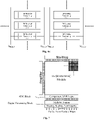
- a bit-width reconfigurable mixed-signal computing module includes: the MAC array according to the second aspect or any possible implementation thereof, wherein column-wise accumulation results are represented in the form of analog voltages, i.e., the top plate voltages V top of the capacitors described in connection with the above embodiments; a filter/ifmap block for providing filter parameters (or computation results from the previous network layer in the case of a neural network, as will be appreciated) that are written into and stored in the MAC array; an ifmap/filter block for providing an input to the MAC array, more specifically, to the complementary transmission gates in the computing cells, which is subject to MAC operations with the filter parameters or the activations from the previous network layer; an ADC block for converting the analog voltages resulting from the MAC operations to their digital representations; and a digital processing block for performing at least multi-bit fusion, biasing, scaling or nonlinearity on the digital representations output from the ADC block and for out
- the module described herein when used in a neural network to perform MAC operations, may be typically able to pre-load the necessary filter parameters (weights) at once because it contains more memory elements (i.e., 6T SRAM cells) per unit area.
- the output partial sums or final activations (feature maps) directly usable in computation in the next network layer can be immediately subject to MAC operations with the filter parameters (weights) pre-loaded and stored in the module, saving the time waiting for off-chip data movement and the power consumed therein as well.
- the high throughput of the module can improve on-chip storage capabilities.
- the memory cells in the MAC array can also be used to store the output activations (feature maps) of the same network layer.
- the computing cells also share some transistors and other devices involved in the analog-to-digital conversion and digital processing in other regions of the module than the MAC array.
- the ADC block may be parallel capacitive SAR ADCs for converting the top plate voltages Vtop column-wise output from the computing cells to their digital representations.
- Each of the SAR ADCs may include a MAC DAC, a SAR DAC, a comparator, a switching sequence and SAR logic for controlling the switching sequence.
- the parallel capacitive SAR ADCs allow more full utilization of the inventive structures, resulting in a reduced number of components and a reduced area.
- the MAC DAC is composed of the parallel capacitors in a respective column of computing cells in the MAC array. It will be appreciated that the output voltage of the MAC DAC is V top .
- the capacitors include B capacitors with capacitances binarily decreasing from an MSB one to an LSB one and a redundant capacitor of the same capacitance as the LSB capacitor.
- N the number of capacitors in the MAC DAC
- the capacitance of the second MSB capacitor C B-2 is C/2
- the capacitance of the LSB capacitor C 0 is C/4.
- a reference voltage of the SAR DAC is allocated to the MSB to LSB capacitors respectively at ratios of 1/2, 1/4, 1/8, and the capacitance of the redundant capacitor Cu is C/4.
- the B capacitors and the redundant capacitor are connected in parallel at one end, and the other ends of the B capacitors are connected to the switching sequence, with the other end of the redundant capacitor being always grounded.
- a free end of the switching sequence includes a VDD terminal and a ground terminal.
- the SAR logic controls the switching sequence.
- the output voltage Vtop of the MAC DAC is taken as a positive input V+ to the comparator, and an output V SAR of the SAR DAC is taken as a negative input V- to the comparator.
- the SAR logic controls the switching sequence to bring the negative input V- to approximate the positive input V+.
- the final SAR logic output is the digital representation of V+.
- the MAC array's activation sparsity may spare some capacitors in the SAR DAC from switching in order to obtain higher energy efficiency and analog-to-digital conversion speed.
- the portion of the MAC capacitors with the bottom plate voltages V btmi being VDD is less than 25%, i.e., among 1-bit multiplications in the respective column of computing cells in the MAC array, there are more 1 ⁇ 0, 0 ⁇ 0 and 0 ⁇ 1 cases, and the number of 1 ⁇ 1 cases is less than 1/4 of the total case number, then S B-1 and S B-2 in the switching sequence that correspond to the first two MSBs capacitors of the SAR DAC, i.e., C B-1 and C B-2 , may be switched to the ground terminal rather than unconditionally activating all the capacitors in the SAR DAC during digital-to-analog conversion. This can result in power savings. It is noted that the connection of the comparator's V+ and V- sides shown in the figure is for ease of illustration, and in fact, the two sides may be swapped.
- the MAC DAC and the SAR DAC may be connected together, thus connecting all the capacitors in parallel.
- a generated total voltage is taken as the positive input V+ and V ref as the negative input V- to the comparator.
- V ref 0 and the capacitors in the SAR DAC are initially connected to VDD through the switches from So to S B-1 , the SAR operation can bring V+ back to 0 while giving the digital representation.
- V rst 0 as required by the step of resetting the top plate voltage V top of the capacitors to 0 through a reset switch S rst in "Procedure I".
- the comparator can easily suffer from the metastability problem during analog-to-digital conversion when the positive and negative inputs V+ and V- of the comparator are infinitesimally close to each other.
- the metastability condition makes it impossible to differentiate the positive input V+ from the negative input V- of the comparator during a short period of time because the analog MAC result that is to be quantized is not continuous in amplitude but discrete, and the discrete amplitude levels are aligned with the SAR DAC's.
- a half-LSB capacitor is added, which is connected in parallel with the other capacitors, in contrast to the architecture of Fig. 8 .
- the other end of the half-LSB capacitor on the positive input V+ side is always grounded, and the other end of the half-LSB capacitor on the negative input V- side may be connected to the switching sequence. This creates a half-LSB difference between the discrete analog voltage levels between the MAC DAC and the SAR DAC, providing extra error tolerance.
- Each of the half-LSB capacitors may consist of two LSB capacitors in series for good matching.
- the positive input V+ side of the comparator is connected to the MAC DAC and a half-LSB capacitor, in which both the capacitors in the first to (N-1)-th cells of the MAC DAC and the half-LSB capacitor may be connected to either the VDD terminal or ground terminal of the switching sequence, and the capacitor in the N-th cell may be selectively connected to the ground terminal.
- the negative input V- side of the comparator is not connected to any capacitor but to the voltage V ref .
- the MAC DAC according to this embodiment also serves as the SAR DAC.
- both MAC operation and analog-to-digital conversion can be accomplished with a single capacitor array, avoiding mismatch and accuracy loss caused by the use of separate capacitor arrays for the MAC DAC for performing MAC operations and the SAR DAC for achieving analog-to-digital conversion and allowing the possibility of fully-differential SAR ADC.
- Fig. 12 shows a differential MAC architecture according to another embodiment based on the embodiment of Fig. 11 , which solves the problem of common-mode dependent comparator input offset voltage.
- nS 0 -nS B-1 and S B-X -nS B-X denote switches in the switching sequence.
- the positive input V+ side of the comparator is connected to the MAC DAC and an additional LSB capacitor.
- both the capacitors in the first to (N-1)-th cells of the MAC DAC and the additional LSB capacitor may be connected to either the VDD terminal or ground terminal of the switching sequence, and the capacitor in the N-th cell may be selectively connected to the switching sequence's ground terminal.
- the comparator's negative input V- side is connected to both a differential MAC DAC and an additional differential LSB capacitor.
- both the capacitors in the first to (N-1)-th cells of the differential MAC DAC and the additional LSB capacitor may be connected to the switching sequence, and the capacitor in the N-th cell may be selectively connected to the switching sequence's ground terminal.
- the differential MAC DAC comprises a differential capacitor array in the MAC array. It is noted that the implementation of this differential MAC architecture requires the aforementioned differential version.
- the SAR ADC for each column has a bit-width that is determined in real time by the sparsity of input data and values stored in the column. In this way, the number of capacitors in the binarily weighted capacitor array that need to be charged or discharged during analog-to-digital conversion may be greatly reduced on average, thus significantly reducing the power consumed during analog-to-digital conversion.
- Fig. As shown in Fig.
- the real-time bit-width of the SAR ADC may be expressed as ceil(log 2 (min(X, W)+1)), where "ceil” is a ceiling function; “min” is a minimum function; X is the number of 1 within a 1-bit input vector, and X 1 -X m represent the first to m-th values of the 1-bit input vector, which may be obtained using an accumulator tree; W is the number of 1 stored in one column of the computing array, and W 1 -W m represent weights stored in the first to m-th cells in the column, which may be obtained via off-chip computation and provided to the SAR logic before data storage of the computing array.
- the "min", “log 2 " and “ceil” functions in the expression can be replaced with simple digital combinatorial logic, while the same computation result can be still obtained.
Landscapes
- Engineering & Computer Science (AREA)
- Theoretical Computer Science (AREA)
- Physics & Mathematics (AREA)
- General Physics & Mathematics (AREA)
- Health & Medical Sciences (AREA)
- Life Sciences & Earth Sciences (AREA)
- Biomedical Technology (AREA)
- Computing Systems (AREA)
- General Engineering & Computer Science (AREA)
- Biophysics (AREA)
- General Health & Medical Sciences (AREA)
- Molecular Biology (AREA)
- Computational Linguistics (AREA)
- Evolutionary Computation (AREA)
- Data Mining & Analysis (AREA)
- Mathematical Physics (AREA)
- Software Systems (AREA)
- Artificial Intelligence (AREA)
- Computer Hardware Design (AREA)
- Neurology (AREA)
- Power Engineering (AREA)
- Pure & Applied Mathematics (AREA)
- Mathematical Optimization (AREA)
- Mathematical Analysis (AREA)
- Computational Mathematics (AREA)
- Microelectronics & Electronic Packaging (AREA)
- Static Random-Access Memory (AREA)
- Analogue/Digital Conversion (AREA)
- Semiconductor Integrated Circuits (AREA)
Applications Claiming Priority (2)
| Application Number | Priority Date | Filing Date | Title |
|---|---|---|---|
| CN202010418649.0A CN111431536B (zh) | 2020-05-18 | 2020-05-18 | 子单元、mac阵列、位宽可重构的模数混合存内计算模组 |
| PCT/CN2021/084022 WO2021232949A1 (zh) | 2020-05-18 | 2021-03-30 | 子单元、mac阵列、位宽可重构的模数混合存内计算模组 |
Publications (2)
| Publication Number | Publication Date |
|---|---|
| EP3989445A1 true EP3989445A1 (de) | 2022-04-27 |
| EP3989445A4 EP3989445A4 (de) | 2022-12-21 |
Family
ID=71551188
Family Applications (1)
| Application Number | Title | Priority Date | Filing Date |
|---|---|---|---|
| EP21808967.0A Withdrawn EP3989445A4 (de) | 2020-05-18 | 2021-03-30 | Untereinheit, mac-array, bit-breiten-rekonfigurierbares hybrides speicherinternes analog-digital-rechenmodul |
Country Status (4)
| Country | Link |
|---|---|
| US (1) | US11948659B2 (de) |
| EP (1) | EP3989445A4 (de) |
| CN (1) | CN111431536B (de) |
| WO (1) | WO2021232949A1 (de) |
Cited By (3)
| Publication number | Priority date | Publication date | Assignee | Title |
|---|---|---|---|---|
| EP3985670A4 (de) * | 2020-05-08 | 2022-08-17 | Reexen Technology Co., Ltd. | Untereinheit, mac-array sowie analoges und digitales kombiniertes speicherinternes rechnermodul mit rekonstruierbarer bitbreite |
| WO2023113906A1 (en) * | 2021-12-15 | 2023-06-22 | Microsoft Technology Licensing, Llc. | Analog mac aware dnn improvement |
| US11948659B2 (en) | 2020-05-18 | 2024-04-02 | Reexen Technology Co., Ltd. | Sub-cell, mac array and bit-width reconfigurable mixed-signal in-memory computing module |
Families Citing this family (39)
| Publication number | Priority date | Publication date | Assignee | Title |
|---|---|---|---|---|
| US11170292B2 (en) * | 2017-09-21 | 2021-11-09 | The Trustees Of Columbia University In The City Of New York | Static random-access memory for deep neural networks |
| CN111816234B (zh) * | 2020-07-30 | 2023-08-04 | 中科南京智能技术研究院 | 一种基于sram位线同或的电压累加存内计算电路 |
| CN111915001B (zh) * | 2020-08-18 | 2024-04-12 | 腾讯科技(深圳)有限公司 | 卷积计算引擎、人工智能芯片以及数据处理方法 |
| WO2022047802A1 (en) * | 2020-09-07 | 2022-03-10 | Alibaba Group Holding Limited | Processing-in-memory device and data processing method thereof |
| JP2022049312A (ja) * | 2020-09-16 | 2022-03-29 | キオクシア株式会社 | 演算システム |
| CN112116937B (zh) * | 2020-09-25 | 2023-02-03 | 安徽大学 | 一种在存储器中实现乘法和或逻辑运算的sram电路结构 |
| CN114945916B (zh) * | 2020-10-27 | 2025-04-25 | 北京苹芯科技有限公司 | 使用存内处理进行矩阵乘法的装置和方法 |
| CN112133348B (zh) * | 2020-11-26 | 2021-02-12 | 中科院微电子研究所南京智能技术研究院 | 一种基于6t单元的存储单元、存储阵列和存内计算装置 |
| CN112711394B (zh) * | 2021-03-26 | 2021-06-04 | 南京后摩智能科技有限公司 | 基于数字域存内计算的电路 |
| US12488228B2 (en) * | 2021-04-02 | 2025-12-02 | Arizona Board Of Regents On Behalf Of Arizona State University | Programmable in-memory computing accelerator for low-precision deep neural network inference |
| CN113364462B (zh) * | 2021-04-27 | 2022-09-02 | 北京航空航天大学 | 模拟存算一体多比特精度实现结构 |
| JP2023001953A (ja) * | 2021-06-22 | 2023-01-10 | キオクシア株式会社 | 半導体集積回路及び演算システム |
| CN113488092A (zh) * | 2021-07-02 | 2021-10-08 | 上海新氦类脑智能科技有限公司 | 基于sram实现多比特权重存储与计算的电路及存储与模拟计算系统 |
| CN113658628B (zh) * | 2021-07-26 | 2023-10-27 | 安徽大学 | 一种用于dram非易失存内计算的电路 |
| TWI788964B (zh) * | 2021-08-20 | 2023-01-01 | 大陸商深圳市九天睿芯科技有限公司 | 子單元、mac陣列、位寬可重構的模數混合存內計算模組 |
| CN113672860B (zh) * | 2021-08-25 | 2023-05-12 | 恒烁半导体(合肥)股份有限公司 | 一种正负数兼容的存内运算方法、乘加运算装置及其应用 |
| CN114089950B (zh) * | 2022-01-20 | 2022-05-27 | 中科南京智能技术研究院 | 一种多比特乘累加运算单元及存内计算装置 |
| US20230244921A1 (en) * | 2022-01-31 | 2023-08-03 | Microsoft Technology Licensing, Llc | Reduced power consumption analog or hybrid mac neural network |
| CN114300012B (zh) * | 2022-03-10 | 2022-09-16 | 中科南京智能技术研究院 | 一种解耦合sram存内计算装置 |
| US20230297335A1 (en) * | 2022-03-15 | 2023-09-21 | Qualcomm Incorporated | Hybrid Compute-in-Memory |
| CN114898792B (zh) * | 2022-04-14 | 2026-01-06 | 浙江大学 | 多比特存内内积暨异或单元、异或向量及操作方法 |
| CN114546335B (zh) * | 2022-04-25 | 2022-07-05 | 中科南京智能技术研究院 | 一种多比特输入与多比特权重乘累加的存内计算装置 |
| CN115048075B (zh) * | 2022-04-27 | 2025-11-14 | 北京大学 | 基于电容耦合的sram存算一体芯片 |
| CN114816327B (zh) * | 2022-06-24 | 2022-09-13 | 中科南京智能技术研究院 | 一种加法器及全数字存内计算装置 |
| CN115775570A (zh) * | 2022-07-15 | 2023-03-10 | 厦门半导体工业技术研发有限公司 | 存算转换电路及阻变存储器 |
| CN114913895B (zh) * | 2022-07-19 | 2022-11-01 | 中科南京智能技术研究院 | 一种实现两比特输入单比特权重的存内计算宏单元 |
| TWI822313B (zh) | 2022-09-07 | 2023-11-11 | 財團法人工業技術研究院 | 記憶體單元 |
| US12580577B2 (en) | 2022-10-12 | 2026-03-17 | Washington University | Scaling-friendly, analog correlators using charge-based margin propagation |
| CN115658009B (zh) * | 2022-10-20 | 2025-08-22 | 上海科技大学 | 一种始终线性放电和减少数字步骤的d6t存内计算加速器 |
| CN115756388B (zh) * | 2023-01-06 | 2023-04-18 | 上海后摩智能科技有限公司 | 多模式存算一体电路、芯片及计算装置 |
| CN116402106B (zh) * | 2023-06-07 | 2023-10-24 | 深圳市九天睿芯科技有限公司 | 神经网络加速方法、神经网络加速器、芯片及电子设备 |
| CN117033302A (zh) * | 2023-08-23 | 2023-11-10 | 杨闵昊 | 一种存储计算单元、阵列、宏模块及上层宏模块 |
| KR102877197B1 (ko) * | 2023-12-20 | 2025-10-29 | 서울대학교산학협력단 | 인메모리 컴퓨팅을 수행하는 메모리 장치 |
| CN117608519B (zh) * | 2024-01-24 | 2024-04-05 | 安徽大学 | 基于10t-sram的带符号乘法与乘累加运算电路 |
| CN117807021B (zh) * | 2024-03-01 | 2024-05-10 | 安徽大学 | 2t-2mtj存算单元和mram存内计算电路 |
| CN118248193B (zh) * | 2024-05-27 | 2024-07-30 | 安徽大学 | 基于参考电路动态匹配的高可靠性存内计算电路、芯片 |
| US20260004870A1 (en) * | 2024-06-26 | 2026-01-01 | Macronix International Co., Ltd. | Repairing defective columns of compute-in-memory and near-memory computing devices |
| CN119311635B (zh) * | 2024-12-18 | 2025-03-18 | 安徽大学 | 一种10t1c-sram存内计算单元及存算电路 |
| CN119356640B (zh) * | 2024-12-25 | 2025-03-04 | 安徽大学 | 随机计算的cim电路及适于机器学习训练的mac运算电路 |
Family Cites Families (22)
| Publication number | Priority date | Publication date | Assignee | Title |
|---|---|---|---|---|
| US6850103B2 (en) * | 2002-09-27 | 2005-02-01 | Texas Instruments Incorporated | Low leakage single-step latch circuit |
| US7741981B1 (en) * | 2008-12-30 | 2010-06-22 | Hong Kong Applied Science And Technology Research Institute Co., Ltd. | Dual-use comparator/op amp for use as both a successive-approximation ADC and DAC |
| US8164943B2 (en) * | 2009-03-30 | 2012-04-24 | Manoj Sachdev | Soft error robust storage SRAM cells and flip-flops |
| US7812757B1 (en) * | 2009-06-12 | 2010-10-12 | Hong Kong Applied Science And Technology Research Institute Co., Ltd. | Hybrid analog-to-digital converter (ADC) with binary-weighted-capacitor sampling array and a sub-sampling charge-redistributing array for sub-voltage generation |
| US7898837B2 (en) * | 2009-07-22 | 2011-03-01 | Texas Instruments Incorporated | F-SRAM power-off operation |
| JP5623877B2 (ja) | 2010-11-15 | 2014-11-12 | ルネサスエレクトロニクス株式会社 | 半導体集積回路およびその動作方法 |
| CN102332921A (zh) * | 2011-07-28 | 2012-01-25 | 复旦大学 | 一种适用于自动增益控制环路的逐次逼近型模数转换器 |
| CN102394102B (zh) | 2011-11-30 | 2013-09-04 | 无锡芯响电子科技有限公司 | 一种采用虚拟地结构实现的近阈值电源电压sram单元 |
| US8625334B2 (en) | 2011-12-16 | 2014-01-07 | Taiwan Semiconductor Manufacturing Company, Ltd. | Memory cell |
| US8547269B2 (en) * | 2012-01-30 | 2013-10-01 | Texas Instruments Incorporated | Robust encoder for folding analog to digital converter |
| US10102889B2 (en) * | 2012-09-10 | 2018-10-16 | Texas Instruments Incorporated | Processing device with nonvolatile logic array backup |
| US8854858B2 (en) * | 2013-01-30 | 2014-10-07 | Texas Instruments Incorporated | Signal level conversion in nonvolatile bitcell array |
| CN107733436B (zh) * | 2017-11-07 | 2018-11-30 | 深圳锐越微技术有限公司 | N位混合结构模数转换器及包含其的集成电路芯片 |
| CN112567350B (zh) | 2018-06-18 | 2025-01-17 | 普林斯顿大学 | 可配置的存储器内计算引擎、平台、位单元及其布局 |
| US10381071B1 (en) | 2018-07-30 | 2019-08-13 | National Tsing Hua University | Multi-bit computing circuit for computing-in-memory applications and computing method thereof |
| CN110414677B (zh) | 2019-07-11 | 2021-09-03 | 东南大学 | 一种适用于全连接二值化神经网络的存内计算电路 |
| CN110598858A (zh) | 2019-08-02 | 2019-12-20 | 北京航空航天大学 | 基于非易失性存内计算实现二值神经网络的芯片和方法 |
| CN111079919B (zh) * | 2019-11-21 | 2022-05-20 | 清华大学 | 支持权重稀疏的存内计算架构及其数据输出方法 |
| CN110941185B (zh) * | 2019-12-20 | 2022-06-07 | 安徽大学 | 一种用于二值神经网络的双字线6tsram单元电路 |
| US11372622B2 (en) * | 2020-03-06 | 2022-06-28 | Qualcomm Incorporated | Time-shared compute-in-memory bitcell |
| CN111144558B (zh) * | 2020-04-03 | 2020-08-18 | 深圳市九天睿芯科技有限公司 | 基于时间可变的电流积分和电荷共享的多位卷积运算模组 |
| CN111431536B (zh) | 2020-05-18 | 2023-05-02 | 深圳市九天睿芯科技有限公司 | 子单元、mac阵列、位宽可重构的模数混合存内计算模组 |
-
2020
- 2020-05-18 CN CN202010418649.0A patent/CN111431536B/zh active Active
-
2021
- 2021-03-30 EP EP21808967.0A patent/EP3989445A4/de not_active Withdrawn
- 2021-03-30 WO PCT/CN2021/084022 patent/WO2021232949A1/zh not_active Ceased
- 2021-03-30 US US17/762,447 patent/US11948659B2/en active Active
Cited By (4)
| Publication number | Priority date | Publication date | Assignee | Title |
|---|---|---|---|---|
| EP3985670A4 (de) * | 2020-05-08 | 2022-08-17 | Reexen Technology Co., Ltd. | Untereinheit, mac-array sowie analoges und digitales kombiniertes speicherinternes rechnermodul mit rekonstruierbarer bitbreite |
| US12487795B2 (en) | 2020-05-08 | 2025-12-02 | Reexen Technology Co., Ltd. | Sub-cell, MAC array and bit-width reconfigurable mixed-signal in-memory computing module |
| US11948659B2 (en) | 2020-05-18 | 2024-04-02 | Reexen Technology Co., Ltd. | Sub-cell, mac array and bit-width reconfigurable mixed-signal in-memory computing module |
| WO2023113906A1 (en) * | 2021-12-15 | 2023-06-22 | Microsoft Technology Licensing, Llc. | Analog mac aware dnn improvement |
Also Published As
| Publication number | Publication date |
|---|---|
| US20220351761A1 (en) | 2022-11-03 |
| CN111431536B (zh) | 2023-05-02 |
| EP3989445A4 (de) | 2022-12-21 |
| CN111431536A (zh) | 2020-07-17 |
| US11948659B2 (en) | 2024-04-02 |
| WO2021232949A1 (zh) | 2021-11-25 |
Similar Documents
| Publication | Publication Date | Title |
|---|---|---|
| US11948659B2 (en) | Sub-cell, mac array and bit-width reconfigurable mixed-signal in-memory computing module | |
| US12487795B2 (en) | Sub-cell, MAC array and bit-width reconfigurable mixed-signal in-memory computing module | |
| CN115048075B (zh) | 基于电容耦合的sram存算一体芯片 | |
| US20210295905A1 (en) | Efficient reset and evaluation operation of multiplying bit-cells for in-memory computing | |
| Ha et al. | A 36.2 dB high SNR and PVT/leakage-robust eDRAM computing-in-memory macro with segmented BL and reference cell array | |
| Mu et al. | SRAM-based in-memory computing macro featuring voltage-mode accumulator and row-by-row ADC for processing neural networks | |
| Kim et al. | 10T SRAM computing-in-memory macros for binary and multibit MAC operation of DNN edge processors | |
| Cheon et al. | A 2941-TOPS/W charge-domain 10T SRAM compute-in-memory for ternary neural network | |
| Lee et al. | A charge-sharing based 8T SRAM in-memory computing for edge DNN acceleration | |
| KR102470924B1 (ko) | 인메모리 컴퓨팅 및 하이브리드 계산/저장 메모리 아키텍처를 위한 sram 기반 셀 | |
| US11762700B2 (en) | High-energy-efficiency binary neural network accelerator applicable to artificial intelligence internet of things | |
| CN115910152B (zh) | 电荷域存内计算电路以及具有正负数运算功能的存算电路 | |
| CN115080501A (zh) | 基于局部电容电荷共享的sram存算一体芯片 | |
| Choi et al. | SRAM-based computing-in-memory macro with fully parallel one-step multibit computation | |
| Kushwaha et al. | Multi-bit compute-in memory architecture using a C-2C ladder network | |
| TW202349884A (zh) | 用於記憶體內運算巨集的共用行之類比數位轉換器 | |
| Yu et al. | A 4-bit mixed-signal MAC array with swing enhancement and local kernel memory | |
| Kim et al. | A charge-domain 10T SRAM based in-memory-computing macro for low energy and highly accurate DNN inference | |
| EP4086910B1 (de) | Multiplikations-additions-einheit für speicherinterne berechnung | |
| Xiao et al. | A 128 Kb DAC-less 6T SRAM computing-in-memory macro with prioritized subranging ADC for AI edge applications | |
| Lin et al. | A reconfigurable in-SRAM computing architecture for DCNN applications | |
| Su et al. | 8-bit precision 6T SRAM compute-in-memory macro using global bitline-combining scheme for edge AI chips | |
| TWI788964B (zh) | 子單元、mac陣列、位寬可重構的模數混合存內計算模組 | |
| CN118860957B (zh) | 基于FeFET结构的高能效模拟存内计算架构及其工作方法 | |
| Li et al. | An SRAM-based chunked computing-in-memory macro with a multi-slope voltage-time-digital converting ADC for efficient MAC operations |
Legal Events
| Date | Code | Title | Description |
|---|---|---|---|
| STAA | Information on the status of an ep patent application or granted ep patent |
Free format text: STATUS: THE INTERNATIONAL PUBLICATION HAS BEEN MADE |
|
| PUAI | Public reference made under article 153(3) epc to a published international application that has entered the european phase |
Free format text: ORIGINAL CODE: 0009012 |
|
| STAA | Information on the status of an ep patent application or granted ep patent |
Free format text: STATUS: REQUEST FOR EXAMINATION WAS MADE |
|
| 17P | Request for examination filed |
Effective date: 20220121 |
|
| AK | Designated contracting states |
Kind code of ref document: A1 Designated state(s): AL AT BE BG CH CY CZ DE DK EE ES FI FR GB GR HR HU IE IS IT LI LT LU LV MC MK MT NL NO PL PT RO RS SE SI SK SM TR |
|
| A4 | Supplementary search report drawn up and despatched |
Effective date: 20221118 |
|
| RIC1 | Information provided on ipc code assigned before grant |
Ipc: G11C 11/54 20060101ALI20221114BHEP Ipc: G11C 11/41 20060101ALI20221114BHEP Ipc: G06N 3/063 20060101ALI20221114BHEP Ipc: G06N 3/04 20060101ALI20221114BHEP Ipc: H03M 1/38 20060101ALI20221114BHEP Ipc: H03M 1/46 20060101AFI20221114BHEP |
|
| DAV | Request for validation of the european patent (deleted) | ||
| DAX | Request for extension of the european patent (deleted) | ||
| STAA | Information on the status of an ep patent application or granted ep patent |
Free format text: STATUS: THE APPLICATION IS DEEMED TO BE WITHDRAWN |
|
| 18D | Application deemed to be withdrawn |
Effective date: 20241001 |