EP3988908A1 - Photodetector and method for manufacturing photodetector - Google Patents
Photodetector and method for manufacturing photodetector Download PDFInfo
- Publication number
- EP3988908A1 EP3988908A1 EP19896810.9A EP19896810A EP3988908A1 EP 3988908 A1 EP3988908 A1 EP 3988908A1 EP 19896810 A EP19896810 A EP 19896810A EP 3988908 A1 EP3988908 A1 EP 3988908A1
- Authority
- EP
- European Patent Office
- Prior art keywords
- temperature compensation
- semiconductor layer
- apd
- main surface
- compensation diode
- Prior art date
- Legal status (The legal status is an assumption and is not a legal conclusion. Google has not performed a legal analysis and makes no representation as to the accuracy of the status listed.)
- Granted
Links
Images




Classifications
-
- H—ELECTRICITY
- H10—SEMICONDUCTOR DEVICES; ELECTRIC SOLID-STATE DEVICES NOT OTHERWISE PROVIDED FOR
- H10F—INORGANIC SEMICONDUCTOR DEVICES SENSITIVE TO INFRARED RADIATION, LIGHT, ELECTROMAGNETIC RADIATION OF SHORTER WAVELENGTH OR CORPUSCULAR RADIATION
- H10F30/00—Individual radiation-sensitive semiconductor devices in which radiation controls the flow of current through the devices, e.g. photodetectors
- H10F30/20—Individual radiation-sensitive semiconductor devices in which radiation controls the flow of current through the devices, e.g. photodetectors the devices having potential barriers, e.g. phototransistors
- H10F30/21—Individual radiation-sensitive semiconductor devices in which radiation controls the flow of current through the devices, e.g. photodetectors the devices having potential barriers, e.g. phototransistors the devices being sensitive to infrared, visible or ultraviolet radiation
- H10F30/22—Individual radiation-sensitive semiconductor devices in which radiation controls the flow of current through the devices, e.g. photodetectors the devices having potential barriers, e.g. phototransistors the devices being sensitive to infrared, visible or ultraviolet radiation the devices having only one potential barrier, e.g. photodiodes
- H10F30/225—Individual radiation-sensitive semiconductor devices in which radiation controls the flow of current through the devices, e.g. photodetectors the devices having potential barriers, e.g. phototransistors the devices being sensitive to infrared, visible or ultraviolet radiation the devices having only one potential barrier, e.g. photodiodes the potential barrier working in avalanche mode, e.g. avalanche photodiodes
-
- H—ELECTRICITY
- H10—SEMICONDUCTOR DEVICES; ELECTRIC SOLID-STATE DEVICES NOT OTHERWISE PROVIDED FOR
- H10F—INORGANIC SEMICONDUCTOR DEVICES SENSITIVE TO INFRARED RADIATION, LIGHT, ELECTROMAGNETIC RADIATION OF SHORTER WAVELENGTH OR CORPUSCULAR RADIATION
- H10F39/00—Integrated devices, or assemblies of multiple devices, comprising at least one element covered by group H10F30/00, e.g. radiation detectors comprising photodiode arrays
- H10F39/10—Integrated devices
- H10F39/107—Integrated devices having multiple elements covered by H10F30/00 in a repetitive configuration, e.g. radiation detectors comprising photodiode arrays
-
- H—ELECTRICITY
- H10—SEMICONDUCTOR DEVICES; ELECTRIC SOLID-STATE DEVICES NOT OTHERWISE PROVIDED FOR
- H10F—INORGANIC SEMICONDUCTOR DEVICES SENSITIVE TO INFRARED RADIATION, LIGHT, ELECTROMAGNETIC RADIATION OF SHORTER WAVELENGTH OR CORPUSCULAR RADIATION
- H10F77/00—Constructional details of devices covered by this subclass
- H10F77/95—Circuit arrangements
- H10F77/953—Circuit arrangements for devices having potential barriers
- H10F77/959—Circuit arrangements for devices having potential barriers for devices working in avalanche mode
-
- G—PHYSICS
- G01—MEASURING; TESTING
- G01J—MEASUREMENT OF INTENSITY, VELOCITY, SPECTRAL CONTENT, POLARISATION, PHASE OR PULSE CHARACTERISTICS OF INFRARED, VISIBLE OR ULTRAVIOLET LIGHT; COLORIMETRY; RADIATION PYROMETRY
- G01J1/00—Photometry, e.g. photographic exposure meter
- G01J1/42—Photometry, e.g. photographic exposure meter using electric radiation detectors
- G01J1/44—Electric circuits
-
- G—PHYSICS
- G01—MEASURING; TESTING
- G01J—MEASUREMENT OF INTENSITY, VELOCITY, SPECTRAL CONTENT, POLARISATION, PHASE OR PULSE CHARACTERISTICS OF INFRARED, VISIBLE OR ULTRAVIOLET LIGHT; COLORIMETRY; RADIATION PYROMETRY
- G01J1/00—Photometry, e.g. photographic exposure meter
- G01J1/42—Photometry, e.g. photographic exposure meter using electric radiation detectors
- G01J1/44—Electric circuits
- G01J2001/4446—Type of detector
- G01J2001/446—Photodiode
- G01J2001/4466—Avalanche
Definitions
- the present invention relates to a light detection device and a method for manufacturing a light detection device.
- Patent Literature 1 A configuration is known in which a bias voltage applied to an avalanche photodiode is controlled in order to provide stable light detection with respect to temperature (for example, Patent Literature 1).
- Patent Literature 1 a voltage corresponding to the breakdown voltage of a temperature compensation diode is applied to the avalanche photodiode as a bias voltage.
- the "avalanche photodiode” will be referred to as an "APD".
- Patent Literature 1 Japanese Unexamined Patent Publication No. H07-27607
- Patent Literature 1 in order to provide temperature compensation for the multiplication factor of an APD for signal detection, an APD having the same temperature characteristics as the APD for signal detection is used as the temperature compensation diode described above.
- An object of one aspect of the present invention is to provide a light detection device having improved detection accuracy while suppressing the manufacturing cost.
- An object of another aspect of the present invention is to provide a light detection device having improved detection accuracy while reducing the manufacturing cost.
- An object of still another aspect of the present invention is to provide a method for manufacturing a light detection device having improved detection accuracy while suppressing the manufacturing cost.
- a voltage corresponding to a breakdown voltage applied to a temperature compensation diode is applied to an APD as a bias voltage to provide temperature compensation for the multiplication factor of the APD.
- the light detection device includes a semiconductor substrate.
- the semiconductor substrate has a first main surface and a second main surface facing each other.
- the APD and the temperature compensation diode are formed so as to be spaced apart from each other when viewed from a direction perpendicular to the first main surface.
- the semiconductor substrate includes a peripheral carrier absorbing portion between the APD and the temperature compensation diode when viewed from the direction perpendicular to the first main surface.
- the peripheral carrier absorbing portion is configured to absorb carriers located at the periphery.
- a shortest distance between the APD and the peripheral carrier absorbing portion is smaller than a shortest distance between the temperature compensation diode and a portion, which is closest to the APD, of an edge of the peripheral carrier absorbing portion.
- the APD and the temperature compensation diode are formed on the same semiconductor substrate.
- the temperature compensation diode and the APD having the same temperature characteristics with respect to the amplification factor and the bias voltage can be formed more easily and accurately than in a case where the temperature compensation diode and the APD are formed on different semiconductor substrates. Therefore, temperature compensation can be ensured for the multiplication factor while suppressing the manufacturing cost.
- the temperature compensation diode When a breakdown voltage is applied to the temperature compensation diode, the temperature compensation diode may emit light. When the temperature compensation diode emits light, carriers are generated in the semiconductor substrate due to the light emitted from the temperature compensation diode. Therefore, in a state in which the temperature compensation diode and the APD are formed on the same semiconductor substrate, the carriers may affect the detection result of the APD.
- the peripheral carrier absorbing portion is located between the APD and the temperature compensation diode.
- the shortest distance between the APD and the peripheral carrier absorbing portion is smaller than the shortest distance between the temperature compensation diode and a portion, which is closest to the APD, of an edge of the peripheral carrier absorbing portion. Therefore, the carriers generated due to the light emission of the temperature compensation diode are absorbed at the peripheral carrier absorbing portion before reaching the APD. As a result, the carriers due to the temperature compensation diode are suppressed from reaching the APD, enabling improvement of the detection accuracy.
- the light detection device may include a first electrode, a second electrode, and a third electrode.
- the first electrode may be connected to the APD and be configured to output a signal from the APD.
- the second electrode may be connected to the temperature compensation diode.
- the third electrode may be connected to the peripheral carrier absorbing portion.
- a desired potential can be applied to each of the APD, the temperature compensation diode, and the peripheral carrier absorbing portion.
- the carriers generated in the temperature compensation diode can be further absorbed.
- a fourth electrode may be provided.
- the APD, the temperature compensation diode, and the peripheral carrier absorbing portion may be connected to the fourth electrode in parallel with each other. Since the APD and the temperature compensation diode are connected in parallel to each other, a potential corresponding to the breakdown voltage of the temperature compensation diode can be applied to the APD. Since the peripheral carrier absorbing portion is also connected in parallel to the APD and the temperature compensation diode, a potential can be applied to the peripheral carrier absorbing portion without providing a separate power supply. When a voltage is applied to the peripheral carrier absorbing portion, the carriers generated in the temperature compensation diode can be further absorbed.
- the semiconductor substrate may include a semiconductor region of a first conductivity type.
- Each of the APD and the temperature compensation diode may include a first semiconductor layer and a second semiconductor layer.
- the first semiconductor layer may be a second conductivity type different from the first conductivity type.
- the second semiconductor layer may be a first conductivity type having a higher impurity concentration than the semiconductor region.
- the second semiconductor layer may be located between the semiconductor region and the first semiconductor layer.
- the temperature compensation diode has the same configuration as the APD. Therefore, it is possible to easily form a temperature compensation diode whose temperature characteristics with respect to the amplification factor and the bias voltage are very similar to those of the APD.
- the peripheral carrier absorbing portion may include a third semiconductor layer of the second conductivity type.
- the carriers generated in the temperature compensation diode can be further absorbed at the peripheral carrier absorbing portion.
- the peripheral carrier absorbing portion may include a third semiconductor layer of the first conductivity type.
- the carriers generated in the temperature compensation diode can be further absorbed at the peripheral carrier absorbing portion.
- a shortest distance between the first semiconductor layer of the APD and the peripheral carrier absorbing portion may be smaller than a shortest distance between the portion of the peripheral carrier absorbing portion and the first semiconductor layer of the temperature compensation diode.
- a shortest distance between the second semiconductor layer of the APD and the peripheral carrier absorbing portion may be smaller than a shortest distance between the portion of the peripheral carrier absorbing portion and the second semiconductor layer of the temperature compensation diode.
- an impurity concentration in the second semiconductor layer of the temperature compensation diode may be higher than an impurity concentration in the second semiconductor layer of the APD.
- temperature compensation can be ensured for the multiplication factor of the APD operating in a linear mode.
- an impurity concentration in the second semiconductor layer of the temperature compensation diode may be lower than an impurity concentration in the second semiconductor layer of the APD.
- temperature compensation can be ensured for the multiplication factor of the APD arranged to operate in Geiger mode.
- an APD array including the APD may be formed on a side of the first main surface of the semiconductor substrate.
- the peripheral carrier absorbing portion may be located between the APD array and the temperature compensation diode when viewed from the direction perpendicular to the first main surface.
- a light detection device includes a semiconductor substrate.
- the semiconductor substrate has a first main surface and a second main surface facing each other.
- the semiconductor substrate has a first APD, a second APD, and a peripheral carrier absorbing portion.
- the first APD has a light incidence surface on a side of the first main surface.
- the second APD is spaced apart from the first APD when viewed from a direction perpendicular to the first main surface and is shielded from light.
- the peripheral carrier absorbing portion is formed between the first and second APDs when viewed from the direction perpendicular to the first main surface.
- the peripheral carrier absorbing portion is configured to absorb carriers located at the periphery.
- a shortest distance between the first APD and the peripheral carrier absorbing portion is smaller than a shortest distance between the second APD and a portion, which is closest to the first APD, of an edge of the peripheral carrier absorbing portion.
- two APDs are formed on the same semiconductor substrate.
- two APDs having desired temperature characteristics can be formed more easily and accurately than in a case where two APDs are formed on different semiconductor substrates. Therefore, a light detection device including two APDs having desired temperature characteristics can be provided while suppressing the manufacturing cost.
- the second APD When a breakdown voltage is applied to the second APD, the second APD may emit light.
- one APD emits light in a state in which two APDs are formed on the same semiconductor substrate, carriers are generated in the semiconductor substrate due to the light emitted from the one APD. Therefore, the carriers generated in the second APD may affect the detection result of the first APD.
- the peripheral carrier absorbing portion is located between the first APD and the second APD.
- a shortest distance between the first APD and the peripheral carrier absorbing portion is smaller than a shortest distance between the second APD and a portion, which is closest to the first APD, of an edge of the peripheral carrier absorbing portion. Therefore, the carriers generated due to the light emission of the second APD are absorbed at the peripheral carrier absorbing portion before reaching the first APD. As a result, the carriers due to the second APD are suppressed from reaching the first APD, enabling improvement of the detection accuracy.
- the detection accuracy can be improved while suppressing the manufacturing cost.
- a method for manufacturing a light detection device includes: preparing a semiconductor wafer; and implanting impurity ions into the semiconductor wafer to form a semiconductor substrate.
- the semiconductor wafer has a first main surface and includes a semiconductor region of a first conductivity type.
- an avalanche photodiode and a temperature compensation diode are formed so as to have a first main surface and a second main surface facing the first main surface and so as to be spaced apart from each other when viewed from a direction perpendicular to the first main surface.
- the light detection device is a light detection device which includes the semiconductor substrate and in which a voltage corresponding to a breakdown voltage applied to the temperature compensation diode is applied to the avalanche photodiode as a bias voltage to provide temperature compensation for a multiplication factor of the avalanche photodiode.
- the forming the semiconductor substrate includes a first ion implantation process and a second ion implantation process. In the first ion implantation process, ions are implanted into a first portion and a second portion in the semiconductor wafer, which are spaced apart from each other when viewed from the direction perpendicular to the first main surface, to form a first semiconductor layer and a second semiconductor layer in each of the first and second portions.
- the first semiconductor layer is a second conductivity type different from the first conductivity type.
- the second semiconductor layer is located between the semiconductor region and the first semiconductor layer.
- the second semiconductor layer is a first conductivity type having a higher impurity concentration than the semiconductor region. In the second ion implantation process, ions are further implanted into the second semiconductor layer in the first portion.
- the APD and the temperature compensation diode are formed on the same semiconductor substrate.
- the temperature compensation diode and the APD having the same temperature characteristics with respect to the amplification factor and the bias voltage can be manufactured more easily and accurately than that in a case where the temperature compensation diode and the APD are formed on different semiconductor substrates. In other words, temperature compensation can be ensured for the multiplication factor while suppressing the manufacturing cost.
- the first ion implantation process and the second ion implantation process there are the first ion implantation process and the second ion implantation process.
- the first ion implantation process ions are injected into the first portion and the second portion to form the first semiconductor layer and the second semiconductor layer in each of the first and second portions.
- the second ion implantation process ions are further implanted into the second semiconductor layer in the first portion.
- the temperature compensation diode and the APD each of which is set to the desired breakdown voltage can be easily manufactured while having the same temperature characteristics with respect to the amplification factor and the bias voltage.
- the detection accuracy can be improved.
- the first ion implantation process may include: forming the first semiconductor layer in each of the first and second portions and forming a third semiconductor layer of the second conductivity type in the third portion by one ion implantation process; and forming the second semiconductor layer in each of the first and second portions.
- the third portion may be spaced apart from the first and second portions when viewed from the direction perpendicular to the first main surface.
- the first semiconductor layer and the third semiconductor layer may be formed by implanting impurity ions of the second conductivity type into the first and second portions and the third portion.
- the second semiconductor layer may be formed by implanting impurity ions of the first conductivity type into the first and second portions.
- the peripheral carrier absorbing portion is formed without increasing the number of ion implantation processes. Therefore, the manufacturing cost is reduced.
- a light detection device having improved detection accuracy while suppressing the manufacturing cost.
- a light detection device 1 includes a semiconductor substrate 10.
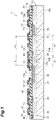
- FIG. 1 is a schematic cross-sectional view of a light detection device.
- FIG. 2 is a plan view of the light detection device.
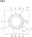
- FIG. 3 is a schematic plan view of a semiconductor substrate included in the light detection device.
- the semiconductor substrate 10 includes an APD 11 and a temperature compensation diode 12.
- the APD 11 and the temperature compensation diode 12 have the same temperature characteristics with respect to the relationship between the amplification factor and the bias voltage.
- the breakdown voltage of the APD 11 and the breakdown voltage of the temperature compensation diode 12 are different.
- the breakdown voltage of the APD 11 is higher than the breakdown voltage of the temperature compensation diode 12.
- the breakdown voltage of the temperature compensation diode 12 is applied to the APD 11 as a bias voltage.
- the APD 11 and the temperature compensation diode 12 have the same temperature characteristics with respect to the relationship between the amplification factor and the bias voltage.
- the breakdown voltage applied to the temperature compensation diode 12 changes.
- the bias voltage applied to the APD 11 also changes according to the ambient temperature so that the amplification factor of the APD 11 is maintained. That is, in the light detection device 1, the temperature compensation diode 12 provides temperature compensation for the amplification factor of the APD 11.
- the semiconductor substrate 10 has main surfaces 10a and 10b facing each other.
- the APD 11 and the temperature compensation diode 12 are formed on the semiconductor substrate 10 so as to be spaced apart from each other when viewed from a direction perpendicular to the main surface 10a.
- the APD 11 has a light incidence surface 11a on the main surface 10a side.
- the temperature compensation diode 12 is a light-shielded APD.
- the semiconductor substrate 10 includes a peripheral carrier absorbing portion 13 in addition to the APD 11 and the temperature compensation diode 12.
- a part of the peripheral carrier absorbing portion 13 is located between the APD 11 and the temperature compensation diode 12 when viewed from the direction perpendicular to the main surface 10a.
- the peripheral carrier absorbing portion 13 surrounds the APD 11.
- the peripheral carrier absorbing portion 13 is a region that absorbs carriers located at the periphery.
- the semiconductor substrate 10 includes a semiconductor region 21 and semiconductor layers 31, 32, 33, 34, and 35.
- Each of the APD 11 and the temperature compensation diode 12 includes the semiconductor region 21 and the semiconductor layers 31, 32, and 35.
- the peripheral carrier absorbing portion 13 includes the semiconductor region 21 and the semiconductor layers 33 and 35.
- the peripheral carrier absorbing portion 13 absorbs carriers located at the periphery in the semiconductor layer 33. That is, the semiconductor layer 33 functions as a peripheral carrier absorbing layer that absorbs peripheral carriers.
- the peripheral carrier absorbing portion 13 is a portion of the semiconductor substrate 10 surrounded by edges 13a and 13b of the peripheral carrier absorbing layer when viewed from the direction perpendicular to the main surface 10a.
- the edges 13a and 13b are edges of the semiconductor layer 33. The edge 13b is located closer to the APD 11 than the edge 13a.
- the semiconductor region 21 and the semiconductor layers 32, 34, and 35 are the first conductivity type, and the semiconductor layers 31 and 33 are the second conductivity type.
- Semiconductor impurities are added by, for example, a diffusion method or an ion implantation method.
- the first conductivity type is P type and the second conductivity type is N type.
- the semiconductor substrate 10 is an Si-based substrate, a Group 13 element such as B is used as the P-type impurity, and a Group 15 element such as N, P, or As is used as the N-type impurity.
- the semiconductor region 21 is located on the main surface 10a side of the semiconductor substrate 10.
- the semiconductor region 21 forms a part of the main surface 10a.
- the semiconductor region 21 is, for example, P - type.
- the semiconductor layer 31 forms a part of the main surface 10a.
- the semiconductor layer 31 is surrounded by the semiconductor region 21 so as to be in contact with the semiconductor region 21 when viewed from the direction perpendicular to the main surface 10a.
- the semiconductor layer 31 is, for example, N + type.
- the semiconductor layer 31 forms a cathode in each of the APD 11 and the temperature compensation diode 12.
- the semiconductor layer 32 is located between the semiconductor region 21 and the semiconductor layer 31. In other words, the semiconductor layer 32 is in contact with the semiconductor layer 31 on the main surface 10a side and is in contact with the semiconductor region 21 on the main surface 10b side.
- the semiconductor layer 32 has a higher impurity concentration than the semiconductor region 21.
- the semiconductor layer 32 is, for example, P type.
- the impurity concentration of the semiconductor layer 32 of the temperature compensation diode 12 is higher than the impurity concentration of the semiconductor layer 32 of the APD 11.
- the semiconductor layer 32 forms an avalanche region in each of the APD 11 and the temperature compensation diode 12.
- the semiconductor layer 33 forms a part of the main surface 10a.
- the semiconductor layer 33 is surrounded by the semiconductor region 21 so as to be in contact with the semiconductor region 21 when viewed from the direction perpendicular to the main surface 10a.
- the peripheral carrier absorbing portion 13 includes the semiconductor layer 33, and is in contact with only the semiconductor region 21 of the semiconductor substrate 10.
- the peripheral carrier absorbing portion 13 does not include a layer corresponding to the avalanche region.
- the semiconductor layer 33 has the same impurity concentration as the semiconductor layer 31.
- the semiconductor layer 33 is, for example, N + type.
- the semiconductor layer 34 forms a part of the main surface 10a.
- the semiconductor layer 34 is surrounded by the semiconductor region 21 so as to be in contact with the semiconductor region 21 when viewed from the direction perpendicular to the main surface 10a.
- the semiconductor layer 34 has a higher impurity concentration than the semiconductor region 21 and the semiconductor layer 32.
- the semiconductor layer 34 is, for example, P + type.
- the semiconductor layer 34 is connected to the semiconductor layer 35 at a portion that is not illustrated.
- the semiconductor layer 34 forms an anode of the light detection device 1.
- the semiconductor layer 34 forms, for example, anodes of the APD 11, the temperature compensation diode 12, and the peripheral carrier absorbing portion 13.
- the semiconductor layer 35 is located closer to the main surface 10b of the semiconductor substrate 10 than the semiconductor region 21.
- the semiconductor layer 35 forms the entire main surface 10b.
- the semiconductor layer 35 is in contact with the semiconductor region 21 on the main surface 10a side.
- the semiconductor layer 35 has a higher impurity concentration than the semiconductor region 21 and the semiconductor layer 32.
- the semiconductor layer 35 is, for example, P + type.
- the semiconductor layer 35 forms an anode of the light detection device 1.
- the semiconductor layer 35 forms, for example, anodes of the APD 11, the temperature compensation diode 12, and the peripheral carrier absorbing portion 13.
- the light detection device 1 further includes an insulating film 41, electrodes 42, 43, 44, and 45, a passivation film 46, and an antireflection film 47 that are provided on the main surface 10a of the semiconductor substrate 10.
- the insulating film 41 is stacked on the main surface 10a of the semiconductor substrate 10.
- the insulating film 41 is, for example, a silicon oxide film.
- Each of the electrodes 42, 43, 44, and 45 is disposed on the insulating film 41.
- the passivation film 46 is stacked on the insulating film 41 and the electrodes 42, 43, 44, and 45.
- the antireflection film 47 is stacked on the main surface 10a of the semiconductor substrate 10.
- the electrode 42 penetrates the insulating film 41 to be connected to the semiconductor layer 31 of the APD 11. A part of the electrode 42 is exposed from the passivation film 46 to form a pad electrode 52 of the APD 11. The electrode 42 outputs a signal from the APD 11 at the pad electrode 52.
- the electrode 43 penetrates the insulating film 41 to be connected to the semiconductor layer 31 of the temperature compensation diode 12. A part of the electrode 43 is exposed from the passivation film 46 to form, for example, a pad electrode 53 of the temperature compensation diode 12.
- the electrode 44 penetrates the insulating film 41 to be connected to the semiconductor layer 33 of the peripheral carrier absorbing portion 13. A part of the electrode 44 is exposed from the passivation film 46 to form, for example, a pad electrode 54 of the peripheral carrier absorbing portion 13.
- the electrode 45 penetrates the insulating film 41 to be connected to the semiconductor layer 34. That is, the electrode 45 is connected to the APD 11, the temperature compensation diode 12, and the peripheral carrier absorbing portion 13. In other words, the APD 11, the temperature compensation diode 12, and the peripheral carrier absorbing portion 13 are connected to the electrode 45 in parallel with each other. A part of the electrode 45 is exposed from the passivation film 46 to form, for example, a pad electrode 55.
- the pad electrodes 52, 53, 54, 55 are disposed around the APD 11 as illustrated in FIG. 2 when the light detection device 1 is viewed from the direction perpendicular to the main surface 10a.
- the pad electrode 52 is a pad electrode for the cathode of the APD 11.
- the pad electrode 53 is a pad electrode for the cathode of the temperature compensation diode 12.
- the pad electrode 54 is a pad electrode for the cathode of the peripheral carrier absorbing portion 13.
- the pad electrode 55 is a pad electrode for the anodes of the APD 11, the temperature compensation diode 12, and the peripheral carrier absorbing portion 13.
- the APD 11, the temperature compensation diode 12, and the peripheral carrier absorbing portion 13 are connected to the pad electrode 55 in parallel with each other.
- a reverse bias is applied to the APD 11, the temperature compensation diode 12, and the peripheral carrier absorbing portion 13, a positive voltage is applied to the pad electrode for the cathode, and a negative voltage is applied to the pad electrode for the anode.
- the antireflection film 47 is stacked on the semiconductor layer 31 of the APD 11. A part of the antireflection film 47 is exposed from the passivation film 46. Therefore, light transmitted through the antireflection film 47 can enter the semiconductor layer 31 of the APD 11.
- the semiconductor layer 31 of the temperature compensation diode 12 and the semiconductor layer 33 of the peripheral carrier absorbing portion 13 are covered with the insulating film 41 and are shielded from light. Therefore, when the light detection device 1 is viewed from the main surface 10a side in the direction perpendicular to the main surface 10a, the semiconductor layer 31 of the APD 11 is visible as illustrated in FIG. 2 .
- the semiconductor layer 31 of the temperature compensation diode 12 and the semiconductor layer 33 of the peripheral carrier absorbing portion 13 are not visible.
- FIG. 3 is a schematic plan view of the semiconductor substrate 10 viewed from the main surface 10a side in the direction perpendicular to the main surface 10a.
- the semiconductor layer 31 of the APD 11 and the semiconductor layer 31 of the temperature compensation diode 12 have a circular shape when viewed from the direction perpendicular to the main surface 10a.
- the semiconductor layer 33 of the peripheral carrier absorbing portion 13 has an annular shape when viewed from the direction perpendicular to the main surface 10a, and surrounds the semiconductor layer 31 so as to be spaced apart from the semiconductor layer 31 of the APD 11.
- a part of the semiconductor layer 33 is located between the semiconductor layer 31 of the APD 11 and the semiconductor layer 31 of the temperature compensation diode 12 when viewed from the direction perpendicular to the main surface 10a.
- the peripheral carrier absorbing portion 13 is located between the APD 11 and the temperature compensation diode 12 when viewed from the direction perpendicular to the main surface 10a.
- the shortest distance between the APD 11 and the peripheral carrier absorbing portion 13 is smaller than the shortest distance between a portion 13c of the peripheral carrier absorbing portion 13 and the temperature compensation diode 12.
- the portion 13c is a portion, which is closest to the APD 11, of the edges 13a and 13b of the peripheral carrier absorbing portion 13 on the line segment connecting the APD 11 and the temperature compensation diode 12 to each other at the shortest distance.
- the portion 13c is a portion, which is closest to the temperature compensation diode 12, of the edge 13b of the peripheral carrier absorbing portion 13 when viewed from the direction perpendicular to the main surface 10a.
- the distance L1 when viewed from the direction perpendicular to the main surface 10a, the distance L1 is smaller than the distance L2 on the line segment connecting the semiconductor layer 31 of the APD 11 and the semiconductor layer 31 of the temperature compensation diode 12 to each other at the shortest distance.
- the distance L1 is the shortest distance between the semiconductor layer 31 of the APD 11 and the peripheral carrier absorbing portion 13 when viewed from the direction perpendicular to the main surface 10a.
- the distance L2 is the shortest distance between the portion 13c of the peripheral carrier absorbing portion 13 and the semiconductor layer 31 of the temperature compensation diode 12 when viewed from the direction perpendicular to the main surface 10a.
- L2/L1 is, for example, more than 1 and 50 or less. L2/L1 may be 20 or more and 50 or less.
- the distance L3 when viewed from the direction perpendicular to the main surface 10a, the distance L3 is smaller than the distance L4 on the line segment connecting the semiconductor layer 32 of the APD 11 and the semiconductor layer 32 of the temperature compensation diode 12 to each other at the shortest distance.
- the distance L3 is the shortest distance between the semiconductor layer 32 of the APD 11 and the peripheral carrier absorbing portion 13 when viewed from the direction perpendicular to the main surface 10a.
- the distance L4 is the shortest distance between the portion 13c of the peripheral carrier absorbing portion 13 and the semiconductor layer 32 of the temperature compensation diode 12 when viewed from the direction perpendicular to the main surface 10a.
- the light detection device 1 is used in a state in which a power supply 61 and a current limiting circuit 62 are connected to the pad electrode 55.
- the positive electrode side of the power supply 61 is connected to the ground 63, and the negative electrode side of the power supply 61 is connected to the pad electrode 55 through the current limiting circuit 62.
- the pad electrodes 53 and 54 are connected to the grounds 64 and 65, respectively.
- the grounds 64 and 65 may be connected to each other.
- the pad electrode 52 is connected to a signal reading circuit (not illustrated).
- the pad electrode 55 is connected to the semiconductor layer 34 of the P + type, and the semiconductor layer 34 is connected to the semiconductor layer 35 of the P + type. Therefore, the anodes of the APD 11, the temperature compensation diode 12, and the peripheral carrier absorbing portion 13 are connected to the pad electrode 55 in parallel with each other. As a result, a negative potential is applied to the anodes of the APD 11, the temperature compensation diode 12, and the peripheral carrier absorbing portion 13 by the power supply 61.
- the difference between the potential applied to the pad electrode 53 and the potential applied to the pad electrode 55 is a breakdown voltage of the temperature compensation diode 12. Therefore, a potential corresponding to the breakdown voltage applied to the temperature compensation diode 12 is applied to the anode of the APD 11. As a result, a voltage corresponding to the breakdown voltage applied to the temperature compensation diode 12 is applied to the APD 11 as a bias voltage. Similarly, a voltage corresponding to the breakdown voltage applied to the temperature compensation diode 12 is applied to the anode of the peripheral carrier absorbing portion 13 as a bias voltage.
- the breakdown voltage of the temperature compensation diode 12 is applied to the pad electrode 55. Therefore, the breakdown voltage of the temperature compensation diode 12 is applied to the APD 11 and the peripheral carrier absorbing portion 13 as a bias voltage.
- the output voltage of the power supply 61 is equal to or higher than the operating voltage of the APD 11. In other words, the output voltage of the power supply 61 is equal to or higher than the upper limit of the temperature fluctuation of the breakdown voltage of the temperature compensation diode 12. For example, the output voltage of the power supply 61 is 300 V or higher.
- the current limiting circuit 62 is configured to include, for example, a current mirror circuit or a resistor.
- the multiplication factor of the APD 11 can be arbitrarily set according to the breakdown voltage difference between the temperature compensation diode 12 and the APD 11.
- the amplification factor of the APD 11 is set to an optimal multiplication factor Mopt having a high S/N ratio, the detection accuracy can be improved.
- the anodes of the APD 11, the temperature compensation diode 12, and the peripheral carrier absorbing portion 13 are integrally formed in the semiconductor layer 35.
- the potential applied to the pad electrode 53 is 0 V and the breakdown voltage of the temperature compensation diode 12 is 130 V under an ambient temperature of 25°C
- a potential of -130 V is applied to the anode of the APD 11 and the anode of the peripheral carrier absorbing portion 13. Therefore, when the breakdown voltage of the APD 11 is 150 V under an ambient temperature of 25°C, the APD 11 operates in a state in which the potential difference between the anode and the cathode is lower by 20 V than the breakdown voltage.
- the APD 11 and the temperature compensation diode 12 have the same temperature characteristics with respect to the relationship between the amplification factor and the bias voltage. Therefore, as long as the temperature compensation diode 12 is in a breakdown state, the APD 11 operates while maintaining the amplification factor when a bias voltage lower by 20 V than the breakdown voltage is applied under an ambient temperature of 25°C. In other words, in the light detection device 1, since a voltage that causes the temperature compensation diode 12 to break down is applied to the temperature compensation diode 12, temperature compensation is provided for the amplification factor of the APD 11.
- the light detection device 1 may have a configuration in which the reach-through type APD 11 arranged to operate in Geiger mode.
- a quenching resistor is connected to the APD 11.
- the semiconductor substrate 10 is configured such that the impurity concentration of the semiconductor layer 32 of the temperature compensation diode 12 is lower than the impurity concentration of the semiconductor layer 32 of the APD 11.
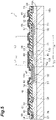
- FIG. 5 is a schematic cross-sectional view of the light detection device according to the modification example.
- FIG. 6 is a schematic plan view of a semiconductor substrate illustrated in FIG. 5 .
- This modification example is generally similar to or the same as the above-described embodiment.
- This modification example is different from the above-described embodiment in that the semiconductor layer 31 of the temperature compensation diode 12 and the semiconductor layer 33 of the peripheral carrier absorbing portion 13 are connected by semiconductor layers of the same conductivity type as the semiconductor layers 31 and 33.
- the differences between the above-described embodiment and the modification example will be mainly described.
- a semiconductor substrate 10A includes a semiconductor layer 71 that connects the semiconductor layer 31 of the temperature compensation diode 12 and the semiconductor layer 33 of the peripheral carrier absorbing portion 13 to each other.
- the semiconductor layer 71 has the same conductivity type as the semiconductor layers 31 and 33.
- the semiconductor layer 71 is the same second conductivity type as the semiconductor layers 31 and 33, and is located at the same height as the semiconductor layers 31 and 33 in the thickness direction of the semiconductor substrate 10.
- the semiconductor layer 71 is, for example, N + type.
- the semiconductor layer 31 of the APD 11 and the semiconductor layer 31 of the temperature compensation diode 12 have a circular shape when viewed from the direction perpendicular to the main surface 10a.
- the semiconductor layer 33 of the peripheral carrier absorbing portion 13 has an annular shape when viewed from the direction perpendicular to the main surface 10a, and surrounds the semiconductor layer 31 so as to be spaced apart from the semiconductor layer 31 of the APD 11.
- a part of the semiconductor layer 33 is located between the semiconductor layer 31 of the APD 11 and the semiconductor layer 31 of the temperature compensation diode 12 when viewed from the direction perpendicular to the main surface 10a.
- the peripheral carrier absorbing portion 13 is located between the APD 11 and the temperature compensation diode 12 when viewed from the direction perpendicular to the main surface 10a.
- the semiconductor layer 71 connects the edge 13a of the peripheral carrier absorbing portion 13 and the semiconductor layer 33 of the temperature compensation diode 12 to each other between the semiconductor layer 31 of the APD 11 and the semiconductor layer 31 of the temperature compensation diode 12 when viewed from the direction perpendicular to the main surface 10a.
- the semiconductor layer 71 and the semiconductor layer 31 of the temperature compensation diode 12 are integrated to the extent that the boundary cannot be recognized.
- the semiconductor layer 71 and the semiconductor layer 33 of the peripheral carrier absorbing portion 13 are integrated to the extent that the boundary cannot be recognized.
- FIG. 7 is a schematic plan view of a semiconductor substrate of the light detection device according to this modification example.
- This modification example is generally similar to or the same as the above-described embodiment.
- This modification example is different from the above-described embodiment in that the light detection device includes a semiconductor substrate on which an APD array including a plurality of APDs is formed.
- the differences between the above-described embodiment and the modification example will be mainly described.
- a semiconductor substrate 10B illustrated in FIG. 7 includes an APD array 80 including a plurality of APDs 81, a temperature compensation diode 82, and a peripheral carrier absorbing portion 83 on the main surface 10a side.
- the APD array 80 is formed on the semiconductor substrate 10B so as to be spaced apart from the temperature compensation diode 82 and the peripheral carrier absorbing portion 83 when viewed from the direction perpendicular to the main surface 10a.
- the APDs 81 are formed on the semiconductor substrate 10B so as to be spaced apart from each other when viewed from the direction perpendicular to the main surface 10a.
- the plurality of APDs 81 and the temperature compensation diodes 82 have rectangular shapes with an equal size, and are arranged in a row in one direction. In the semiconductor substrate 10B, the plurality of APDs 81 are arranged at equal intervals.
- the temperature compensation diode 82 is located at the end of the array of the plurality of APDs 81 and the temperature compensation diode 82.
- the peripheral carrier absorbing portion 83 surrounds the plurality of APDs 81 when viewed from the direction perpendicular to the main surface 10a.
- a part of the peripheral carrier absorbing portion 83 is located between the APD array 80 and the temperature compensation diode 82 when viewed from the direction perpendicular to the main surface 10a.
- a part of the peripheral carrier absorbing portion 83 is located between the temperature compensation diode 82 and an APD 81a closest to the temperature compensation diode 82, among the plurality of APDs 81, when viewed from the direction perpendicular to the main surface 10a.
- Each of the APD 81 and the temperature compensation diode 82 includes a semiconductor region 21 and semiconductor layers 31, 32, and 35, similarly to the APD 11 and the temperature compensation diode 12 in the embodiment described above.
- the peripheral carrier absorbing portion 83 includes the semiconductor region 21 and the semiconductor layers 33 and 35.
- the semiconductor layer 33 of the peripheral carrier absorbing portion 83 has an annular shape when viewed from the direction perpendicular to the main surface 10a.
- the peripheral carrier absorbing portion 83 absorbs carriers located at the periphery in the semiconductor layer 33. That is, the semiconductor layer 33 functions as a peripheral carrier absorbing layer that absorbs peripheral carriers.
- the peripheral carrier absorbing portion 83 stands for a portion of the semiconductor substrate 10B surrounded by edges 83a and 83b of the peripheral carrier absorbing layer when viewed from the direction perpendicular to the main surface 10a.
- the edges 83a and 83b are edges of the semiconductor layer 33.
- the edge 83b is located closer to the APD 81 than the edge 83a.
- the shortest distance between the APD 81a and the peripheral carrier absorbing portion 83 is smaller than the shortest distance between a portion 83c of the peripheral carrier absorbing portion 83 and the temperature compensation diode 82.
- the portion 83c is a portion, which is closest to the APD 81a, of the edges 83a and 83b of the peripheral carrier absorbing portion 83 on the line segment connecting the APD 81a and the temperature compensation diode 82 to each other at the shortest distance.
- the portion 83c is a portion, which is closest to the temperature compensation diode 82, of the edge 83b of the peripheral carrier absorbing portion 83 when viewed from the direction perpendicular to the main surface 10a.
- the distance L1 is smaller than the distance L2 on the line segment connecting the semiconductor layer 31 of the APD 81a and the semiconductor layer 31 of the temperature compensation diode 82 to each other at the shortest distance.
- the distance L1 is the shortest distance between the semiconductor layer 31 of the APD 81a and the peripheral carrier absorbing portion 83 when viewed from the direction perpendicular to the main surface 10a.
- the distance L2 is the shortest distance between the portion 83c of the peripheral carrier absorbing portion 83 and the semiconductor layer 31 of the temperature compensation diode 82 when viewed from the direction perpendicular to the main surface 10a.
- L2/L1 is, for example, more than 1 and 50 or less. L2/L1 may be 20 or more and 50 or less.
- the distance L3 is smaller than the distance L4 on the line segment connecting the semiconductor layer 32 of the APD 81a and the semiconductor layer 32 of the temperature compensation diode 82 to each other at the shortest distance.
- the distance L3 is the shortest distance between the semiconductor layer 32 of the APD 81a and the peripheral carrier absorbing portion 83 when viewed from the direction perpendicular to the main surface 10a.
- the distance L4 is the shortest distance between the portion 83c of the peripheral carrier absorbing portion 83 and the semiconductor layer 32 of the temperature compensation diode 82 when viewed from the direction perpendicular to the main surface 10a.
- FIG. 8 is a schematic cross-sectional view of the light detection device according to the modification example.
- This modification example is generally similar to or the same as the above-described embodiment.
- This modification example is different from the above-described embodiment in that a so-called reverse type APD is formed on the semiconductor substrate of the light detection device and that the APD on the semiconductor substrate is arranged to operate in Geiger mode.
- the semiconductor substrate 10 illustrated in FIG. 1 has a so-called reach-through type APD, and the APD operates in the linear mode.
- a semiconductor substrate 10C of a light detection device 1C according to this modification example has a so-called reverse type APD, and the APD is arranged to operate in Geiger mode.
- the differences between the above-described embodiment and the modification example will be mainly described.
- the semiconductor substrate 10C includes an APD 91, a temperature compensation diode 92, and a peripheral carrier absorbing portion 93 respectively corresponding to the APD 11, the temperature compensation diode 12, and the peripheral carrier absorbing portion 13 of the semiconductor substrate 10.
- the APD 91 has a light incidence surface 91a corresponding to the light incidence surface 11a of the APD 11 on the main surface 10a side.
- the semiconductor substrate 10C includes a semiconductor region 21 and semiconductor layers 31, 33, 34, 35, and 36.
- the semiconductor substrate 10C is different from the semiconductor substrate 10 in that the semiconductor layer 36 is provided instead of the semiconductor layer 32.
- Each of the APD 91 and the temperature compensation diode 92 includes the semiconductor region 21 and the semiconductor layers 31, 35, and 36. As illustrated in FIG. 8 , the semiconductor layer 34 is in contact with the semiconductor layer 35.
- the peripheral carrier absorbing portion 93 includes the semiconductor region 21 and the semiconductor layers 33 and 35.
- the peripheral carrier absorbing portion 93 absorbs carriers located at the periphery in the semiconductor layer 33. That is, the semiconductor layer 33 functions as a peripheral carrier absorbing layer that absorbs peripheral carriers.
- the peripheral carrier absorbing portion 93 is a portion of the semiconductor substrate 10C surrounded by edges 93a and 93b of the peripheral carrier absorbing layer when viewed from the direction perpendicular to the main surface 10a.
- the edges 93a and 93b are edges of the semiconductor layer 33.
- the edge 93b is located closer to the APD 91 than the edge 93a.
- the semiconductor layer 36 is located between the semiconductor region 21 and the semiconductor layer 35.
- the semiconductor layer 36 is in contact with the semiconductor region 21 on the main surface 10a side and is in contact with the semiconductor layer 35 on the main surface 10b side.
- the impurity concentration of the semiconductor layer 36 of the temperature compensation diode 92 is lower than the impurity concentration of the semiconductor layer 36 of the APD 91.
- the semiconductor region 21 and the semiconductor layers 31, 33, and 36 are the first conductivity type, and the semiconductor layers 34, and 35 are the second conductivity type.
- the first conductivity type is P type and the second conductivity type is N type.
- the semiconductor substrate 10C is an Si-based substrate, a Group 13 element such as B is used as the P-type impurity, and a Group 15 element such as N, P, or As is used as the N-type impurity.
- the semiconductor layers 31 and 33 have a higher impurity concentration than the semiconductor region 21.
- the semiconductor layer 36 has a higher impurity concentration than the semiconductor region 21, and has a lower impurity concentration than the semiconductor layers 31 and 33.
- the semiconductor region 21 is, for example, P - type
- the semiconductor layers 31 and 33 are, for example, P + type
- the semiconductor layer 36 is, for example, P type.
- the semiconductor layer 31 forms an anode in each of the APD 91 and the temperature compensation diode 92.
- the semiconductor layer 34 has the same impurity concentration as the semiconductor layer 35.
- the semiconductor layers 34 and 35 are, for example, N + type.
- the semiconductor layers 34 and 35 form the cathode of the light detection device 1C.
- the semiconductor layers 34 and 35 form, for example, cathodes of the APD 91, the temperature compensation diode 92, and the peripheral carrier absorbing portion 93.
- a quenching resistor 95 is provided in a part of the electrode 42.
- the quenching resistor 95 is electrically connected to the semiconductor layer 31 of the P + type in the APD 91.
- the quenching resistor 95 is electrically connected to the pad electrode 52 on a side opposite to the semiconductor layer 31.
- the pad electrode 52 is a pad electrode for the anode of the APD 91.
- the pad electrode 53 is a pad electrode for the anode of the temperature compensation diode 92.
- the pad electrode 54 is a pad electrode for the anode of the peripheral carrier absorbing portion 93.
- the pad electrode 55 is a pad electrode for the cathodes of the APD 91, the temperature compensation diode 92, and the peripheral carrier absorbing portion 93.
- the APD 91, the temperature compensation diode 92, and the peripheral carrier absorbing portion 93 are connected to the pad electrode 55 in parallel with each other.
- a reverse bias is applied to the APD 91, the temperature compensation diode 92, and the peripheral carrier absorbing portion 93, a positive voltage is applied to the pad electrode for the anode, and a negative voltage is applied to the pad electrode for the cathode.
- the shortest distance between the APD 91 and the peripheral carrier absorbing portion 93 is smaller than the shortest distance between a portion 93c of the peripheral carrier absorbing portion 93 and the temperature compensation diode 92.
- the portion 93c is a portion, which is closest to the APD 91, of the edges 93a and 93b of the peripheral carrier absorbing portion 93 on the line segment connecting the APD 91 and the temperature compensation diode 92 to each other at the shortest distance.
- the portion 93c is a portion, which is closest to the temperature compensation diode 92, of the edge 93b of the peripheral carrier absorbing portion 93 when viewed from the direction perpendicular to the main surface 10a.
- the distance L1 when viewed from the direction perpendicular to the main surface 10a, the distance L1 is smaller than the distance L2 on the line segment connecting the semiconductor layer 31 of the APD 91 and the semiconductor layer 31 of the temperature compensation diode 92 to each other at the shortest distance.
- the distance L1 is the shortest distance between the semiconductor layer 31 of the APD 91 and the peripheral carrier absorbing portion 93 when viewed from the direction perpendicular to the main surface 10a.
- the distance L2 is the shortest distance between the portion 93c of the peripheral carrier absorbing portion 93 and the semiconductor layer 31 of the temperature compensation diode 92 when viewed from the direction perpendicular to the main surface 10a.
- L2/L1 is, for example, more than 1 and 50 or less. L2/L1 may be 20 or more and 50 or less.
- the distance L3 when viewed from the direction perpendicular to the main surface 10a, the distance L3 is smaller than the distance L4 on the line segment connecting the semiconductor layer 36 of the APD 91 and the semiconductor layer 36 of the temperature compensation diode 92 to each other at the shortest distance.
- the distance L3 is the shortest distance between the semiconductor layer 36 of the APD 91 and the peripheral carrier absorbing portion 93 when viewed from the direction perpendicular to the main surface 10a.
- the distance L4 is the shortest distance between the portion 93c of the peripheral carrier absorbing portion 93 and the semiconductor layer 36 of the temperature compensation diode 92 when viewed from the direction perpendicular to the main surface 10a.
- the light detection device 1C is used in a state in which the power supply 61 and the current limiting circuit 62 are connected to the pad electrode 55.
- the negative electrode side of the power supply 61 is connected to the ground 63
- the positive electrode side of the power supply 61 is connected to the pad electrode 55 through the current limiting circuit 62.
- the pad electrodes 53 and 54 are connected to the grounds 64 and 65, respectively.
- the grounds 64 and 65 may be connected to each other.
- the pad electrode 52 is connected to a signal reading circuit (not illustrated).
- the pad electrode 55 is connected to the semiconductor layer 34 of the N + type, and the semiconductor layer 34 is connected to the semiconductor layer 35 of the N + type. Therefore, the cathodes of the APD 91, the temperature compensation diode 92, and the peripheral carrier absorbing portion 93 are connected to the pad electrode 55 in parallel with each other. As a result, a positive potential is applied to the cathodes of the APD 91, the temperature compensation diode 92, and the peripheral carrier absorbing portion 93 by the power supply 61.
- the difference between the potential applied to the pad electrode 53 and the potential applied to the pad electrode 55 is a breakdown voltage of the temperature compensation diode 92. Therefore, a potential corresponding to the breakdown voltage applied to the temperature compensation diode 92 is applied to the cathode of the APD 91. As a result, a voltage corresponding to the breakdown voltage applied to the temperature compensation diode 92 is applied to the APD 91 as a bias voltage. Similarly, a voltage corresponding to the breakdown voltage applied to the temperature compensation diode 92 is applied to the cathode of the peripheral carrier absorbing portion 93 as a bias voltage.
- the breakdown voltage of the temperature compensation diode 92 is applied to the pad electrode 55. Therefore, the breakdown voltage of the temperature compensation diode 92 is applied to the APD 91 and the peripheral carrier absorbing portion 93 as a bias voltage.
- the output voltage of the power supply 61 is equal to or higher than the operating voltage of the APD 91. In other words, the output voltage of the power supply 61 is equal to or higher than the upper limit of the temperature fluctuation of the breakdown voltage of the temperature compensation diode 92.
- the output voltage of the power supply 61 is 300 V or higher.
- the current limiting circuit 62 is configured to include, for example, a current mirror circuit or a resistor.
- the multiplication factor of the APD 91 can be arbitrarily set according to the breakdown voltage difference between the temperature compensation diode 92 and the APD 91.
- the amplification factor of the APD 91 is set to the optimal multiplication factor Mopt having a high S/N ratio, the detection accuracy can be improved.
- the cathodes of the APD 91, the temperature compensation diode 92, and the peripheral carrier absorbing portion 93 are integrally formed in the semiconductor layer 35.
- the potential applied to the pad electrode 53 is 0 V and the breakdown voltage of the temperature compensation diode 12 is 50 V under an ambient temperature of 25°C
- a potential of +50 V is applied to the cathode of the APD 91 and the cathode of the peripheral carrier absorbing portion 13.
- the breakdown voltage of the APD 91 is 48 V under an ambient temperature of 25°C
- the APD 91 operates in a state in which the potential difference between the anode and the cathode is higher by 2V than the breakdown voltage.
- the APD 91 and the temperature compensation diode 92 have the same temperature characteristics with respect to the relationship between the amplification factor and the bias voltage. Therefore, as long as the temperature compensation diode 92 is in a breakdown state, the APD 91 operates while maintaining the amplification factor when a bias voltage higher by 2 V than the breakdown voltage is applied under an ambient temperature of 25°C. In other words, in the light detection device 1C, since a voltage that causes the temperature compensation diode 92 to break down is applied to the temperature compensation diode 92, temperature compensation is provided for the amplification factor of the APD 91.
- the light detection device 1C may have a configuration in which the reverse type APD 91 operates in the linear mode. In the configuration in which the APD 91 operates in the linear mode, the quenching resistor 95 is not required.
- the semiconductor substrate 10C is configured such that the impurity concentration of the semiconductor layer 36 of the temperature compensation diode 92 is higher than the impurity concentration of the semiconductor layer 36 of the APD 91.
- the operational effects of the light detection devices in the above-described embodiment and modification examples will be described.
- a light detection device including an APD and a temperature compensation diode having the same temperature characteristics it has been necessary to select and combine APDs having desired temperature characteristics with respect to the relationship between the amplification factor and the bias voltage. For this reason, it has been difficult to reduce the cost.
- the APDs 11, 81, and 91 and the temperature compensation diodes 12, 82, and 92 are formed on the same semiconductor substrates 10, 10A, 10B, and 10C, respectively.
- the temperature compensation diodes 12, 82, and 92 and the APDs 11, 81, and 91 having the same temperature characteristics over a wide temperature range with respect to the amplification factor and the bias voltage are formed more easily and accurately than in a case where the temperature compensation diodes 12, 82, and 92 and the APDs 11, 81, and 91 are formed on different semiconductor substrates. Therefore, temperature compensation can be ensured for the multiplication factor while suppressing the manufacturing cost.
- the temperature compensation diodes 12, 82, and 92 may emit light.
- the temperature compensation diodes 12, 82, and 92 emit light, carriers are generated in the semiconductor substrate due to the light emitted from the temperature compensation diodes 12, 82, and 92. Therefore, in a state in which the temperature compensation diodes 12, 82, and 92 and the APDs 11, 81, and 91 are formed on the same semiconductor substrate, the carriers may affect the detection results of the APDs 11, 81, and 91.
- the peripheral carrier absorbing portions 13, 83, and 93 are located between the APDs 11, 81, and 91 and the temperature compensation diodes 12, 82, and 92.
- the shortest distances between the APDs 11, 81, and 91 and the peripheral carrier absorbing portions 13, 83, and 93 are smaller than the shortest distances between the portions 13c, 83c, and 93c of the peripheral carrier absorbing portions 13, 83, and 93 and the temperature compensation diodes 12, 82, and 92.
- the distances L1 between the semiconductor layers 31 of the APDs 11, 81, and 91 and the peripheral carrier absorbing portions 13, 83, and 93 are smaller than the distances L2 between the portions 13c, 83c, and 93c of the peripheral carrier absorbing portions 13, 83, and 93 and the semiconductor layers 31 of the temperature compensation diodes 12, 82, and 92.
- the distances L3 between the semiconductor layers 32 of the APDs 11 and 81 and the peripheral carrier absorbing portions 13 and 83 are smaller than the distances L4 between the portions 13c and 83c of the peripheral carrier absorbing portions 13 and 83 and the semiconductor layers 32 of the temperature compensation diodes 12 and 82.
- the distance L3 between the semiconductor layer 36 of the APD 91 and the peripheral carrier absorbing portions 93 is smaller than the distance L4 between the portion 93c of the peripheral carrier absorbing portion 93 and the semiconductor layer 36 of the temperature compensation diode 92.
- the carriers generated due to the light emission of the temperature compensation diodes 12, 82, and 92 are absorbed at the peripheral carrier absorbing portions 13, 83, and 93 before reaching the APDs 11, 81, and 91.
- the carriers due to the temperature compensation diodes 12, 82, and 92 are suppressed from reaching the APDs 11, 81, and 91, enabling improvement of the detection accuracy. Therefore, in the light detection devices 1 and 1C, temperature compensation is ensured for the multiplication factor while suppressing the manufacturing cost, enabling improvement of the detection accuracy.
- L2/L1 is, for example, more than 1 and 50 or less.
- L2/L1 may be 20 or more and 50 or less, and in this case, the carriers due to the temperature compensation diodes 12, 82, and 92 are further suppressed from reaching the APDs 11, 81, and 91.
- the light detection devices 1 and 1C include the electrodes 42, 43, 44, and 45.
- the electrode 42 is connected to the APDs 11, 81, and 91 and is configured to output signals from the APDs 11, 81, and 91.
- the electrode 43 is connected to the temperature compensation diodes 12, 82, and 92, and the electrode 44 is connected to the peripheral carrier absorbing portions 13, 83, and 93. Therefore, a desired potential can be applied to each of the APDs 11, 81, and 91, the temperature compensation diodes 12, 82, and 92, and the peripheral carrier absorbing portions 13, 83, and 93.
- a voltage is applied to the peripheral carrier absorbing portions 13, 83, and 93, the carriers generated in the temperature compensation diodes 12, 82, and 92 can be further absorbed.
- the APDs 11, 81, and 91, the temperature compensation diodes 12, 82, and 92, and the peripheral carrier absorbing portions 13, 83, and 93 are connected to the electrode 45 in parallel with each other. Since the APDs 11, 81, and 91 and the temperature compensation diodes 12, 82, and 92 are connected in parallel to each other, potentials corresponding to the breakdown voltages of the temperature compensation diodes 12, 82, and 92 can be applied to the APDs 11, 81, and 91.
- peripheral carrier absorbing portions 13, 83, and 93 are also connected in parallel to the APDs 11, 81, and 91 and the temperature compensation diodes 12, 82, and 92, a potential can be applied to the peripheral carrier absorbing portions 13, 83, and 93 without providing a separate power supply.
- a voltage is applied to the peripheral carrier absorbing portions 13, 83, and 93, the carriers generated in the temperature compensation diodes 12, 82, and 92 can be further absorbed.
- Each of the semiconductor substrates 10, 10A, and 10B includes the semiconductor region 21 of the first conductivity type.
- Each of the APDs 11 and 81 and the temperature compensation diodes 12 and 82 includes the semiconductor layer 31 and the semiconductor layer 32.
- the semiconductor layer 31 is a second conductivity type.
- the semiconductor layer 32 is a first conductivity type having a higher impurity concentration than the semiconductor region 21.
- the semiconductor layer 32 is located between the semiconductor region 21 and the semiconductor layer 31.
- the temperature compensation diodes 12 and 82 have the same configuration as the APDs 11 and 81. Therefore, it is possible to easily form the temperature compensation diodes 12 and 82 whose temperature characteristics with respect to the amplification factor and the bias voltage are very similar to those of the APDs 11 and 81.
- each of the peripheral carrier absorbing portions 13 and 83 includes the semiconductor layer 33 of the second conductivity type. Therefore, the carriers generated in the temperature compensation diodes 12 and 82 can be further absorbed at the peripheral carrier absorbing portions 13 and 83.
- the semiconductor substrate 10C includes the semiconductor region 21 of the first conductivity type.
- Each of the APD 91 and the temperature compensation diode 92 includes the semiconductor layer 35 and the semiconductor layer 36.
- the semiconductor layer 35 is a second conductivity type.
- the semiconductor layer 36 is a first conductivity type having a higher impurity concentration than the semiconductor region 21.
- the semiconductor layer 36 is located between the semiconductor region 21 and the semiconductor layer 35.
- the temperature compensation diode 92 has the same configuration as the APD 91. Therefore, it is possible to easily form the temperature compensation diode 92 whose temperature characteristics with respect to the amplification factor and the bias voltage are very similar to those of the APD 91.
- the peripheral carrier absorbing portion 93 includes the semiconductor layer 33 of the first conductivity type. Therefore, the carriers generated in the temperature compensation diode 92 can be further absorbed at the peripheral carrier absorbing portion 93.
- the impurity concentration in the semiconductor layer 32 of each of the temperature compensation diodes 12 and 82 is higher than the impurity concentration in the semiconductor layer 32 of each of the APDs 11 and 81.
- the breakdown voltage of each of the APDs 11 and 81 is higher than the breakdown voltage of each of the temperature compensation diodes 12 and 82.
- the semiconductor substrate 10C is configured such that the impurity concentration in the semiconductor layer 36 of the temperature compensation diode 92 is higher than the impurity concentration in the semiconductor layer 36 of the APD 91.
- the breakdown voltage of the APD 91 is higher than the breakdown voltage of the temperature compensation diode 92.
- the impurity concentration in the semiconductor layer 36 of the temperature compensation diode 92 is lower than the impurity concentration in the semiconductor layer 36 of the APD 91.
- the breakdown voltage of the APD 91 may be lower than the breakdown voltage of the temperature compensation diode 92.
- temperature compensation can be ensured for the multiplication factor of the APD 91 arranged to operate in Geiger mode.
- the semiconductor substrates 10, 10A, and 10B are configured such that the impurity concentration in the semiconductor layer 32 of each of the temperature compensation diodes 12 and 82 is lower than the impurity concentration in the semiconductor layer 32 of each of the APDs 11 and 81.
- the breakdown voltages of the APDs 11 and 81 are lower than the breakdown voltages of the temperature compensation diodes 12 and 82.
- FIG. 10 is a flowchart illustrating a method for manufacturing the semiconductor substrate 10 in the light detection device 1.
- a semiconductor wafer is prepared (step S1).
- the semiconductor wafer is a substrate before being processed as the semiconductor substrate 10, and has main surfaces 10a and 10b facing each other.
- the semiconductor wafer has a semiconductor region of the first conductivity type corresponding to the semiconductor region 21.
- the semiconductor region is provided on the main surface 10a side of the semiconductor wafer, and forms the entire main surface 10a.
- the semiconductor region of the semiconductor wafer is P - type.
- the semiconductor layer 35 of the first conductivity type having an impurity concentration higher than the semiconductor region of the semiconductor wafer is formed in the semiconductor wafer by adding impurities from the main surface 10b side.
- the semiconductor layer 35 is P + type.
- step S2 impurity ions are implanted to the main surface 10a side using an ion implantation method to add impurities, forming the semiconductor layers 31 and 33 of the second conductivity type and the semiconductor layers 32 and 34 of the first conductivity type.
- the semiconductor layers 31 and 33 are N + type
- the semiconductor layer 32 is P type
- the semiconductor layer 34 is P + type.
- the semiconductor layer 31 and the semiconductor layer 33 are formed by implanting second conductivity type impurity ions into different portions spaced apart from each other in one ion implantation process.
- the semiconductor layer 32 is formed by implanting first conductivity type impurity ions after the semiconductor layers 31 and 33 are formed.
- the semiconductor layer 32 may be formed by implanting first conductivity type impurity ions before the semiconductor layers 31 and 33 are formed.
- the semiconductor layers 31 and 32 are formed at locations overlapping each other when viewed from the direction perpendicular to the main surface 10a.
- the semiconductor layer 32 is formed by implanting first conductivity type impurities at a location deeper than the semiconductor layer 31 when viewed from the main surface 10a side.
- the semiconductor layers 31 and 32 are formed in a plurality of portions, which are spaced apart from each other when viewed from the direction perpendicular to the main surface 10a, in a region serving as one semiconductor substrate 10.
- the plurality of portions include a portion where the APD 11 is disposed and a portion where the temperature compensation diode 12 is disposed.
- second conductivity type impurities are added to each portion so that the impurity concentration of the semiconductor layer 31 is equal to each other.
- first conductivity type impurities are added to each portion so that the impurity concentration of the semiconductor layer 32 is equal to each other.
- step S3 impurities are further added to the semiconductor layer 32 only in some of the above-described plurality of portions using an ion implantation method.
- the first conductivity type impurities are further implanted into the semiconductor layer 32 only in a portion where the temperature compensation diode 12 is disposed.
- the impurity concentration in the semiconductor layer 32 of the temperature compensation diode 12 is higher than the impurity concentration in the semiconductor layer 32 of the APD 11.
- the light detection device 1 is configured such that the breakdown voltage of the APD 11 is higher than the breakdown voltage of the temperature compensation diode 12.
- the first conductivity type impurities may be further implanted into the semiconductor layer 32 only in a portion where the APD 11 is disposed, not in a portion where the temperature compensation diode 12 is disposed.
- the impurity concentration in the semiconductor layer 32 of the temperature compensation diode 12 is lower than the impurity concentration in the semiconductor layer 32 of the APD 11.
- the light detection device in this case is configured such that the breakdown voltage of the APD 11 is lower than the breakdown voltage of the temperature compensation diode 12.
- the semiconductor substrate 10 of the light detection device 1 is formed.
- the semiconductor layers 31, 32, 33, and 34 are formed from the state in which the semiconductor layer 35 has already been formed.
- the semiconductor layer 35 may be formed after the semiconductor layers 31, 32, 33, and 34 are formed.
- the semiconductor layer 31 and the semiconductor layer 32 are formed in each portion by implanting ions into a plurality of different portions. Thereafter, ions are further implanted into the semiconductor layer 32 in some of the portions. Therefore, the temperature compensation diode 12 and the APD 11 each of which is set to the desired breakdown voltage can be easily manufactured while having the same temperature characteristics with respect to the multiplication factor and the bias voltage.
- the multiplication factor of the APD 11 can be arbitrarily set according to the breakdown voltage difference between the temperature compensation diode 12 and the APD 11. Therefore, when each of the temperature compensation diode 12 and the APD 11 is set to the desired breakdown voltage, the detection accuracy can be improved.
- the detection accuracy can be improved.
- temperature compensation is ensured for the multiplication factor while suppressing the manufacturing cost, enabling improvement of the detection accuracy.
- the semiconductor layer 31 and the semiconductor layer 33 are formed by one ion implantation process. For this reason, the peripheral carrier absorbing portion 13 is formed without increasing the number of ion implantation processes. Therefore, the manufacturing cost is reduced.
- the manufacturing method described above can be applied not only to the manufacturing of the semiconductor substrate 10 of the light detection device 1 but also to the manufacturing of the semiconductor substrates 10A and 10B.
- the manufacturing method described above can be applied not only to the manufacturing of the light detection device 1 but also to the manufacturing of the light detection device 1C.
- the configuration in which the peripheral carrier absorbing portion 13 is formed in a ring shape has been described, but the present invention is not limited thereto.
- the peripheral carrier absorbing portion 13 does not have to completely surround the APD 11 or the APD array 80.
- the peripheral carrier absorbing portion 13 does not have to surround the APD 11 or the APD array 80 by 360° when viewed from the direction perpendicular to the main surface 10a.
- the peripheral carrier absorbing portion 13 may have an I shape or a U shape as long as the peripheral carrier absorbing portion 13 is disposed between the APD 11 and the temperature compensation diode 12.
- the peripheral carrier absorbing portion 83 may surround each of the plurality of APDs 81 included in the APD array 80. In other words, the peripheral carrier absorbing portion 83 may surround the plurality of APDs 81 included in the APD array 80 one by one. Any APD 81 among the plurality of APDs 81 may be used as a temperature compensation diode. Also in this case, the carriers generated from the APD 81 used as a temperature compensation diode are suppressed from reaching the other APDs 81.
- the configuration in which the semiconductor substrate 10C includes the semiconductor layer 36 has been described.
- the APD 91 of the semiconductor substrate 10C does not have to include the semiconductor layer 36.
- the APD 91 of the semiconductor substrate 10C functions as an APD.
- the semiconductor substrate 10C does not include the semiconductor layer 36, for example, the semiconductor region 21 and the semiconductor layer 35 are in contact with each other without the semiconductor layer 36 interposed therebetween.
- 1, 1C light detection device, 10, 10A, 10B, 10C: semiconductor substrate, 10a, 10b: main surface, 11, 81, 81a, 91: APD, 11a, 91a: light incidence surface, 12, 82, 92: temperature compensation diode, 13, 83, 93: peripheral carrier absorbing portion, 13a, 13b, 83a, 83b, 93a, 93b: edge, 13c, 83c, 93c: portion, 21: semiconductor region, 31, 32, 33, 36: semiconductor layer, 42, 43, 44, 45: electrode, 80: APD array, L1, L2, L3, L4: distance.
Landscapes
- Physics & Mathematics (AREA)
- General Physics & Mathematics (AREA)
- Spectroscopy & Molecular Physics (AREA)
- Light Receiving Elements (AREA)
- Photometry And Measurement Of Optical Pulse Characteristics (AREA)
Abstract
Description
- The present invention relates to a light detection device and a method for manufacturing a light detection device.
- A configuration is known in which a bias voltage applied to an avalanche photodiode is controlled in order to provide stable light detection with respect to temperature (for example, Patent Literature 1). In
Patent Literature 1, a voltage corresponding to the breakdown voltage of a temperature compensation diode is applied to the avalanche photodiode as a bias voltage. Hereinafter, in this specification, the "avalanche photodiode" will be referred to as an "APD". - Patent Literature 1:
Japanese Unexamined Patent Publication No. H07-27607 - In
Patent Literature 1, in order to provide temperature compensation for the multiplication factor of an APD for signal detection, an APD having the same temperature characteristics as the APD for signal detection is used as the temperature compensation diode described above. The closer the temperature characteristics of the APD for signal detection and the APD as a temperature compensation diode are, the higher the accuracy of temperature compensation of the light detection device can be. However, in order to achieve the desired temperature compensation accuracy, it has been necessary to make an examination for selecting and combining APDs having desired temperature characteristics with respect to the relationship between the amplification factor and the bias voltage. For this reason, it has been difficult to reduce the manufacturing cost of a light detection device including two APDs having desired temperature characteristics. - An object of one aspect of the present invention is to provide a light detection device having improved detection accuracy while suppressing the manufacturing cost. An object of another aspect of the present invention is to provide a light detection device having improved detection accuracy while reducing the manufacturing cost. An object of still another aspect of the present invention is to provide a method for manufacturing a light detection device having improved detection accuracy while suppressing the manufacturing cost.
- In the light detection device according to one aspect of the present invention, a voltage corresponding to a breakdown voltage applied to a temperature compensation diode is applied to an APD as a bias voltage to provide temperature compensation for the multiplication factor of the APD. The light detection device includes a semiconductor substrate. The semiconductor substrate has a first main surface and a second main surface facing each other. On the semiconductor substrate, the APD and the temperature compensation diode are formed so as to be spaced apart from each other when viewed from a direction perpendicular to the first main surface. The semiconductor substrate includes a peripheral carrier absorbing portion between the APD and the temperature compensation diode when viewed from the direction perpendicular to the first main surface. The peripheral carrier absorbing portion is configured to absorb carriers located at the periphery. When viewed from the direction perpendicular to the first main surface, on a line segment connecting the APD and the temperature compensation diode to each other at a shortest distance, a shortest distance between the APD and the peripheral carrier absorbing portion is smaller than a shortest distance between the temperature compensation diode and a portion, which is closest to the APD, of an edge of the peripheral carrier absorbing portion.
- In the one aspect described above, the APD and the temperature compensation diode are formed on the same semiconductor substrate. In this case, the temperature compensation diode and the APD having the same temperature characteristics with respect to the amplification factor and the bias voltage can be formed more easily and accurately than in a case where the temperature compensation diode and the APD are formed on different semiconductor substrates. Therefore, temperature compensation can be ensured for the multiplication factor while suppressing the manufacturing cost.
- When a breakdown voltage is applied to the temperature compensation diode, the temperature compensation diode may emit light. When the temperature compensation diode emits light, carriers are generated in the semiconductor substrate due to the light emitted from the temperature compensation diode. Therefore, in a state in which the temperature compensation diode and the APD are formed on the same semiconductor substrate, the carriers may affect the detection result of the APD.
- In the one aspect described above, the peripheral carrier absorbing portion is located between the APD and the temperature compensation diode. When viewed from the direction perpendicular to the first main surface, on the line segment connecting the APD and the temperature compensation diode to each other at the shortest distance, the shortest distance between the APD and the peripheral carrier absorbing portion is smaller than the shortest distance between the temperature compensation diode and a portion, which is closest to the APD, of an edge of the peripheral carrier absorbing portion. Therefore, the carriers generated due to the light emission of the temperature compensation diode are absorbed at the peripheral carrier absorbing portion before reaching the APD. As a result, the carriers due to the temperature compensation diode are suppressed from reaching the APD, enabling improvement of the detection accuracy.
- Therefore, in the light detection device described above, temperature compensation is ensured for the multiplication factor while suppressing the manufacturing cost, enabling improvement of the detection accuracy.
- In the one aspect described above, the light detection device may include a first electrode, a second electrode, and a third electrode. The first electrode may be connected to the APD and be configured to output a signal from the APD. The second electrode may be connected to the temperature compensation diode. The third electrode may be connected to the peripheral carrier absorbing portion. In this case, a desired potential can be applied to each of the APD, the temperature compensation diode, and the peripheral carrier absorbing portion. When a voltage is applied to the peripheral carrier absorbing portion, the carriers generated in the temperature compensation diode can be further absorbed.
- In the one aspect described above, a fourth electrode may be provided. The APD, the temperature compensation diode, and the peripheral carrier absorbing portion may be connected to the fourth electrode in parallel with each other. Since the APD and the temperature compensation diode are connected in parallel to each other, a potential corresponding to the breakdown voltage of the temperature compensation diode can be applied to the APD. Since the peripheral carrier absorbing portion is also connected in parallel to the APD and the temperature compensation diode, a potential can be applied to the peripheral carrier absorbing portion without providing a separate power supply. When a voltage is applied to the peripheral carrier absorbing portion, the carriers generated in the temperature compensation diode can be further absorbed.
- In the one aspect described above, the semiconductor substrate may include a semiconductor region of a first conductivity type. Each of the APD and the temperature compensation diode may include a first semiconductor layer and a second semiconductor layer. The first semiconductor layer may be a second conductivity type different from the first conductivity type. The second semiconductor layer may be a first conductivity type having a higher impurity concentration than the semiconductor region. The second semiconductor layer may be located between the semiconductor region and the first semiconductor layer. In this case, the temperature compensation diode has the same configuration as the APD. Therefore, it is possible to easily form a temperature compensation diode whose temperature characteristics with respect to the amplification factor and the bias voltage are very similar to those of the APD.
- In the one aspect described above, the peripheral carrier absorbing portion may include a third semiconductor layer of the second conductivity type. In this case, the carriers generated in the temperature compensation diode can be further absorbed at the peripheral carrier absorbing portion.
- In the one aspect described above, the peripheral carrier absorbing portion may include a third semiconductor layer of the first conductivity type. In this case, the carriers generated in the temperature compensation diode can be further absorbed at the peripheral carrier absorbing portion.
- In the one aspect described above, when viewed from the direction perpendicular to the first main surface, on the line segment connecting the APD and the temperature compensation diode to each other at the shortest distance, a shortest distance between the first semiconductor layer of the APD and the peripheral carrier absorbing portion may be smaller than a shortest distance between the portion of the peripheral carrier absorbing portion and the first semiconductor layer of the temperature compensation diode.
- In the one aspect described above, when viewed from the direction perpendicular to the first main surface, on the line segment connecting the APD and the temperature compensation diode to each other at the shortest distance, a shortest distance between the second semiconductor layer of the APD and the peripheral carrier absorbing portion may be smaller than a shortest distance between the portion of the peripheral carrier absorbing portion and the second semiconductor layer of the temperature compensation diode.
- In the one aspect described above, an impurity concentration in the second semiconductor layer of the temperature compensation diode may be higher than an impurity concentration in the second semiconductor layer of the APD. In this case, temperature compensation can be ensured for the multiplication factor of the APD operating in a linear mode.
- In the one aspect described above, an impurity concentration in the second semiconductor layer of the temperature compensation diode may be lower than an impurity concentration in the second semiconductor layer of the APD. In this case, temperature compensation can be ensured for the multiplication factor of the APD arranged to operate in Geiger mode.
- In the one aspect described above, an APD array including the APD may be formed on a side of the first main surface of the semiconductor substrate. The peripheral carrier absorbing portion may be located between the APD array and the temperature compensation diode when viewed from the direction perpendicular to the first main surface. In this case, even when a plurality of APDs are formed on the semiconductor substrate, the carriers from the temperature compensation diode are suppressed from reaching the plurality of APDs, enabling improvement of the detection accuracy.
- A light detection device according to another aspect of the present invention includes a semiconductor substrate. The semiconductor substrate has a first main surface and a second main surface facing each other. The semiconductor substrate has a first APD, a second APD, and a peripheral carrier absorbing portion. The first APD has a light incidence surface on a side of the first main surface. The second APD is spaced apart from the first APD when viewed from a direction perpendicular to the first main surface and is shielded from light. The peripheral carrier absorbing portion is formed between the first and second APDs when viewed from the direction perpendicular to the first main surface. The peripheral carrier absorbing portion is configured to absorb carriers located at the periphery. When viewed from the direction perpendicular to the first main surface, on a line segment connecting the first APD and the second APD to each other at a shortest distance, a shortest distance between the first APD and the peripheral carrier absorbing portion is smaller than a shortest distance between the second APD and a portion, which is closest to the first APD, of an edge of the peripheral carrier absorbing portion.
- In another aspect described above, two APDs are formed on the same semiconductor substrate. In this case, two APDs having desired temperature characteristics can be formed more easily and accurately than in a case where two APDs are formed on different semiconductor substrates. Therefore, a light detection device including two APDs having desired temperature characteristics can be provided while suppressing the manufacturing cost.
- When a breakdown voltage is applied to the second APD, the second APD may emit light. When one APD emits light in a state in which two APDs are formed on the same semiconductor substrate, carriers are generated in the semiconductor substrate due to the light emitted from the one APD. Therefore, the carriers generated in the second APD may affect the detection result of the first APD.
- In another aspect described above, the peripheral carrier absorbing portion is located between the first APD and the second APD. When viewed from the direction perpendicular to the first main surface, on a line segment connecting the first APD and the second APD to each other at a shortest distance, a shortest distance between the first APD and the peripheral carrier absorbing portion is smaller than a shortest distance between the second APD and a portion, which is closest to the first APD, of an edge of the peripheral carrier absorbing portion. Therefore, the carriers generated due to the light emission of the second APD are absorbed at the peripheral carrier absorbing portion before reaching the first APD. As a result, the carriers due to the second APD are suppressed from reaching the first APD, enabling improvement of the detection accuracy.
- Therefore, in the light detection device described above, the detection accuracy can be improved while suppressing the manufacturing cost.
- A method for manufacturing a light detection device according to still another aspect of the present invention includes: preparing a semiconductor wafer; and implanting impurity ions into the semiconductor wafer to form a semiconductor substrate. The semiconductor wafer has a first main surface and includes a semiconductor region of a first conductivity type. On the semiconductor substrate, an avalanche photodiode and a temperature compensation diode are formed so as to have a first main surface and a second main surface facing the first main surface and so as to be spaced apart from each other when viewed from a direction perpendicular to the first main surface. The light detection device is a light detection device which includes the semiconductor substrate and in which a voltage corresponding to a breakdown voltage applied to the temperature compensation diode is applied to the avalanche photodiode as a bias voltage to provide temperature compensation for a multiplication factor of the avalanche photodiode. The forming the semiconductor substrate includes a first ion implantation process and a second ion implantation process. In the first ion implantation process, ions are implanted into a first portion and a second portion in the semiconductor wafer, which are spaced apart from each other when viewed from the direction perpendicular to the first main surface, to form a first semiconductor layer and a second semiconductor layer in each of the first and second portions. The first semiconductor layer is a second conductivity type different from the first conductivity type. The second semiconductor layer is located between the semiconductor region and the first semiconductor layer. The second semiconductor layer is a first conductivity type having a higher impurity concentration than the semiconductor region. In the second ion implantation process, ions are further implanted into the second semiconductor layer in the first portion.
- In still another aspect described above, the APD and the temperature compensation diode are formed on the same semiconductor substrate. In this case, the temperature compensation diode and the APD having the same temperature characteristics with respect to the amplification factor and the bias voltage can be manufactured more easily and accurately than that in a case where the temperature compensation diode and the APD are formed on different semiconductor substrates. In other words, temperature compensation can be ensured for the multiplication factor while suppressing the manufacturing cost.
- In still another aspect described above, there are the first ion implantation process and the second ion implantation process. In the first ion implantation process, ions are injected into the first portion and the second portion to form the first semiconductor layer and the second semiconductor layer in each of the first and second portions. Then, in the second ion implantation process, ions are further implanted into the second semiconductor layer in the first portion. In this case, the temperature compensation diode and the APD each of which is set to the desired breakdown voltage can be easily manufactured while having the same temperature characteristics with respect to the amplification factor and the bias voltage. When each of the temperature compensation diode and the APD is set to the desired breakdown voltage, the detection accuracy can be improved.
- Therefore, in the manufacturing method described above, temperature compensation is ensured for the multiplication factor while suppressing the manufacturing cost, enabling improvement of the detection accuracy.
- In still another aspect described above, the first ion implantation process may include: forming the first semiconductor layer in each of the first and second portions and forming a third semiconductor layer of the second conductivity type in the third portion by one ion implantation process; and forming the second semiconductor layer in each of the first and second portions. The third portion may be spaced apart from the first and second portions when viewed from the direction perpendicular to the first main surface. The first semiconductor layer and the third semiconductor layer may be formed by implanting impurity ions of the second conductivity type into the first and second portions and the third portion. The second semiconductor layer may be formed by implanting impurity ions of the first conductivity type into the first and second portions. In this case, the peripheral carrier absorbing portion is formed without increasing the number of ion implantation processes. Therefore, the manufacturing cost is reduced.
- According to one aspect of the present invention, it is possible to provide a light detection device having improved detection accuracy while suppressing the manufacturing cost. According to another aspect of the present invention, it is possible to provide a light detection device having improved detection accuracy while suppressing the manufacturing cost. According to still another aspect of the present invention, it is possible to provide a method for manufacturing a light detection device having improved detection accuracy while suppressing the manufacturing cost.
-
-
FIG. 1 is a schematic cross-sectional view of a light detection device according to the present embodiment. -
FIG. 2 is a plan view of the light detection device. -
FIG. 3 is a schematic plan view of a semiconductor substrate. -
FIG. 4 is a diagram for describing the circuit configuration of the light detection device. -
FIG. 5 is a schematic cross-sectional view of a light detection device according to a modification example of the present embodiment. -
FIG. 6 is a schematic plan view of a semiconductor substrate according to the modification example of the present embodiment. -
FIG. 7 is a schematic plan view of a semiconductor substrate according to a modification example of the present embodiment. -
FIG. 8 is a schematic cross-sectional view of a light detection device according to a modification example of the present embodiment. -
FIG. 9 is a diagram for describing the circuit configuration of the light detection device according to the modification example of the present embodiment. -
FIG. 10 is a flowchart for describing a method for manufacturing a semiconductor substrate. - Hereinafter, embodiments of the present invention will be described in detail with reference to the accompanying diagrams. In addition, in the description, the same elements or elements having the same function are denoted by the same reference numerals, and repeated descriptions thereof will be omitted.
- First, a light detection device according to the present embodiment will be described with reference to
FIGS. 1 to 3 . Alight detection device 1 includes asemiconductor substrate 10.FIG. 1 is a schematic cross-sectional view of a light detection device.FIG. 2 is a plan view of the light detection device.FIG. 3 is a schematic plan view of a semiconductor substrate included in the light detection device. - The
semiconductor substrate 10 includes anAPD 11 and atemperature compensation diode 12. TheAPD 11 and thetemperature compensation diode 12 have the same temperature characteristics with respect to the relationship between the amplification factor and the bias voltage. In the present embodiment, the breakdown voltage of theAPD 11 and the breakdown voltage of thetemperature compensation diode 12 are different. In the present embodiment, the breakdown voltage of theAPD 11 is higher than the breakdown voltage of thetemperature compensation diode 12. - In the
light detection device 1, since a breakdown voltage is applied to thetemperature compensation diode 12, a voltage corresponding to the breakdown voltage is applied to theAPD 11 as a bias voltage. In the present embodiment, the breakdown voltage of thetemperature compensation diode 12 is applied to theAPD 11 as a bias voltage. TheAPD 11 and thetemperature compensation diode 12 have the same temperature characteristics with respect to the relationship between the amplification factor and the bias voltage. In this case, when the ambient temperature changes, the breakdown voltage applied to thetemperature compensation diode 12 changes. By the change in the breakdown voltage applied to thetemperature compensation diode 12, the bias voltage applied to theAPD 11 also changes according to the ambient temperature so that the amplification factor of theAPD 11 is maintained. That is, in thelight detection device 1, thetemperature compensation diode 12 provides temperature compensation for the amplification factor of theAPD 11. - As illustrated in
FIG. 1 , thesemiconductor substrate 10 hasmain surfaces APD 11 and thetemperature compensation diode 12 are formed on thesemiconductor substrate 10 so as to be spaced apart from each other when viewed from a direction perpendicular to themain surface 10a. TheAPD 11 has alight incidence surface 11a on themain surface 10a side. Thetemperature compensation diode 12 is a light-shielded APD. - The
semiconductor substrate 10 includes a peripheralcarrier absorbing portion 13 in addition to theAPD 11 and thetemperature compensation diode 12. A part of the peripheralcarrier absorbing portion 13 is located between theAPD 11 and thetemperature compensation diode 12 when viewed from the direction perpendicular to themain surface 10a. The peripheralcarrier absorbing portion 13 surrounds theAPD 11. The peripheralcarrier absorbing portion 13 is a region that absorbs carriers located at the periphery. - Next, the configuration of the light detection device according to the present embodiment will be described in more detail with reference to
FIG. 1 . Thesemiconductor substrate 10 includes asemiconductor region 21 andsemiconductor layers APD 11 and thetemperature compensation diode 12 includes thesemiconductor region 21 and the semiconductor layers 31, 32, and 35. - The peripheral
carrier absorbing portion 13 includes thesemiconductor region 21 and the semiconductor layers 33 and 35. The peripheralcarrier absorbing portion 13 absorbs carriers located at the periphery in thesemiconductor layer 33. That is, thesemiconductor layer 33 functions as a peripheral carrier absorbing layer that absorbs peripheral carriers. In the present embodiment, the peripheralcarrier absorbing portion 13 is a portion of thesemiconductor substrate 10 surrounded byedges main surface 10a. In the present embodiment, theedges semiconductor layer 33. Theedge 13b is located closer to theAPD 11 than theedge 13a. - The
semiconductor region 21 and the semiconductor layers 32, 34, and 35 are the first conductivity type, and the semiconductor layers 31 and 33 are the second conductivity type. Semiconductor impurities are added by, for example, a diffusion method or an ion implantation method. In the present embodiment, the first conductivity type is P type and the second conductivity type is N type. When thesemiconductor substrate 10 is an Si-based substrate, aGroup 13 element such as B is used as the P-type impurity, and a Group 15 element such as N, P, or As is used as the N-type impurity. - The
semiconductor region 21 is located on themain surface 10a side of thesemiconductor substrate 10. Thesemiconductor region 21 forms a part of themain surface 10a. Thesemiconductor region 21 is, for example, P- type. - The
semiconductor layer 31 forms a part of themain surface 10a. Thesemiconductor layer 31 is surrounded by thesemiconductor region 21 so as to be in contact with thesemiconductor region 21 when viewed from the direction perpendicular to themain surface 10a. Thesemiconductor layer 31 is, for example, N+ type. In the present embodiment, thesemiconductor layer 31 forms a cathode in each of theAPD 11 and thetemperature compensation diode 12. - The
semiconductor layer 32 is located between thesemiconductor region 21 and thesemiconductor layer 31. In other words, thesemiconductor layer 32 is in contact with thesemiconductor layer 31 on themain surface 10a side and is in contact with thesemiconductor region 21 on themain surface 10b side. Thesemiconductor layer 32 has a higher impurity concentration than thesemiconductor region 21. Thesemiconductor layer 32 is, for example, P type. In the present embodiment, the impurity concentration of thesemiconductor layer 32 of thetemperature compensation diode 12 is higher than the impurity concentration of thesemiconductor layer 32 of theAPD 11. Thesemiconductor layer 32 forms an avalanche region in each of theAPD 11 and thetemperature compensation diode 12. - The
semiconductor layer 33 forms a part of themain surface 10a. Thesemiconductor layer 33 is surrounded by thesemiconductor region 21 so as to be in contact with thesemiconductor region 21 when viewed from the direction perpendicular to themain surface 10a. In the present embodiment, the peripheralcarrier absorbing portion 13 includes thesemiconductor layer 33, and is in contact with only thesemiconductor region 21 of thesemiconductor substrate 10. The peripheralcarrier absorbing portion 13 does not include a layer corresponding to the avalanche region. In the present embodiment, thesemiconductor layer 33 has the same impurity concentration as thesemiconductor layer 31. Thesemiconductor layer 33 is, for example, N+ type. - The
semiconductor layer 34 forms a part of themain surface 10a. Thesemiconductor layer 34 is surrounded by thesemiconductor region 21 so as to be in contact with thesemiconductor region 21 when viewed from the direction perpendicular to themain surface 10a. In the present embodiment, thesemiconductor layer 34 has a higher impurity concentration than thesemiconductor region 21 and thesemiconductor layer 32. Thesemiconductor layer 34 is, for example, P+ type. Thesemiconductor layer 34 is connected to thesemiconductor layer 35 at a portion that is not illustrated. Thesemiconductor layer 34 forms an anode of thelight detection device 1. Thesemiconductor layer 34 forms, for example, anodes of theAPD 11, thetemperature compensation diode 12, and the peripheralcarrier absorbing portion 13. - The
semiconductor layer 35 is located closer to themain surface 10b of thesemiconductor substrate 10 than thesemiconductor region 21. Thesemiconductor layer 35 forms the entiremain surface 10b. Thesemiconductor layer 35 is in contact with thesemiconductor region 21 on themain surface 10a side. In the present embodiment, thesemiconductor layer 35 has a higher impurity concentration than thesemiconductor region 21 and thesemiconductor layer 32. Thesemiconductor layer 35 is, for example, P+ type. Thesemiconductor layer 35 forms an anode of thelight detection device 1. Thesemiconductor layer 35 forms, for example, anodes of theAPD 11, thetemperature compensation diode 12, and the peripheralcarrier absorbing portion 13. - The
light detection device 1 further includes an insulatingfilm 41,electrodes passivation film 46, and anantireflection film 47 that are provided on themain surface 10a of thesemiconductor substrate 10. The insulatingfilm 41 is stacked on themain surface 10a of thesemiconductor substrate 10. The insulatingfilm 41 is, for example, a silicon oxide film. Each of theelectrodes film 41. Thepassivation film 46 is stacked on the insulatingfilm 41 and theelectrodes antireflection film 47 is stacked on themain surface 10a of thesemiconductor substrate 10. - The
electrode 42 penetrates the insulatingfilm 41 to be connected to thesemiconductor layer 31 of theAPD 11. A part of theelectrode 42 is exposed from thepassivation film 46 to form apad electrode 52 of theAPD 11. Theelectrode 42 outputs a signal from theAPD 11 at thepad electrode 52. Theelectrode 43 penetrates the insulatingfilm 41 to be connected to thesemiconductor layer 31 of thetemperature compensation diode 12. A part of theelectrode 43 is exposed from thepassivation film 46 to form, for example, apad electrode 53 of thetemperature compensation diode 12. - The
electrode 44 penetrates the insulatingfilm 41 to be connected to thesemiconductor layer 33 of the peripheralcarrier absorbing portion 13. A part of theelectrode 44 is exposed from thepassivation film 46 to form, for example, apad electrode 54 of the peripheralcarrier absorbing portion 13. Theelectrode 45 penetrates the insulatingfilm 41 to be connected to thesemiconductor layer 34. That is, theelectrode 45 is connected to theAPD 11, thetemperature compensation diode 12, and the peripheralcarrier absorbing portion 13. In other words, theAPD 11, thetemperature compensation diode 12, and the peripheralcarrier absorbing portion 13 are connected to theelectrode 45 in parallel with each other. A part of theelectrode 45 is exposed from thepassivation film 46 to form, for example, apad electrode 55. - In the present embodiment, the
pad electrodes APD 11 as illustrated inFIG. 2 when thelight detection device 1 is viewed from the direction perpendicular to themain surface 10a. In the present embodiment, thepad electrode 52 is a pad electrode for the cathode of theAPD 11. Thepad electrode 53 is a pad electrode for the cathode of thetemperature compensation diode 12. Thepad electrode 54 is a pad electrode for the cathode of the peripheralcarrier absorbing portion 13. Thepad electrode 55 is a pad electrode for the anodes of theAPD 11, thetemperature compensation diode 12, and the peripheralcarrier absorbing portion 13. - The
APD 11, thetemperature compensation diode 12, and the peripheralcarrier absorbing portion 13 are connected to thepad electrode 55 in parallel with each other. When a reverse bias is applied to theAPD 11, thetemperature compensation diode 12, and the peripheralcarrier absorbing portion 13, a positive voltage is applied to the pad electrode for the cathode, and a negative voltage is applied to the pad electrode for the anode. - The
antireflection film 47 is stacked on thesemiconductor layer 31 of theAPD 11. A part of theantireflection film 47 is exposed from thepassivation film 46. Therefore, light transmitted through theantireflection film 47 can enter thesemiconductor layer 31 of theAPD 11. Thesemiconductor layer 31 of thetemperature compensation diode 12 and thesemiconductor layer 33 of the peripheralcarrier absorbing portion 13 are covered with the insulatingfilm 41 and are shielded from light. Therefore, when thelight detection device 1 is viewed from themain surface 10a side in the direction perpendicular to themain surface 10a, thesemiconductor layer 31 of theAPD 11 is visible as illustrated inFIG. 2 . Thesemiconductor layer 31 of thetemperature compensation diode 12 and thesemiconductor layer 33 of the peripheralcarrier absorbing portion 13 are not visible. -
FIG. 3 is a schematic plan view of thesemiconductor substrate 10 viewed from themain surface 10a side in the direction perpendicular to themain surface 10a. As illustrated inFIG. 3 , thesemiconductor layer 31 of theAPD 11 and thesemiconductor layer 31 of thetemperature compensation diode 12 have a circular shape when viewed from the direction perpendicular to themain surface 10a. Thesemiconductor layer 33 of the peripheralcarrier absorbing portion 13 has an annular shape when viewed from the direction perpendicular to themain surface 10a, and surrounds thesemiconductor layer 31 so as to be spaced apart from thesemiconductor layer 31 of theAPD 11. A part of thesemiconductor layer 33 is located between thesemiconductor layer 31 of theAPD 11 and thesemiconductor layer 31 of thetemperature compensation diode 12 when viewed from the direction perpendicular to themain surface 10a. In other words, the peripheralcarrier absorbing portion 13 is located between theAPD 11 and thetemperature compensation diode 12 when viewed from the direction perpendicular to themain surface 10a. - When viewed from the direction perpendicular to the
main surface 10a, on the line segment connecting theAPD 11 and thetemperature compensation diode 12 to each other at the shortest distance, the shortest distance between theAPD 11 and the peripheralcarrier absorbing portion 13 is smaller than the shortest distance between aportion 13c of the peripheralcarrier absorbing portion 13 and thetemperature compensation diode 12. Theportion 13c is a portion, which is closest to theAPD 11, of theedges carrier absorbing portion 13 on the line segment connecting theAPD 11 and thetemperature compensation diode 12 to each other at the shortest distance. In other words, theportion 13c is a portion, which is closest to thetemperature compensation diode 12, of theedge 13b of the peripheralcarrier absorbing portion 13 when viewed from the direction perpendicular to themain surface 10a. - More specifically, when viewed from the direction perpendicular to the
main surface 10a, the distance L1 is smaller than the distance L2 on the line segment connecting thesemiconductor layer 31 of theAPD 11 and thesemiconductor layer 31 of thetemperature compensation diode 12 to each other at the shortest distance. As illustrated inFIGS. 1 and3 , the distance L1 is the shortest distance between thesemiconductor layer 31 of theAPD 11 and the peripheralcarrier absorbing portion 13 when viewed from the direction perpendicular to themain surface 10a. The distance L2 is the shortest distance between theportion 13c of the peripheralcarrier absorbing portion 13 and thesemiconductor layer 31 of thetemperature compensation diode 12 when viewed from the direction perpendicular to themain surface 10a. L2/L1 is, for example, more than 1 and 50 or less. L2/L1 may be 20 or more and 50 or less. - As illustrated in
FIG. 1 , when viewed from the direction perpendicular to themain surface 10a, the distance L3 is smaller than the distance L4 on the line segment connecting thesemiconductor layer 32 of theAPD 11 and thesemiconductor layer 32 of thetemperature compensation diode 12 to each other at the shortest distance. The distance L3 is the shortest distance between thesemiconductor layer 32 of theAPD 11 and the peripheralcarrier absorbing portion 13 when viewed from the direction perpendicular to themain surface 10a. The distance L4 is the shortest distance between theportion 13c of the peripheralcarrier absorbing portion 13 and thesemiconductor layer 32 of thetemperature compensation diode 12 when viewed from the direction perpendicular to themain surface 10a. - Next, the operation of the light detection device according to the present embodiment will be described with reference to
FIG. 4 . Thelight detection device 1 is used in a state in which apower supply 61 and a current limitingcircuit 62 are connected to thepad electrode 55. - The positive electrode side of the
power supply 61 is connected to theground 63, and the negative electrode side of thepower supply 61 is connected to thepad electrode 55 through the current limitingcircuit 62. Thepad electrodes grounds grounds pad electrode 52 is connected to a signal reading circuit (not illustrated). - In the present embodiment, the
pad electrode 55 is connected to thesemiconductor layer 34 of the P+ type, and thesemiconductor layer 34 is connected to thesemiconductor layer 35 of the P+ type. Therefore, the anodes of theAPD 11, thetemperature compensation diode 12, and the peripheralcarrier absorbing portion 13 are connected to thepad electrode 55 in parallel with each other. As a result, a negative potential is applied to the anodes of theAPD 11, thetemperature compensation diode 12, and the peripheralcarrier absorbing portion 13 by thepower supply 61. - The difference between the potential applied to the
pad electrode 53 and the potential applied to thepad electrode 55 is a breakdown voltage of thetemperature compensation diode 12. Therefore, a potential corresponding to the breakdown voltage applied to thetemperature compensation diode 12 is applied to the anode of theAPD 11. As a result, a voltage corresponding to the breakdown voltage applied to thetemperature compensation diode 12 is applied to theAPD 11 as a bias voltage. Similarly, a voltage corresponding to the breakdown voltage applied to thetemperature compensation diode 12 is applied to the anode of the peripheralcarrier absorbing portion 13 as a bias voltage. - In the present embodiment, since a combination of the
power supply 61 and the current limitingcircuit 62 is connected to thepad electrode 55, the breakdown voltage of thetemperature compensation diode 12 is applied to thepad electrode 55. Therefore, the breakdown voltage of thetemperature compensation diode 12 is applied to theAPD 11 and the peripheralcarrier absorbing portion 13 as a bias voltage. In the present embodiment, the output voltage of thepower supply 61 is equal to or higher than the operating voltage of theAPD 11. In other words, the output voltage of thepower supply 61 is equal to or higher than the upper limit of the temperature fluctuation of the breakdown voltage of thetemperature compensation diode 12. For example, the output voltage of thepower supply 61 is 300 V or higher. The current limitingcircuit 62 is configured to include, for example, a current mirror circuit or a resistor. In this case, for example, the multiplication factor of theAPD 11 can be arbitrarily set according to the breakdown voltage difference between thetemperature compensation diode 12 and theAPD 11. When the amplification factor of theAPD 11 is set to an optimal multiplication factor Mopt having a high S/N ratio, the detection accuracy can be improved. - In the present embodiment, the anodes of the
APD 11, thetemperature compensation diode 12, and the peripheralcarrier absorbing portion 13 are integrally formed in thesemiconductor layer 35. For example, when the potential applied to thepad electrode 53 is 0 V and the breakdown voltage of thetemperature compensation diode 12 is 130 V under an ambient temperature of 25°C, a potential of -130 V is applied to the anode of theAPD 11 and the anode of the peripheralcarrier absorbing portion 13. Therefore, when the breakdown voltage of theAPD 11 is 150 V under an ambient temperature of 25°C, theAPD 11 operates in a state in which the potential difference between the anode and the cathode is lower by 20 V than the breakdown voltage. - The
APD 11 and thetemperature compensation diode 12 have the same temperature characteristics with respect to the relationship between the amplification factor and the bias voltage. Therefore, as long as thetemperature compensation diode 12 is in a breakdown state, theAPD 11 operates while maintaining the amplification factor when a bias voltage lower by 20 V than the breakdown voltage is applied under an ambient temperature of 25°C. In other words, in thelight detection device 1, since a voltage that causes thetemperature compensation diode 12 to break down is applied to thetemperature compensation diode 12, temperature compensation is provided for the amplification factor of theAPD 11. - In the present embodiment, the configuration in which the so-called reach-through
type APD 11 operates in a linear mode has been described. Thelight detection device 1 may have a configuration in which the reach-throughtype APD 11 arranged to operate in Geiger mode. In the configuration in which theAPD 11 arranged to operate in Geiger mode, a quenching resistor is connected to theAPD 11. Thesemiconductor substrate 10 is configured such that the impurity concentration of thesemiconductor layer 32 of thetemperature compensation diode 12 is lower than the impurity concentration of thesemiconductor layer 32 of theAPD 11. - Next, a light detection device according to a modification example of the present embodiment will be described with reference to
FIGS. 5 and6 .FIG. 5 is a schematic cross-sectional view of the light detection device according to the modification example.FIG. 6 is a schematic plan view of a semiconductor substrate illustrated inFIG. 5 . This modification example is generally similar to or the same as the above-described embodiment. This modification example is different from the above-described embodiment in that thesemiconductor layer 31 of thetemperature compensation diode 12 and thesemiconductor layer 33 of the peripheralcarrier absorbing portion 13 are connected by semiconductor layers of the same conductivity type as the semiconductor layers 31 and 33. Hereinafter, the differences between the above-described embodiment and the modification example will be mainly described. - A
semiconductor substrate 10A includes asemiconductor layer 71 that connects thesemiconductor layer 31 of thetemperature compensation diode 12 and thesemiconductor layer 33 of the peripheralcarrier absorbing portion 13 to each other. Thesemiconductor layer 71 has the same conductivity type as the semiconductor layers 31 and 33. In this modification example, thesemiconductor layer 71 is the same second conductivity type as the semiconductor layers 31 and 33, and is located at the same height as the semiconductor layers 31 and 33 in the thickness direction of thesemiconductor substrate 10. Thesemiconductor layer 71 is, for example, N+ type. - Also in this modification example, the
semiconductor layer 31 of theAPD 11 and thesemiconductor layer 31 of thetemperature compensation diode 12 have a circular shape when viewed from the direction perpendicular to themain surface 10a. Thesemiconductor layer 33 of the peripheralcarrier absorbing portion 13 has an annular shape when viewed from the direction perpendicular to themain surface 10a, and surrounds thesemiconductor layer 31 so as to be spaced apart from thesemiconductor layer 31 of theAPD 11. A part of thesemiconductor layer 33 is located between thesemiconductor layer 31 of theAPD 11 and thesemiconductor layer 31 of thetemperature compensation diode 12 when viewed from the direction perpendicular to themain surface 10a. In other words, the peripheralcarrier absorbing portion 13 is located between theAPD 11 and thetemperature compensation diode 12 when viewed from the direction perpendicular to themain surface 10a. - The
semiconductor layer 71 connects theedge 13a of the peripheralcarrier absorbing portion 13 and thesemiconductor layer 33 of thetemperature compensation diode 12 to each other between thesemiconductor layer 31 of theAPD 11 and thesemiconductor layer 31 of thetemperature compensation diode 12 when viewed from the direction perpendicular to themain surface 10a. In theactual semiconductor substrate 10A, thesemiconductor layer 71 and thesemiconductor layer 31 of thetemperature compensation diode 12 are integrated to the extent that the boundary cannot be recognized. Similarly, thesemiconductor layer 71 and thesemiconductor layer 33 of the peripheralcarrier absorbing portion 13 are integrated to the extent that the boundary cannot be recognized. - Next, a light detection device according to another modification example of the present embodiment will be described with reference to
FIG. 7. FIG. 7 is a schematic plan view of a semiconductor substrate of the light detection device according to this modification example. This modification example is generally similar to or the same as the above-described embodiment. This modification example is different from the above-described embodiment in that the light detection device includes a semiconductor substrate on which an APD array including a plurality of APDs is formed. Hereinafter, the differences between the above-described embodiment and the modification example will be mainly described. - A
semiconductor substrate 10B illustrated inFIG. 7 includes anAPD array 80 including a plurality ofAPDs 81, atemperature compensation diode 82, and a peripheralcarrier absorbing portion 83 on themain surface 10a side. TheAPD array 80 is formed on thesemiconductor substrate 10B so as to be spaced apart from thetemperature compensation diode 82 and the peripheralcarrier absorbing portion 83 when viewed from the direction perpendicular to themain surface 10a. TheAPDs 81 are formed on thesemiconductor substrate 10B so as to be spaced apart from each other when viewed from the direction perpendicular to themain surface 10a. - In the
semiconductor substrate 10B, the plurality ofAPDs 81 and thetemperature compensation diodes 82 have rectangular shapes with an equal size, and are arranged in a row in one direction. In thesemiconductor substrate 10B, the plurality ofAPDs 81 are arranged at equal intervals. Thetemperature compensation diode 82 is located at the end of the array of the plurality ofAPDs 81 and thetemperature compensation diode 82. - The peripheral
carrier absorbing portion 83 surrounds the plurality ofAPDs 81 when viewed from the direction perpendicular to themain surface 10a. A part of the peripheralcarrier absorbing portion 83 is located between theAPD array 80 and thetemperature compensation diode 82 when viewed from the direction perpendicular to themain surface 10a. Specifically, a part of the peripheralcarrier absorbing portion 83 is located between thetemperature compensation diode 82 and anAPD 81a closest to thetemperature compensation diode 82, among the plurality ofAPDs 81, when viewed from the direction perpendicular to themain surface 10a. - Each of the
APD 81 and thetemperature compensation diode 82 includes asemiconductor region 21 andsemiconductor layers APD 11 and thetemperature compensation diode 12 in the embodiment described above. The peripheralcarrier absorbing portion 83 includes thesemiconductor region 21 and the semiconductor layers 33 and 35. Thesemiconductor layer 33 of the peripheralcarrier absorbing portion 83 has an annular shape when viewed from the direction perpendicular to themain surface 10a. The peripheralcarrier absorbing portion 83 absorbs carriers located at the periphery in thesemiconductor layer 33. That is, thesemiconductor layer 33 functions as a peripheral carrier absorbing layer that absorbs peripheral carriers. The peripheralcarrier absorbing portion 83 stands for a portion of thesemiconductor substrate 10B surrounded byedges main surface 10a. In this modification example, theedges semiconductor layer 33. Theedge 83b is located closer to theAPD 81 than theedge 83a. - When viewed from the direction perpendicular to the
main surface 10a, on the line segment connecting theAPD 81a and thetemperature compensation diode 82 to each other at the shortest distance, the shortest distance between theAPD 81a and the peripheralcarrier absorbing portion 83 is smaller than the shortest distance between aportion 83c of the peripheralcarrier absorbing portion 83 and thetemperature compensation diode 82. Theportion 83c is a portion, which is closest to theAPD 81a, of theedges carrier absorbing portion 83 on the line segment connecting theAPD 81a and thetemperature compensation diode 82 to each other at the shortest distance. In other words, theportion 83c is a portion, which is closest to thetemperature compensation diode 82, of theedge 83b of the peripheralcarrier absorbing portion 83 when viewed from the direction perpendicular to themain surface 10a. - More specifically, similarly to the
semiconductor substrate 10, when viewed from the direction perpendicular to themain surface 10a, the distance L1 is smaller than the distance L2 on the line segment connecting thesemiconductor layer 31 of theAPD 81a and thesemiconductor layer 31 of thetemperature compensation diode 82 to each other at the shortest distance. In thesemiconductor substrate 10B, the distance L1 is the shortest distance between thesemiconductor layer 31 of theAPD 81a and the peripheralcarrier absorbing portion 83 when viewed from the direction perpendicular to themain surface 10a. The distance L2 is the shortest distance between theportion 83c of the peripheralcarrier absorbing portion 83 and thesemiconductor layer 31 of thetemperature compensation diode 82 when viewed from the direction perpendicular to themain surface 10a. L2/L1 is, for example, more than 1 and 50 or less. L2/L1 may be 20 or more and 50 or less. - Similarly to the
semiconductor substrate 10, when viewed from the direction perpendicular to themain surface 10a, the distance L3 is smaller than the distance L4 on the line segment connecting thesemiconductor layer 32 of theAPD 81a and thesemiconductor layer 32 of thetemperature compensation diode 82 to each other at the shortest distance. In thesemiconductor substrate 10B, the distance L3 is the shortest distance between thesemiconductor layer 32 of theAPD 81a and the peripheralcarrier absorbing portion 83 when viewed from the direction perpendicular to themain surface 10a. The distance L4 is the shortest distance between theportion 83c of the peripheralcarrier absorbing portion 83 and thesemiconductor layer 32 of thetemperature compensation diode 82 when viewed from the direction perpendicular to themain surface 10a. - Next, a light detection device according to another modification example of the present embodiment will be described with reference to
FIG. 8. FIG. 8 is a schematic cross-sectional view of the light detection device according to the modification example. This modification example is generally similar to or the same as the above-described embodiment. This modification example is different from the above-described embodiment in that a so-called reverse type APD is formed on the semiconductor substrate of the light detection device and that the APD on the semiconductor substrate is arranged to operate in Geiger mode. Thesemiconductor substrate 10 illustrated inFIG. 1 has a so-called reach-through type APD, and the APD operates in the linear mode. On the other hand, asemiconductor substrate 10C of alight detection device 1C according to this modification example has a so-called reverse type APD, and the APD is arranged to operate in Geiger mode. Hereinafter, the differences between the above-described embodiment and the modification example will be mainly described. - The
semiconductor substrate 10C includes anAPD 91, atemperature compensation diode 92, and a peripheralcarrier absorbing portion 93 respectively corresponding to theAPD 11, thetemperature compensation diode 12, and the peripheralcarrier absorbing portion 13 of thesemiconductor substrate 10. TheAPD 91 has alight incidence surface 91a corresponding to thelight incidence surface 11a of theAPD 11 on themain surface 10a side. Thesemiconductor substrate 10C includes asemiconductor region 21 andsemiconductor layers semiconductor substrate 10C is different from thesemiconductor substrate 10 in that thesemiconductor layer 36 is provided instead of thesemiconductor layer 32. Each of theAPD 91 and thetemperature compensation diode 92 includes thesemiconductor region 21 and the semiconductor layers 31, 35, and 36. As illustrated inFIG. 8 , thesemiconductor layer 34 is in contact with thesemiconductor layer 35. - The peripheral
carrier absorbing portion 93 includes thesemiconductor region 21 and the semiconductor layers 33 and 35. The peripheralcarrier absorbing portion 93 absorbs carriers located at the periphery in thesemiconductor layer 33. That is, thesemiconductor layer 33 functions as a peripheral carrier absorbing layer that absorbs peripheral carriers. In this modification example, the peripheralcarrier absorbing portion 93 is a portion of thesemiconductor substrate 10C surrounded byedges main surface 10a. In the present embodiment, theedges semiconductor layer 33. Theedge 93b is located closer to theAPD 91 than theedge 93a. - In the
semiconductor substrate 10C, thesemiconductor layer 36 is located between thesemiconductor region 21 and thesemiconductor layer 35. In other words, thesemiconductor layer 36 is in contact with thesemiconductor region 21 on themain surface 10a side and is in contact with thesemiconductor layer 35 on themain surface 10b side. In this modification example, the impurity concentration of thesemiconductor layer 36 of thetemperature compensation diode 92 is lower than the impurity concentration of thesemiconductor layer 36 of theAPD 91. - In the
semiconductor substrate 10C, thesemiconductor region 21 and the semiconductor layers 31, 33, and 36 are the first conductivity type, and the semiconductor layers 34, and 35 are the second conductivity type. Also in this modification example, the first conductivity type is P type and the second conductivity type is N type. When thesemiconductor substrate 10C is an Si-based substrate, aGroup 13 element such as B is used as the P-type impurity, and a Group 15 element such as N, P, or As is used as the N-type impurity. - In the
semiconductor substrate 10C, the semiconductor layers 31 and 33 have a higher impurity concentration than thesemiconductor region 21. Thesemiconductor layer 36 has a higher impurity concentration than thesemiconductor region 21, and has a lower impurity concentration than the semiconductor layers 31 and 33. Specifically, thesemiconductor region 21 is, for example, P- type, the semiconductor layers 31 and 33 are, for example, P+ type, and thesemiconductor layer 36 is, for example, P type. In this modification example, thesemiconductor layer 31 forms an anode in each of theAPD 91 and thetemperature compensation diode 92. - In the
semiconductor substrate 10C, thesemiconductor layer 34 has the same impurity concentration as thesemiconductor layer 35. The semiconductor layers 34 and 35 are, for example, N+ type. The semiconductor layers 34 and 35 form the cathode of thelight detection device 1C. The semiconductor layers 34 and 35 form, for example, cathodes of theAPD 91, thetemperature compensation diode 92, and the peripheralcarrier absorbing portion 93. - In this modification example, a quenching
resistor 95 is provided in a part of theelectrode 42. The quenchingresistor 95 is electrically connected to thesemiconductor layer 31 of the P+ type in theAPD 91. The quenchingresistor 95 is electrically connected to thepad electrode 52 on a side opposite to thesemiconductor layer 31. In this modification example, thepad electrode 52 is a pad electrode for the anode of theAPD 91. Thepad electrode 53 is a pad electrode for the anode of thetemperature compensation diode 92. Thepad electrode 54 is a pad electrode for the anode of the peripheralcarrier absorbing portion 93. Thepad electrode 55 is a pad electrode for the cathodes of theAPD 91, thetemperature compensation diode 92, and the peripheralcarrier absorbing portion 93. - The
APD 91, thetemperature compensation diode 92, and the peripheralcarrier absorbing portion 93 are connected to thepad electrode 55 in parallel with each other. When a reverse bias is applied to theAPD 91, thetemperature compensation diode 92, and the peripheralcarrier absorbing portion 93, a positive voltage is applied to the pad electrode for the anode, and a negative voltage is applied to the pad electrode for the cathode. - When viewed from the direction perpendicular to the
main surface 10a, on the line segment connecting theAPD 91 and thetemperature compensation diode 92 to each other at the shortest distance, the shortest distance between theAPD 91 and the peripheralcarrier absorbing portion 93 is smaller than the shortest distance between aportion 93c of the peripheralcarrier absorbing portion 93 and thetemperature compensation diode 92. Theportion 93c is a portion, which is closest to theAPD 91, of theedges carrier absorbing portion 93 on the line segment connecting theAPD 91 and thetemperature compensation diode 92 to each other at the shortest distance. In other words, theportion 93c is a portion, which is closest to thetemperature compensation diode 92, of theedge 93b of the peripheralcarrier absorbing portion 93 when viewed from the direction perpendicular to themain surface 10a. - More specifically, when viewed from the direction perpendicular to the
main surface 10a, the distance L1 is smaller than the distance L2 on the line segment connecting thesemiconductor layer 31 of theAPD 91 and thesemiconductor layer 31 of thetemperature compensation diode 92 to each other at the shortest distance. The distance L1 is the shortest distance between thesemiconductor layer 31 of theAPD 91 and the peripheralcarrier absorbing portion 93 when viewed from the direction perpendicular to themain surface 10a. The distance L2 is the shortest distance between theportion 93c of the peripheralcarrier absorbing portion 93 and thesemiconductor layer 31 of thetemperature compensation diode 92 when viewed from the direction perpendicular to themain surface 10a. L2/L1 is, for example, more than 1 and 50 or less. L2/L1 may be 20 or more and 50 or less. - As illustrated in
FIG. 8 , when viewed from the direction perpendicular to themain surface 10a, the distance L3 is smaller than the distance L4 on the line segment connecting thesemiconductor layer 36 of theAPD 91 and thesemiconductor layer 36 of thetemperature compensation diode 92 to each other at the shortest distance. The distance L3 is the shortest distance between thesemiconductor layer 36 of theAPD 91 and the peripheralcarrier absorbing portion 93 when viewed from the direction perpendicular to themain surface 10a. The distance L4 is the shortest distance between theportion 93c of the peripheralcarrier absorbing portion 93 and thesemiconductor layer 36 of thetemperature compensation diode 92 when viewed from the direction perpendicular to themain surface 10a. - Next, the operation of a light detection device including the
semiconductor substrate 10C will be described with reference toFIG. 9 . Similarly to thelight detection device 1, thelight detection device 1C is used in a state in which thepower supply 61 and the current limitingcircuit 62 are connected to thepad electrode 55. In thelight detection device 1C, the negative electrode side of thepower supply 61 is connected to theground 63, and the positive electrode side of thepower supply 61 is connected to thepad electrode 55 through the current limitingcircuit 62. Thepad electrodes grounds grounds pad electrode 52 is connected to a signal reading circuit (not illustrated). - In this modification example, the
pad electrode 55 is connected to thesemiconductor layer 34 of the N+ type, and thesemiconductor layer 34 is connected to thesemiconductor layer 35 of the N+ type. Therefore, the cathodes of theAPD 91, thetemperature compensation diode 92, and the peripheralcarrier absorbing portion 93 are connected to thepad electrode 55 in parallel with each other. As a result, a positive potential is applied to the cathodes of theAPD 91, thetemperature compensation diode 92, and the peripheralcarrier absorbing portion 93 by thepower supply 61. - The difference between the potential applied to the
pad electrode 53 and the potential applied to thepad electrode 55 is a breakdown voltage of thetemperature compensation diode 92. Therefore, a potential corresponding to the breakdown voltage applied to thetemperature compensation diode 92 is applied to the cathode of theAPD 91. As a result, a voltage corresponding to the breakdown voltage applied to thetemperature compensation diode 92 is applied to theAPD 91 as a bias voltage. Similarly, a voltage corresponding to the breakdown voltage applied to thetemperature compensation diode 92 is applied to the cathode of the peripheralcarrier absorbing portion 93 as a bias voltage. - In this modification example, since a combination of the
power supply 61 and the current limitingcircuit 62 is connected to thepad electrode 55, the breakdown voltage of thetemperature compensation diode 92 is applied to thepad electrode 55. Therefore, the breakdown voltage of thetemperature compensation diode 92 is applied to theAPD 91 and the peripheralcarrier absorbing portion 93 as a bias voltage. In this modification example, the output voltage of thepower supply 61 is equal to or higher than the operating voltage of theAPD 91. In other words, the output voltage of thepower supply 61 is equal to or higher than the upper limit of the temperature fluctuation of the breakdown voltage of thetemperature compensation diode 92. For example, the output voltage of thepower supply 61 is 300 V or higher. The current limitingcircuit 62 is configured to include, for example, a current mirror circuit or a resistor. In this case, for example, the multiplication factor of theAPD 91 can be arbitrarily set according to the breakdown voltage difference between thetemperature compensation diode 92 and theAPD 91. When the amplification factor of theAPD 91 is set to the optimal multiplication factor Mopt having a high S/N ratio, the detection accuracy can be improved. - In this modification example, the cathodes of the
APD 91, thetemperature compensation diode 92, and the peripheralcarrier absorbing portion 93 are integrally formed in thesemiconductor layer 35. For example, when the potential applied to thepad electrode 53 is 0 V and the breakdown voltage of thetemperature compensation diode 12 is 50 V under an ambient temperature of 25°C, a potential of +50 V is applied to the cathode of theAPD 91 and the cathode of the peripheralcarrier absorbing portion 13. When the breakdown voltage of theAPD 91 is 48 V under an ambient temperature of 25°C, theAPD 91 operates in a state in which the potential difference between the anode and the cathode is higher by 2V than the breakdown voltage. - The
APD 91 and thetemperature compensation diode 92 have the same temperature characteristics with respect to the relationship between the amplification factor and the bias voltage. Therefore, as long as thetemperature compensation diode 92 is in a breakdown state, theAPD 91 operates while maintaining the amplification factor when a bias voltage higher by 2 V than the breakdown voltage is applied under an ambient temperature of 25°C. In other words, in thelight detection device 1C, since a voltage that causes thetemperature compensation diode 92 to break down is applied to thetemperature compensation diode 92, temperature compensation is provided for the amplification factor of theAPD 91. - In this modification example, the configuration in which the so-called
reverse type APD 91 is arranged to operate in Geiger mode has been described. Thelight detection device 1C may have a configuration in which thereverse type APD 91 operates in the linear mode. In the configuration in which theAPD 91 operates in the linear mode, the quenchingresistor 95 is not required. Thesemiconductor substrate 10C is configured such that the impurity concentration of thesemiconductor layer 36 of thetemperature compensation diode 92 is higher than the impurity concentration of thesemiconductor layer 36 of theAPD 91. - Next, the operational effects of the light detection devices in the above-described embodiment and modification examples will be described. Conventionally, when manufacturing a light detection device including an APD and a temperature compensation diode having the same temperature characteristics, it has been necessary to select and combine APDs having desired temperature characteristics with respect to the relationship between the amplification factor and the bias voltage. For this reason, it has been difficult to reduce the cost. In this regard, in the
light detection devices APDs temperature compensation diodes same semiconductor substrates temperature compensation diodes APDs temperature compensation diodes APDs - When a breakdown voltage is applied to the
temperature compensation diodes temperature compensation diodes temperature compensation diodes temperature compensation diodes temperature compensation diodes APDs APDs - In the
light detection devices carrier absorbing portions APDs temperature compensation diodes main surface 10a, on the line segments connecting theAPDs temperature compensation diodes APDs carrier absorbing portions portions carrier absorbing portions temperature compensation diodes - More specifically, when viewed from the direction perpendicular to the
main surface 10a, on the line segments connecting theAPDs temperature compensation diodes APDs carrier absorbing portions portions carrier absorbing portions temperature compensation diodes light detection device 1, when viewed from the direction perpendicular to themain surface 10a, on the line segments connecting theAPDs temperature compensation diodes APDs carrier absorbing portions portions carrier absorbing portions temperature compensation diodes light detection device 1C, when viewed from the direction perpendicular to themain surface 10a, on the line segment connecting theAPD 91 and thetemperature compensation diode 92 to each other at the shortest distance, the distance L3 between thesemiconductor layer 36 of theAPD 91 and the peripheralcarrier absorbing portions 93 is smaller than the distance L4 between theportion 93c of the peripheralcarrier absorbing portion 93 and thesemiconductor layer 36 of thetemperature compensation diode 92. - In the configuration described above, the carriers generated due to the light emission of the
temperature compensation diodes carrier absorbing portions APDs temperature compensation diodes APDs light detection devices temperature compensation diodes APDs - The
light detection devices electrodes electrode 42 is connected to theAPDs APDs electrode 43 is connected to thetemperature compensation diodes electrode 44 is connected to the peripheralcarrier absorbing portions APDs temperature compensation diodes carrier absorbing portions carrier absorbing portions temperature compensation diodes - The
APDs temperature compensation diodes carrier absorbing portions electrode 45 in parallel with each other. Since theAPDs temperature compensation diodes temperature compensation diodes APDs carrier absorbing portions APDs temperature compensation diodes carrier absorbing portions carrier absorbing portions temperature compensation diodes - Each of the
semiconductor substrates semiconductor region 21 of the first conductivity type. Each of theAPDs temperature compensation diodes semiconductor layer 31 and thesemiconductor layer 32. In thesemiconductor substrates semiconductor layer 31 is a second conductivity type. Thesemiconductor layer 32 is a first conductivity type having a higher impurity concentration than thesemiconductor region 21. Thesemiconductor layer 32 is located between thesemiconductor region 21 and thesemiconductor layer 31. As described above, thetemperature compensation diodes APDs temperature compensation diodes APDs - In the
semiconductor substrates type APDs carrier absorbing portions semiconductor layer 33 of the second conductivity type. Therefore, the carriers generated in thetemperature compensation diodes carrier absorbing portions - The
semiconductor substrate 10C includes thesemiconductor region 21 of the first conductivity type. Each of theAPD 91 and thetemperature compensation diode 92 includes thesemiconductor layer 35 and thesemiconductor layer 36. In thesemiconductor substrate 10C, thesemiconductor layer 35 is a second conductivity type. Thesemiconductor layer 36 is a first conductivity type having a higher impurity concentration than thesemiconductor region 21. Thesemiconductor layer 36 is located between thesemiconductor region 21 and thesemiconductor layer 35. As described above, thetemperature compensation diode 92 has the same configuration as theAPD 91. Therefore, it is possible to easily form thetemperature compensation diode 92 whose temperature characteristics with respect to the amplification factor and the bias voltage are very similar to those of theAPD 91. - In the
semiconductor substrate 10C including thereverse type APD 91, the peripheralcarrier absorbing portion 93 includes thesemiconductor layer 33 of the first conductivity type. Therefore, the carriers generated in thetemperature compensation diode 92 can be further absorbed at the peripheralcarrier absorbing portion 93. - In the
semiconductor substrates semiconductor layer 32 of each of thetemperature compensation diodes semiconductor layer 32 of each of theAPDs light detection device 1, for example, the breakdown voltage of each of theAPDs temperature compensation diodes APDs APD 91 of thesemiconductor substrate 10C is operated in the linear mode, thesemiconductor substrate 10C is configured such that the impurity concentration in thesemiconductor layer 36 of thetemperature compensation diode 92 is higher than the impurity concentration in thesemiconductor layer 36 of theAPD 91. In this case, in thelight detection device 1C, for example, the breakdown voltage of theAPD 91 is higher than the breakdown voltage of thetemperature compensation diode 92. - In the
semiconductor substrate 10C, the impurity concentration in thesemiconductor layer 36 of thetemperature compensation diode 92 is lower than the impurity concentration in thesemiconductor layer 36 of theAPD 91. In this case, in thelight detection device 1C, for example, the breakdown voltage of theAPD 91 may be lower than the breakdown voltage of thetemperature compensation diode 92. As a result, temperature compensation can be ensured for the multiplication factor of theAPD 91 arranged to operate in Geiger mode. In addition, when theAPDs semiconductor substrates semiconductor substrates semiconductor layer 32 of each of thetemperature compensation diodes semiconductor layer 32 of each of theAPDs light detection device 1, for example, the breakdown voltages of theAPDs temperature compensation diodes - Next, an example of a method for manufacturing a light detection device will be described with reference to
FIG. 10. FIG. 10 is a flowchart illustrating a method for manufacturing thesemiconductor substrate 10 in thelight detection device 1. - First, a semiconductor wafer is prepared (step S1). The semiconductor wafer is a substrate before being processed as the
semiconductor substrate 10, and hasmain surfaces semiconductor region 21. The semiconductor region is provided on themain surface 10a side of the semiconductor wafer, and forms the entiremain surface 10a. For example, the semiconductor region of the semiconductor wafer is P-type. In the present embodiment, thesemiconductor layer 35 of the first conductivity type having an impurity concentration higher than the semiconductor region of the semiconductor wafer is formed in the semiconductor wafer by adding impurities from themain surface 10b side. For example, thesemiconductor layer 35 is P+ type. - Subsequently, as first ion implantation process (step S2), impurity ions are implanted to the
main surface 10a side using an ion implantation method to add impurities, forming the semiconductor layers 31 and 33 of the second conductivity type and the semiconductor layers 32 and 34 of the first conductivity type. For example, the semiconductor layers 31 and 33 are N+ type, thesemiconductor layer 32 is P type, and thesemiconductor layer 34 is P+ type. In the present embodiment, thesemiconductor layer 31 and thesemiconductor layer 33 are formed by implanting second conductivity type impurity ions into different portions spaced apart from each other in one ion implantation process. Thesemiconductor layer 32 is formed by implanting first conductivity type impurity ions after the semiconductor layers 31 and 33 are formed. Thesemiconductor layer 32 may be formed by implanting first conductivity type impurity ions before the semiconductor layers 31 and 33 are formed. - The semiconductor layers 31 and 32 are formed at locations overlapping each other when viewed from the direction perpendicular to the
main surface 10a. Thesemiconductor layer 32 is formed by implanting first conductivity type impurities at a location deeper than thesemiconductor layer 31 when viewed from themain surface 10a side. The semiconductor layers 31 and 32 are formed in a plurality of portions, which are spaced apart from each other when viewed from the direction perpendicular to themain surface 10a, in a region serving as onesemiconductor substrate 10. The plurality of portions include a portion where theAPD 11 is disposed and a portion where thetemperature compensation diode 12 is disposed. In the first ion implantation process, second conductivity type impurities are added to each portion so that the impurity concentration of thesemiconductor layer 31 is equal to each other. Similarly, first conductivity type impurities are added to each portion so that the impurity concentration of thesemiconductor layer 32 is equal to each other. - Subsequently, as second ion implantation process (step S3), impurities are further added to the
semiconductor layer 32 only in some of the above-described plurality of portions using an ion implantation method. In the present embodiment, the first conductivity type impurities are further implanted into thesemiconductor layer 32 only in a portion where thetemperature compensation diode 12 is disposed. For this reason, in thelight detection device 1, the impurity concentration in thesemiconductor layer 32 of thetemperature compensation diode 12 is higher than the impurity concentration in thesemiconductor layer 32 of theAPD 11. In this case, thelight detection device 1 is configured such that the breakdown voltage of theAPD 11 is higher than the breakdown voltage of thetemperature compensation diode 12. - In the second ion implantation process, the first conductivity type impurities may be further implanted into the
semiconductor layer 32 only in a portion where theAPD 11 is disposed, not in a portion where thetemperature compensation diode 12 is disposed. In this case, in thelight detection device 1, the impurity concentration in thesemiconductor layer 32 of thetemperature compensation diode 12 is lower than the impurity concentration in thesemiconductor layer 32 of theAPD 11. The light detection device in this case is configured such that the breakdown voltage of theAPD 11 is lower than the breakdown voltage of thetemperature compensation diode 12. - By the processes described above, the
semiconductor substrate 10 of thelight detection device 1 is formed. In the present embodiment, the semiconductor layers 31, 32, 33, and 34 are formed from the state in which thesemiconductor layer 35 has already been formed. However, thesemiconductor layer 35 may be formed after the semiconductor layers 31, 32, 33, and 34 are formed. - In the manufacturing method described above, the
semiconductor layer 31 and thesemiconductor layer 32 are formed in each portion by implanting ions into a plurality of different portions. Thereafter, ions are further implanted into thesemiconductor layer 32 in some of the portions. Therefore, thetemperature compensation diode 12 and theAPD 11 each of which is set to the desired breakdown voltage can be easily manufactured while having the same temperature characteristics with respect to the multiplication factor and the bias voltage. In this case, for example, the multiplication factor of theAPD 11 can be arbitrarily set according to the breakdown voltage difference between thetemperature compensation diode 12 and theAPD 11. Therefore, when each of thetemperature compensation diode 12 and theAPD 11 is set to the desired breakdown voltage, the detection accuracy can be improved. For example, when the multiplication factor of theAPD 11 is set to the optimal multiplication factor Mopt having a high S/N ratio according to the breakdown voltage difference between thetemperature compensation diode 12 and theAPD 11, the detection accuracy can be improved. Thus, in the manufacturing method described above, temperature compensation is ensured for the multiplication factor while suppressing the manufacturing cost, enabling improvement of the detection accuracy. - In the present embodiment, in the first ion implantation process, the
semiconductor layer 31 and thesemiconductor layer 33 are formed by one ion implantation process. For this reason, the peripheralcarrier absorbing portion 13 is formed without increasing the number of ion implantation processes. Therefore, the manufacturing cost is reduced. - While the embodiment of the present invention and the modification examples have been described above, the present invention is not necessarily limited to the embodiment and the modification examples described above, and various changes can be made without departing from the scope of the present invention.
- For example, the manufacturing method described above can be applied not only to the manufacturing of the
semiconductor substrate 10 of thelight detection device 1 but also to the manufacturing of thesemiconductor substrates light detection device 1 but also to the manufacturing of thelight detection device 1C. - In the present embodiment and the modification examples, the configuration in which the peripheral
carrier absorbing portion 13 is formed in a ring shape has been described, but the present invention is not limited thereto. The peripheralcarrier absorbing portion 13 does not have to completely surround theAPD 11 or theAPD array 80. In other words, the peripheralcarrier absorbing portion 13 does not have to surround theAPD 11 or theAPD array 80 by 360° when viewed from the direction perpendicular to themain surface 10a. For example, the peripheralcarrier absorbing portion 13 may have an I shape or a U shape as long as the peripheralcarrier absorbing portion 13 is disposed between theAPD 11 and thetemperature compensation diode 12. - The peripheral
carrier absorbing portion 83 may surround each of the plurality ofAPDs 81 included in theAPD array 80. In other words, the peripheralcarrier absorbing portion 83 may surround the plurality ofAPDs 81 included in theAPD array 80 one by one. AnyAPD 81 among the plurality ofAPDs 81 may be used as a temperature compensation diode. Also in this case, the carriers generated from theAPD 81 used as a temperature compensation diode are suppressed from reaching theother APDs 81. - In the above modification examples, the configuration in which the
semiconductor substrate 10C includes thesemiconductor layer 36 has been described. However, theAPD 91 of thesemiconductor substrate 10C does not have to include thesemiconductor layer 36. Even in this case, theAPD 91 of thesemiconductor substrate 10C functions as an APD. In the configuration in which thesemiconductor substrate 10C does not include thesemiconductor layer 36, for example, thesemiconductor region 21 and thesemiconductor layer 35 are in contact with each other without thesemiconductor layer 36 interposed therebetween. - 1, 1C: light detection device, 10, 10A, 10B, 10C: semiconductor substrate, 10a, 10b: main surface, 11, 81, 81a, 91: APD, 11a, 91a: light incidence surface, 12, 82, 92: temperature compensation diode, 13, 83, 93: peripheral carrier absorbing portion, 13a, 13b, 83a, 83b, 93a, 93b: edge, 13c, 83c, 93c: portion, 21: semiconductor region, 31, 32, 33, 36: semiconductor layer, 42, 43, 44, 45: electrode, 80: APD array, L1, L2, L3, L4: distance.
Claims (14)
- A light detection device, comprising:a semiconductor substrate that has a first main surface and a second main surface facing each other and forms an avalanche photodiode and a temperature compensation diode so as to be spaced apart from each other when viewed from a direction perpendicular to the first main surface,wherein the semiconductor substrate includes a peripheral carrier absorbing portion configured to absorb carriers located at a periphery, the peripheral carrier absorbing portion being between the avalanche photodiode and the temperature compensation diode when viewed from the direction perpendicular to the first main surface,when viewed from the direction perpendicular to the first main surface, on a line segment connecting the avalanche photodiode and the temperature compensation diode to each other at a shortest distance, a shortest distance between the avalanche photodiode and the peripheral carrier absorbing portion is smaller than a shortest distance between the temperature compensation diode and a portion, which is closest to the avalanche photodiode, of an edge of the peripheral carrier absorbing portion, anda voltage corresponding to a breakdown voltage applied to the temperature compensation diode is applied to the avalanche photodiode as a bias voltage to provide temperature compensation for a multiplication factor of the avalanche photodiode.
- The light detection device according to claim 1, further comprising:a first electrode connected to the avalanche photodiode and configured to output a signal from the avalanche photodiode;a second electrode connected to the temperature compensation diode; anda third electrode connected to the peripheral carrier absorbing portion.
- The light detection device according to claim 2, further comprising:
a fourth electrode to which the avalanche photodiode, the temperature compensation diode, and the peripheral carrier absorbing portion are connected in parallel with each other. - The light detection device according to any one of claims 1 to 3,wherein the semiconductor substrate includes a semiconductor region of a first conductivity type, andeach of the avalanche photodiode and the temperature compensation diode includes a first semiconductor layer of a second conductivity type different from the first conductivity type and a second semiconductor layer of the first conductivity type located between the semiconductor region and the first semiconductor layer and having a higher impurity concentration than the semiconductor region.
- The light detection device according to claim 4,
wherein the peripheral carrier absorbing portion includes a third semiconductor layer of the second conductivity type. - The light detection device according to claim 4,
wherein the peripheral carrier absorbing portion includes a third semiconductor layer of the first conductivity type. - The light detection device according to any one of claims 4 to 6,
wherein, when viewed from the direction perpendicular to the first main surface, on the line segment connecting the avalanche photodiode and the temperature compensation diode to each other at the shortest distance, a shortest distance between the first semiconductor layer of the avalanche photodiode and the peripheral carrier absorbing portion is smaller than a shortest distance between the portion of the peripheral carrier absorbing portion and the first semiconductor layer of the temperature compensation diode. - The light detection device according to any one of claims 4 to 7,
wherein, when viewed from the direction perpendicular to the first main surface, on the line segment connecting the avalanche photodiode and the temperature compensation diode to each other at the shortest distance, a shortest distance between the second semiconductor layer of the avalanche photodiode and the peripheral carrier absorbing portion is smaller than a shortest distance between the portion of the peripheral carrier absorbing portion and the second semiconductor layer of the temperature compensation diode. - The light detection device according to any one of claims 4 to 8,
wherein an impurity concentration in the second semiconductor layer of the temperature compensation diode is higher than an impurity concentration in the second semiconductor layer of the avalanche photodiode. - The light detection device according to any one of claims 4 to 8,
wherein an impurity concentration in the second semiconductor layer of the temperature compensation diode is lower than an impurity concentration in the second semiconductor layer of the avalanche photodiode. - The light detection device according to any one of claims 1 to 10,wherein an avalanche photodiode array including the avalanche photodiode is formed on a side of the first main surface of the semiconductor substrate, andthe peripheral carrier absorbing portion is located between the avalanche photodiode array and the temperature compensation diode when viewed from the direction perpendicular to the first main surface.
- A light detection device, comprising:a semiconductor substrate having a first main surface and a second main surface facing each other,wherein the semiconductor substrate includes:a first avalanche photodiode having a light incidence surface on a side of the first main surface;a second avalanche photodiode that is spaced apart from the first avalanche photodiode when viewed from a direction perpendicular to the first main surface and is shielded from light; anda peripheral carrier absorbing portion that is located between the first and second avalanche photodiodes when viewed from the direction perpendicular to the first main surface and is configured to absorb carriers located at a periphery, andwhen viewed from the direction perpendicular to the first main surface, on a line segment connecting the first avalanche photodiode and the second avalanche photodiode to each other at a shortest distance, a shortest distance between the first avalanche photodiode and the peripheral carrier absorbing portion is smaller than a shortest distance between the second avalanche photodiode and a portion, which is closest to the first avalanche photodiode, of an edge of the peripheral carrier absorbing portion.
- A method for manufacturing a light detection device, comprising:preparing a semiconductor wafer having a first main surface and including a semiconductor region of a first conductivity type; andimplanting impurity ions into the semiconductor wafer to form a semiconductor substrate that has the first main surface and a second main surface facing the first main surface and forms an avalanche photodiode and a temperature compensation diode so as to be spaced apart from each other when viewed from a direction perpendicular to the first main surface,wherein the light detection device is a light detection device which includes the semiconductor substrate and in which a voltage corresponding to a breakdown voltage applied to the temperature compensation diode is applied to the avalanche photodiode as a bias voltage to provide temperature compensation for a multiplication factor of the avalanche photodiode, andthe forming the semiconductor substrate includes:a first ion implantation process of implanting impurity ions into a first portion and a second portion in the semiconductor wafer to form, in each of the first and second potions, a first semiconductor layer of a second conductivity type different from the first conductivity type and a second semiconductor layer of the first conductivity type, the first portion and the second portion being spaced apart from each other when viewed from the direction perpendicular to the first main surface, the second semiconductor layer being located between the semiconductor region and the first semiconductor layer and having a higher impurity concentration than the semiconductor region; anda second ion implantation process of further implanting impurity ions into the second semiconductor layer in the first portion.
- The method for manufacturing a light detection device according to claim 13,
wherein the first ion implantation process includes:implanting impurity ions of the second conductivity type into the first and second portions and a third portion being spaced apart from the first and second portions when viewed from the direction perpendicular to the first main surface, to form the first semiconductor layer in each of the first and second portions and form a third semiconductor layer of the second conductivity type in the third portion by one ion implantation process; andimplanting impurity ions of the first conductivity type into the first and second portions to form the second semiconductor layer in each of the first and second portions.
Priority Applications (1)
| Application Number | Priority Date | Filing Date | Title |
|---|---|---|---|
| EP25181180.8A EP4590094A3 (en) | 2018-12-12 | 2019-11-29 | Photodetector and method for manufacturing photodetector |
Applications Claiming Priority (2)
| Application Number | Priority Date | Filing Date | Title |
|---|---|---|---|
| JP2018232892 | 2018-12-12 | ||
| PCT/JP2019/046908 WO2020121858A1 (en) | 2018-12-12 | 2019-11-29 | Photodetector and method for manufacturing photodetector |
Related Child Applications (2)
| Application Number | Title | Priority Date | Filing Date |
|---|---|---|---|
| EP25181180.8A Division EP4590094A3 (en) | 2018-12-12 | 2019-11-29 | Photodetector and method for manufacturing photodetector |
| EP25181180.8A Division-Into EP4590094A3 (en) | 2018-12-12 | 2019-11-29 | Photodetector and method for manufacturing photodetector |
Publications (3)
| Publication Number | Publication Date |
|---|---|
| EP3988908A1 true EP3988908A1 (en) | 2022-04-27 |
| EP3988908A4 EP3988908A4 (en) | 2022-12-14 |
| EP3988908B1 EP3988908B1 (en) | 2025-09-10 |
Family
ID=71076919
Family Applications (2)
| Application Number | Title | Priority Date | Filing Date |
|---|---|---|---|
| EP25181180.8A Pending EP4590094A3 (en) | 2018-12-12 | 2019-11-29 | Photodetector and method for manufacturing photodetector |
| EP19896810.9A Active EP3988908B1 (en) | 2018-12-12 | 2019-11-29 | Photodetector and method for manufacturing photodetector |
Family Applications Before (1)
| Application Number | Title | Priority Date | Filing Date |
|---|---|---|---|
| EP25181180.8A Pending EP4590094A3 (en) | 2018-12-12 | 2019-11-29 | Photodetector and method for manufacturing photodetector |
Country Status (5)
| Country | Link |
|---|---|
| US (2) | US12080822B2 (en) |
| EP (2) | EP4590094A3 (en) |
| JP (2) | JPWO2020121858A1 (en) |
| CN (1) | CN113167642B (en) |
| WO (1) | WO2020121858A1 (en) |
Families Citing this family (5)
| Publication number | Priority date | Publication date | Assignee | Title |
|---|---|---|---|---|
| US11901379B2 (en) * | 2018-12-12 | 2024-02-13 | Hamamatsu Photonics K.K. | Photodetector |
| JP7455520B2 (en) | 2018-12-12 | 2024-03-26 | 浜松ホトニクス株式会社 | light detection device |
| US12080822B2 (en) | 2018-12-12 | 2024-09-03 | Hamamatsu Photonics K.K. | Photodetector and method for manufacturing photodetector |
| US12322744B2 (en) * | 2018-12-12 | 2025-06-03 | Hamamatsu Photonics K.K. | Photodetector and method for manufacturing photodetector |
| WO2020121851A1 (en) | 2018-12-12 | 2020-06-18 | 浜松ホトニクス株式会社 | Light detection device |
Family Cites Families (85)
| Publication number | Priority date | Publication date | Assignee | Title |
|---|---|---|---|---|
| FR1582850A (en) | 1968-03-29 | 1969-10-10 | ||
| JPS5062389A (en) | 1973-10-01 | 1975-05-28 | ||
| GB1535824A (en) | 1976-02-11 | 1978-12-13 | Standard Telephones Cables Ltd | Avalanche photodetector biassing system |
| US4181863A (en) | 1976-04-03 | 1980-01-01 | Ferranti Limited | Photodiode circuit arrangements |
| GB1532262A (en) | 1976-04-03 | 1978-11-15 | Ferranti Ltd | Photodiode circuit arrangements |
| GB1503088A (en) | 1976-07-22 | 1978-03-08 | Standard Telephones Cables Ltd | Avalanche photodetector |
| JPS5341280A (en) | 1976-09-27 | 1978-04-14 | Nippon Telegr & Teleph Corp <Ntt> | Photodetecting system of multiplication constant control |
| JPS5916812Y2 (en) | 1978-06-27 | 1984-05-17 | キヤノン株式会社 | Camera photometry circuit |
| JPS6017051B2 (en) | 1978-11-20 | 1985-04-30 | 東京光学機械株式会社 | Avalanche diode temperature compensation method |
| JPS55127082A (en) | 1979-03-23 | 1980-10-01 | Nec Corp | Bias voltage generating circuit of avalanche photodiode |
| SE417145B (en) | 1979-05-30 | 1981-02-23 | Asea Ab | Avalanche photodiode arrangement with an avalanche diode and with element for controlling the multiplication factor of the diode |
| US4464048A (en) | 1981-03-25 | 1984-08-07 | Barr & Stroud Limited | Laser rangefinders |
| JPS60178673A (en) | 1984-02-24 | 1985-09-12 | Nec Corp | avalanche photodiode |
| JPS60180347A (en) | 1984-02-28 | 1985-09-14 | Fujitsu Ltd | Temperature compensating circuit of avalanche photo diode |
| JPS60211886A (en) | 1984-04-05 | 1985-10-24 | Nec Corp | Manufacturing method of avalanche photodiode |
| JPS6138975U (en) | 1984-08-09 | 1986-03-11 | 株式会社東芝 | printed wiring board |
| JPH0799782B2 (en) * | 1985-06-18 | 1995-10-25 | 株式会社ニコン | Semiconductor photodetector |
| JPS62239727A (en) * | 1986-04-11 | 1987-10-20 | Nec Corp | Gain control system for avalanche photodiode |
| JPS62279671A (en) | 1986-05-28 | 1987-12-04 | Mitsubishi Electric Corp | Solid state image sensing device |
| JPH0828488B2 (en) | 1987-07-07 | 1996-03-21 | 富士通株式会社 | Semiconductor device |
| JPH01118714A (en) | 1987-10-30 | 1989-05-11 | Omron Tateisi Electron Co | Optical position detection sensor |
| US4948989A (en) * | 1989-01-31 | 1990-08-14 | Science Applications International Corporation | Radiation-hardened temperature-compensated voltage reference |
| JPH0321082A (en) | 1989-06-19 | 1991-01-29 | Fujitsu Ltd | Light receiving circuit |
| EP0437633B1 (en) | 1989-08-04 | 2000-11-02 | Canon Kabushiki Kaisha | Photo-electric converter |
| JPH04111477A (en) | 1990-08-31 | 1992-04-13 | Sumitomo Electric Ind Ltd | Light receiving element |
| JPH04256376A (en) | 1991-02-08 | 1992-09-11 | Hamamatsu Photonics Kk | Avalanche photodiode and its manufacturing method |
| JPH05235396A (en) | 1992-02-24 | 1993-09-10 | Sumitomo Electric Ind Ltd | Semiconductor light receiving device |
| JP3121100B2 (en) | 1992-03-25 | 2000-12-25 | 株式会社日立製作所 | Solid-state imaging device |
| JPH06224463A (en) | 1993-01-22 | 1994-08-12 | Mitsubishi Electric Corp | Semiconductor light-receiving device |
| JPH0763854A (en) | 1993-06-16 | 1995-03-10 | Kansei Corp | Laser transmitter / receiver |
| JP2686036B2 (en) | 1993-07-09 | 1997-12-08 | 浜松ホトニクス株式会社 | Avalanche photodiode bias circuit |
| JP3421103B2 (en) | 1993-12-20 | 2003-06-30 | 浜松ホトニクス株式会社 | Photodetection circuit using avalanche photodiode |
| JPH07263653A (en) * | 1994-03-17 | 1995-10-13 | Hamamatsu Photonics Kk | Solid-state imaging device |
| JPH08207281A (en) | 1995-02-06 | 1996-08-13 | Canon Inc | Inkjet recording head |
| JPH10247717A (en) | 1997-03-04 | 1998-09-14 | Matsushita Electron Corp | Semiconductor device |
| JP3479966B2 (en) | 1998-01-30 | 2003-12-15 | 住友電気工業株式会社 | Photocurrent monitor circuit and optical receiver |
| JPH11275755A (en) | 1998-03-19 | 1999-10-08 | Fujitsu Ltd | Optical receiving circuit having avalanche photodiode protection circuit |
| JP2000171295A (en) | 1998-12-03 | 2000-06-23 | Nec Corp | APD bias circuit |
| JP3668926B2 (en) | 1999-08-27 | 2005-07-06 | 株式会社ルネサステクノロジ | Optical interconnection receiver module |
| US6313459B1 (en) | 2000-05-31 | 2001-11-06 | Nortel Networks Limited | Method for calibrating and operating an uncooled avalanche photodiode optical receiver |
| JP3509851B2 (en) | 2000-12-28 | 2004-03-22 | サンケン電気株式会社 | Electronic circuit device and switching circuit device using the same |
| US20030117121A1 (en) | 2001-12-20 | 2003-06-26 | Prescott Daniel C. | High-side current-sense circuit for precision application |
| KR100566197B1 (en) | 2003-01-02 | 2006-03-29 | 삼성전자주식회사 | APD optical receiver temperature compensation device |
| JP2004281488A (en) | 2003-03-13 | 2004-10-07 | Renesas Technology Corp | Semiconductor device and manufacturing method thereof |
| JP4223304B2 (en) | 2003-03-19 | 2009-02-12 | 三菱電機株式会社 | Optical receiver |
| JP2004303878A (en) | 2003-03-31 | 2004-10-28 | Nippon Sheet Glass Co Ltd | Photodetector array |
| JP3956923B2 (en) | 2003-09-19 | 2007-08-08 | 住友電気工業株式会社 | Avalanche photodiode bias voltage control circuit |
| JP4399337B2 (en) | 2004-09-13 | 2010-01-13 | 株式会社フューチャービジョン | Substrate having planar pattern and display device using the same |
| JP2007266251A (en) | 2006-03-28 | 2007-10-11 | Nippon Telegr & Teleph Corp <Ntt> | Optical semiconductor device |
| CN101484999B (en) | 2006-07-03 | 2011-09-14 | 浜松光子学株式会社 | Photodiode array |
| CN200950235Y (en) | 2006-09-25 | 2007-09-19 | 深圳飞通光电子技术有限公司 | Temperature compensation bias circuit of avalanche photodiode |
| CN200959101Y (en) | 2006-10-12 | 2007-10-10 | 宁波中科集成电路设计中心有限公司 | Temperature compensator of avalanche photoelectric diode |
| JP4791334B2 (en) | 2006-12-11 | 2011-10-12 | 富士通オプティカルコンポーネンツ株式会社 | Optical receiver and bias voltage control method for optical receiver |
| JP4642047B2 (en) | 2007-06-15 | 2011-03-02 | 三洋電機株式会社 | Semiconductor device |
| JP2009038157A (en) | 2007-07-31 | 2009-02-19 | Sumitomo Electric Ind Ltd | Light receiving element array, one-dimensional light receiving element array, and two-dimensional light receiving element array |
| CN102246058B (en) * | 2008-12-15 | 2014-06-11 | 皇家飞利浦电子股份有限公司 | Temperature compensation circuit for silicon photomultipliers and other single photon counters |
| JP5483544B2 (en) | 2009-10-21 | 2014-05-07 | 住友電工デバイス・イノベーション株式会社 | Semiconductor photo detector |
| CN201601136U (en) | 2010-01-13 | 2010-10-06 | 山东交通职业学院 | Temperature compensation circuit for laser receiving circuit |
| US20120101614A1 (en) | 2010-10-22 | 2012-04-26 | Allan Ghaemi | System and Method for Manufacturing Optical Network Components |
| JP5844580B2 (en) | 2011-09-05 | 2016-01-20 | 浜松ホトニクス株式会社 | Solid-state image sensor and mounting structure of solid-state image sensor |
| JP5791461B2 (en) | 2011-10-21 | 2015-10-07 | 浜松ホトニクス株式会社 | Photodetector |
| JP5926921B2 (en) | 2011-10-21 | 2016-05-25 | 浜松ホトニクス株式会社 | Photodetector |
| JP2013164263A (en) | 2012-02-09 | 2013-08-22 | Mitsubishi Electric Corp | Photo-receiving device, distance measurement device and shape measurement device |
| JP5984617B2 (en) | 2012-10-18 | 2016-09-06 | 浜松ホトニクス株式会社 | Photodiode array |
| DE102013100696B3 (en) | 2013-01-24 | 2013-11-07 | Sick Ag | Optoelectronic sensor e.g. laser scanner for detecting objects in monitored area, has diode array that determines threshold for intensity of reflected light, such that photocurrent is flowed only through insensitive receiving path |
| KR101448393B1 (en) | 2013-06-27 | 2014-10-08 | 단국대학교 천안캠퍼스 산학협력단 | An APD gain stabilization method of medical laser receiver |
| US9541656B2 (en) | 2013-12-20 | 2017-01-10 | General Electric Company | System and method for compensating temperature gain variation in radiation detectors |
| CN103728030A (en) | 2013-12-20 | 2014-04-16 | 中国科学院合肥物质科学研究院 | Self-adaptive near-infrared single-photon detector for APD temperature |
| JP2016061729A (en) | 2014-09-19 | 2016-04-25 | 株式会社東芝 | Photon detection element, photon detection device, and radiation analysis device |
| CN106033225B (en) | 2015-03-16 | 2017-08-25 | 苏州旭创科技有限公司 | Low-power consumption APD substrate bias controllers and bias control method and photelectric receiver |
| US10203400B2 (en) | 2015-07-31 | 2019-02-12 | Avago Technologies International Sales Pte. Limited | Optical measurement system incorporating ambient light component nullification |
| US9954124B1 (en) | 2016-01-08 | 2018-04-24 | Board Of Trustees Of The University Of Alabama, For And On Behalf Of The University Of Alabama In Huntsville | Thermo-compensated silicon photo-multiplier with on-chip temperature sensor |
| EP3493275B1 (en) | 2016-07-27 | 2022-03-23 | Hamamatsu Photonics K.K. | Light detection device |
| EP3339886B1 (en) | 2016-12-22 | 2019-02-13 | Sick AG | Light receiving device with a plurality of avalanche photo diode elements and method for supplying with a preload |
| SG11201906938WA (en) | 2017-01-30 | 2019-08-27 | Medibeacon Inc | Method for non-invasive monitoring of fluorescent tracer agent with diffuse reflection corrections |
| JP6696695B2 (en) | 2017-03-16 | 2020-05-20 | 株式会社東芝 | Photodetector and subject detection system using the same |
| JP6741703B2 (en) | 2017-03-31 | 2020-08-19 | 株式会社デンソー | Photo detector |
| KR102544296B1 (en) | 2018-09-13 | 2023-06-16 | 쑤저우 레킨 세미컨덕터 컴퍼니 리미티드 | A VERTICAL-CAVITY SURFACE-EMITTING LASER DEVICE and APPARATUS HAVING THE SAME |
| US11513002B2 (en) | 2018-12-12 | 2022-11-29 | Hamamatsu Photonics K.K. | Light detection device having temperature compensated gain in avalanche photodiode |
| WO2020121851A1 (en) | 2018-12-12 | 2020-06-18 | 浜松ホトニクス株式会社 | Light detection device |
| JP7455520B2 (en) | 2018-12-12 | 2024-03-26 | 浜松ホトニクス株式会社 | light detection device |
| US12322744B2 (en) * | 2018-12-12 | 2025-06-03 | Hamamatsu Photonics K.K. | Photodetector and method for manufacturing photodetector |
| US12080822B2 (en) | 2018-12-12 | 2024-09-03 | Hamamatsu Photonics K.K. | Photodetector and method for manufacturing photodetector |
| WO2021084840A1 (en) | 2019-10-29 | 2021-05-06 | パナソニックIpマネジメント株式会社 | Photo sensor and distance measuring system using said photo sensor |
| US20230083263A1 (en) | 2021-09-15 | 2023-03-16 | Kabushiki Kaisha Toshiba | Light detector, light detection system, lidar device, and mobile body |
-
2019
- 2019-11-29 US US17/311,798 patent/US12080822B2/en active Active
- 2019-11-29 CN CN201980081954.0A patent/CN113167642B/en active Active
- 2019-11-29 EP EP25181180.8A patent/EP4590094A3/en active Pending
- 2019-11-29 JP JP2020559153A patent/JPWO2020121858A1/en active Pending
- 2019-11-29 WO PCT/JP2019/046908 patent/WO2020121858A1/en not_active Ceased
- 2019-11-29 EP EP19896810.9A patent/EP3988908B1/en active Active
-
2024
- 2024-04-18 JP JP2024067739A patent/JP2024086953A/en active Pending
- 2024-07-23 US US18/781,096 patent/US20240379892A1/en active Pending
Also Published As
| Publication number | Publication date |
|---|---|
| CN113167642A (en) | 2021-07-23 |
| EP4590094A2 (en) | 2025-07-23 |
| US20240379892A1 (en) | 2024-11-14 |
| EP4590094A3 (en) | 2025-10-01 |
| EP3988908B1 (en) | 2025-09-10 |
| JP2024086953A (en) | 2024-06-28 |
| WO2020121858A1 (en) | 2020-06-18 |
| EP3988908A4 (en) | 2022-12-14 |
| JPWO2020121858A1 (en) | 2021-11-04 |
| CN113167642B (en) | 2025-01-17 |
| US12080822B2 (en) | 2024-09-03 |
| US20220037548A1 (en) | 2022-02-03 |
Similar Documents
| Publication | Publication Date | Title |
|---|---|---|
| US20240379892A1 (en) | Photodetector and method for manufacturing photodetector | |
| US12322744B2 (en) | Photodetector and method for manufacturing photodetector | |
| US10347670B2 (en) | Photodetection element | |
| US11830960B2 (en) | Avalanche photodiode sensor and sensor device | |
| US11860032B2 (en) | Photodetector device having avalanche photodiodes two-dimensionally arranged on a compound semiconductor layer and quenching element connected in series to the photodiodes | |
| US9899434B1 (en) | Light-receiving device having avalanche photodiodes of different types | |
| TWI872807B (en) | Single photon avalanche diode | |
| KR102774273B1 (en) | Single photon detection element and single photon detector array including the same | |
| US12113088B2 (en) | Light detection device | |
| JP2022526587A (en) | Avalanche photodiode array | |
| US7928511B2 (en) | Semiconductor device and method for manufacturing semiconductor device | |
| WO2022133660A1 (en) | Single-photon avalanche diode and photoelectric sensing device | |
| JPH0513798A (en) | Semiconductor light receiving device | |
| US12618948B2 (en) | Photodetection device | |
| KR20220121394A (en) | Spad pixel structure and manufacturing the same | |
| US20090250780A1 (en) | High fill-factor laser-treated semiconductor device on bulk material with single side contact scheme |
Legal Events
| Date | Code | Title | Description |
|---|---|---|---|
| STAA | Information on the status of an ep patent application or granted ep patent |
Free format text: STATUS: THE INTERNATIONAL PUBLICATION HAS BEEN MADE |
|
| PUAI | Public reference made under article 153(3) epc to a published international application that has entered the european phase |
Free format text: ORIGINAL CODE: 0009012 |
|
| STAA | Information on the status of an ep patent application or granted ep patent |
Free format text: STATUS: REQUEST FOR EXAMINATION WAS MADE |
|
| 17P | Request for examination filed |
Effective date: 20210705 |
|
| AK | Designated contracting states |
Kind code of ref document: A1 Designated state(s): AL AT BE BG CH CY CZ DE DK EE ES FI FR GB GR HR HU IE IS IT LI LT LU LV MC MK MT NL NO PL PT RO RS SE SI SK SM TR |
|
| A4 | Supplementary search report drawn up and despatched |
Effective date: 20221116 |
|
| RIC1 | Information provided on ipc code assigned before grant |
Ipc: G01J 1/44 20060101ALI20221110BHEP Ipc: H01L 31/02 20060101ALI20221110BHEP Ipc: H01L 31/107 20060101ALI20221110BHEP Ipc: H01L 27/144 20060101AFI20221110BHEP |
|
| REG | Reference to a national code |
Ref country code: DE Ref legal event code: R079 Free format text: PREVIOUS MAIN CLASS: G01J0001420000 Ipc: H10F0030225000 Ref document number: 602019075667 Country of ref document: DE |
|
| GRAP | Despatch of communication of intention to grant a patent |
Free format text: ORIGINAL CODE: EPIDOSNIGR1 |
|
| STAA | Information on the status of an ep patent application or granted ep patent |
Free format text: STATUS: GRANT OF PATENT IS INTENDED |
|
| RIC1 | Information provided on ipc code assigned before grant |
Ipc: G01J 1/44 20060101ALN20250326BHEP Ipc: H10F 77/00 20250101ALI20250326BHEP Ipc: H10F 39/10 20250101ALI20250326BHEP Ipc: H10F 30/225 20250101AFI20250326BHEP |
|
| INTG | Intention to grant announced |
Effective date: 20250409 |
|
| GRAS | Grant fee paid |
Free format text: ORIGINAL CODE: EPIDOSNIGR3 |
|
| GRAA | (expected) grant |
Free format text: ORIGINAL CODE: 0009210 |
|
| STAA | Information on the status of an ep patent application or granted ep patent |
Free format text: STATUS: THE PATENT HAS BEEN GRANTED |
|
| AK | Designated contracting states |
Kind code of ref document: B1 Designated state(s): AL AT BE BG CH CY CZ DE DK EE ES FI FR GB GR HR HU IE IS IT LI LT LU LV MC MK MT NL NO PL PT RO RS SE SI SK SM TR |
|
| P01 | Opt-out of the competence of the unified patent court (upc) registered |
Free format text: CASE NUMBER: UPC_APP_1566_3988908/2025 Effective date: 20250730 |
|
| REG | Reference to a national code |
Ref country code: GB Ref legal event code: FG4D |
|
| REG | Reference to a national code |
Ref country code: CH Ref legal event code: EP |
|
| REG | Reference to a national code |
Ref country code: DE Ref legal event code: R096 Ref document number: 602019075667 Country of ref document: DE |
|
| REG | Reference to a national code |
Ref country code: IE Ref legal event code: FG4D |
|
| PGFP | Annual fee paid to national office [announced via postgrant information from national office to epo] |
Ref country code: DE Payment date: 20251014 Year of fee payment: 7 |
|
| PG25 | Lapsed in a contracting state [announced via postgrant information from national office to epo] |
Ref country code: NO Free format text: LAPSE BECAUSE OF FAILURE TO SUBMIT A TRANSLATION OF THE DESCRIPTION OR TO PAY THE FEE WITHIN THE PRESCRIBED TIME-LIMIT Effective date: 20251210 |
|
| REG | Reference to a national code |
Ref country code: LT Ref legal event code: MG9D |
|
| PG25 | Lapsed in a contracting state [announced via postgrant information from national office to epo] |
Ref country code: FI Free format text: LAPSE BECAUSE OF FAILURE TO SUBMIT A TRANSLATION OF THE DESCRIPTION OR TO PAY THE FEE WITHIN THE PRESCRIBED TIME-LIMIT Effective date: 20250910 |
|
| REG | Reference to a national code |
Ref country code: NL Ref legal event code: MP Effective date: 20250910 |
|
| PG25 | Lapsed in a contracting state [announced via postgrant information from national office to epo] |
Ref country code: HR Free format text: LAPSE BECAUSE OF FAILURE TO SUBMIT A TRANSLATION OF THE DESCRIPTION OR TO PAY THE FEE WITHIN THE PRESCRIBED TIME-LIMIT Effective date: 20250910 |
|
| PGFP | Annual fee paid to national office [announced via postgrant information from national office to epo] |
Ref country code: FR Payment date: 20251023 Year of fee payment: 7 |
|
| PG25 | Lapsed in a contracting state [announced via postgrant information from national office to epo] |
Ref country code: GR Free format text: LAPSE BECAUSE OF FAILURE TO SUBMIT A TRANSLATION OF THE DESCRIPTION OR TO PAY THE FEE WITHIN THE PRESCRIBED TIME-LIMIT Effective date: 20251211 |
|
| PG25 | Lapsed in a contracting state [announced via postgrant information from national office to epo] |
Ref country code: SE Free format text: LAPSE BECAUSE OF FAILURE TO SUBMIT A TRANSLATION OF THE DESCRIPTION OR TO PAY THE FEE WITHIN THE PRESCRIBED TIME-LIMIT Effective date: 20250910 |
|
| PG25 | Lapsed in a contracting state [announced via postgrant information from national office to epo] |
Ref country code: LV Free format text: LAPSE BECAUSE OF FAILURE TO SUBMIT A TRANSLATION OF THE DESCRIPTION OR TO PAY THE FEE WITHIN THE PRESCRIBED TIME-LIMIT Effective date: 20250910 |
|
| PG25 | Lapsed in a contracting state [announced via postgrant information from national office to epo] |
Ref country code: BG Free format text: LAPSE BECAUSE OF FAILURE TO SUBMIT A TRANSLATION OF THE DESCRIPTION OR TO PAY THE FEE WITHIN THE PRESCRIBED TIME-LIMIT Effective date: 20250910 Ref country code: PL Free format text: LAPSE BECAUSE OF FAILURE TO SUBMIT A TRANSLATION OF THE DESCRIPTION OR TO PAY THE FEE WITHIN THE PRESCRIBED TIME-LIMIT Effective date: 20250910 |
|
| PG25 | Lapsed in a contracting state [announced via postgrant information from national office to epo] |
Ref country code: RS Free format text: LAPSE BECAUSE OF FAILURE TO SUBMIT A TRANSLATION OF THE DESCRIPTION OR TO PAY THE FEE WITHIN THE PRESCRIBED TIME-LIMIT Effective date: 20251210 |
|
| PG25 | Lapsed in a contracting state [announced via postgrant information from national office to epo] |
Ref country code: ES Free format text: LAPSE BECAUSE OF FAILURE TO SUBMIT A TRANSLATION OF THE DESCRIPTION OR TO PAY THE FEE WITHIN THE PRESCRIBED TIME-LIMIT Effective date: 20250910 |
|
| REG | Reference to a national code |
Ref country code: AT Ref legal event code: MK05 Ref document number: 1837390 Country of ref document: AT Kind code of ref document: T Effective date: 20250910 |
|
| PG25 | Lapsed in a contracting state [announced via postgrant information from national office to epo] |
Ref country code: NL Free format text: LAPSE BECAUSE OF FAILURE TO SUBMIT A TRANSLATION OF THE DESCRIPTION OR TO PAY THE FEE WITHIN THE PRESCRIBED TIME-LIMIT Effective date: 20250910 |
|
| PG25 | Lapsed in a contracting state [announced via postgrant information from national office to epo] |
Ref country code: SM Free format text: LAPSE BECAUSE OF FAILURE TO SUBMIT A TRANSLATION OF THE DESCRIPTION OR TO PAY THE FEE WITHIN THE PRESCRIBED TIME-LIMIT Effective date: 20250910 |
|
| PG25 | Lapsed in a contracting state [announced via postgrant information from national office to epo] |
Ref country code: AT Free format text: LAPSE BECAUSE OF FAILURE TO SUBMIT A TRANSLATION OF THE DESCRIPTION OR TO PAY THE FEE WITHIN THE PRESCRIBED TIME-LIMIT Effective date: 20250910 |
|
| PG25 | Lapsed in a contracting state [announced via postgrant information from national office to epo] |
Ref country code: RO Free format text: LAPSE BECAUSE OF FAILURE TO SUBMIT A TRANSLATION OF THE DESCRIPTION OR TO PAY THE FEE WITHIN THE PRESCRIBED TIME-LIMIT Effective date: 20250910 Ref country code: IT Free format text: LAPSE BECAUSE OF FAILURE TO SUBMIT A TRANSLATION OF THE DESCRIPTION OR TO PAY THE FEE WITHIN THE PRESCRIBED TIME-LIMIT Effective date: 20250910 |
|
| PG25 | Lapsed in a contracting state [announced via postgrant information from national office to epo] |
Ref country code: IS Free format text: LAPSE BECAUSE OF FAILURE TO SUBMIT A TRANSLATION OF THE DESCRIPTION OR TO PAY THE FEE WITHIN THE PRESCRIBED TIME-LIMIT Effective date: 20260110 |
|
| PG25 | Lapsed in a contracting state [announced via postgrant information from national office to epo] |
Ref country code: PT Free format text: LAPSE BECAUSE OF FAILURE TO SUBMIT A TRANSLATION OF THE DESCRIPTION OR TO PAY THE FEE WITHIN THE PRESCRIBED TIME-LIMIT Effective date: 20260112 Ref country code: CZ Free format text: LAPSE BECAUSE OF FAILURE TO SUBMIT A TRANSLATION OF THE DESCRIPTION OR TO PAY THE FEE WITHIN THE PRESCRIBED TIME-LIMIT Effective date: 20250910 |
|
| PG25 | Lapsed in a contracting state [announced via postgrant information from national office to epo] |
Ref country code: EE Free format text: LAPSE BECAUSE OF FAILURE TO SUBMIT A TRANSLATION OF THE DESCRIPTION OR TO PAY THE FEE WITHIN THE PRESCRIBED TIME-LIMIT Effective date: 20250910 Ref country code: SK Free format text: LAPSE BECAUSE OF FAILURE TO SUBMIT A TRANSLATION OF THE DESCRIPTION OR TO PAY THE FEE WITHIN THE PRESCRIBED TIME-LIMIT Effective date: 20250910 |
|
| REG | Reference to a national code |
Ref country code: DE Ref legal event code: R097 Ref document number: 602019075667 Country of ref document: DE |
|
| REG | Reference to a national code |
Ref country code: CH Ref legal event code: H13 Free format text: ST27 STATUS EVENT CODE: U-0-0-H10-H13 (AS PROVIDED BY THE NATIONAL OFFICE) Effective date: 20260623 |
|
| PG25 | Lapsed in a contracting state [announced via postgrant information from national office to epo] |
Ref country code: LT Free format text: LAPSE BECAUSE OF FAILURE TO SUBMIT A TRANSLATION OF THE DESCRIPTION OR TO PAY THE FEE WITHIN THE PRESCRIBED TIME-LIMIT Effective date: 20250910 Ref country code: MC Free format text: LAPSE BECAUSE OF FAILURE TO SUBMIT A TRANSLATION OF THE DESCRIPTION OR TO PAY THE FEE WITHIN THE PRESCRIBED TIME-LIMIT Effective date: 20250910 |
|
| PG25 | Lapsed in a contracting state [announced via postgrant information from national office to epo] |
Ref country code: DK Free format text: LAPSE BECAUSE OF FAILURE TO SUBMIT A TRANSLATION OF THE DESCRIPTION OR TO PAY THE FEE WITHIN THE PRESCRIBED TIME-LIMIT Effective date: 20250910 |
|
| PG25 | Lapsed in a contracting state [announced via postgrant information from national office to epo] |
Ref country code: CH Free format text: LAPSE BECAUSE OF NON-PAYMENT OF DUE FEES Effective date: 20251130 Ref country code: LU Free format text: LAPSE BECAUSE OF NON-PAYMENT OF DUE FEES Effective date: 20251129 |
|
| PLBE | No opposition filed within time limit |
Free format text: ORIGINAL CODE: 0009261 |
|
| STAA | Information on the status of an ep patent application or granted ep patent |
Free format text: STATUS: NO OPPOSITION FILED WITHIN TIME LIMIT |
|
| REG | Reference to a national code |
Ref country code: CH Ref legal event code: L10 Free format text: ST27 STATUS EVENT CODE: U-0-0-L10-L00 (AS PROVIDED BY THE NATIONAL OFFICE) Effective date: 20260722 |