JP2007266251A - Optical semiconductor device - Google Patents
Optical semiconductor device Download PDFInfo
- Publication number
- JP2007266251A JP2007266251A JP2006088471A JP2006088471A JP2007266251A JP 2007266251 A JP2007266251 A JP 2007266251A JP 2006088471 A JP2006088471 A JP 2006088471A JP 2006088471 A JP2006088471 A JP 2006088471A JP 2007266251 A JP2007266251 A JP 2007266251A
- Authority
- JP
- Japan
- Prior art keywords
- optical
- junction layer
- semiconductor element
- light receiving
- optical semiconductor
- Prior art date
- Legal status (The legal status is an assumption and is not a legal conclusion. Google has not performed a legal analysis and makes no representation as to the accuracy of the status listed.)
- Pending
Links
Images


Classifications
-
- H—ELECTRICITY
- H01—ELECTRIC ELEMENTS
- H01L—SEMICONDUCTOR DEVICES NOT COVERED BY CLASS H10
- H01L2224/00—Indexing scheme for arrangements for connecting or disconnecting semiconductor or solid-state bodies and methods related thereto as covered by H01L24/00
- H01L2224/01—Means for bonding being attached to, or being formed on, the surface to be connected, e.g. chip-to-package, die-attach, "first-level" interconnects; Manufacturing methods related thereto
- H01L2224/42—Wire connectors; Manufacturing methods related thereto
- H01L2224/47—Structure, shape, material or disposition of the wire connectors after the connecting process
- H01L2224/48—Structure, shape, material or disposition of the wire connectors after the connecting process of an individual wire connector
- H01L2224/4805—Shape
- H01L2224/4809—Loop shape
- H01L2224/48091—Arched
-
- H—ELECTRICITY
- H01—ELECTRIC ELEMENTS
- H01L—SEMICONDUCTOR DEVICES NOT COVERED BY CLASS H10
- H01L2224/00—Indexing scheme for arrangements for connecting or disconnecting semiconductor or solid-state bodies and methods related thereto as covered by H01L24/00
- H01L2224/01—Means for bonding being attached to, or being formed on, the surface to be connected, e.g. chip-to-package, die-attach, "first-level" interconnects; Manufacturing methods related thereto
- H01L2224/42—Wire connectors; Manufacturing methods related thereto
- H01L2224/47—Structure, shape, material or disposition of the wire connectors after the connecting process
- H01L2224/48—Structure, shape, material or disposition of the wire connectors after the connecting process of an individual wire connector
- H01L2224/484—Connecting portions
- H01L2224/48463—Connecting portions the connecting portion on the bonding area of the semiconductor or solid-state body being a ball bond
- H01L2224/48465—Connecting portions the connecting portion on the bonding area of the semiconductor or solid-state body being a ball bond the other connecting portion not on the bonding area being a wedge bond, i.e. ball-to-wedge, regular stitch
-
- H—ELECTRICITY
- H01—ELECTRIC ELEMENTS
- H01L—SEMICONDUCTOR DEVICES NOT COVERED BY CLASS H10
- H01L2224/00—Indexing scheme for arrangements for connecting or disconnecting semiconductor or solid-state bodies and methods related thereto as covered by H01L24/00
- H01L2224/73—Means for bonding being of different types provided for in two or more of groups H01L2224/10, H01L2224/18, H01L2224/26, H01L2224/34, H01L2224/42, H01L2224/50, H01L2224/63, H01L2224/71
- H01L2224/732—Location after the connecting process
- H01L2224/73251—Location after the connecting process on different surfaces
- H01L2224/73265—Layer and wire connectors
-
- H—ELECTRICITY
- H01—ELECTRIC ELEMENTS
- H01L—SEMICONDUCTOR DEVICES NOT COVERED BY CLASS H10
- H01L2924/00—Indexing scheme for arrangements or methods for connecting or disconnecting semiconductor or solid-state bodies as covered by H01L24/00
- H01L2924/19—Details of hybrid assemblies other than the semiconductor or other solid state devices to be connected
- H01L2924/191—Disposition
- H01L2924/19101—Disposition of discrete passive components
- H01L2924/19107—Disposition of discrete passive components off-chip wires
-
- H—ELECTRICITY
- H01—ELECTRIC ELEMENTS
- H01L—SEMICONDUCTOR DEVICES NOT COVERED BY CLASS H10
- H01L2924/00—Indexing scheme for arrangements or methods for connecting or disconnecting semiconductor or solid-state bodies as covered by H01L24/00
- H01L2924/30—Technical effects
- H01L2924/301—Electrical effects
- H01L2924/3025—Electromagnetic shielding
Abstract
Description
本発明は、主に光ファイバ通信に用いられる光半導体装置に関し、さらに詳しくは多チャンネル化に対応した受光素子(フォトダイオード:PD)のような光半導体素子、および、これら光半導体素子を備えた光モジュールに関する。 The present invention relates to an optical semiconductor device mainly used for optical fiber communication. More specifically, the present invention includes an optical semiconductor element such as a light receiving element (photodiode: PD) corresponding to multi-channels, and these optical semiconductor elements. The present invention relates to an optical module.
近年、光ファイバ通信の普及に伴って、多数の光素子を高密度に集積しつつ、かつ小型化、低コスト化を実現する光半導体素子および光モジュールが必要とされている。特に、光モジュールの更なる小型化を進める上で、多数のチャンネルを有しつつその製造コストを削減できる構成として、複数の受光部もしくは発光部を集積したアレイ状態で光半導体素子を用いることにより、一層の小型化が進められる。本発明では、複数の受光部を集積した光半導体素子およびそれを用いた光モジュールについて説明する。以下、図1(A)、図1(B)、図2、図3および図4を用いて、従来の光半導体素子もしくはそれを用いた光モジュールの例を説明する。 In recent years, with the spread of optical fiber communication, there has been a need for an optical semiconductor element and an optical module that can integrate a large number of optical elements at a high density, and that can be reduced in size and cost. In particular, in order to further reduce the size of the optical module, as a configuration that can reduce the manufacturing cost while having a large number of channels, by using an optical semiconductor element in an array state in which a plurality of light receiving portions or light emitting portions are integrated Further downsizing is promoted. In the present invention, an optical semiconductor element in which a plurality of light receiving parts are integrated and an optical module using the same will be described. Hereinafter, an example of a conventional optical semiconductor element or an optical module using the same will be described with reference to FIGS. 1A, 1B, 2, 3 and 4. FIG.
図1(A)は、従来の複数の受光部を有する光半導体素子1の斜視図を示し、図1(B)は、その断面図を示したものである。ここでは、光半導体素子1を電気配線板10上に実装した例を用いて説明をおこなう。光半導体素子1は、たとえばInPによる基板2を用いて作製してされており、ここではn型基板2を用いた例を説明することにする。光半導体素子1は、n型基板2上に光吸収層3とn型埋め込み層4とを順次積層させ、さらにn型埋め込み層4の一部にp型拡散領域5を形成した構造となっている。光半導体素子1の裏面すなわちn型基板側には電極(裏面電極)6が形成されており、一方p型拡散領域側5にも電極(第1の電極)8が形成されている。ここでは、光半導体素子1を裏面電極6において金属半田7を用いて固定し、また第1の電極8をボンディングワイヤ9を用いて、電気配線板10上に形成した電気配線11と接続して実装している。光半導体素子1では、n型基板2とp型拡散領域5で挟まれた光吸収層3において、第1のpin半導体接合層12を構成することにより、光吸収層3は一部空乏層化、もしくはn型基板2とp型拡散領域5間に逆バイアス電圧を印加することにより完全空乏層化する。受光部13(ここでは、光半導体素子表面のp型拡散領域側部分で、図中矢印で示す部分とする。今後、この光信号の入射部分を受光部という。)から入射した光信号は、この第1のpin半導体接合層12における空乏層領域において電子ホール対キャリアを発生させ、これが光電流すなわち電気信号となって取り出されることとなる。このような複数の受光部13を集積した光半導体素子1において、これら各々の受光部13は半導体プロセスで一括して形成されるために、各々の受光特性は実質的に均一なものである。
FIG. 1A shows a perspective view of a conventional
なお、上記のような4つの受光部13を有する光半導体素子において、典型的な寸法例を挙げると、受光部間隔250μm、各受光径80μm、光吸収層3の厚さ3.6μmであり、半導体素子外形寸法は縦1000μm、幅350μm、厚さ150μmである。
In the optical semiconductor element having the four light receiving
図2には、図1で示した光半導体素子1を内蔵した光モジュール14の一例を示す。ここでは、4つの受光部13を有する光半導体素子1を用いている。光半導体素子1は、セラミックからなる箱型の筺体15内に収納され、この筺体15と、受光部13への光入力を可能にするサファイア等からなる窓蓋16とによって気密封止されている(たとえば、非特許文献1参照)。筺体15と窓蓋16とは、金属半田17により接合されているため、高い気密性を有した中で、光半導体素子1は、外部環境から保護されて、その信頼性を確保している。光半導体素子1は、受光部13を窓蓋16に対向させた状態で、裏面電極6と筺体15とが金属半田7等により固定しており、また第1の電極8とはボンディングワイヤ9により筺体14内の電気配線18と接続している。筺体15内の電気配線18は、この筺体を貫通して筺体の表面にまで延長されており(ここでは図示していない)、外部に接続される電気配線ボード類への電気的接続を可能にしている。
FIG. 2 shows an example of an
さらに、図2に示した光モジュール14の適用例として、図3に斜視図および図4に断面図を示す。本事例では、さまざまな光信号処理回路を信頼性よく実現するPLC(石英系平面光波回路)19の光導波路20の端に、図2の光モジュール14を直接取り付けた光複合部品の一形態を示す。ここで、光信号が伝播する複数本の光導波路20と、光モジュール14内で複数に並んだ受光部13とが、それぞれ対応するもの同士で光学的に結合して実装してある。筺体15から取り出された電気配線18は、ボンディングワイヤ9を介して電気配線板10上の電気配線11と接続されている。
Furthermore, as an application example of the
ここで、図2のモジュールの形態として、典型的な寸法例を挙げると、セラミック筐体15の寸法は縦6500μm、幅2500μm、厚さ1000μmであり、窓蓋16の寸法は縦6500μm、幅2500μm、厚さ200μmである。
Here, as an example of typical dimensions as the form of the module of FIG. 2, the dimensions of the
一括した多チャンネル集積を実現するために、図1に示したような複数の受光部を集積した従来の光半導体素子では、大きくは以下に述べる2つの要因によってクロストーク(漏話)の問題を引き起こしていた。 In order to realize collective multi-channel integration, the conventional optical semiconductor device in which a plurality of light receiving portions as shown in FIG. 1 are integrated causes a crosstalk (crosstalk) problem mainly due to the following two factors. It was.
まず、その要因の一つ目は、光信号の入力を所望するある所定のチャンネルの受光部に光信号が入射した際に、その光が受光部の吸収層に完全には吸収されずに、その光の一部がそのまま光半導体素子の裏面に到達して再び反射散乱を繰り返しつつ吸収層に戻ってくるという現象にある。このとき、反射散乱を繰り返す光の一部は、所定のチャンネル以外すなわち本来ならば受光を所望しない他のチャンネルのpin半導体接合層領域に達して光吸収がおこなわれて、不要な光電流となってしまう。またあるいは、反射散乱を繰り返す光の一部は、所定のチャンネル以外の吸収層領域においてもキャリアを発生させ、そのまま拡散もしくはドリフトすることにより、他のチャンネルのpin半導体接合層に達して光吸収がおこなわれて、ここでも不要な光電流となってしまう。また、吸収層において、完全に光が吸収されないという特性は、例えば通信波長帯で主に使われるInGaAs/InGaAsPの混晶半導体においては、光の吸収が1.6μm帯以上の波長域で急激に落ちてくるため、その波長域においては光が吸収されにくい分、漏れ光成分となってクロストークが大きくなる。さらに、環境温度が低下するにつれ、さらに光の吸収効率が落ちるため、ますます光信号は吸収されにくく、不要な漏れ光となってクロストーク拡大の原因となるといった問題を引き起こしていた。例えば、図2の従来のモジュールによると、隣接クロストークは、入力光波長が1550nmのとき−26.7dBであるのに対して、より長波長の1610nmでは−25.6dBとなって、−26dBをクリアできなくなってくる。このように、これらの他のチャンネルにおいては全く不要となる光電流の発生が、クロストークの原因となるため、多チャンネル通信における伝送特性を大きく低下させるといった問題があった。この問題は、受光部を複数有する光半導体素子の構造そのものに原因があるため、図2のようにモジュール化によっても、この問題を回避しえない。 First, the first factor is that when an optical signal is incident on a light receiving unit of a predetermined channel where an optical signal is desired to be input, the light is not completely absorbed by the absorption layer of the light receiving unit, A part of the light reaches the back surface of the optical semiconductor element as it is and returns to the absorption layer while repeating reflection and scattering again. At this time, a part of the light that repeatedly reflects and scatters reaches the pin semiconductor junction layer region other than the predetermined channel, that is, other channels that are not desired to receive light, and is absorbed, resulting in an unnecessary photocurrent. End up. Alternatively, part of the light that repeatedly reflects and scatters generates carriers in the absorption layer region other than the predetermined channel, and diffuses or drifts as it is to reach the pin semiconductor junction layer of the other channel and absorb the light. In this case, an unnecessary photocurrent is generated again. In addition, the characteristic that light is not completely absorbed in the absorption layer is, for example, that in an InGaAs / InGaAsP mixed crystal semiconductor mainly used in the communication wavelength band, light absorption is abrupt in a wavelength range of 1.6 μm band or more. Therefore, the amount of light that is not easily absorbed in the wavelength region becomes a leaked light component and crosstalk increases. Furthermore, as the ambient temperature decreases, the light absorption efficiency further decreases, so that the optical signal is increasingly less absorbed, causing unnecessary leakage light and causing crosstalk expansion. For example, according to the conventional module of FIG. 2, the adjacent crosstalk is −26.7 dB when the input light wavelength is 1550 nm, whereas it is −25.6 dB at the longer wavelength of 1610 nm, and −26 dB. Can no longer be cleared. As described above, since the generation of photocurrents which are completely unnecessary in these other channels causes crosstalk, there is a problem that transmission characteristics in multi-channel communication are greatly deteriorated. Since this problem is caused by the structure of the optical semiconductor element having a plurality of light receiving portions, this problem cannot be avoided even by modularization as shown in FIG.
要因の二つ目は、図2に示した光モジュールにおいては、光半導体素子の受光部と光入力位置の間には必然的に間隙がある点である。たとえば、図4に示すように、光導波路20の端に図2の光モジュール14を実装した場合、光導波路20から出射した光信号は、その間隙を伝わる間にもそのビーム幅を広げるため、光入力を所望するチャンネルの受光部13以外の領域にも光信号の一部が侵入してしまう。すなわち、所望する受光部13において、はじめから吸収されることのない一部の光信号は、他のチャンネルの受光部13に直接入射したり、もしくは要因の一つ目の理由と同様に、光半導体素子1の内部で反射散乱を繰り返したりして、不要な漏れ光の原因となる。その結果、これら不要な漏れ光の発生も、クロストークの原因となるため、多チャンネル通信における伝送特性を大きく低下させるといった解決すべき課題が生じていた。
The second factor is that the optical module shown in FIG. 2 inevitably has a gap between the light receiving portion of the optical semiconductor element and the optical input position. For example, as shown in FIG. 4, when the
本発明は、従来技術で生じていた上述したような課題に鑑みてなされたもので、その目的とするところは、他チャンネルへのクロストークをより低減できる複数の受光部を有する光半導体素子を提供することにある。さらには、本発明はこれら半導体光素子を用いてクロストークを低減しつつ、かつより一層の低コスト化を推し進めることが可能となる光モジュールを提供することにある。 The present invention has been made in view of the above-described problems that have occurred in the prior art, and an object of the present invention is to provide an optical semiconductor element having a plurality of light receiving portions that can further reduce crosstalk to other channels. It is to provide. Furthermore, an object of the present invention is to provide an optical module that can reduce the crosstalk by using these semiconductor optical elements and can further reduce the cost.
上記目的を達成するために、本発明は、光信号を受光するための第1の半導体接合層から構成されている受光部を複数備えた光半導体素子において、各前記受光部間において前記第1の半導体接合層と接触することなく第2の半導体接合層が配置されていることを特徴とする。 In order to achieve the above object, the present invention provides an optical semiconductor element including a plurality of light receiving portions each composed of a first semiconductor junction layer for receiving an optical signal. The second semiconductor junction layer is disposed without being in contact with the semiconductor junction layer.
ここで、前記第2の半導体接合層が、各前記第1の半導体接合層の周囲を囲って配置されていることは好ましい。 Here, it is preferable that the second semiconductor bonding layer is disposed so as to surround each of the first semiconductor bonding layers.
また、前記受光部への光入力を遮断することなく前記第1の半導体接合層に接続されている第1の電極と、前記第1の電極に対して絶縁を確保しつつ前記第2の半導体接合層に接続されている第2の電極とを有することは好ましい。 Also, the first semiconductor connected to the first semiconductor junction layer without blocking light input to the light receiving portion, and the second semiconductor while ensuring insulation with respect to the first electrode It is preferable to have the second electrode connected to the bonding layer.
また、それぞれの前記第2の半導体接合層と接続した前記第2の電極の各々が互いに電気的に接続して一体化されていることは好ましい。 In addition, it is preferable that the second electrodes connected to the second semiconductor bonding layers are electrically connected and integrated with each other.
また、複数の前記第2の半導体接合層の各々が互いに電気的に接続して一体化され、一体化された該第2の半導体接合層の一部または全部に単一の前記第2の電極が接続されていることは好ましい。 In addition, each of the plurality of second semiconductor bonding layers is electrically connected and integrated with each other, and a single second electrode is formed on a part or all of the integrated second semiconductor bonding layer. Are preferably connected.
また、前記受光部への光入力を遮断することなく、前記第1の半導体接合層と接続された前記第1電極とは絶縁を確保しつつ、前記第2の半導体接合層に接続された前記第2の電極が光半導体素子の表面全体を覆って配置されていることは好ましい。 Further, without blocking light input to the light receiving portion, the insulation connected to the first electrode connected to the first semiconductor junction layer while ensuring insulation, the connection to the second semiconductor junction layer It is preferable that the second electrode is disposed so as to cover the entire surface of the optical semiconductor element.
また、前記受光部のピッチ間隔が500μm以下であることは好ましい。 Moreover, it is preferable that the pitch interval of the light receiving portions is 500 μm or less.
また、前記受光部が2次元に配置されていることは好ましい。 In addition, it is preferable that the light receiving unit is two-dimensionally arranged.
また、前記第2の電極を介して前記第2の半導体接合層にバイアス電圧を印加することで光半導体素子を駆動することは好ましい。 In addition, it is preferable to drive the optical semiconductor element by applying a bias voltage to the second semiconductor junction layer via the second electrode.
また、前記第1の半導体接合層と前記第2の半導体接合層が、pin半導体接合層、またはpn半導体接合層であることは好ましい。 The first semiconductor junction layer and the second semiconductor junction layer are preferably a pin semiconductor junction layer or a pn semiconductor junction layer.
上記目的を達成するため、さらに本発明は、上記の光半導体素子を有する光モジュールを特徴とすることができる。 In order to achieve the above object, the present invention can further feature an optical module having the above optical semiconductor element.
以上説明したように、本発明によれば、本来の光信号を受光する受光部とその他の隣接する受光部との間において、pin半導体接合層またはpn半導体接合層等の半導体接合素子を配置することにより、クロストークを低減することが可能となる。 As described above, according to the present invention, a semiconductor junction element such as a pin semiconductor junction layer or a pn semiconductor junction layer is disposed between a light receiving portion that receives an original optical signal and another adjacent light receiving portion. As a result, crosstalk can be reduced.
以下、図面を参照しながら本発明の実施形態について詳細に説明する。 Hereinafter, embodiments of the present invention will be described in detail with reference to the drawings.
尚、従来例と同じ構成要素である部分については特にことわりのない限り同様な構成であるため、同じ構成要素には同一符号を付してその詳細な説明を省略する。また、本発明は多チャンネルの構成を取り上げるため、図中の繰り返しの構成要素の表記については、特にことわりがない限り、これを省略する。 In addition, since it is the same structure unless there is particular notice about the part which is the same component as a prior art example, the same code | symbol is attached | subjected to the same component and the detailed description is abbreviate | omitted. In addition, since the present invention takes up a multi-channel configuration, the description of repeated components in the figure is omitted unless otherwise specified.
(第1の実施形態)
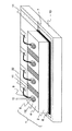
図5(A)と図5(B)に、本発明の第1の実施の形態における光半導体素子の構成を示す。図5(A)にはその光半導体素子1の斜視図を、図5(B)にはその断面図を示す。本実施形態では、背景技術の欄で説明した複数の受光部13を有する光半導体素子1において、さらに受光部13間の位置に、第1のpin半導体接合層12と接触することなく第2のpin半導体接合層22を配置した構造の光半導体素子1を示している。
(First embodiment)
FIG. 5A and FIG. 5B show the configuration of the optical semiconductor element in the first embodiment of the present invention. FIG. 5A is a perspective view of the
本実施形態の光半導体素子は上記のようにpin構造のものであるが、後述するように、本発明はpn構造の光半導体素子にも適用できる。ただ、公知のように、pn構造ではその半導体接合面における空乏層が十分でないため、p層とn層よりもドーピング濃度が低いi層(光吸収層)を入れることで、光吸収をより高める、動作電圧を下げる等の特性改善を図っている。特に、InGaAsをi層とするIII−V族多元結晶pinフォトダイオードは、1μm帯の広い通信波長域をカバーしているので、光通信で多用されている。この点を考慮して、以下に述べる本発明の各実施形態では、pin半導体接合層を配置した光半導体素子を例示して本発明を説明することとする。 Although the optical semiconductor element of this embodiment has a pin structure as described above, the present invention can also be applied to an optical semiconductor element of a pn structure as will be described later. However, as is well known, the depletion layer at the semiconductor junction surface is not sufficient in the pn structure. Therefore, by adding an i layer (light absorption layer) having a lower doping concentration than the p layer and the n layer, light absorption is further enhanced. Improvement of characteristics, such as lowering the operating voltage. In particular, III-V group multi-crystal pin photodiodes having InGaAs as an i layer cover a wide communication wavelength region of 1 μm band, and are therefore widely used in optical communication. In consideration of this point, in each embodiment of the present invention described below, the present invention will be described by exemplifying an optical semiconductor element provided with a pin semiconductor junction layer.
本実施形態では、各受光部13間に、上記のように第2のpin半導体接合層22を配置したことにより、クロストークを低減することが可能になる。その動作機構を以下に説明する。
In the present embodiment, crosstalk can be reduced by arranging the second pin
発明が解決しようとする課題の欄で述べたような、問題となるクロストークの大きく分けた2つの要因の内の一つ目である、受光すべき信号光が吸収層に完全に吸収されずにその信号光の一部はそのまま光半導体素子1の裏面に到達して再び反射散乱を繰り返しつつ受光を所望しない他のチャンネルの第1のpin半導体接合層領域12に達しようとする不要な漏れ光、もしくは反射散乱を繰り返す光の一部で、所定のチャンネル以外の吸収層領域においてキャリアを発生させ、そのまま拡散もしくはドリフトにより他のチャンネルの第1のpin半導体接合層12に達しようとする不要な漏れ光を、本発明により新たに配置した第2のpin半導体接合層22において吸収させることが可能となる。すなわち、本発明によれば、クロストークの原因となる不要な漏れ光を、入力を所望しない他のチャンネルの第1のpin半導体接合層12に到達する前に、第2のpin半導体接合層22において吸収できるため、従来技術の光半導体素子と比較して大幅にクロストークを低減することが可能となる。
As described in the section of the problem to be solved by the invention, the signal light to be received, which is one of the two major factors of the crosstalk in question, is not completely absorbed by the absorption layer. In addition, a part of the signal light reaches the back surface of the
第2のpin半導体接合層22は、従来の半導体製造プロセスにおいて、第1のpin半導体接合層12を形成する工程と同時に、形成することが可能である。すなわち、第1のpin半導体接合層12を構成するp型拡散領域5を形成するために使用するマスクデザインに、第2のpin半導体接合層22を構成するp型拡散領域を形成するためのマスクデザインを追加変更するだけで対応が可能となるため、本実施形態の実現においてはなんら従来の半導体製造プロセスに負担をかけることなく、つまり製造工程数の増加を招くことなく、その第2のpin半導体接合層22の実現が可能である。本発明の光半導体素子の作製は格別特殊な工法を必要とせず、従来の一般的な素子作製方法(非特許文献2)の応用で実現できるので、簡略のためその他の構成要素についての製造工程の詳細説明は省略する。
The second pin
また、図5(A)、図5(B)に示すような4つの受光部13を有する光半導体素子において、寸法例を挙げると、受光部間隔250μm、各受光径80μm、光吸収層3の厚さ3.6μmであり、光半導体素子外形寸法は縦1000μm、幅350μm、厚さ150μmである。さらに、本発明による、第2のpin半導体接合層の導入パタンは、図5においては、短径70μm、長径150μmの楕円形状である。ただし、これらの寸法は典型的な値であり、本発明はこれらの値に拘束されるものではない。
Further, in the optical semiconductor element having the four
また、本発明では、受光部13のピッチ間隔を広げることによりクロストークを抑制する必要がないので、受光部13のピッチ間隔を好ましい500μm以下とすることができる。
In the present invention, since it is not necessary to suppress crosstalk by increasing the pitch interval of the
以上、本発明の第1の実施形態で用いた構成要素は、本第1の実施形態に限定されるものではなく、後述の本発明の第2の実施形態以降の他の実施形態にも実施可能なものである。また、本明細書で開示したこれら本発明の実施形態の変形、代替等の適用は、本発明の主旨となるその効果を阻害することがない範囲において実施可能である。例えば、以下の通りである。 As described above, the components used in the first embodiment of the present invention are not limited to the first embodiment, and are also implemented in other embodiments after the second embodiment of the present invention described later. It is possible. In addition, modifications, substitutions, and the like of the embodiments of the present invention disclosed in the present specification can be implemented within a range that does not hinder the effect that is the gist of the present invention. For example, it is as follows.
第2のpin半導体接合層22の形状は、図5(A)に示したような楕円に限るものではなく、たとえば円形でもよいし、あるいは長方形でもよく、その形状を限定するものではない。特に、図6に示すように、隣接する受光部13間において、光半導体素子1の対向する端面から端面へ完全に光半導体素子1を横切るように第2のpin半導体接合層22を配置することにより、チャンネル間の分離を完全なものとすることができるため、クロストークの低減効果は大きいものとなる。
The shape of the second pin
また、第2のpin半導体接合層22の形成は、必ずしも第1のpin半導体接合層12と同時に形成しなければならないということではない。たとえば、第2のpin半導体接合層22におけるp型拡散領域5におけるドーピング濃度を、第1のpin半導体接合層12におけるp型拡散領域5よりも高くすることによって、第2のpin半導体接合層22の空乏層化を第1のpin半導体接合層12の空乏層化よりも際立たせることが可能となる。それにより、受光部13間における不要な漏れ光の吸収をより高めることとなり、その結果クロストーク低減効果をより高めることが可能となる。
Further, the formation of the second pin
また、PD(フォトダイオード)を形成する基板2にはInPに限らず、PD構造を形成できるのであれば、たとえばGaAs、Si、Ge、SiGe等の他の基板を用いてもよい。ドーピング材料としては、n型ドーピング材として、Si(シリコン)、Se(セレン)、S(硫黄)、Sn(錫)等が使用できる。一方、p型ドーピング材としては、Zn(亜鉛)、カドミウム(Cd)、ベリリウム(Be),マグネシウム(Mg)を用いることができる。
Further, the
また、基板2上の積層構成においても、図5、図6の例ではn型基板2上に光吸収層3とn型埋め込み層4を順次積層させ、さらにn型埋め込み層4の一部にp型拡散領域5を形成したが、その逆の積層構成でもよい。すなわち、p型基板上に光吸収層とp型埋め込み層を順次積層させ、さらにp型埋め込み層の一部にn型拡散領域を形成した積層構成でもよい。以上の構成は、一般に光吸収層にInGaAsやInGaAsPを用いて形成したヘテロ構造を成すpin半導体接合層を供するが、ホモ構造によるpin半導体接合層を用いてもよいし、受光が可能であればpin半導体接合層の代わりにpn接合層を用いてもよい。例えば、背景技術の欄でも説明したように、通信波長帯で主に使われるInGaAs/InGaAsPの混晶半導体においては、光の吸収が1.6μm帯以上の波長域で急激に落ちてくるため、この波長域においては光が吸収されにくい分、漏れ光成分となってクロストークが大きくなる。従って、1.2μm〜1.7μm帯の波長光を受光できるInGaAs/InGaAsPの混晶半導体を用いた光半導体素子に本発明を適用すれば、好ましいクロストーク改善効果が得られる。ただし、本発明は、pinもしくはpnの半導体接合層が構成できて受光機能があるものであれば、特にその波長を限定するものではない。
Also in the laminated structure on the
また、本実施形態では、受光部13の数を4個にした例を挙げたが、本発明はその数を限定するものではない。すなわち受光部13の数は、2個以上の複数個であればよい。また、複数の受光部13は、等間隔ピッチに配置されていてもよいし、不等間隔に任意のピッチに配置されていてもかまわない。
In the present embodiment, an example in which the number of the
本実施形態では、特にpin半導体接合層を用いて例示したが、上述したように本発明はこれに限定されない。すなわち、本発明を構成する半導体接合層としては、pin半導体接合層だけでなく、例えばpn半導体接合層でも、本発明のクロストーク低減効果が得られる。このpn半導体接合層の場合は、例えば、図5(B)に示す構造から符号3で示す光吸収層(i層)を取り除いた構造になる(図示しない)。ただし、pn構造よりは、pin構造による第2の半導体接合層22を配置する方が、i層(吸収層)を有する分だけ、本発明のクロストーク低減効果は大きい。従って、pn構造による第2の半導体接合層よりは、pin構造による第2の半導体接合層を配置した方がより望ましいといえる。このことは、後述の他の実施形態にも当てはまる。
In the present embodiment, the pin semiconductor junction layer is specifically exemplified, but the present invention is not limited to this as described above. That is, as the semiconductor junction layer constituting the present invention, not only the pin semiconductor junction layer but also, for example, a pn semiconductor junction layer, the crosstalk reduction effect of the present invention can be obtained. In the case of this pn semiconductor junction layer, for example, the structure shown in FIG. 5B is removed from the light absorption layer (i layer) indicated by reference numeral 3 (not shown). However, the arrangement of the second
(第2の実施形態)
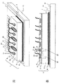
図7(A)と図7(B)に、本発明の第2の実施の形態における光半導体素子の構成を示す。図7(A)にはその光半導体素子の斜視図を、図7(B)にはその断面図をそれぞれ示す。本実施形態では、第1の実施形態と異なって、第1のpin半導体接合層12の周囲を完全に囲って、第2のpin半導体接合層22を配置した形態を示している。このように第2のpin半導体接合層22を配置することで、第1の実施形態にも増して、全方向から反射散乱する不要な漏れ光を吸収することが可能となる。
(Second Embodiment)
FIG. 7A and FIG. 7B show the configuration of the optical semiconductor element in the second embodiment of the present invention. 7A is a perspective view of the optical semiconductor element, and FIG. 7B is a cross-sectional view thereof. In the present embodiment, unlike the first embodiment, the second pin
さらに、本実施形態の構造は、以下に述べる効果を新たに生むという特徴がある。すなわち、作製プロセスのデザインルールが許す範囲であれば、図8(A)および図8(B)に示すように、第2のpin半導体接合層22をできるだけ第1のpin半導体接合層12に近づけ、また第1のpin半導体接合層12と接することなく素子の全域にわたって配置することで、受光部13面の上方からビームを広げつつ入射する光信号のうち、所望のチャンネルの受光部13に入射しきれなかった不要な漏れ光についても確実に吸収することができるようになるため、クロストークの低減効果をより一層高めることができる。
Furthermore, the structure of the present embodiment is characterized in that the following effects are newly produced. That is, as long as the design rules of the manufacturing process allow, as shown in FIGS. 8A and 8B, the second pin
さらに、従来の例示(図1(A)および図1(B))における光半導体素子1では、光半導体素子1の切り出し面(すなわち、劈開もしくはダイシングにより切り出された光半導体素子の側面)から、外部からの迷光が入射した場合、受光感度の劣化を招くといった問題があった。そのため、図2に示すように従来の半導体素子をモジュール化する際にも、これら迷光に対する遮光対策が必要であった。これに対し、本実施形態では、図7(A)または図8(A)に示すように、第1のpin半導体接合層12の周囲を完全に囲って第2のpin半導体接合層22を配置しているので、クロストークの原因となる受光部13間に侵入した不要な漏れ光を吸収するだけにとどまらず、加えて外部からの迷光も遮断することができるという新たな効果も生まれるため、光半導体素子1の受光特性を改善できるという効果も得ることができるようになる。
Furthermore, in the
さらに、図9に示すような、2次元に配置した受光部13を有する光半導体素子23の場合、隣接する受光部13からのクロストークは、1次元で配列されたアレイ型の光半導体素子1のそれと異なって、周囲360度にわたってその原因が存在することになる。図9に示すように、2次元に配置された光半導体素子23の場合には、第1のpin半導体接合層12の周囲を完全に囲うように第2のpin半導体接合層22を配置することによって、クロストークの低減効果は大きいものとなる。図9に示した光半導体素子23の受光部は、それら受光部の配置が等間隔ピッチである場合の例を示しているが、それら受光部が不等間隔に任意のピッチで配置されてもかまわない。尚、2次元に配置した受光部13を有する光半導体素子23を内蔵した光モジュールについては、後述の第8の実施形態8で言及する。
Furthermore, in the case of the
(第3の実施形態)
図10(A)と図10(B)に本発明の第3の実施の形態における光半導体素子の構成を示す。図10(A)にはその光半導体素子1の斜視図を、図10(B)にはその断面図を示す。本実施形態では、前述した第1の実施形態および第2の実施形態と異なって、受光部13への光入力を遮断することなく第1のpin半導体接合層12に接続された第1の電極8と、この第1の電極8とは絶縁を確保しつつ第2のpin半導体接合層22に接続された第2の電極24とが配置された形態を示している。第2の電極24は、その一部もしくは全体が、第2のpin半導体接合層22を構成するp型拡散領域5と接続される。図10(A)に示す第2の電極24は、第2のpin半導体接合層22を構成するp型拡散領域5の全体を覆う状態で配置された場合を例示している。さらに、第2の電極24の各々はボンディングワイヤ9を介して、外部の電気配線板10上に形成した電気配線11と接続されている。なお、図中、第2の電極24で覆われた第2のpin半導体接合層22を分かりやすく表示するために、第2の電極24を白抜き輪郭太線で描画している。
(Third embodiment)
FIG. 10A and FIG. 10B show the configuration of the optical semiconductor element in the third embodiment of the present invention. 10A is a perspective view of the
第2の電極24の接続先について、二通りの場合について述べる。まず、一つ目として、第2の電極24の接続先が、裏面電極7と共通化されて接続される場合、すなわちショート(短絡)接続された場合について述べる。第2の電極24がショート接続されると、第2のpin半導体接合層22における光吸収層内に発生する空乏層の状態は、第1の実施形態で述べた構成(第2の電極24をオープンにした場合も同じ)のそれよりも、電気的な揺らぎに影響されにくい状態になるので、不要な漏れ光をより安定して吸収することができ、クロストークの変動を抑えることが可能となる。
Regarding the connection destination of the
次に、第2の電極24の接続先と、裏面電極6との間で、第2のpin半導体接合層22に対して逆バイアス電圧を印加した場合について述べる。逆バイアス電圧が第2のpin半導体接合層22に印加されると、第2のpin半導体接合層22における光吸収層3内が完全に空乏層化する。その結果、受光感度が増すこととなる。このことが第2のpin半導体接合層22で生じることにより、上記のようにショート接続した場合と比較して、不要な漏れ光をより一層捕らえることが可能となる。
Next, a case where a reverse bias voltage is applied to the second pin
各々の第2の電極24に印加するバイアス電圧の値は、すべて同じ値でもよいし、各々が異なる値でもよい。そのバイアス電圧値を各々異なるように調整可能とすることで、例えば作製プロセスの制約のためにp型拡散領域の大きさが異なってしまうような場合などにおいて、印加電圧の値を各々の第2のpin半導体接合層22に対して個別に最適化することができる。
The values of the bias voltages applied to the respective
また、第2の電極24に印加するバイアス電圧の値を、第1の電極24に印加するバイアス電圧と同じ値にしてもよい。この場合は、電圧源が共通化できて、1つの電圧源ですむという利点がある。勿論、第2の電極24に印加するバイアス電圧値を、第1の電極24に印加するバイアス電圧値と異なるようにしてもかまわない。
Further, the value of the bias voltage applied to the
以上、第2の電極24の接続先について述べたが、いづれにしても従来技術に対してクロストークの低減効果は大きいものとなる。
Although the connection destination of the
第2の電極24は、従来の半導体製造プロセスにおいて、第1の電極8を形成する工程と同時に形成することが可能である。すなわち、第1の電極8を形成するために使用するマスクデザインに第2の電極24を形成するためのマスクデザインを追加変更するだけで対応が可能であるため、本実施形態の実現においてはなんら従来の半導体プロセスに負担をかけることなく、つまり製造工程数の増加を招くことなく、第2の電極24の実現が可能となる。
The
(第4の実施形態)
本発明の第3の実施形態で示したような第2のpin半導体接合層22に第2の電極24を接続して配置した形態では、各々の第2の電極24に対して外部と電気的接続を個別に確保しようとすると、各々の第2の電極24に対して、それぞれ個別のボンディングワイヤ9が必要となる。このことは、受光部13のピッチ間隔がより狭くなった場合、すなわち、受光部のピッチ間隔を狭めて、光半導体素子の小型化を目指すような場合には、第1の電極8と接続されたボンディングワイヤ9と第2の電極24と接続されたボンディングワイヤ9とが接触してショートしやすくなるといったおそれが生じてくる。また、光半導体素子に多数のボンディングワイヤ9を打つことは、光モジュールの組立工程を複雑なものにする。従って、第2のpin半導体接合層22と接続された第2の電極24へのボンディングワイヤの数は少ない程よいということが分かる。
(Fourth embodiment)
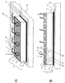
In the configuration in which the
そこで、本発明は第4の実施形態では、ボンディングワイヤの数をできるだけ少なくする形態について、図11、図12および図13を用いて説明する。本実施形態では、第2の電極24を共通化し、その単一の第2の電極24を第2のpin半導体接合層22を構成するp型拡散領域5の一部もしくは全体に接続した状態に配置している。なお、図11、図12および図13においては、第2の電極24と重なりつつ接続されている部分のp型拡散領域5を分かりやすく表示するために、第2の電極24を白抜き輪郭太線で描画している。
Therefore, in the fourth embodiment, an embodiment in which the number of bonding wires is reduced as much as possible will be described with reference to FIGS. 11, 12, and 13. In the present embodiment, the
図11に示す光半導体素子1では、第3の実施形態と異なって、それぞれの第2のpin半導体接合層22と接続された第2の電極24の各々が互いに電気的に連結接続して配置されている。このように第2の電極24を共通化、一体化することにより、第2の電極24に必要なボンディングワイヤ9は最低1本からで良くなるため、ボンディングワイヤの数が多いことから生ずる上述した不都合を回避できるという効果が生じる。
In the
また、図12に示す光半導体素子1では、第3の実施形態と異なって、第2のpin半導体接合層22の各々を互いに電気的に接続して一体化し、そのp型拡散領域5の一部に単一の第2の電極24を接続して配置している。このように第2のpin半導体接合層22を共通化、一体化することによっても、第2の電極24に必要なボンディングワイヤ9は最低1本からで良くなるため、ボンディングワイヤの数が多いことから生ずる上述した不都合を回避できるという効果が生じる。
Further, in the
さらに、図13に示す光半導体素子1では、第2の実施形態の図8(A)で示した効果に加え、最低1本からのボンディングワイヤで第3の実施形態で述べた効果を生じることが可能となるため、より一層の不要な漏れ光の吸収が可能となる。
Furthermore, in the
前述した他の実施形態と同様に、本実施形態においても、光半導体素子1の作製プロセスにおいて、第1の電極8を形成するために使用するマスクデザインに第2の電極24を形成するためのマスクデザインを追加変更する、あるいはp型拡散領域5を形成するために使用するマスクデザインを追加変更するだけで本実施形態の実現への対応が可能となるため、本実施形態の実現においてはなんら従来の半導体プロセスに負担をかけることなく、つまり製造工程数の増加を招くことなく、本実施形態のの実現が可能であるという特徴を有する。
Similar to the other embodiments described above, also in this embodiment, in the manufacturing process of the
(第5の実施形態)
図14(A)と図14(B)に本発明の第5の実施の形態の光半導体素子の構成を示す。図14(A)にはその光半導体素子1の斜視図を、図14(B)にはその断面図を示す。本実施形態では、上記の第4の実施形態で説明した図13の構成と異なって、受光部13への光入力を遮断することなく、第1のpin半導体接合層12と接続された第1電極8とは絶縁を確保しつつ、第2のpin半導体接合層22に接続された第2の電極24を光半導体素子1の表面全体を覆って配置した形態を示している。なお、図中、第2の電極24で覆われた第2のpin半導体接合層22を分かりやすく表示するために、第2の電極24を白抜き輪郭太線で描画している。このような形態を実施することにより、第2の実施形態の図8(A)で示した構成により生じる効果に加え、最低1本からのボンディングワイヤで良いので第3の実施形態で述べた効果を生じることが可能となる。
(Fifth embodiment)
FIGS. 14A and 14B show the configuration of an optical semiconductor element according to the fifth embodiment of the present invention. FIG. 14A is a perspective view of the
さらに、本実施形態によれば、それ以上に根本的な特性改善を期待することが可能となる。すなわち、光半導体素子1の表面全体を覆って配置した第2の電極24の存在そのものにより、発明が解決しようとする課題の欄で述べたように、問題となるクロストークの大きく二つの要因の内の二つ目の解決すべき課題をほぼ取り去ることが可能となる。従来の技術を示す図4に示したように、光導波路20の端に図2の従来の光モジュール14を実装した場合には、光導波路20から出射した光信号は、その間隙を伝わる間にもそのビーム幅を広げるため、光入力を所望するチャンネルの受光部13以外の領域にも光信号の一部が侵入しまうことは既に述べた通りである。しかし、本実施形態のように、光半導体素子1の表面全体を覆って配置した第2の電極24の存在そのものにより、所望する受光部13において吸収されることがないであろう不要となる一部の光信号ついては、その侵入前に反射させてしまうため、不要な漏れ光の発生そのものを遮断できるという、極めてクロストークの削減効果の大きい効果を生む。加えて、本実施形態では、第1のpin半導体接合層12の周囲を完全に囲って第2のpin半導体接合層22を配置した形態を有しているので、光半導体素子1周辺から漏れ込む迷光に対しても、さらには一部発生した漏れ光についても十分な吸収ができる作用が得られる。さらに、第2の電極24を介して逆バイアス電圧を印加することにより、クロストークの削減効果を最大限に引き出すことが可能となる。
Furthermore, according to the present embodiment, it is possible to expect a fundamental improvement in characteristics. That is, the existence of the
本実施形態によるクロストーク改善効果について具体的な測定結果例を挙げてさらに説明する。まず、図1(A),(B)に示した従来技術による隣接クロストークは、−26.7dB@1550nm、−25.6dB@1610nmであった。これに対し、図14(A)、(B)に示した本発明の第5の実施形態による隣接クロストークは、−36.9dB@1550nm、−34.5dB@1610nmであった。すなわち、本実施形態によれば、少なくとも、1550nmにおいて10.2dB以上、1610nmにおいて8.9dB以上のクロストーク改善効果があることが分かった。また、低い環境温度におけるクロストークとしては、−5度において、1610nmにおいても−33.2dBとなり、−26dB以上を十分に満足するクロストーク特性の改善を実現することができた。 The crosstalk improvement effect according to the present embodiment will be further described with specific measurement result examples. First, the adjacent crosstalk according to the prior art shown in FIGS. 1A and 1B was −26.7 dB @ 1550 nm and −25.6 dB @ 1610 nm. On the other hand, the adjacent crosstalk according to the fifth embodiment of the present invention shown in FIGS. 14A and 14B was −36.9 dB @ 1550 nm and −34.5 dB @ 1610 nm. That is, according to the present embodiment, it was found that there was at least a crosstalk improving effect of 10.2 dB or more at 1550 nm and 8.9 dB or more at 1610 nm. Further, the crosstalk at a low ambient temperature was −33.2 dB at −5 degrees and also at 1610 nm, and an improvement in crosstalk characteristics sufficiently satisfying −26 dB or more could be realized.
(第6の実施形態)
図15に示す光モジュールは、背景技術の欄でも説明した光モジュール同様に、筺体15の内部に、上述してきた各実施形態において作製した光半導体素子1の一つを実装した場合の一例を示す。図15では、第5の実施形態で説明した光半導体素子1を実装した例を示す。本発明による上述のようなクロストークの低減構造を有する光半導体素子1を使用することにより、光モジュールのクロストーク特性も改善できるようになる。
(Sixth embodiment)
The optical module shown in FIG. 15 shows an example in which one of the
第2の電極24を有する光半導体素子を実装した場合でも、その第2の電極24から電気的接続を筺体15外部に取り出すために形成した筐体側の電気配線18は、他の電気配線18と同時に形成することが可能であるため、なんら従来の筐体15の製造構成において負担をかけることなく、つまり製造工程数の増加を招くことなく、その光モジュールの実現が可能である。
Even when the optical semiconductor element having the
図15のモジュールの形態として、寸法例を挙げると、セラミック筐体15の寸法は縦6500μm、幅2500μm、厚さ1000μmであり、窓蓋16の寸法は縦6500μm、幅2500μm、厚さ200μmである。ただし、これらの寸法は参考のために例示した典型的な値であり、本発明はこれらに拘束されるものではないことは勿論である。
As an example of the dimensions of the module shown in FIG. 15, the
(第7の実施形態)
図16に示す光モジュールは、第6の実施形態で説明した光モジュールにさらに実用性を備えさせた場合の一例を本発明の第7の実施形態として示す。本光モジュール14は背景技術の欄でも説明した図3の構成と同様に、筐体15内部に、上述した第6の実施形態において作製したクロストークの低減構造を有した光半導体素子1を実装している。図16の構成では、筐体15に取り付けられたリードピン21を介して筐体外部に電極を取り出すことができるようになっている。また、8つの受光部(ここでは図示しない)を有する光半導体素子1を内蔵した光モジュール14に8芯の光ファイバアレイ25を取り付けている。
(Seventh embodiment)
The optical module shown in FIG. 16 shows an example where the optical module described in the sixth embodiment is further provided with practicality as the seventh embodiment of the present invention. In the present
一方、発明が解決しようとする課題の欄で述べたクロストーク要因を抱えた従来技術で生産された光半導体素子を用いて、図16に示すような光モジュールを作製した場合、以下に述べる理由で、その製造コストが高止まりしていた。すなわち、受光部のピッチ間隔が通常使用される光ファイバアレイのファイバ整列ピッチ間隔の250μmの場合であっても、仕様によっては十分にクロストーク特性を満足することが困難な場合もあった。これは、特に光通信波長で長波長側であるL帯の波長域にある光信号では、空間に出射された後のビームの広がりが大きいため、発明が解決しようとする課題の欄で述べたように、問題となるクロストーク要因の内の二つ目の課題の影響を大きく受けていたためである。さらに、低温環境における光半導体素子の受光特性が低下するという物理的特性から、クロストーク要因の内の一つ目の課題の影響を大きく受けていた。そこで、従来技術で製造された光半導体素子の受光部はそのピッチ間隔をできるだけ離して、具体的には500μm以上のピッチ間隔を採用することで、クロストークの低減を図っていた。しかし、受光部のピッチ間隔の拡大は、光半導体素子そのものの形状を大型化することなる。このことは、光半導体素子を所定のアレイ数で切り出す際には、その工程自体を困難なものとしたり、あるいは素子そのものの取り扱いを困難にするという問題を生じさせていた。また大型化により1枚のウェハから切り出せる光半導体素子の収穫数が少なくなり、コスト高を招く原因ともなっていた。一方で、規格外の500μm以上の光ファイバアレイの調達を必要とするなど、光モジュールの製造についても更なるコスト高を招いていた。 On the other hand, when an optical module as shown in FIG. 16 is manufactured using the optical semiconductor element produced by the prior art having the crosstalk factor described in the section of the problem to be solved by the invention, the reason described below The production cost was still high. That is, even if the pitch interval of the light receiving portions is 250 μm, which is the fiber alignment pitch interval of the optical fiber array that is normally used, it may be difficult to sufficiently satisfy the crosstalk characteristics depending on the specifications. This is described in the section of the problem to be solved by the invention because the optical signal in the L-band wavelength region, which is the longer wavelength side of the optical communication wavelength, has a large beam spread after being emitted into space. This is because it was greatly influenced by the second problem among the crosstalk factors in question. Furthermore, due to the physical characteristic that the light receiving characteristic of the optical semiconductor element deteriorates in a low temperature environment, it was greatly influenced by the first problem among the crosstalk factors. In view of this, the light receiving portions of the optical semiconductor element manufactured by the conventional technique are designed to reduce the crosstalk by separating the pitch intervals as much as possible, specifically adopting a pitch interval of 500 μm or more. However, the increase in the pitch interval of the light receiving parts increases the size of the optical semiconductor element itself. This causes a problem that when the optical semiconductor element is cut out with a predetermined number of arrays, the process itself becomes difficult, or the handling of the element itself becomes difficult. Further, the increase in size has resulted in a decrease in the number of harvested optical semiconductor elements that can be cut out from a single wafer, which has been a cause of increased costs. On the other hand, the cost of manufacturing optical modules has been further increased, such as the need to procure optical fiber arrays of 500 μm or more that are out of specification.
しかし、これまでの本発明の各実施形態で述べてきた第2のpin半導体接合層22を配置した光半導体素子1においては、一層のクロストーク低減効果が得られるので、受光部13のピッチ間隔を狭めることが可能となる。例えば、通常一般に使用される光ファイバアレイ25のファイバ整列ピッチ間隔は、250μmもしくは127μmのものがある。本実施形態では、これらの光ファイバアレイ25を用いた様子を図16に示している。これら各々の光ファイバと光学的な結合を得るために、光半導体素子1の受光部のピッチ間隔も250μmもしくは127μmに配置して作製してある。このように通常入手しやすい規格に沿った光ファイバアレイ25を光モジュールに適用できることは、部材の調達コストを大幅に低減できるという効果を生む。
However, in the
尚、云うまでもないが、光半導体素子1の受光部のピッチ間隔は、250μmもしくは127μmが最適であるというわけではなく、その受光部のピッチ間隔についてはなんら制限を与えるものではなく、そのピッチ間隔は任意に採用可能である。むしろ本発明の光半導体素子1を使用することにより、クロストークの削減効果が得られる分だけ素子サイズを小型化でき、ひいては光モジュールを小型化できるという効果が得られる点に注目すべきである。
Needless to say, the optimum pitch interval of the light receiving portions of the
(第8の実施形態)
図17と図18に本発明の第9の実施の形態における光モジュールの構成を示す。図17にはその光モジュールの斜視図を、図18にはその断面図を示す。本実施形態では、第2の実施形態で述べた2次元に配列された受光部13を有する光半導体素子23(図9)を、筐体15内に内蔵し、さらにPLC(Planar Lightwave Circuit)19上に表面実装した光モジュールについて説明する。ここで光半導体素子23は、筐体15側に固定しているのではなく、受光部13を窓蓋16側に対向させた状態で直接窓蓋16上に形成した電極26に対してフリップチップ実装しており、これによって電極を取り出している。このように構成したのは、2次元に配列された受光部13を遮蔽することなく、多数の第1の電極8及び第2の電極24からボンディングワイヤにより電極を取り出すことが非常に困難であるからである。本実施形態では、第1の電極8及び第2の電極24は窓蓋側の電極と金属半田7等により接続され、裏面電極6がボンディングワイヤ9によって接続されている。筐体15からの電極の取り出しは、例えばFPC(Flexible Printed Circuit)27等を用いることにより可能である。PLC19側においては、光導波路20の端に反射ミラー28が形成されている。光導波路20を伝播してきた光信号は、この反射ミラー28により反射されて上部に対面して設置された受光部13へ入射する構成となっている(図中、破線矢印)。
(Eighth embodiment)
17 and 18 show the configuration of the optical module according to the ninth embodiment of the present invention. FIG. 17 is a perspective view of the optical module, and FIG. 18 is a sectional view thereof. In the present embodiment, the optical semiconductor element 23 (FIG. 9) having the
上記のような配置構成にすることで、第2のpin半導体接合層22を配置した光半導体素子23において受光部13を2次元に配列させた場合においても、クロストークの低減効果が期待できる光モジュールを提供することが可能である。
By adopting the arrangement configuration as described above, even when the
(第9の実施形態)
以上の実施形態で述べてきた光半導体素子におけるPDの構成は、いずれも基板に対して上面から光信号を入射させる面入射型PDの構成であったが、本発明における第2のpin半導体接合層22を配置できるのは、このPD構成に限定されるものではない。すなわち、光信号の入射位置が確保できるのであれば、基板の裏面から光信号を入射させる裏面入射型PDの構成であってもよい。また、基板に対して水平方向から光信号を入射させる端面入射型の導波路型PDの構成であってもよいし、屈折型PDであってもよい。また、アバランシェPDやUTC−PD(単一走行キャリアPD)においても、本発明の効果を同様に得ることが可能である。
(Ninth embodiment)
The PD configuration in the optical semiconductor element described in the above embodiments is a configuration of a surface incidence type PD in which an optical signal is incident on the substrate from the upper surface. However, the second pin semiconductor junction in the present invention is used. The arrangement of
以上述べてきた本発明の構成は、光半導体によるPDの種類のいかんに拘わることなく、本来の信号光を受光すべき受光部(第1の半導体接合部)の他に、これら受光部間において、第2の半導体接合部を設けることが可能であれば、クロストークの低減を図ることが可能となる。すなわち、PDの構成にはなんら制限されない。 The configuration of the present invention described above is not limited to the type of PD using an optical semiconductor, but between the light receiving portions in addition to the light receiving portion (first semiconductor junction portion) that should receive the original signal light. If the second semiconductor junction can be provided, crosstalk can be reduced. That is, the configuration of the PD is not limited at all.
さらに、以上の実施形態で述べてきた光半導体素子の電極の配置は、第1の電極もしくは第2の電極が裏面電極に対して基板の別の面、すなわち基板の表と裏に配置されている構成であったが、このことについても、本発明においてはその構成に限定されるものではない。すなわち、本発明における第2のpin半導体接合層を配置できるデザインであれば、第1の電極もしくは第2の電極と同じ基板面に裏面電極と同じ機能を有する電極を形成してもよい。つまり、すべての電極を、基板の片面に形成してもよい。 Furthermore, the arrangement of the electrodes of the optical semiconductor element described in the above embodiment is such that the first electrode or the second electrode is arranged on another surface of the substrate with respect to the back electrode, that is, on the front and back of the substrate. However, the present invention is not limited to this configuration. That is, an electrode having the same function as the back electrode may be formed on the same substrate surface as the first electrode or the second electrode as long as the second pin semiconductor junction layer in the present invention can be arranged. That is, all the electrodes may be formed on one side of the substrate.
以上論述したように、本発明において実施できる光半導体素子の形態は、複数の受光部を有する光半導体素子において、受光部間において第1のpin半導体接合層と接触することなく第2のpin半導体接合層を配置した光半導体素子を配置するだけで、そのPD構成に関わらずクロストークの低減効果を得ることが可能である。 As described above, the form of the optical semiconductor element that can be implemented in the present invention is an optical semiconductor element having a plurality of light receiving parts, in which the second pin semiconductor is not in contact with the first pin semiconductor junction layer between the light receiving parts. By merely disposing an optical semiconductor element having a bonding layer, it is possible to obtain a crosstalk reduction effect regardless of the PD configuration.
(他の実施の形態)
上記では、本発明の好適な実施形態を例示して説明したが、本発明の実施形態は上記例示に限定されるものではなく、特許請求の範囲に記載の範囲内であれば、その構成部材等の置換、変更、追加、個数の増減、形状の設計変更等の各種変形は、全て本発明の実施形態に含まれる。
(Other embodiments)
In the above, the preferred embodiment of the present invention has been described by way of example. However, the embodiment of the present invention is not limited to the above-described example, and the constituent members thereof are within the scope of the claims. Various modifications such as replacement, change, addition, increase / decrease in number, change in shape design, and the like are all included in the embodiment of the present invention.
例えば、上述した本発明の各実施形態では、特にpin半導体接合層を用いて例示したが、本発明はこれに限定されない。すなわち、本発明を構成する半導体接合層としては、pin半導体接合層だけでなく、pn半導体接合層や、多層の半導体接合層を有するアバランシェPDやUTC−PD(単一走行キャリアPD)等においても適用可能であることはいうまでもない。例えば、pn半導体接合層を有する場合においても、pin半導体接合層を用いて説明した第1から第9までの実施形態に記載の全ての形態は、i層(光吸収層)が存在しないという違いだけで、同様に実施可能である。 For example, in each of the above-described embodiments of the present invention, the pin semiconductor junction layer is specifically exemplified. However, the present invention is not limited to this. That is, as a semiconductor junction layer constituting the present invention, not only a pin semiconductor junction layer but also a pn semiconductor junction layer, an avalanche PD having a multi-layer semiconductor junction layer, UTC-PD (single traveling carrier PD), etc. Needless to say, this is applicable. For example, even in the case of having a pn semiconductor junction layer, all the forms described in the first to ninth embodiments described using the pin semiconductor junction layer are different in that there is no i layer (light absorption layer). Can be implemented as well.
1 (1次元に受光部を有する)光半導体素子
2 (n型InP)基板
3 光吸収層
4 n型埋め込み層
5 p型拡散領域
6 裏面電極
7 (光半導体素子を固定する)金属半田
8 第1の電極
9 ボンディングワイヤ
10 電気配線板
11 (電気配線板上の)電気配線
12 第1のpin半導体接合層
13 受光部
14 (光半導体素子を内蔵する)光モジュール
15 筐体
16 窓蓋
17 (筺体と窓蓋を接合する)金属半田
18 (筐体の)電気配線
19 PLC
20 光導波路
21 リードピン
22 第2のpin半導体接合層
23 (2次元に受光部を有する)光半導体素子
24 第2の電極
25 光ファイバアレイ
26 (窓蓋側の)電極
27 FPC
28 反射ミラー
DESCRIPTION OF
DESCRIPTION OF
28 reflection mirror
Claims (11)
各前記受光部間において前記第1の半導体接合層と接触することなく第2の半導体接合層が配置されていることを特徴とする光半導体素子。 In an optical semiconductor element provided with a plurality of light receiving portions composed of a first semiconductor bonding layer for receiving an optical signal,
An optical semiconductor element, wherein a second semiconductor junction layer is disposed between each of the light receiving portions without contacting the first semiconductor junction layer.
前記第1の電極に対して絶縁を確保しつつ前記第2の半導体接合層に接続されている第2の電極と
を有することを特徴とする請求項1または2に記載の光半導体素子。 A first electrode connected to the first semiconductor junction layer without blocking light input to the light receiving unit;
The optical semiconductor element according to claim 1, further comprising: a second electrode connected to the second semiconductor bonding layer while ensuring insulation with respect to the first electrode.
An optical module comprising the optical semiconductor element according to any one of claims 1 to 10.
Priority Applications (1)
| Application Number | Priority Date | Filing Date | Title |
|---|---|---|---|
| JP2006088471A JP2007266251A (en) | 2006-03-28 | 2006-03-28 | Optical semiconductor device |
Applications Claiming Priority (1)
| Application Number | Priority Date | Filing Date | Title |
|---|---|---|---|
| JP2006088471A JP2007266251A (en) | 2006-03-28 | 2006-03-28 | Optical semiconductor device |
Publications (1)
| Publication Number | Publication Date |
|---|---|
| JP2007266251A true JP2007266251A (en) | 2007-10-11 |
Family
ID=38638956
Family Applications (1)
| Application Number | Title | Priority Date | Filing Date |
|---|---|---|---|
| JP2006088471A Pending JP2007266251A (en) | 2006-03-28 | 2006-03-28 | Optical semiconductor device |
Country Status (1)
| Country | Link |
|---|---|
| JP (1) | JP2007266251A (en) |
Cited By (7)
| Publication number | Priority date | Publication date | Assignee | Title |
|---|---|---|---|---|
| CN102623544A (en) * | 2011-01-27 | 2012-08-01 | Ntt电子股份有限公司 | Optical semiconductor device |
| JP2018125538A (en) * | 2018-02-20 | 2018-08-09 | ソニー株式会社 | Light receiving element, imaging element, and imaging apparatus |
| WO2020121851A1 (en) * | 2018-12-12 | 2020-06-18 | 浜松ホトニクス株式会社 | Light detection device |
| CN113167637A (en) * | 2018-12-12 | 2021-07-23 | 浜松光子学株式会社 | Optical detection device |
| US11296245B2 (en) | 2014-02-07 | 2022-04-05 | Sony Corporation | Image capturing apparatus including a compound semiconductor layer |
| US11513002B2 (en) | 2018-12-12 | 2022-11-29 | Hamamatsu Photonics K.K. | Light detection device having temperature compensated gain in avalanche photodiode |
| US11901379B2 (en) | 2018-12-12 | 2024-02-13 | Hamamatsu Photonics K.K. | Photodetector |
-
2006
- 2006-03-28 JP JP2006088471A patent/JP2007266251A/en active Pending
Cited By (14)
| Publication number | Priority date | Publication date | Assignee | Title |
|---|---|---|---|---|
| JP2012156391A (en) * | 2011-01-27 | 2012-08-16 | Nippon Telegr & Teleph Corp <Ntt> | Optical semiconductor device |
| US8704322B2 (en) | 2011-01-27 | 2014-04-22 | Nippon Telegraph And Telephone Corporation | Optical semiconductor device |
| US8916946B2 (en) | 2011-01-27 | 2014-12-23 | Nippon Telegraph And Telephone Corporation | Optical semiconductor device |
| CN102623544B (en) * | 2011-01-27 | 2015-05-20 | Ntt电子股份有限公司 | Optical semiconductor device |
| CN102623544A (en) * | 2011-01-27 | 2012-08-01 | Ntt电子股份有限公司 | Optical semiconductor device |
| US11296245B2 (en) | 2014-02-07 | 2022-04-05 | Sony Corporation | Image capturing apparatus including a compound semiconductor layer |
| JP2018125538A (en) * | 2018-02-20 | 2018-08-09 | ソニー株式会社 | Light receiving element, imaging element, and imaging apparatus |
| WO2020121851A1 (en) * | 2018-12-12 | 2020-06-18 | 浜松ホトニクス株式会社 | Light detection device |
| CN113167637A (en) * | 2018-12-12 | 2021-07-23 | 浜松光子学株式会社 | Optical detection device |
| US11513002B2 (en) | 2018-12-12 | 2022-11-29 | Hamamatsu Photonics K.K. | Light detection device having temperature compensated gain in avalanche photodiode |
| US11561131B2 (en) | 2018-12-12 | 2023-01-24 | Hamamatsu Photonics K.K. | Determination method and light detection device |
| US11901379B2 (en) | 2018-12-12 | 2024-02-13 | Hamamatsu Photonics K.K. | Photodetector |
| US11927478B2 (en) | 2018-12-12 | 2024-03-12 | Hamamatsu Photonics K.K. | Light detection device |
| JP7454917B2 (en) | 2018-12-12 | 2024-03-25 | 浜松ホトニクス株式会社 | light detection device |
Similar Documents
| Publication | Publication Date | Title |
|---|---|---|
| US10444451B2 (en) | Shielded photonic integrated circuit | |
| JP4859677B2 (en) | Photovoltaic module fabrication system and method | |
| US8183656B2 (en) | Photodiode | |
| JP2007266251A (en) | Optical semiconductor device | |
| US9219184B2 (en) | Avalanche photodiodes with defect-assisted silicon absorption regions | |
| KR100484998B1 (en) | Bidirectional optical transmission device | |
| WO2006025523A1 (en) | Photoelectric composite module | |
| US8907266B2 (en) | Light-receiving device array, optical receiver module, and optical transceiver | |
| JP5477148B2 (en) | Semiconductor optical wiring device | |
| CN117043948A (en) | LED chip-to-chip vertical emission optical communication with optical fibers | |
| JP2003249675A (en) | Light receiving element array | |
| JP4828103B2 (en) | Optical transceiver module | |
| JP4412105B2 (en) | Optical waveguide device | |
| JP4995867B2 (en) | Light emitting device and optical coupling module | |
| JP2014165224A (en) | Optical semiconductor device and optical semiconductor device manufacturing method | |
| JP2006053472A (en) | Optical waveguide module and optical information processing apparatus | |
| JP2009075465A (en) | Optical transception module | |
| JP2018098399A (en) | Semiconductor photodetector | |
| EP3171464A1 (en) | Apparatus for damping and monitoring emissions from light emitting devices | |
| JP2009026826A (en) | Optical transmitting and receiving module | |
| WO2020255936A1 (en) | Light reception element and light shielding structure for optical circuit | |
| KR100440431B1 (en) | opto-electronic submount for photo electric modules | |
| JP2006344681A (en) | Light receiving element and module thereof | |
| WO2023248369A1 (en) | Photodetector | |
| JP2006013048A (en) | Light emitting optical semiconductor element and light receiving optical semiconductor element |
Legal Events
| Date | Code | Title | Description |
|---|---|---|---|
| A521 | Request for written amendment filed |
Free format text: JAPANESE INTERMEDIATE CODE: A523 Effective date: 20070821 |
|
| A131 | Notification of reasons for refusal |
Free format text: JAPANESE INTERMEDIATE CODE: A131 Effective date: 20091106 |
|
| A02 | Decision of refusal |
Free format text: JAPANESE INTERMEDIATE CODE: A02 Effective date: 20100302 |