EP3171464A1 - Apparatus for damping and monitoring emissions from light emitting devices - Google Patents
Apparatus for damping and monitoring emissions from light emitting devices Download PDFInfo
- Publication number
- EP3171464A1 EP3171464A1 EP15195655.4A EP15195655A EP3171464A1 EP 3171464 A1 EP3171464 A1 EP 3171464A1 EP 15195655 A EP15195655 A EP 15195655A EP 3171464 A1 EP3171464 A1 EP 3171464A1
- Authority
- EP
- European Patent Office
- Prior art keywords
- electrodes
- damping
- light emitting
- substrate
- damping layer
- Prior art date
- Legal status (The legal status is an assumption and is not a legal conclusion. Google has not performed a legal analysis and makes no representation as to the accuracy of the status listed.)
- Withdrawn
Links
- 238000013016 damping Methods 0.000 title claims abstract description 202
- 238000012544 monitoring process Methods 0.000 title claims abstract description 41
- 239000000758 substrate Substances 0.000 claims abstract description 141
- 239000011521 glass Substances 0.000 claims abstract description 54
- 238000010521 absorption reaction Methods 0.000 claims abstract description 20
- 229920000642 polymer Polymers 0.000 claims abstract description 11
- 229910021417 amorphous silicon Inorganic materials 0.000 claims description 15
- 230000002093 peripheral effect Effects 0.000 claims description 6
- AMGQUBHHOARCQH-UHFFFAOYSA-N indium;oxotin Chemical compound [In].[Sn]=O AMGQUBHHOARCQH-UHFFFAOYSA-N 0.000 claims description 3
- 230000003247 decreasing effect Effects 0.000 claims 2
- 230000003287 optical effect Effects 0.000 description 48
- XUIMIQQOPSSXEZ-UHFFFAOYSA-N Silicon Chemical compound [Si] XUIMIQQOPSSXEZ-UHFFFAOYSA-N 0.000 description 7
- 229910052710 silicon Inorganic materials 0.000 description 7
- 239000010703 silicon Substances 0.000 description 7
- 239000013307 optical fiber Substances 0.000 description 6
- 238000001465 metallisation Methods 0.000 description 5
- 238000004519 manufacturing process Methods 0.000 description 4
- 239000002800 charge carrier Substances 0.000 description 3
- 239000013078 crystal Substances 0.000 description 3
- 231100000040 eye damage Toxicity 0.000 description 3
- 239000000615 nonconductor Substances 0.000 description 3
- 230000001902 propagating effect Effects 0.000 description 3
- 230000005540 biological transmission Effects 0.000 description 2
- 238000004891 communication Methods 0.000 description 2
- 238000000151 deposition Methods 0.000 description 2
- 230000008021 deposition Effects 0.000 description 2
- 230000000694 effects Effects 0.000 description 2
- 238000000034 method Methods 0.000 description 2
- 230000005855 radiation Effects 0.000 description 2
- 230000032683 aging Effects 0.000 description 1
- 230000033228 biological regulation Effects 0.000 description 1
- 230000001419 dependent effect Effects 0.000 description 1
- 239000000835 fiber Substances 0.000 description 1
- 239000000463 material Substances 0.000 description 1
- 238000005259 measurement Methods 0.000 description 1
- KKFHAJHLJHVUDM-UHFFFAOYSA-N n-vinylcarbazole Chemical compound C1=CC=C2N(C=C)C3=CC=CC=C3C2=C1 KKFHAJHLJHVUDM-UHFFFAOYSA-N 0.000 description 1
- 229920002382 photo conductive polymer Polymers 0.000 description 1
- 238000012545 processing Methods 0.000 description 1
- 238000001552 radio frequency sputter deposition Methods 0.000 description 1
- 238000002834 transmittance Methods 0.000 description 1
Images


Classifications
-
- H—ELECTRICITY
- H01—ELECTRIC ELEMENTS
- H01S—DEVICES USING THE PROCESS OF LIGHT AMPLIFICATION BY STIMULATED EMISSION OF RADIATION [LASER] TO AMPLIFY OR GENERATE LIGHT; DEVICES USING STIMULATED EMISSION OF ELECTROMAGNETIC RADIATION IN WAVE RANGES OTHER THAN OPTICAL
- H01S5/00—Semiconductor lasers
- H01S5/02—Structural details or components not essential to laser action
- H01S5/026—Monolithically integrated components, e.g. waveguides, monitoring photo-detectors, drivers
-
- H—ELECTRICITY
- H01—ELECTRIC ELEMENTS
- H01L—SEMICONDUCTOR DEVICES NOT COVERED BY CLASS H10
- H01L31/00—Semiconductor devices sensitive to infrared radiation, light, electromagnetic radiation of shorter wavelength or corpuscular radiation and specially adapted either for the conversion of the energy of such radiation into electrical energy or for the control of electrical energy by such radiation; Processes or apparatus specially adapted for the manufacture or treatment thereof or of parts thereof; Details thereof
- H01L31/08—Semiconductor devices sensitive to infrared radiation, light, electromagnetic radiation of shorter wavelength or corpuscular radiation and specially adapted either for the conversion of the energy of such radiation into electrical energy or for the control of electrical energy by such radiation; Processes or apparatus specially adapted for the manufacture or treatment thereof or of parts thereof; Details thereof in which radiation controls flow of current through the device, e.g. photoresistors
- H01L31/09—Devices sensitive to infrared, visible or ultraviolet radiation
- H01L31/095—Devices sensitive to infrared, visible or ultraviolet radiation comprising amorphous semiconductors
-
- H—ELECTRICITY
- H01—ELECTRIC ELEMENTS
- H01L—SEMICONDUCTOR DEVICES NOT COVERED BY CLASS H10
- H01L31/00—Semiconductor devices sensitive to infrared radiation, light, electromagnetic radiation of shorter wavelength or corpuscular radiation and specially adapted either for the conversion of the energy of such radiation into electrical energy or for the control of electrical energy by such radiation; Processes or apparatus specially adapted for the manufacture or treatment thereof or of parts thereof; Details thereof
- H01L31/12—Semiconductor devices sensitive to infrared radiation, light, electromagnetic radiation of shorter wavelength or corpuscular radiation and specially adapted either for the conversion of the energy of such radiation into electrical energy or for the control of electrical energy by such radiation; Processes or apparatus specially adapted for the manufacture or treatment thereof or of parts thereof; Details thereof structurally associated with, e.g. formed in or on a common substrate with, one or more electric light sources, e.g. electroluminescent light sources, and electrically or optically coupled thereto
- H01L31/16—Semiconductor devices sensitive to infrared radiation, light, electromagnetic radiation of shorter wavelength or corpuscular radiation and specially adapted either for the conversion of the energy of such radiation into electrical energy or for the control of electrical energy by such radiation; Processes or apparatus specially adapted for the manufacture or treatment thereof or of parts thereof; Details thereof structurally associated with, e.g. formed in or on a common substrate with, one or more electric light sources, e.g. electroluminescent light sources, and electrically or optically coupled thereto the semiconductor device sensitive to radiation being controlled by the light source or sources
- H01L31/161—Semiconductor device sensitive to radiation without a potential-jump or surface barrier, e.g. photoresistors
- H01L31/162—Semiconductor device sensitive to radiation without a potential-jump or surface barrier, e.g. photoresistors the light source being a semiconductor device with at least one potential-jump barrier or surface barrier, e.g. a light emitting diode
-
- H—ELECTRICITY
- H01—ELECTRIC ELEMENTS
- H01S—DEVICES USING THE PROCESS OF LIGHT AMPLIFICATION BY STIMULATED EMISSION OF RADIATION [LASER] TO AMPLIFY OR GENERATE LIGHT; DEVICES USING STIMULATED EMISSION OF ELECTROMAGNETIC RADIATION IN WAVE RANGES OTHER THAN OPTICAL
- H01S5/00—Semiconductor lasers
- H01S5/02—Structural details or components not essential to laser action
- H01S5/022—Mountings; Housings
- H01S5/0225—Out-coupling of light
- H01S5/02257—Out-coupling of light using windows, e.g. specially adapted for back-reflecting light to a detector inside the housing
-
- H—ELECTRICITY
- H01—ELECTRIC ELEMENTS
- H01S—DEVICES USING THE PROCESS OF LIGHT AMPLIFICATION BY STIMULATED EMISSION OF RADIATION [LASER] TO AMPLIFY OR GENERATE LIGHT; DEVICES USING STIMULATED EMISSION OF ELECTROMAGNETIC RADIATION IN WAVE RANGES OTHER THAN OPTICAL
- H01S5/00—Semiconductor lasers
- H01S5/02—Structural details or components not essential to laser action
- H01S5/022—Mountings; Housings
- H01S5/023—Mount members, e.g. sub-mount members
- H01S5/02325—Mechanically integrated components on mount members or optical micro-benches
-
- H—ELECTRICITY
- H01—ELECTRIC ELEMENTS
- H01S—DEVICES USING THE PROCESS OF LIGHT AMPLIFICATION BY STIMULATED EMISSION OF RADIATION [LASER] TO AMPLIFY OR GENERATE LIGHT; DEVICES USING STIMULATED EMISSION OF ELECTROMAGNETIC RADIATION IN WAVE RANGES OTHER THAN OPTICAL
- H01S5/00—Semiconductor lasers
- H01S5/06—Arrangements for controlling the laser output parameters, e.g. by operating on the active medium
- H01S5/0607—Arrangements for controlling the laser output parameters, e.g. by operating on the active medium by varying physical parameters other than the potential of the electrodes, e.g. by an electric or magnetic field, mechanical deformation, pressure, light, temperature
- H01S5/0608—Arrangements for controlling the laser output parameters, e.g. by operating on the active medium by varying physical parameters other than the potential of the electrodes, e.g. by an electric or magnetic field, mechanical deformation, pressure, light, temperature controlled by light, e.g. optical switch
- H01S5/0609—Arrangements for controlling the laser output parameters, e.g. by operating on the active medium by varying physical parameters other than the potential of the electrodes, e.g. by an electric or magnetic field, mechanical deformation, pressure, light, temperature controlled by light, e.g. optical switch acting on an absorbing region, e.g. wavelength convertors
-
- H—ELECTRICITY
- H01—ELECTRIC ELEMENTS
- H01S—DEVICES USING THE PROCESS OF LIGHT AMPLIFICATION BY STIMULATED EMISSION OF RADIATION [LASER] TO AMPLIFY OR GENERATE LIGHT; DEVICES USING STIMULATED EMISSION OF ELECTROMAGNETIC RADIATION IN WAVE RANGES OTHER THAN OPTICAL
- H01S5/00—Semiconductor lasers
- H01S5/40—Arrangement of two or more semiconductor lasers, not provided for in groups H01S5/02 - H01S5/30
- H01S5/42—Arrays of surface emitting lasers
- H01S5/423—Arrays of surface emitting lasers having a vertical cavity
-
- H—ELECTRICITY
- H01—ELECTRIC ELEMENTS
- H01S—DEVICES USING THE PROCESS OF LIGHT AMPLIFICATION BY STIMULATED EMISSION OF RADIATION [LASER] TO AMPLIFY OR GENERATE LIGHT; DEVICES USING STIMULATED EMISSION OF ELECTROMAGNETIC RADIATION IN WAVE RANGES OTHER THAN OPTICAL
- H01S5/00—Semiconductor lasers
- H01S5/005—Optical components external to the laser cavity, specially adapted therefor, e.g. for homogenisation or merging of the beams or for manipulating laser pulses, e.g. pulse shaping
-
- H—ELECTRICITY
- H01—ELECTRIC ELEMENTS
- H01S—DEVICES USING THE PROCESS OF LIGHT AMPLIFICATION BY STIMULATED EMISSION OF RADIATION [LASER] TO AMPLIFY OR GENERATE LIGHT; DEVICES USING STIMULATED EMISSION OF ELECTROMAGNETIC RADIATION IN WAVE RANGES OTHER THAN OPTICAL
- H01S5/00—Semiconductor lasers
- H01S5/06—Arrangements for controlling the laser output parameters, e.g. by operating on the active medium
- H01S5/068—Stabilisation of laser output parameters
- H01S5/0683—Stabilisation of laser output parameters by monitoring the optical output parameters
-
- H—ELECTRICITY
- H01—ELECTRIC ELEMENTS
- H01S—DEVICES USING THE PROCESS OF LIGHT AMPLIFICATION BY STIMULATED EMISSION OF RADIATION [LASER] TO AMPLIFY OR GENERATE LIGHT; DEVICES USING STIMULATED EMISSION OF ELECTROMAGNETIC RADIATION IN WAVE RANGES OTHER THAN OPTICAL
- H01S5/00—Semiconductor lasers
- H01S5/10—Construction or shape of the optical resonator, e.g. extended or external cavity, coupled cavities, bent-guide, varying width, thickness or composition of the active region
- H01S5/18—Surface-emitting [SE] lasers, e.g. having both horizontal and vertical cavities
- H01S5/183—Surface-emitting [SE] lasers, e.g. having both horizontal and vertical cavities having only vertical cavities, e.g. vertical cavity surface-emitting lasers [VCSEL]
Definitions
- the present invention relates to an apparatus for damping and monitoring emissions from a laser diode, particularly, from a vertical cavity surface emitting laser (VCSEL). Also, the present invention relates to an opto-electrical assembly (optical engine) including the apparatus for damping and monitoring emissions from a laser diode.
- VCSEL vertical cavity surface emitting laser
- optical links are used when links via an electrical wire have a too low bandwidth.
- the electric signal to be transmitted is first converted into an optical signal, then the optical signal is coupled into an optical fiber via an optical transmitter and transmitted to the second electronic component via the optical fiber.
- the first electronic component uses an optical link for receiving an optical signal from the second electronic component, the first electronic component converts the received optical signal into an electrical signal before further processing.
- Fig. 1 shows an opto-electrical assembly (also denoted as optical engine) for converting an electric signal into an optical signal and vice-versa.
- the optical engine 100 includes an optical carrier 101, an array of four laser diodes 103 (for instance, vertical cavity surface emitting lasers, abbreviated VCSEL), a driver IC 102 including an array of four drivers for driving the four laser diodes 103, an array of four photodiodes 104, and an integrated circuit (IC) including an array of four transimpedance amplifiers 105 (abbreviated TIAs) for amplifying the output signals of the four photodiodes 104.
- VCSEL vertical cavity surface emitting lasers
- IC integrated circuit
- TIAs transimpedance amplifiers
- the driver IC 102, the array of laser diodes 103, the array of photodiodes 104 and the IC including the TIAs 105 are all mounted on the optical carrier 101.
- the optical carrier 101 essentially includes a glass substrate which is transparent for the light/laser emission of the optical signals.
- Each driver of the driver array 102 receives at its input terminals 106 an electric signal, converts the received electrical signal into an electric driver signal for driving a respective laser diode of the array of laser diodes 103.
- Each laser diode of the array of laser diodes 103 converts the driving signal received at its inputs to an optical signal, which is output to, for instance, an optical fiber (not shown in Fig. 1 ).
- Each photodiode of the array of photodiodes 104 receives an optical signal from, for instance an optical fiber, converts the received optical signal into an electrical signal, and outputs this to the inputs of a respective TIA of the array of TIAs 105.
- the optical engine 100 When using laser diodes for converting electrical signals into optical signals, the optical engine 100 has to meet standard eye safety regulations to avoid eye damage to an operator/user. Therefore, the output power of each optical signal which leaves the optical engine 100 must not exceed eye safety limits.
- the power level of laser emissions output by vertical cavity surface emitting lasers (VCSELs) normally exceeds the eye safety limits. Therefore, damping/limiting/attenuating of the laser emissions output by VCSELs is required.
- a damping layer is used in known optical engines. This damping layer is interposed in the optical path of the laser emissions of the VCSELs.
- the damping layer is deposited on a surface of the glass substrate and integrated in the optical carrier 101. The damping layer also reduces optical reflections toward VCSEL.
- Fig. 2 shows a cross sectional view of this apparatus. It comprises: a glass substrate 137, an amorphous silicon layer 136 on the glass substrate 137, a separate substrate 131 having selected areas being provided with the VCSELs 132, and a flex circuit layer 134 interposed between the amorphous silicon layer 136 and the separate substrate 131.
- the amorphous silicon layer 136 has selectively doped areas that provide PN junctions 139 of photovoltaic devices and a sufficiently small optical absorption coefficient, within an optical wavelength range, that limits absorption of a corresponding small fractional amount of light being emitted by the VCSELs 132.
- the amorphous silicon layer 136 and the glass substrate 137 are sufficiently thin to be transmissive of such light therethrough, excluding the small fractional amount of such light being absorbed by the photovoltaic devices.
- the photovoltaic devices are on top of the VCSELs.
- the VCSELs 132 are further constructed and arranged to emit such light having a wavelength range that corresponds to the wavelength range at which the amorphous silicon layer 136 has the sufficiently small absorption coefficient, whereby, a substantial portion of such light is transmitted through the photovoltaic devices, and a small fraction of such light is absorbed by the doped areas 139 of the amorphous silicon layer 136 to produce photovoltaic currents from the photovoltaic devices as a measurement of output power of the VCSELs 132.
- the flex circuit layer 134 is transparent and includes on its upper and lower surface areas of semitransparent contact metallization 135.
- the amorphous silicon layer 136 has semitransparent contact metallization areas 140 being in contact with areas of semitransparent contact metallization 135 of the upper surface of the transparent flex circuit layer 134; and the separate substrate 131 has respective semitransparent contact metallization areas 132 being in contact with the areas of semitransparent contact metallization 135 of the lower surface of the flex circuit layer 140.
- the apparatus for monitoring laser emissions from VCSELs shown in Fig. 2 requires PN junctions 139 (i.e. photodiodes) for monitoring the output power of the VCSELs 132.
- PN junctions 139 i.e. photodiodes
- implementing these PN junctions complicates the manufacturing process of the apparatus and consequently enhances its manufacturing costs.
- the structure shown in Fig. 2 requires the flex circuit layer 134 for providing electrical contacts to the VCSELs 132 and the photodiodes 139, which further enhances the manufacturing costs.
- an objective of the present invention to provide for an apparatus for damping and monitoring emissions from a laser diode, particularly a VCSEL, which assures that the power of the laser emission that leaves/exits the apparatus meets eye safety limits, and provides a structure for monitoring the output power of the laser emission, which can be easily and cost-effectively manufactured.
- the present invention is based on the idea to deposit a photosensitive damping layer on the glass substrate of the apparatus, to contact the photosensitive damping layer with a pair of electrodes, and to adapt this pair of electrodes so as to output an electric signal in accordance with the power level of the laser emission of the laser diode.
- the apparatus according to the present invention needs no photodiode for monitoring the output power of the laser emission. Therefore, its manufacturing process is simplified and cost-effective.
- Fig. 3 shows a cross-sectional view of an opto-electrical assembly according to the present invention, at section A - A indicated in Fig. 1 .
- the opto-electrical assembly (optical engine), according to the present invention, includes an apparatus for damping and monitoring emissions from VCSELs according to the present invention.
- Fig. 3 also represents a cross-sectional view of an apparatus for damping and monitoring emissions from VCSELs, according to a first embodiment of the present invention.
- the apparatus comprises: a glass substrate 116, an array of four damping layers 112, an array of four pairs of electrodes, an array of four VCSELs, a polymer layer 118, and underfill 120.
- the glass substrate 116, the array of damping layers 112, the array of pairs of electrodes, and the polymer layer 118 form an optical carrier 101, on which the array of VCSELs is mounted.
- the array of VCSELs is arranged in an extra component 103, which is fixed on the optical carrier 101 by means of underfill 120.
- Each VCSEL of the array of VCSELs 114 is adapted to receive an electric driver signal from an associated driver and to convert the received electric driver signal into an optical signal, by outputting a laser emission corresponding to the electric driver signal.
- the propagation direction of the laser emission of each VCSEL of the array of VCSELs 114 is downwards, perpendicular to the glass substrate 116.
- the propagation direction of the laser emission does not have to be perpendicular to the glass substrate 116, but can also be inclined/oblique relative to the (light incident surface of the) glass substrate 116.
- Each damping layer of the array of damping layers 112 is provided on the glass substrate 116.
- the array of VCSELs 114, the array of damping layers 112 and the glass substrate are arranged in such a way that the laser emission of each VCSEL of the array of VCSELs 114 propagates/traverses the respective damping layer of the array of damping layers 112 and the glass substrate 116.
- the upper and lower surface of each damping layer 112 is (substantially) perpendicular to the propagation direction of the laser emission of the respective VCSEL.
- the area of the damping layer 112 is greater than the cross-sectional area of the laser beam of the respective VCSEL 114.
- each damping layer 112 is arranged between the respective VCSEL 114 and the glass substrate 116, so that the laser emission emerging from the respective VCSEL traverses first the damping layer 112 and then the glass substrate 116. Furthermore, each damping layer of the array of damping layers 112 is adapted to decrease/attenuate/damp the power level of the laser emission of its respective VCSEL 114 by absorption. Specifically, each damping layer 112 attenuates the power level of a laser emission that is incident on the upper surface of the damping layer 112, by a predetermined amount, so that the power level of the laser emission exiting the lower surface of each damping layer 112 meets eye safety limits. The predetermined amount is, for example, 10% or more.
- the power level of the laser emission emerging the lower surface of the glass substrate 116 is sufficiently lowered compared to the power level of the laser emission emerging the output of the VCSEL, so that the laser emission emerging the lower surface of the glass substrate 116 does not pose a danger for a human being, particularly an eye damage.
- the power level of the laser emission emerging (the lower surface of) the glass substrate 116 does not exceed a predetermined power level, wherein the predetermined power level is consistent with eye safety limits.
- the glass substrate 116 usually shows a very low absorption coefficient for the laser emission. Therefore, the glass substrate 116 is considered to be (substantially) transparent to the laser emission of the VCSELs 114. Also, the present invention is not limited to a glass substrate, but may include, instead of the glass substrate 116, any substrate showing a low, preferably insignificant, absorption/attenuation coefficient for the laser emission.
- the damping layers of the array of damping layers 112 are isolated, particularly electrically isolated, from each other; and each damping layer of the array of damping layers 112 is photosensitive to the laser emission of its respective VCSEL 114.
- a laser emission passing through a damping layer 112 generates electron-hole pairs, i.e. free charge carriers, in the respective damping layer, thereby altering its electrical conductive.
- the number of electron-hole pairs generated in the damping layer 112, and thus its electrical conductivity corresponds to the power level of the laser emission that is incident to the upper surface of the damping layer.
- the electrical conductivity of the damping layer 112 increases when the power level of the incident laser emission increases.
- the damping layer 112 is (or acts as) a photoresistor.
- any/each damping layer of the array of damping layers 112 includes, for example, silicon - preferentially amorphous silicon, because amorphous silicon can be easily deposited on the glass substrate, e.g. by RF-sputtering, and has lower scattering losses than poly-crystal silicon.
- Mono-crystal silicon can also be used for the damping layer 112, especially if the optical carrier is build of silicon wafer.
- each pair of electrodes is adapted to sense the change of the electrical conductivity of the respective damping layer 112, when a laser emission passes through the respective damping layer, and to output an electric signal corresponding to the power level of the laser emission that is incident onto the respective damping layer 112. This electric signal is suitable for monitoring the power level of the laser emission, for instance, by the driver IC 102 or any other device.
- Any/Each pair of electrodes of the array of pairs of electrodes are connectable to respective inputs of the driver IC 102 or any other device.
- Transparent electrodes 110 and 111 are advantageous for the present invention, if the electrodes 110 and 111 of a damping layer 112 are arranged close to each other, so that the laser emission passing through the respective damping layer crosses one or both electrodes 110 and 111.
- the electrodes (110, 111) of each pair of electrodes and a part (preferably the middle part) of each damping layer 112 are deposited, preferably directly, on the upper surface of the glass substrate 116; and another part (preferably a peripheral part) of each damping layer 112 is deposited, preferably directly, on the electrodes 110 and 111 of the pair of electrodes which directly contact the respective damping layer 112.
- the (layer) structure of the apparatus according to the first embodiment also becomes evident from Fig. 4 .
- Fig. 4 shows a plan view of the optical carrier which does not have the polymer layer 118.
- An apparatus for damping and monitoring emissions from VCSELs including the optical carrier shown in Fig. 4 is also in accordance with the first embodiment of the present invention.
- Fig. 4 shows the damping layers of the array of damping layers 112, their associated pair of electrodes (100, 111) of the array of pairs of electrodes, and an array of contact areas 122 for contacting/connecting inputs of the VCSELs of the array of VCSELs to respective outputs of the driver IC 102 (the VCSELs and the driver IC are not shown in Fig. 4 ).
- This figure clearly shows that the damping layers of the array of damping layers 112 are isolated from each other. It is further evident from Figs.
- each electrode of each pair of electrodes includes a layer arranged between a peripheral/marginal portion of its associated damping layer 112 and the glass substrate 116, and that this peripheral portion of the damping layer 112 is deposited, preferably directly, on the layer of the respective electrode.
- This (layer) structure is in accordance with the present invention, and has the advantage that it can be easily and cost-effectively manufactured.
- the first embodiment of the present invention it is not mandatory for the first embodiment of the present invention that a part of the damping layer is deposited on the electrodes contacting the respective damping layer. It is sufficient that the electrodes contact lateral faces of the respective damping layer.
- the damping layers and the pairs of electrodes are provided between the VCSELs and the glass substrate.
- the effect of damping and monitoring the laser emission of the VCSEL can be achieved also if the damping layers and their associated pairs of electrodes can be provided/deposited on the lower surface of the glass substrate, i.e. the surface being more distant from the respective VCSEL.
- Figs. 3 and 4 show an embodiment of the present invention including four cells/channels for converting an electrical driving signal into an optical signal.
- the present invention is also applicable to an apparatus for damping and monitoring emissions from a laser device, including any plurality of cells/channels.
- the present invention is applicable to an embodiment including a single cell/channel.
- Fig. 5 shows a cross-sectional view of a single cell of the array shown in Fig 3 .
- This cell represents a second embodiment of the present invention.
- components (or layers) in Fig. 5 that are similar or identical to corresponding components (or layers) in Figs. 3 and 4 are assigned the same reference numbers.
- the apparatus comprises: a glass substrate 116, a damping layer 112, a pair of electrodes, a VCSEL, a polymer layer 118, and underfill 120.
- the glass substrate 116, the damping layer 112, the pair of electrodes, and the polymer layer 118 form an optical carrier, on which the VCSEL is mounted.
- the VCSEL is arranged in an extra component, which is fixed on the optical carrier by means of underfill 120.
- the VCSEL 114 is adapted to receive an electric driver signal from an associated driver and to convert the received electric driver signal into an optical signal, by outputting a laser emission corresponding to the electric driver signal.
- the propagation direction of the laser emission of the VCSEL 114 is downwards, perpendicular to the glass substrate 116.
- the propagation direction of the laser emission does not have to be perpendicular to the glass substrate 116.
- the propagation direction of the laser emission can also be inclined relative to the (light incident surface of the) glass substrate 116.
- the damping layer 112 corresponding to the VCSEL 114 is arranged in the propagation direction of the laser emission of the VCSEL.
- the cross-sectional area of the damping layer 112 is (substantially) perpendicular to the propagation direction of the laser emission of the VCSEL, and/or the cross-sectional area of the damping layer 112 is equal to, or greater than, the cross-sectional area of the laser emission of the VCSEL 114.
- the damping layer 112 is arranged between the VCSEL 114 and the glass substrate 116, so that the laser emission emerging from the VCSEL is incident on the upper surface of the damping layer 112.
- the damping layer 112 is adapted to decrease/attenuate/damp the power level of the laser emission of the VCSEL 114 by absorption.
- the damping layer 112 is adapted to attenuate the power level of the laser emission that is incident on the upper surface of the damping layer 112, by a predetermined amount, so that the power level of the laser emission exiting the lower surface of the damping layer 112 meets eye safety limits.
- the predetermined amount is, for example, 10% or more.
- the glass substrate 116 usually has a non-zero absorption coefficient for the laser emission (though this is very low) and the laser emission emerging the VCSEL is subjected to attenuation/absorption by the damping layer 112 and to absorption by the glass substrate 116, it is sufficient for the present invention (including both the first and second embodiment) that the damping layer 112 is adapted such that the combined absorption by both the damping layer 112 and the glass substrate 116 attenuates the power level of the laser emission emerging the VCSEL to a predetermined power level which is consistent with eye safety limits. Accordingly, the power level of the laser emission emerging the glass substrate 116 is limited to the predetermined power level.
- the power level of the laser emission emerging the lower surface of the glass substrate 116 is sufficiently lowered compared to the power level of the laser emission emerging the output of the VCSEL, so that the laser emission emerging the lower surface of the glass substrate 116 does not pose a danger for a human being, particularly for eye damage.
- the present invention is not limited to apparatuses/applications for damping and monitoring emissions from a laser device, wherein the power level of the laser emission leaving the glass substrate/damping layer is limited to a (predetermined) level that is consistent with eye safety limits, but subsumes/covers also apparatuses/applications, wherein the power level of the laser emission leaving the glass substrate/damping layer is limited to any (predetermined) desired level.
- the damping layer 112 is photosensitive to the laser emission of the VCSEL 114.
- the electrical conductivity of the damping layer 112 corresponds to the power level of the laser emission that is incident to the upper surface of the damping layer.
- the damping layer 112 is a photoresistor.
- the damping layer 112 includes silicon, preferably amorphous silicon. Mono-crystal silicon can also be used for the damping layer 112, especially if the optical carrier is build of silicon wafer.
- the electrodes (110, 111) of the pair of electrodes are in direct contact with the damping layer 112, so that the electrodes (110, 111) can collect the free charge carriers induced by the laser emission that passes through the damping layer 112.
- the pair of electrodes is adapted to sense the change of the electrical conductivity of the damping layer 112, when a laser emission passes through the damping layer, and to output an electric signal corresponding to the power level of the laser emission that is incident onto the damping layer 112. This signal can be used for monitoring the power level of the laser emission.
- the electrodes 110 and 111 are arranged so close to each other that the laser emission passing through the damping layer 112 crosses/intersects one or both electrodes (110, 111), it is advantageous for the present invention that the electrodes 110 and 111 are transparent, for instance, formed of indium tin oxide (ITO).
- ITO indium tin oxide
- the electrodes 110 and 111 and a part (preferably the middle part) of the damping layer 112 are deposited, preferably directly, on the upper surface of the glass substrate 116.
- the electrode 110 includes a layer arranged between a first portion of the damping layer 112 and the glass substrate 116, and the first portion of the damping layer 112 is deposited (preferably directly) on the layer of the electrode 110.
- the electrode 111 includes a layer arranged between a second portion of the damping layer 112 and the glass substrate 116, and the second portion of the damping layer 112 is deposited (preferably directly) on the layer of the electrode 111.
- the first portion and/or the second portion of the first damping layer 112 are peripheral regions of the damping layer 112.
- the damping layer and the pair of electrodes are provided between the VCSEL and the glass substrate.
- the effect of damping and monitoring the laser emission of the VCSEL can be achieved also if the damping layer and the pair of electrodes can be provided/deposited on the lower surface of the glass substrate, i.e. the surface being more distant from the VCSEL.
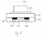
- Fig. 6 shows a cross sectional view of an apparatus for damping and monitoring emissions from a VCSEL according to a third embodiment of the present invention.
- This embodiment differs from the first and second embodiment in that: the substrate 116 is arranged between the VCSEL 114 and the damping layer 112, and the pair of electrodes, 110 and 111, is arranged below/on the lower surface of the substrate 116.
- the laser emission of the VCSEL 114 enters the substrate 116 at the upper surface thereof, traverses the substrate 116, leaves the substrate 116 at the lower surface thereof, thereafter enters the damping layer 112 at its (upper) surface contacting the lower surface of the substrate 116, traverses the damping layer 112, and leaves the damping layer 112 at its lower surface opposing the upper surface of the damping layer 112.
- the laser emission of the VCSEL 114 enters the damping layer 112 (at the upper surface thereof), traverses the damping layer 112, leaves the damping layer 112 (at the lower surface thereof), thereafter enters the substrate 116 at its (upper) surface contacting the lower surface of the damping layer 112, traverses the substrate 116, and leaves the substrate 116 at its lower surface opposing the upper surface of the substrate 116.
- the apparatus for damping and monitoring emissions from a VCSEL may comprise two or more cells/channels, each having a configuration as shown in Fig. 6 .
- the third embodiment may further comprise: another (second) VCSEL arranged above the upper surface of the substrate 116; another (second) damping layer which is isolated from the (first) damping layer and arranged below the substrate 116, so that at least a part of the other damping layer is deposited on the lower surface of the substrate 116; and another (second) pair of electrodes arranged on/below the lower surface of the substrate 116.
- the other damping layer is photosensitive to the laser emission of the other VCSEL and is adapted to decrease the power level of the laser emission of the other VCSEL to the desired level.
- Each electrode of the other pair of electrodes is in electrical contact with the other damping layer so as to collect free electric charges induced in the other damping layer by the laser emission of the other VCSEL.
- the other pair of electrodes is adapted to output another (second) signal corresponding to the power level of the laser emission of the other VCSEL.
- Figs. 7a, 7b and 7c show an apparatus for damping and monitoring emissions from a VCSEL according to a fourth embodiment of the present invention.
- This embodiment differs from the first, second and third embodiment in that: the substrate 216 is photosensitive to the laser emission of the VCSEL(s); the substrate 216 is adapted to decrease the power level of the laser emission of the VCSEL(s) by absorption, to the (predetermined) desired level; and the pair of electrodes, 110 and 111, needs to directly contact the upper surface and/or lower surface of the substrate 216 in order to collect the free electric charges induced by the laser emission of the VCSEL.
- the fourth embodiment of the present invention comprises: a VCSEL 114 for generating a laser emission; a (carrier) substrate 216 that is at least partially transparent to the laser emission of the VCSEL 114 and is adapted to carry the VCSEL 114 and eventually other electronic components; a pair of electrodes, 110 and 111, each of which being in direct contact with a surface of the substrate 216.
- the substrate 216 has a first surface and a second surface. Preferably, these surfaces are parallel and opposite to each other.
- the VCSEL 114 is arranged above the first (upper) surface of the substrate 216, so that the laser emission of the VCSEL 114 enters the substrate 216 at its first surface, traverses a region of the substrate 216 extending between the first surface and the second (lower) surface of the substrate 216, in the direction indicated by array 217, and leaves the substrate 216 at its second surface.
- the substrate 216 is photosensitive to the laser emission of the VCSEL 114. Therefore, the laser emission of the VCSEL 114 generates free electric charges in the region around/along the propagation direction 217, when passing/propagating through the substrate 216.
- the substrate 216 is (substantially) an electrical insulator in those regions where no laser emission is present. The amount of free charges created in the region around/along the propagation direction 217 corresponds to the power level of the laser emission of the VCSEL 114.
- Photoconductive polymers for instance, a polymer based on N-Vinylcarbazole, can be used as material for the substrate 216.
- the substrate 216 is adapted to decrease the power level of the laser emission of the VCSEL 114 by absorption, to the predetermined (desired level). This absorption occurs in the substrate 216, in the region along the propagation direction 217, while the laser emission propagates from the first (upper) surface of the substrate 216 to the second (lower) surface of the substrate 216.
- the term 'absorption' used here relates to both the deposition of radiation energy into (the medium of) the substrate and scattering processes in (the medium of) the substrate, deflecting the radiation from their initial propagation direction. Both energy deposition into (the medium of) the substrate and scattering processes attenuate the intensity of the laser emission (measured in W/m 2 ) propagating through the substrate 216.
- the transmission factor/transmittance of the substrate 216 which is the ratio between the intensity (in W/m 2 ) of the laser emission entering the substrate 216 at its first (upper) surface and the intensity (in W/m 2 ) of the laser emission leaving the substrate 216 at its second (lower) surface, is selected such that the intensity/power level of the laser emission leaving the substrate 216 is lower than the desired level (taking into consideration that the substrate 216 has a sufficient mechanical strength for carrying the VCSEL(s) and eventually the other electronic components).
- the desired level is an intensity/power level of the laser emission of the VCSEL 114 that is consistent with eye safety limits.
- each electrode of the pair of electrodes, 110 and 111 is (directly) deposited on the upper surface and/or lower surface of the substrate 216, so as to be able to collect free electric charges induced by the laser emission of the VCSEL in the region around/along the propagation direction 217 of the substrate 216. Furthermore, the pair of electrodes, 110 and 111, is adapted to output an electric signal corresponding to the intensity/power level of the laser emission of the VCSEL 114, based on the collected free electric charges.
- Fig. 7a shows a first example of the fourth embodiment, wherein the pair of electrodes, 110 and 111, is arranged between the VCSEL 114 and the substrate 216. Each electrode of the pair of electrodes, 110 and 111, is (directly) deposited on the first (upper) surface of the substrate 216.
- Fig. 7b shows a second example of the fourth embodiment, wherein the electrodes of the pair of electrodes, 110 and 111, are arranged on different/opposing surfaces of the substrate 216. For instance, the electrode 110 is (directly) deposited on the upper surface of the substrate 216, and the electrode 111 is (directly) deposited on the lower surface of the substrate 216.
- Fig. 7a shows a first example of the fourth embodiment, wherein the pair of electrodes, 110 and 111, is arranged between the VCSEL 114 and the substrate 216. Each electrode of the pair of electrodes, 110 and 111, is (directly) deposited on the first (upper) surface of the substrate 216.
- each electrode of the pair of electrodes, 110 and 111 is (directly) deposited on the lower surface of the substrate 216.
- each electrode of the pair of electrodes, 110 and 111 is in contact with the substrate 216 and positioned relative to the propagation direction 217 of the laser emission of the VCSEL 114, so that the pair of electrodes, 110 and 111, is able to collect free charges induced by the laser emission propagating along the direction 217.
- the apparatus for damping and monitoring emissions from a VCSEL may comprise two or more cells/channels, each having a configuration as shown in any of Figs. 7a, 7b and 7c .
- the fourth embodiment may further comprise: another (second) VCSEL arranged above the upper surface of the substrate 216; and another (second) pair of electrodes arranged on the upper surface and/or lower surface of the substrate 216.
- the substrate 216 also is photosensitive to the laser emission of the other VCSEL and adapted to decrease the power level of the laser emission of the other VCSEL by absorption, to the desired level.
- the other pair of electrodes is in (electrical) contact with the substrate 216 so as to collect free electric charges induced by the laser emission of the other VCSEL, and adapted to output another electrical signal corresponding to the power level of the laser emission of the other VCSEL.
- the first and second channels are separated by regions of the substrate where no laser emission will propagate. Consequently, these regions will have a permanent electrical resistance corresponding to an electrical insulator, irrespective of whether laser emission propagates along a channel or not. As the regions surrounding a channel are electrical insulators, the electric signal output by the pair of electrodes corresponding to one channel is not influenced by the laser emission of the VCSEL corresponding to another channel.
- the reference numerals 118 and 120 represent a polymer layer and an under-fill layer, respectively.
- An opto-electrical assembly (optical engine) comprises an apparatus according to the first or second embodiment, terminals 122 for connecting the VCSEL (or the array of VCSELs), and terminals for connecting electronic components, preferably a driver 102 for driving the VCSEL (or the array of VCSELs).
- the opto-electrical assembly according to the present invention can further comprise a polymer layer 118 deposited in an area of the upper surface of the glass substrate 116 which does not include a damping layer of the array of damping layers 112 or a contact area (terminal) of the array of contact areas 122.
- the opto-electrical assembly according to the present invention can comprise an underfill 120 between a VCSEL of the array of VCSELs 114 and its corresponding damping layer 112.
- the present invention is not limited only to VCSELs, but is also applicable to any laser devices emitting a laser emission; for instance, any type of laser diodes or optical fibers outputting a laser emission.
- the present invention is also applicable to light emitting diodes (LEDs).
- the apparatus for damping and monitoring emissions from a laser device performs both functions, the damping of the laser emission to a power level which is consistent with eye safety limits and the monitoring of the power level of the laser emission, by means of one and the same layer. Accordingly, the apparatus for damping and monitoring emissions from a laser device, according to the present invention, can be easily and cost-efficiently manufactured.
- Reference Numerals Reference Numeral Description 100 Opto-electrical assembly (optical engine) 101 Optical carrier (layer structure) 102 Driver IC 103 Array of VCSELs 104 Array of photodiodes 105 IC including transimpedance amplifiers (TIA) 106 Input terminals of driver IC 110, 111 Electrodes 112 Damping and monitoring layer 114 Vertical cavity surface emitting laser (VCSEL) 116 Glass substrate 118 Polymer layer 120 Under-fill layer 122 Contact areas for VCSELs 131 VCSEL array layer 132 Array of VCSELs 133 Contact areas on the VCSEL array layer 134 Layer of flex circuit 135 Contact areas on the layer of flex circuit 136 Amorphous silicon layer 137 Glass substrate 139 Array of pn detectors 140 Contact areas on the amorphous silicon layer 216 Substrate adapted for damping and monitoring 217 Propagation direction of the laser emission of a VCSEL
Abstract
Description
- The present invention relates to an apparatus for damping and monitoring emissions from a laser diode, particularly, from a vertical cavity surface emitting laser (VCSEL). Also, the present invention relates to an opto-electrical assembly (optical engine) including the apparatus for damping and monitoring emissions from a laser diode.
- In order to support the communication requirements of high-speed data transmission applications, optical links are used when links via an electrical wire have a too low bandwidth. When using an optical link for transmitting a signal from a first electronic component to a second electronic component, the electric signal to be transmitted is first converted into an optical signal, then the optical signal is coupled into an optical fiber via an optical transmitter and transmitted to the second electronic component via the optical fiber. On the other hand, when the first electronic component uses an optical link for receiving an optical signal from the second electronic component, the first electronic component converts the received optical signal into an electrical signal before further processing.
-
Fig. 1 shows an opto-electrical assembly (also denoted as optical engine) for converting an electric signal into an optical signal and vice-versa. Theoptical engine 100 includes anoptical carrier 101, an array of four laser diodes 103 (for instance, vertical cavity surface emitting lasers, abbreviated VCSEL), adriver IC 102 including an array of four drivers for driving the fourlaser diodes 103, an array of fourphotodiodes 104, and an integrated circuit (IC) including an array of four transimpedance amplifiers 105 (abbreviated TIAs) for amplifying the output signals of the fourphotodiodes 104. The driver IC 102, the array oflaser diodes 103, the array ofphotodiodes 104 and the IC including the TIAs 105 are all mounted on theoptical carrier 101. Theoptical carrier 101 essentially includes a glass substrate which is transparent for the light/laser emission of the optical signals. - Each driver of the
driver array 102 receives at itsinput terminals 106 an electric signal, converts the received electrical signal into an electric driver signal for driving a respective laser diode of the array oflaser diodes 103. Each laser diode of the array oflaser diodes 103 converts the driving signal received at its inputs to an optical signal, which is output to, for instance, an optical fiber (not shown inFig. 1 ). Each photodiode of the array ofphotodiodes 104 receives an optical signal from, for instance an optical fiber, converts the received optical signal into an electrical signal, and outputs this to the inputs of a respective TIA of the array ofTIAs 105. - When using laser diodes for converting electrical signals into optical signals, the
optical engine 100 has to meet standard eye safety regulations to avoid eye damage to an operator/user. Therefore, the output power of each optical signal which leaves theoptical engine 100 must not exceed eye safety limits. The power level of laser emissions output by vertical cavity surface emitting lasers (VCSELs) normally exceeds the eye safety limits. Therefore, damping/limiting/attenuating of the laser emissions output by VCSELs is required. In order to damp the optical power of the laser emission leaving theoptical engine 100, for instance, towards an optical fiber, a damping layer is used in known optical engines. This damping layer is interposed in the optical path of the laser emissions of the VCSELs. Typically, the damping layer is deposited on a surface of the glass substrate and integrated in theoptical carrier 101. The damping layer also reduces optical reflections toward VCSEL. - Furthermore, in fiber optic communication systems a nearly constant output power of the VCSELs is desired. However, during operation, ambient temperature changes and aging of the device can result in fluctuations in the output power of the VCSELs. Therefore, monitoring of the output power of the VCSELs is advantageous.
- To this end, document
US 6037644 discloses an apparatus for monitoring emissions from VCSELs.Fig. 2 shows a cross sectional view of this apparatus. It comprises: aglass substrate 137, anamorphous silicon layer 136 on theglass substrate 137, aseparate substrate 131 having selected areas being provided with theVCSELs 132, and aflex circuit layer 134 interposed between theamorphous silicon layer 136 and theseparate substrate 131. Theamorphous silicon layer 136 has selectively doped areas that providePN junctions 139 of photovoltaic devices and a sufficiently small optical absorption coefficient, within an optical wavelength range, that limits absorption of a corresponding small fractional amount of light being emitted by theVCSELs 132. Theamorphous silicon layer 136 and theglass substrate 137 are sufficiently thin to be transmissive of such light therethrough, excluding the small fractional amount of such light being absorbed by the photovoltaic devices. The photovoltaic devices are on top of the VCSELs. TheVCSELs 132 are further constructed and arranged to emit such light having a wavelength range that corresponds to the wavelength range at which theamorphous silicon layer 136 has the sufficiently small absorption coefficient, whereby, a substantial portion of such light is transmitted through the photovoltaic devices, and a small fraction of such light is absorbed by the dopedareas 139 of theamorphous silicon layer 136 to produce photovoltaic currents from the photovoltaic devices as a measurement of output power of theVCSELs 132. Theflex circuit layer 134 is transparent and includes on its upper and lower surface areas ofsemitransparent contact metallization 135. Theamorphous silicon layer 136 has semitransparentcontact metallization areas 140 being in contact with areas ofsemitransparent contact metallization 135 of the upper surface of the transparentflex circuit layer 134; and theseparate substrate 131 has respective semitransparentcontact metallization areas 132 being in contact with the areas ofsemitransparent contact metallization 135 of the lower surface of theflex circuit layer 140. - The apparatus for monitoring laser emissions from VCSELs shown in
Fig. 2 requires PN junctions 139 (i.e. photodiodes) for monitoring the output power of theVCSELs 132. However, implementing these PN junctions complicates the manufacturing process of the apparatus and consequently enhances its manufacturing costs. Also, the structure shown inFig. 2 requires theflex circuit layer 134 for providing electrical contacts to theVCSELs 132 and thephotodiodes 139, which further enhances the manufacturing costs. - It is, therefore, an objective of the present invention to provide for an apparatus for damping and monitoring emissions from a laser diode, particularly a VCSEL, which assures that the power of the laser emission that leaves/exits the apparatus meets eye safety limits, and provides a structure for monitoring the output power of the laser emission, which can be easily and cost-effectively manufactured.
- This objective is achieved by the features as set forth in claim 1. Further, advantageous embodiments of the present invention are set forth in the dependent claims.
- It is a further objective of the present invention to provide for an opto-electrical assembly (optical engine), which assures that the power of the laser emission that leaves/exits the opto-electrical assembly meets eye safety limits, enables monitoring the output power of this laser emission, and can be easily and cost-effectively manufactured.
- This objective is achieved by the features as set forth in independent claim 10.
- The present invention is based on the idea to deposit a photosensitive damping layer on the glass substrate of the apparatus, to contact the photosensitive damping layer with a pair of electrodes, and to adapt this pair of electrodes so as to output an electric signal in accordance with the power level of the laser emission of the laser diode.
- The apparatus according to the present invention needs no photodiode for monitoring the output power of the laser emission. Therefore, its manufacturing process is simplified and cost-effective.
-
- Fig. 1
- shows a perspective view of an opto-electrical assembly (optical engine);
- Fig. 2
- shows a cross sectional view of an apparatus for monitoring emissions from vertical cavity surface emitting lasers according to the prior art;
- Fig. 3
- shows a cross sectional view of an apparatus for damping and monitoring emissions from vertical cavity surface emitting lasers (VCSEL) according to a first embodiment of the present invention, at section A - A in
Fig. 1 ; - Fig. 4
- shows a plan view on the surface of the glass substrate of the apparatus according to the present invention, including contact areas for the VCSELs, the layers for damping and monitoring the laser emissions, and the electrodes for collecting the electric charges generated by the laser emission in respective layers for damping and monitoring the laser emissions;
- Fig. 5
- shows a cross sectional view of an apparatus for damping and monitoring emissions from a VCSEL according to a second embodiment of the present invention;
- Fig. 6
- shows a cross sectional view of an apparatus for damping and monitoring emissions from a VCSEL according to a third embodiment of the present invention;
- Figs. 7a, 7b and 7c
- show (a cross sectional view of) examples of an apparatus for damping and monitoring emissions from a VCSEL according to a fourth embodiment of the present invention.
-
Fig. 3 shows a cross-sectional view of an opto-electrical assembly according to the present invention, at section A - A indicated inFig. 1 . The opto-electrical assembly (optical engine), according to the present invention, includes an apparatus for damping and monitoring emissions from VCSELs according to the present invention.Fig. 3 also represents a cross-sectional view of an apparatus for damping and monitoring emissions from VCSELs, according to a first embodiment of the present invention. - The apparatus, according to the first embodiment of the present invention, comprises: a
glass substrate 116, an array of fourdamping layers 112, an array of four pairs of electrodes, an array of four VCSELs, apolymer layer 118, andunderfill 120. Theglass substrate 116, the array ofdamping layers 112, the array of pairs of electrodes, and thepolymer layer 118 form anoptical carrier 101, on which the array of VCSELs is mounted. Typically, the array of VCSELs is arranged in anextra component 103, which is fixed on theoptical carrier 101 by means ofunderfill 120. - Each VCSEL of the array of
VCSELs 114 is adapted to receive an electric driver signal from an associated driver and to convert the received electric driver signal into an optical signal, by outputting a laser emission corresponding to the electric driver signal. In the apparatus ofFig. 3 , the propagation direction of the laser emission of each VCSEL of the array ofVCSELs 114 is downwards, perpendicular to theglass substrate 116. The propagation direction of the laser emission does not have to be perpendicular to theglass substrate 116, but can also be inclined/oblique relative to the (light incident surface of the)glass substrate 116. - Each damping layer of the array of damping
layers 112 is provided on theglass substrate 116. The array ofVCSELs 114, the array of dampinglayers 112 and the glass substrate are arranged in such a way that the laser emission of each VCSEL of the array ofVCSELs 114 propagates/traverses the respective damping layer of the array of dampinglayers 112 and theglass substrate 116. In the apparatus shown inFig. 3 , the upper and lower surface of each dampinglayer 112 is (substantially) perpendicular to the propagation direction of the laser emission of the respective VCSEL. The area of the dampinglayer 112 is greater than the cross-sectional area of the laser beam of therespective VCSEL 114. Also, each dampinglayer 112 is arranged between therespective VCSEL 114 and theglass substrate 116, so that the laser emission emerging from the respective VCSEL traverses first the dampinglayer 112 and then theglass substrate 116. Furthermore, each damping layer of the array of dampinglayers 112 is adapted to decrease/attenuate/damp the power level of the laser emission of itsrespective VCSEL 114 by absorption. Specifically, each dampinglayer 112 attenuates the power level of a laser emission that is incident on the upper surface of the dampinglayer 112, by a predetermined amount, so that the power level of the laser emission exiting the lower surface of each dampinglayer 112 meets eye safety limits. The predetermined amount is, for example, 10% or more. As a result, the power level of the laser emission emerging the lower surface of theglass substrate 116 is sufficiently lowered compared to the power level of the laser emission emerging the output of the VCSEL, so that the laser emission emerging the lower surface of theglass substrate 116 does not pose a danger for a human being, particularly an eye damage. In other words, the power level of the laser emission emerging (the lower surface of) theglass substrate 116 does not exceed a predetermined power level, wherein the predetermined power level is consistent with eye safety limits. - The
glass substrate 116 usually shows a very low absorption coefficient for the laser emission. Therefore, theglass substrate 116 is considered to be (substantially) transparent to the laser emission of theVCSELs 114. Also, the present invention is not limited to a glass substrate, but may include, instead of theglass substrate 116, any substrate showing a low, preferably insignificant, absorption/attenuation coefficient for the laser emission. - According to the present invention, the damping layers of the array of damping
layers 112 are isolated, particularly electrically isolated, from each other; and each damping layer of the array of dampinglayers 112 is photosensitive to the laser emission of itsrespective VCSEL 114. This means that a laser emission passing through a dampinglayer 112 generates electron-hole pairs, i.e. free charge carriers, in the respective damping layer, thereby altering its electrical conductive. The number of electron-hole pairs generated in the dampinglayer 112, and thus its electrical conductivity, corresponds to the power level of the laser emission that is incident to the upper surface of the damping layer. The electrical conductivity of the dampinglayer 112 increases when the power level of the incident laser emission increases. For example, the dampinglayer 112 is (or acts as) a photoresistor. - In the apparatus for damping and monitoring emissions from VCSELs, according to the present invention, any/each damping layer of the array of damping
layers 112 includes, for example, silicon - preferentially amorphous silicon, because amorphous silicon can be easily deposited on the glass substrate, e.g. by RF-sputtering, and has lower scattering losses than poly-crystal silicon. Mono-crystal silicon can also be used for the dampinglayer 112, especially if the optical carrier is build of silicon wafer. - Also, according to the present invention, the electrodes (110, 111) of each pair of electrodes of the array of pairs of electrodes are in direct contact with a respective damping
layer 112, so that the electrodes (110, 111) can collect the free charge carriers induced by the laser emission that passes through the respective dampinglayer 112. Furthermore, each pair of electrodes is adapted to sense the change of the electrical conductivity of the respective dampinglayer 112, when a laser emission passes through the respective damping layer, and to output an electric signal corresponding to the power level of the laser emission that is incident onto the respective dampinglayer 112. This electric signal is suitable for monitoring the power level of the laser emission, for instance, by thedriver IC 102 or any other device. Any/Each pair of electrodes of the array of pairs of electrodes are connectable to respective inputs of thedriver IC 102 or any other device. -
Transparent electrodes 110 and 111 (for instance, formed of indium tin oxide, ITO) are advantageous for the present invention, if theelectrodes layer 112 are arranged close to each other, so that the laser emission passing through the respective damping layer crosses one or bothelectrodes - In the apparatus according to the first embodiment, shown in
Fig. 3 , the electrodes (110, 111) of each pair of electrodes and a part (preferably the middle part) of each dampinglayer 112 are deposited, preferably directly, on the upper surface of theglass substrate 116; and another part (preferably a peripheral part) of each dampinglayer 112 is deposited, preferably directly, on theelectrodes layer 112. The (layer) structure of the apparatus according to the first embodiment also becomes evident fromFig. 4 . -
Fig. 4 shows a plan view of the optical carrier which does not have thepolymer layer 118. An apparatus for damping and monitoring emissions from VCSELs including the optical carrier shown inFig. 4 is also in accordance with the first embodiment of the present invention. -
Fig. 4 shows the damping layers of the array of dampinglayers 112, their associated pair of electrodes (100, 111) of the array of pairs of electrodes, and an array ofcontact areas 122 for contacting/connecting inputs of the VCSELs of the array of VCSELs to respective outputs of the driver IC 102 (the VCSELs and the driver IC are not shown inFig. 4 ). This figure clearly shows that the damping layers of the array of dampinglayers 112 are isolated from each other. It is further evident fromFigs. 3 and 4 that each electrode of each pair of electrodes includes a layer arranged between a peripheral/marginal portion of its associated dampinglayer 112 and theglass substrate 116, and that this peripheral portion of the dampinglayer 112 is deposited, preferably directly, on the layer of the respective electrode. This (layer) structure is in accordance with the present invention, and has the advantage that it can be easily and cost-effectively manufactured. - However, it is not mandatory for the first embodiment of the present invention that a part of the damping layer is deposited on the electrodes contacting the respective damping layer. It is sufficient that the electrodes contact lateral faces of the respective damping layer.
- Also, it is not mandatory for the first embodiment of the present invention that the damping layers and the pairs of electrodes are provided between the VCSELs and the glass substrate. The effect of damping and monitoring the laser emission of the VCSEL can be achieved also if the damping layers and their associated pairs of electrodes can be provided/deposited on the lower surface of the glass substrate, i.e. the surface being more distant from the respective VCSEL.
-
Figs. 3 and 4 show an embodiment of the present invention including four cells/channels for converting an electrical driving signal into an optical signal. However, the present invention is also applicable to an apparatus for damping and monitoring emissions from a laser device, including any plurality of cells/channels. Also, the present invention is applicable to an embodiment including a single cell/channel. -
Fig. 5 shows a cross-sectional view of a single cell of the array shown inFig 3 . This cell represents a second embodiment of the present invention. For convenience, components (or layers) inFig. 5 that are similar or identical to corresponding components (or layers) inFigs. 3 and 4 are assigned the same reference numbers. - The apparatus, according to the second embodiment of the present invention, comprises: a
glass substrate 116, a dampinglayer 112, a pair of electrodes, a VCSEL, apolymer layer 118, andunderfill 120. Theglass substrate 116, the dampinglayer 112, the pair of electrodes, and thepolymer layer 118 form an optical carrier, on which the VCSEL is mounted. Typically, the VCSEL is arranged in an extra component, which is fixed on the optical carrier by means ofunderfill 120. - The
VCSEL 114 is adapted to receive an electric driver signal from an associated driver and to convert the received electric driver signal into an optical signal, by outputting a laser emission corresponding to the electric driver signal. In the apparatus ofFig. 5 , the propagation direction of the laser emission of theVCSEL 114 is downwards, perpendicular to theglass substrate 116. However, in the present invention, the propagation direction of the laser emission does not have to be perpendicular to theglass substrate 116. The propagation direction of the laser emission can also be inclined relative to the (light incident surface of the)glass substrate 116. - The damping
layer 112 corresponding to theVCSEL 114 is arranged in the propagation direction of the laser emission of the VCSEL. Preferably, the cross-sectional area of the dampinglayer 112 is (substantially) perpendicular to the propagation direction of the laser emission of the VCSEL, and/or the cross-sectional area of the dampinglayer 112 is equal to, or greater than, the cross-sectional area of the laser emission of theVCSEL 114. In the embodiment shown inFig. 5 , the dampinglayer 112 is arranged between theVCSEL 114 and theglass substrate 116, so that the laser emission emerging from the VCSEL is incident on the upper surface of the dampinglayer 112. - The damping
layer 112 is adapted to decrease/attenuate/damp the power level of the laser emission of theVCSEL 114 by absorption. For instance, the dampinglayer 112 is adapted to attenuate the power level of the laser emission that is incident on the upper surface of the dampinglayer 112, by a predetermined amount, so that the power level of the laser emission exiting the lower surface of the dampinglayer 112 meets eye safety limits. The predetermined amount is, for example, 10% or more. As theglass substrate 116 usually has a non-zero absorption coefficient for the laser emission (though this is very low) and the laser emission emerging the VCSEL is subjected to attenuation/absorption by the dampinglayer 112 and to absorption by theglass substrate 116, it is sufficient for the present invention (including both the first and second embodiment) that the dampinglayer 112 is adapted such that the combined absorption by both the dampinglayer 112 and theglass substrate 116 attenuates the power level of the laser emission emerging the VCSEL to a predetermined power level which is consistent with eye safety limits. Accordingly, the power level of the laser emission emerging theglass substrate 116 is limited to the predetermined power level. - According to the present invention, the power level of the laser emission emerging the lower surface of the
glass substrate 116 is sufficiently lowered compared to the power level of the laser emission emerging the output of the VCSEL, so that the laser emission emerging the lower surface of theglass substrate 116 does not pose a danger for a human being, particularly for eye damage. - However, the present invention is not limited to apparatuses/applications for damping and monitoring emissions from a laser device, wherein the power level of the laser emission leaving the glass substrate/damping layer is limited to a (predetermined) level that is consistent with eye safety limits, but subsumes/covers also apparatuses/applications, wherein the power level of the laser emission leaving the glass substrate/damping layer is limited to any (predetermined) desired level.
- According to the present invention, the damping
layer 112 is photosensitive to the laser emission of theVCSEL 114. The electrical conductivity of the dampinglayer 112 corresponds to the power level of the laser emission that is incident to the upper surface of the damping layer. For example, the dampinglayer 112 is a photoresistor. The dampinglayer 112 includes silicon, preferably amorphous silicon. Mono-crystal silicon can also be used for the dampinglayer 112, especially if the optical carrier is build of silicon wafer. - Also, according to the present invention, the electrodes (110, 111) of the pair of electrodes are in direct contact with the damping
layer 112, so that the electrodes (110, 111) can collect the free charge carriers induced by the laser emission that passes through the dampinglayer 112. Furthermore, the pair of electrodes is adapted to sense the change of the electrical conductivity of the dampinglayer 112, when a laser emission passes through the damping layer, and to output an electric signal corresponding to the power level of the laser emission that is incident onto the dampinglayer 112. This signal can be used for monitoring the power level of the laser emission. - If the
electrodes layer 112 crosses/intersects one or both electrodes (110, 111), it is advantageous for the present invention that theelectrodes - In the apparatus, according to the second embodiment, the
electrodes layer 112 are deposited, preferably directly, on the upper surface of theglass substrate 116. Theelectrode 110 includes a layer arranged between a first portion of the dampinglayer 112 and theglass substrate 116, and the first portion of the dampinglayer 112 is deposited (preferably directly) on the layer of theelectrode 110. Theelectrode 111 includes a layer arranged between a second portion of the dampinglayer 112 and theglass substrate 116, and the second portion of the dampinglayer 112 is deposited (preferably directly) on the layer of theelectrode 111. Preferably, the first portion and/or the second portion of the first dampinglayer 112 are peripheral regions of the dampinglayer 112. - It is not mandatory for the second embodiment of the present invention that a part of the damping layer is deposited on the electrodes contacting the damping layer. It is sufficient that the electrodes contact lateral faces of the damping layer.
- Also, it is not mandatory for the second embodiment of the present invention that the damping layer and the pair of electrodes are provided between the VCSEL and the glass substrate. The effect of damping and monitoring the laser emission of the VCSEL can be achieved also if the damping layer and the pair of electrodes can be provided/deposited on the lower surface of the glass substrate, i.e. the surface being more distant from the VCSEL.
-
Fig. 6 shows a cross sectional view of an apparatus for damping and monitoring emissions from a VCSEL according to a third embodiment of the present invention. This embodiment differs from the first and second embodiment in that: thesubstrate 116 is arranged between theVCSEL 114 and the dampinglayer 112, and the pair of electrodes, 110 and 111, is arranged below/on the lower surface of thesubstrate 116. - In the third embodiment of the present invention, the laser emission of the
VCSEL 114 enters thesubstrate 116 at the upper surface thereof, traverses thesubstrate 116, leaves thesubstrate 116 at the lower surface thereof, thereafter enters the dampinglayer 112 at its (upper) surface contacting the lower surface of thesubstrate 116, traverses the dampinglayer 112, and leaves the dampinglayer 112 at its lower surface opposing the upper surface of the dampinglayer 112. However, in the first and second embodiment, the laser emission of theVCSEL 114 enters the damping layer 112 (at the upper surface thereof), traverses the dampinglayer 112, leaves the damping layer 112 (at the lower surface thereof), thereafter enters thesubstrate 116 at its (upper) surface contacting the lower surface of the dampinglayer 112, traverses thesubstrate 116, and leaves thesubstrate 116 at its lower surface opposing the upper surface of thesubstrate 116. - The apparatus for damping and monitoring emissions from a VCSEL according to the third embodiment may comprise two or more cells/channels, each having a configuration as shown in
Fig. 6 . Specifically, the third embodiment may further comprise: another (second) VCSEL arranged above the upper surface of thesubstrate 116; another (second) damping layer which is isolated from the (first) damping layer and arranged below thesubstrate 116, so that at least a part of the other damping layer is deposited on the lower surface of thesubstrate 116; and another (second) pair of electrodes arranged on/below the lower surface of thesubstrate 116. The other damping layer is photosensitive to the laser emission of the other VCSEL and is adapted to decrease the power level of the laser emission of the other VCSEL to the desired level. Each electrode of the other pair of electrodes is in electrical contact with the other damping layer so as to collect free electric charges induced in the other damping layer by the laser emission of the other VCSEL. The other pair of electrodes is adapted to output another (second) signal corresponding to the power level of the laser emission of the other VCSEL. -
Figs. 7a, 7b and 7c show an apparatus for damping and monitoring emissions from a VCSEL according to a fourth embodiment of the present invention. This embodiment differs from the first, second and third embodiment in that: thesubstrate 216 is photosensitive to the laser emission of the VCSEL(s); thesubstrate 216 is adapted to decrease the power level of the laser emission of the VCSEL(s) by absorption, to the (predetermined) desired level; and the pair of electrodes, 110 and 111, needs to directly contact the upper surface and/or lower surface of thesubstrate 216 in order to collect the free electric charges induced by the laser emission of the VCSEL. - The fourth embodiment of the present invention comprises: a
VCSEL 114 for generating a laser emission; a (carrier)substrate 216 that is at least partially transparent to the laser emission of theVCSEL 114 and is adapted to carry theVCSEL 114 and eventually other electronic components; a pair of electrodes, 110 and 111, each of which being in direct contact with a surface of thesubstrate 216. Thesubstrate 216 has a first surface and a second surface. Preferably, these surfaces are parallel and opposite to each other. TheVCSEL 114 is arranged above the first (upper) surface of thesubstrate 216, so that the laser emission of theVCSEL 114 enters thesubstrate 216 at its first surface, traverses a region of thesubstrate 216 extending between the first surface and the second (lower) surface of thesubstrate 216, in the direction indicated byarray 217, and leaves thesubstrate 216 at its second surface. - According to the fourth embodiment, the
substrate 216 is photosensitive to the laser emission of theVCSEL 114. Therefore, the laser emission of theVCSEL 114 generates free electric charges in the region around/along thepropagation direction 217, when passing/propagating through thesubstrate 216. However, thesubstrate 216 is (substantially) an electrical insulator in those regions where no laser emission is present. The amount of free charges created in the region around/along thepropagation direction 217 corresponds to the power level of the laser emission of theVCSEL 114. Photoconductive polymers, for instance, a polymer based on N-Vinylcarbazole, can be used as material for thesubstrate 216. - Furthermore, the
substrate 216 is adapted to decrease the power level of the laser emission of theVCSEL 114 by absorption, to the predetermined (desired level). This absorption occurs in thesubstrate 216, in the region along thepropagation direction 217, while the laser emission propagates from the first (upper) surface of thesubstrate 216 to the second (lower) surface of thesubstrate 216. The term 'absorption' used here relates to both the deposition of radiation energy into (the medium of) the substrate and scattering processes in (the medium of) the substrate, deflecting the radiation from their initial propagation direction. Both energy deposition into (the medium of) the substrate and scattering processes attenuate the intensity of the laser emission (measured in W/m2) propagating through thesubstrate 216. - Therefore, in accordance with the fourth embodiment of the present invention, the transmission factor/transmittance of the
substrate 216, which is the ratio between the intensity (in W/m2) of the laser emission entering thesubstrate 216 at its first (upper) surface and the intensity (in W/m2) of the laser emission leaving thesubstrate 216 at its second (lower) surface, is selected such that the intensity/power level of the laser emission leaving thesubstrate 216 is lower than the desired level (taking into consideration that thesubstrate 216 has a sufficient mechanical strength for carrying the VCSEL(s) and eventually the other electronic components). For instance, the desired level is an intensity/power level of the laser emission of theVCSEL 114 that is consistent with eye safety limits. - According to the fourth embodiment, each electrode of the pair of electrodes, 110 and 111, is (directly) deposited on the upper surface and/or lower surface of the
substrate 216, so as to be able to collect free electric charges induced by the laser emission of the VCSEL in the region around/along thepropagation direction 217 of thesubstrate 216. Furthermore, the pair of electrodes, 110 and 111, is adapted to output an electric signal corresponding to the intensity/power level of the laser emission of theVCSEL 114, based on the collected free electric charges. -
Fig. 7a shows a first example of the fourth embodiment, wherein the pair of electrodes, 110 and 111, is arranged between theVCSEL 114 and thesubstrate 216. Each electrode of the pair of electrodes, 110 and 111, is (directly) deposited on the first (upper) surface of thesubstrate 216.Fig. 7b shows a second example of the fourth embodiment, wherein the electrodes of the pair of electrodes, 110 and 111, are arranged on different/opposing surfaces of thesubstrate 216. For instance, theelectrode 110 is (directly) deposited on the upper surface of thesubstrate 216, and theelectrode 111 is (directly) deposited on the lower surface of thesubstrate 216.Fig. 7c shows a third example of the fourth embodiment, wherein the pair of electrodes, 110 and 111, is arranged on the surface of thesubstrate 216 being more distant from theVCSEL 114. Specifically, each electrode of the pair of electrodes, 110 and 111, is (directly) deposited on the lower surface of thesubstrate 216. - In the first, second and third example of the fourth embodiment, each electrode of the pair of electrodes, 110 and 111, is in contact with the
substrate 216 and positioned relative to thepropagation direction 217 of the laser emission of theVCSEL 114, so that the pair of electrodes, 110 and 111, is able to collect free charges induced by the laser emission propagating along thedirection 217. - The apparatus for damping and monitoring emissions from a VCSEL according to the fourth embodiment may comprise two or more cells/channels, each having a configuration as shown in any of
Figs. 7a, 7b and 7c . Specifically, the fourth embodiment may further comprise: another (second) VCSEL arranged above the upper surface of thesubstrate 216; and another (second) pair of electrodes arranged on the upper surface and/or lower surface of thesubstrate 216. Thesubstrate 216 also is photosensitive to the laser emission of the other VCSEL and adapted to decrease the power level of the laser emission of the other VCSEL by absorption, to the desired level. The other pair of electrodes is in (electrical) contact with thesubstrate 216 so as to collect free electric charges induced by the laser emission of the other VCSEL, and adapted to output another electrical signal corresponding to the power level of the laser emission of the other VCSEL. The first and second channels are separated by regions of the substrate where no laser emission will propagate. Consequently, these regions will have a permanent electrical resistance corresponding to an electrical insulator, irrespective of whether laser emission propagates along a channel or not. As the regions surrounding a channel are electrical insulators, the electric signal output by the pair of electrodes corresponding to one channel is not influenced by the laser emission of the VCSEL corresponding to another channel. - In
Figs. 6 ,7a, 7b and 7c , thereference numerals - An opto-electrical assembly (optical engine) according to the present invention comprises an apparatus according to the first or second embodiment,
terminals 122 for connecting the VCSEL (or the array of VCSELs), and terminals for connecting electronic components, preferably adriver 102 for driving the VCSEL (or the array of VCSELs). The opto-electrical assembly according to the present invention can further comprise apolymer layer 118 deposited in an area of the upper surface of theglass substrate 116 which does not include a damping layer of the array of dampinglayers 112 or a contact area (terminal) of the array ofcontact areas 122. Furthermore, the opto-electrical assembly according to the present invention can comprise anunderfill 120 between a VCSEL of the array ofVCSELs 114 and its corresponding dampinglayer 112. - The present invention is not limited only to VCSELs, but is also applicable to any laser devices emitting a laser emission; for instance, any type of laser diodes or optical fibers outputting a laser emission. The present invention is also applicable to light emitting diodes (LEDs).
- The apparatus for damping and monitoring emissions from a laser device, according to the present invention, performs both functions, the damping of the laser emission to a power level which is consistent with eye safety limits and the monitoring of the power level of the laser emission, by means of one and the same layer. Accordingly, the apparatus for damping and monitoring emissions from a laser device, according to the present invention, can be easily and cost-efficiently manufactured.
Reference Numerals Reference Numeral Description 100 Opto-electrical assembly (optical engine) 101 Optical carrier (layer structure) 102 Driver IC 103 Array of VCSELs 104 Array of photodiodes 105 IC including transimpedance amplifiers (TIA) 106 Input terminals of driver IC 110, 111 Electrodes 112 Damping and monitoring layer 114 Vertical cavity surface emitting laser (VCSEL) 116 Glass substrate 118 Polymer layer 120 Under- fill layer 122 Contact areas for VCSELs 131 VCSEL array layer 132 Array of VCSELs 133 Contact areas on the VCSEL array layer 134 Layer of flex circuit 135 Contact areas on the layer of flex circuit 136 Amorphous silicon layer 137 Glass substrate 139 Array of pn detectors 140 Contact areas on the amorphous silicon layer 216 Substrate adapted for damping and monitoring 217 Propagation direction of the laser emission of a VCSEL
Claims (15)
- An apparatus for damping and monitoring emissions from a light emitting device, comprising:a substrate that is at least partially transparent (116), preferably glass;a first light emitting device (114), preferably a vertical cavity surface emitting laser (VCSEL), for generating light emission;a first damping layer (112), preferably of amorphous silicon, for decreasing the power level of the light emission of the first light emitting device (114) by absorption, to a desired level,wherein at least a part of the first damping layer (112) is deposited on a surface of the substrate (116), andthe first damping layer (112) is photosensitive to the light emission of the first light emitting device (114); anda first pair of electrodes (110, 111), each of which being in direct contact with the first damping layer (112), for outputting a first electric signal corresponding to the power level of the light emission of the first light emitting device (114).
- The apparatus according to claim 1, wherein the first damping layer (112) is arranged between the first light emitting device (114) and the substrate (116).
- The apparatus according to claim 1, wherein the substrate (116) is arranged between the first light emitting device (114) and the first damping layer (112).
- The apparatus according to any of claims 1 to 3, wherein a first electrode (110) of the first pair of electrodes is deposited on the surface of the substrate (116), and/or
a second electrode (111) of the first pair of electrodes is deposited on the surface of the substrate (116). - The apparatus according to claim 4, wherein the first electrode (110) of the first pair of electrodes includes a layer arranged between a first portion of the first damping layer (112) and the substrate (116), and the first portion of the first damping layer (112) is deposited on the layer of the first electrode (110) of the first pair of electrodes; and/or
the second electrode (111) of the first pair of electrodes includes a layer arranged between a second portion of the first damping layer (112) and the substrate (116), and the second portion of the first damping layer (112) is deposited on the layer of the second electrode (111) of the first pair of electrodes;
preferably, the first portion and/or the second portion of the first damping layer (112) are peripheral regions of the first damping layer. - The apparatus according to claim 4 or 5, wherein an electrode of the first pair of electrodes (110, 111) includes indium tin oxide.
- The apparatus according to any of claims 1 to 6, further comprising:a second light emitting device, preferably a vertical cavity surface emitting laser (VCSEL), for generating light emission;a second damping layer, preferably of amorphous silicon, for decreasing the power level of the light emission of the second light emitting device to a desired level,wherein at least a part of the second damping layer is deposited on the surface of the substrate,the second damping layer is photosensitive to the emission of the second light emitting device, andthe second damping layer is isolated from the first damping layer; anda second pair of electrodes, each of which being in direct contact with the second damping layer, for outputting a second electric signal corresponding to the power level of the light emission of the second light emitting device.
- An apparatus for damping and monitoring emissions from a light emitting device, comprising:a substrate (216) that is at least partially transparent;a light emitting device (114), preferably a vertical cavity surface emitting laser (VCSEL),for generating light emission; anda pair of electrodes (110, 111), each of which being in direct contact with a surface of the substrate (216),wherein the light emission enters the substrate (216) at a first surface thereof, traverses a region of the substrate (216) extending between the first surface and a second surface of the substrate, and leaves the substrate (216) at the second surface thereof,preferably, the first surface and the second surface of the substrate (216) are opposite to each other,the substrate (216) is photosensitive to the light emission of the light emitting device (114) and is adapted to decrease the power level of the light emission of the light emitting device (114) by absorption, to a desired level, andthe pair of electrodes (110, 111) is adapted to output an electric signal corresponding to the power level of the light emission of the light emitting device (114), based on the free electric charges induced by the light emission in the region of the substrate.
- The apparatus according to claim 8, wherein both electrodes of the pair of electrodes (110, 111) are arranged on either the first surface or the second surface; or
the first electrode of the pairs of electrodes (110, 111) is arranged on the first surface and the second electrode of the pairs of electrodes (110, 111) is arranged on the second surface. - An apparatus for damping and monitoring emissions from a light emitting device, comprising:a substrate (116) that is at least partially transparent, preferably formed of glass;a plurality of light emitting devices, preferably vertical cavity surface emitting lasers (VCSELs), each light emitting device (114) of the plurality of light emitting devices is adapted to generate light emission;a plurality of damping layers, preferably of amorphous silicon, each damping layer (112) of the plurality of damping layers being associated with a respective light emitting device (114) of the plurality of light emitting devices,wherein each damping layer (112) of the plurality of damping layers is arranged in propagation direction of the light emission of its associated light emitting device (114) of the plurality of light emitting devices,each damping layer (112) of the plurality of damping layers is adapted to decrease the power level of the light emission of its associated light emitting device (114) of the plurality of light emitting devices by absorption, to a desired level,at least a part of each damping layer (112) of the plurality of damping layers is deposited on a surface of the substrate (116),each damping layer (112) of the plurality of damping layers is photosensitive to the light emission of its associated light emitting device (114) of the plurality of light emitting devices, andthe damping layers of the plurality of damping layers are isolated from each other; anda plurality of pairs of electrodes, each pair of electrodes (110, 111) of the plurality of pairs of electrodes is associated with a respective damping layer (112) of the plurality of damping layers and is associated with the light emitting device (114) of the plurality of light emitting devices which is associated with the respective damping layer (112),wherein each electrode of each pair of electrodes (110, 111) of the plurality of pairs of electrodes is in direct contact with the damping layer (112) of the plurality of damping layers which is associated with the respective pair of electrodes (110, 111), andeach pair of electrodes (110, 111) of the plurality of pairs of electrodes is adapted to output an electric signal corresponding to the power level of the light emission of its associated light emitting device (114) of the plurality of light emitting devices.
- The apparatus according to claim 10, wherein each damping layer (112) of the plurality of damping layers is arranged between its associated light emitting device (114) of the plurality of light emitting devices and the substrate (116).
- The apparatus according to claim 10 or 11, wherein a first electrode (110) of each pair of electrodes of the plurality of pairs of electrodes is deposited on the surface of the substrate (116),
the first electrode (110) of each pair of electrodes of the plurality of pairs of electrodes includes a layer arranged between a first portion of its associated damping layer (112) of the plurality of damping layers and the substrate (116),
the first portion of its associated damping layer (112) of the plurality of damping layers is deposited on the layer of the first electrode (110) of the respective pair of electrodes of the plurality of pairs of electrodes,
a second electrode (111) of each pair of electrodes of the plurality of pairs of electrodes is deposited on the surface of the substrate (116),
the second electrode (111) of each pair of electrodes of the plurality of pairs of electrodes includes a layer arranged between a second portion of its associated damping layer (112) of the plurality of damping layers and the substrate (116), and
the second portion of its associated damping layer (112) of the plurality of damping layers is deposited on the layer of the second electrode (111) of the respective pair of electrodes of the plurality of pairs of electrodes,
preferably, the first portion and the second portion of each damping layer of the plurality of damping layers are peripheral regions of the respective damping layer. - An opto-electrical assembly comprising:an apparatus according to any of claims 1 to 12,terminals (122) for connecting a light emitting device of said apparatus, andterminals for connecting electronic components, preferably the electronic component is a driver (102) for driving a light emitting device of said apparatus.
- The opto-electrical assembly according to claim 13, further comprising a polymer layer (118) deposited in an area of the surface of the substrate (116) which does not include a damping layer (112) of said apparatus or a terminal (122).
- The opto-electrical assembly according to claim 14, further comprising an underfill (120) between a light emitting device (114) of said apparatus and its corresponding damping layer (112).
Priority Applications (2)
| Application Number | Priority Date | Filing Date | Title |
|---|---|---|---|
| EP15195655.4A EP3171464A1 (en) | 2015-11-20 | 2015-11-20 | Apparatus for damping and monitoring emissions from light emitting devices |
| US15/411,828 US10141715B2 (en) | 2015-11-20 | 2017-01-20 | Apparatus for damping and monitoring emissions from light emitting devices |
Applications Claiming Priority (1)
| Application Number | Priority Date | Filing Date | Title |
|---|---|---|---|
| EP15195655.4A EP3171464A1 (en) | 2015-11-20 | 2015-11-20 | Apparatus for damping and monitoring emissions from light emitting devices |
Publications (1)
| Publication Number | Publication Date |
|---|---|
| EP3171464A1 true EP3171464A1 (en) | 2017-05-24 |
Family
ID=54695582
Family Applications (1)
| Application Number | Title | Priority Date | Filing Date |
|---|---|---|---|
| EP15195655.4A Withdrawn EP3171464A1 (en) | 2015-11-20 | 2015-11-20 | Apparatus for damping and monitoring emissions from light emitting devices |
Country Status (2)
| Country | Link |
|---|---|
| US (1) | US10141715B2 (en) |
| EP (1) | EP3171464A1 (en) |
Families Citing this family (2)
| Publication number | Priority date | Publication date | Assignee | Title |
|---|---|---|---|---|
| JP6674428B2 (en) * | 2017-10-04 | 2020-04-01 | 日本電信電話株式会社 | Semiconductor light receiving parts |
| US10659166B2 (en) * | 2017-12-20 | 2020-05-19 | Finisar Corporation | Integrated optical transceiver |
Citations (4)
| Publication number | Priority date | Publication date | Assignee | Title |
|---|---|---|---|---|
| EP0899836A1 (en) * | 1997-08-27 | 1999-03-03 | Xerox Corporation | Semiconductor laser device |
| US6037644A (en) | 1997-09-12 | 2000-03-14 | The Whitaker Corporation | Semi-transparent monitor detector for surface emitting light emitting devices |
| US20030057355A1 (en) * | 2001-09-24 | 2003-03-27 | Cheng-Bin Wang | Auto feedback and photo attenuation structure of vertical cavity surface emitting laser |
| US6879014B2 (en) * | 2000-03-20 | 2005-04-12 | Aegis Semiconductor, Inc. | Semitransparent optical detector including a polycrystalline layer and method of making |
Family Cites Families (3)
| Publication number | Priority date | Publication date | Assignee | Title |
|---|---|---|---|---|
| US5141308A (en) * | 1991-08-12 | 1992-08-25 | Danckwerth Thomas M | Semiconductor laser pulse compression radar system |
| US5606572A (en) * | 1994-03-24 | 1997-02-25 | Vixel Corporation | Integration of laser with photodiode for feedback control |
| DK2775806T3 (en) * | 2013-03-07 | 2015-06-01 | Tyco Electronics Svenska Holdings Ab | Optical receiver and transceiver operating this |
-
2015
- 2015-11-20 EP EP15195655.4A patent/EP3171464A1/en not_active Withdrawn
-
2017
- 2017-01-20 US US15/411,828 patent/US10141715B2/en active Active
Patent Citations (4)
| Publication number | Priority date | Publication date | Assignee | Title |
|---|---|---|---|---|
| EP0899836A1 (en) * | 1997-08-27 | 1999-03-03 | Xerox Corporation | Semiconductor laser device |
| US6037644A (en) | 1997-09-12 | 2000-03-14 | The Whitaker Corporation | Semi-transparent monitor detector for surface emitting light emitting devices |
| US6879014B2 (en) * | 2000-03-20 | 2005-04-12 | Aegis Semiconductor, Inc. | Semitransparent optical detector including a polycrystalline layer and method of making |
| US20030057355A1 (en) * | 2001-09-24 | 2003-03-27 | Cheng-Bin Wang | Auto feedback and photo attenuation structure of vertical cavity surface emitting laser |
Also Published As
| Publication number | Publication date |
|---|---|
| US20170264077A1 (en) | 2017-09-14 |
| US10141715B2 (en) | 2018-11-27 |
Similar Documents
| Publication | Publication Date | Title |
|---|---|---|
| US8183656B2 (en) | Photodiode | |
| KR102345934B1 (en) | Method and system for germanium-on-silicon photodetectors without germanium layer contacts | |
| US6774448B1 (en) | High speed detectors having integrated electrical components | |
| US10978605B2 (en) | Semiconductor photodiode, optical receiver module, optical module, and optical transmission equipment | |
| US10141715B2 (en) | Apparatus for damping and monitoring emissions from light emitting devices | |
| Hayakawa et al. | A 25 Gbps silicon photonic transmitter and receiver with a bridge structure for CPU interconnects | |
| US11675127B2 (en) | Deposited Si photodetectors for silicon nitride waveguide based optical interposer | |
| US20140029890A1 (en) | Optical system with integrated photodetectors | |
| US9465177B2 (en) | Optical bench apparatus having integrated monitor photodetectors and method for monitoring optical power using same | |
| US10700233B2 (en) | Photodetector for detecting incoming infrared light | |
| US20120148190A1 (en) | Optical module and optical transmission device using the same | |
| WO2001073850A9 (en) | A semitransparent optical detector including a silicon and germanium alloy and method of making | |
| EP1864335B1 (en) | Integrated optical detector in semiconductor reflector | |
| US6989554B2 (en) | Carrier plate for opto-electronic elements having a photodiode with a thickness that absorbs a portion of incident light | |
| JPH114046A (en) | Transmitting/receiving photonic ic | |
| US20220130875A1 (en) | Photodetector | |
| US20030106988A1 (en) | Optical beam sampling monitor | |
| US8575714B2 (en) | Backside illuminated semiconductor light-receiving device, optical receiver module, and optical transceiver | |
| CN106062968B (en) | Optical module and digital coherent receiver | |
| JPH1090540A (en) | Semiconductor photodetector, semiconductor photodetecting device and semiconductor device | |
| JPH04249382A (en) | Semiconductor photodetector | |
| JPH04373180A (en) | Semiconductor photoreceptor element | |
| Radovanović et al. | Short range optical interconnection | |
| Kang et al. | High-speed optical receiver module fabrication using laser welding technique | |
| WO2001073855A9 (en) | A semitransparent optical detector including edge passivation |
Legal Events
| Date | Code | Title | Description |
|---|---|---|---|
| PUAI | Public reference made under article 153(3) epc to a published international application that has entered the european phase |
Free format text: ORIGINAL CODE: 0009012 |
|
| STAA | Information on the status of an ep patent application or granted ep patent |
Free format text: STATUS: THE APPLICATION HAS BEEN PUBLISHED |
|
| AK | Designated contracting states |
Kind code of ref document: A1 Designated state(s): AL AT BE BG CH CY CZ DE DK EE ES FI FR GB GR HR HU IE IS IT LI LT LU LV MC MK MT NL NO PL PT RO RS SE SI SK SM TR |
|
| AX | Request for extension of the european patent |
Extension state: BA ME |
|
| STAA | Information on the status of an ep patent application or granted ep patent |
Free format text: STATUS: REQUEST FOR EXAMINATION WAS MADE |
|
| 17P | Request for examination filed |
Effective date: 20171124 |
|
| RBV | Designated contracting states (corrected) |
Designated state(s): AL AT BE BG CH CY CZ DE DK EE ES FI FR GB GR HR HU IE IS IT LI LT LU LV MC MK MT NL NO PL PT RO RS SE SI SK SM TR |
|
| RAP1 | Party data changed (applicant data changed or rights of an application transferred) |
Owner name: FINISAR CORPORATION |
|
| STAA | Information on the status of an ep patent application or granted ep patent |
Free format text: STATUS: EXAMINATION IS IN PROGRESS |
|
| 17Q | First examination report despatched |
Effective date: 20181130 |
|
| STAA | Information on the status of an ep patent application or granted ep patent |
Free format text: STATUS: EXAMINATION IS IN PROGRESS |
|
| STAA | Information on the status of an ep patent application or granted ep patent |
Free format text: STATUS: THE APPLICATION IS DEEMED TO BE WITHDRAWN |
|
| 18D | Application deemed to be withdrawn |
Effective date: 20210601 |