EP3965166A1 - Structure de transistor à effet de champ à tranchée et procédé de préparation correspondant - Google Patents
Structure de transistor à effet de champ à tranchée et procédé de préparation correspondant Download PDFInfo
- Publication number
- EP3965166A1 EP3965166A1 EP19954187.1A EP19954187A EP3965166A1 EP 3965166 A1 EP3965166 A1 EP 3965166A1 EP 19954187 A EP19954187 A EP 19954187A EP 3965166 A1 EP3965166 A1 EP 3965166A1
- Authority
- EP
- European Patent Office
- Prior art keywords
- layer
- dielectric layer
- gate
- source
- shielding
- Prior art date
- Legal status (The legal status is an assumption and is not a legal conclusion. Google has not performed a legal analysis and makes no representation as to the accuracy of the status listed.)
- Pending
Links
Images


Classifications
-
- H—ELECTRICITY
- H10—SEMICONDUCTOR DEVICES; ELECTRIC SOLID-STATE DEVICES NOT OTHERWISE PROVIDED FOR
- H10D—INORGANIC ELECTRIC SEMICONDUCTOR DEVICES
- H10D30/00—Field-effect transistors [FET]
- H10D30/01—Manufacture or treatment
- H10D30/021—Manufacture or treatment of FETs having insulated gates [IGFET]
- H10D30/025—Manufacture or treatment of FETs having insulated gates [IGFET] of vertical IGFETs
-
- H—ELECTRICITY
- H10—SEMICONDUCTOR DEVICES; ELECTRIC SOLID-STATE DEVICES NOT OTHERWISE PROVIDED FOR
- H10D—INORGANIC ELECTRIC SEMICONDUCTOR DEVICES
- H10D30/00—Field-effect transistors [FET]
- H10D30/01—Manufacture or treatment
- H10D30/021—Manufacture or treatment of FETs having insulated gates [IGFET]
- H10D30/028—Manufacture or treatment of FETs having insulated gates [IGFET] of double-diffused metal oxide semiconductor [DMOS] FETs
- H10D30/0291—Manufacture or treatment of FETs having insulated gates [IGFET] of double-diffused metal oxide semiconductor [DMOS] FETs of vertical DMOS [VDMOS] FETs
- H10D30/0293—Manufacture or treatment of FETs having insulated gates [IGFET] of double-diffused metal oxide semiconductor [DMOS] FETs of vertical DMOS [VDMOS] FETs using formation of insulating sidewall spacers
-
- H—ELECTRICITY
- H10—SEMICONDUCTOR DEVICES; ELECTRIC SOLID-STATE DEVICES NOT OTHERWISE PROVIDED FOR
- H10D—INORGANIC ELECTRIC SEMICONDUCTOR DEVICES
- H10D30/00—Field-effect transistors [FET]
- H10D30/01—Manufacture or treatment
- H10D30/021—Manufacture or treatment of FETs having insulated gates [IGFET]
- H10D30/028—Manufacture or treatment of FETs having insulated gates [IGFET] of double-diffused metal oxide semiconductor [DMOS] FETs
- H10D30/0291—Manufacture or treatment of FETs having insulated gates [IGFET] of double-diffused metal oxide semiconductor [DMOS] FETs of vertical DMOS [VDMOS] FETs
- H10D30/0295—Manufacture or treatment of FETs having insulated gates [IGFET] of double-diffused metal oxide semiconductor [DMOS] FETs of vertical DMOS [VDMOS] FETs using recessing of the source electrodes
-
- H—ELECTRICITY
- H10—SEMICONDUCTOR DEVICES; ELECTRIC SOLID-STATE DEVICES NOT OTHERWISE PROVIDED FOR
- H10D—INORGANIC ELECTRIC SEMICONDUCTOR DEVICES
- H10D30/00—Field-effect transistors [FET]
- H10D30/01—Manufacture or treatment
- H10D30/021—Manufacture or treatment of FETs having insulated gates [IGFET]
- H10D30/028—Manufacture or treatment of FETs having insulated gates [IGFET] of double-diffused metal oxide semiconductor [DMOS] FETs
- H10D30/0291—Manufacture or treatment of FETs having insulated gates [IGFET] of double-diffused metal oxide semiconductor [DMOS] FETs of vertical DMOS [VDMOS] FETs
- H10D30/0297—Manufacture or treatment of FETs having insulated gates [IGFET] of double-diffused metal oxide semiconductor [DMOS] FETs of vertical DMOS [VDMOS] FETs using recessing of the gate electrodes, e.g. to form trench gate electrodes
-
- H—ELECTRICITY
- H10—SEMICONDUCTOR DEVICES; ELECTRIC SOLID-STATE DEVICES NOT OTHERWISE PROVIDED FOR
- H10D—INORGANIC ELECTRIC SEMICONDUCTOR DEVICES
- H10D30/00—Field-effect transistors [FET]
- H10D30/60—Insulated-gate field-effect transistors [IGFET]
- H10D30/63—Vertical IGFETs
-
- H—ELECTRICITY
- H10—SEMICONDUCTOR DEVICES; ELECTRIC SOLID-STATE DEVICES NOT OTHERWISE PROVIDED FOR
- H10D—INORGANIC ELECTRIC SEMICONDUCTOR DEVICES
- H10D30/00—Field-effect transistors [FET]
- H10D30/60—Insulated-gate field-effect transistors [IGFET]
- H10D30/64—Double-diffused metal-oxide semiconductor [DMOS] FETs
- H10D30/66—Vertical DMOS [VDMOS] FETs
- H10D30/668—Vertical DMOS [VDMOS] FETs having trench gate electrodes, e.g. UMOS transistors
-
- H—ELECTRICITY
- H10—SEMICONDUCTOR DEVICES; ELECTRIC SOLID-STATE DEVICES NOT OTHERWISE PROVIDED FOR
- H10D—INORGANIC ELECTRIC SEMICONDUCTOR DEVICES
- H10D62/00—Semiconductor bodies, or regions thereof, of devices having potential barriers
- H10D62/10—Shapes, relative sizes or dispositions of the regions of the semiconductor bodies; Shapes of the semiconductor bodies
- H10D62/124—Shapes, relative sizes or dispositions of the regions of semiconductor bodies or of junctions between the regions
- H10D62/126—Top-view geometrical layouts of the regions or the junctions
- H10D62/127—Top-view geometrical layouts of the regions or the junctions of cellular field-effect devices, e.g. multicellular DMOS transistors or IGBTs
-
- H—ELECTRICITY
- H10—SEMICONDUCTOR DEVICES; ELECTRIC SOLID-STATE DEVICES NOT OTHERWISE PROVIDED FOR
- H10D—INORGANIC ELECTRIC SEMICONDUCTOR DEVICES
- H10D62/00—Semiconductor bodies, or regions thereof, of devices having potential barriers
- H10D62/10—Shapes, relative sizes or dispositions of the regions of the semiconductor bodies; Shapes of the semiconductor bodies
- H10D62/17—Semiconductor regions connected to electrodes not carrying current to be rectified, amplified or switched, e.g. channel regions
- H10D62/393—Body regions of DMOS transistors or IGBTs
-
- H—ELECTRICITY
- H10—SEMICONDUCTOR DEVICES; ELECTRIC SOLID-STATE DEVICES NOT OTHERWISE PROVIDED FOR
- H10D—INORGANIC ELECTRIC SEMICONDUCTOR DEVICES
- H10D64/00—Electrodes of devices having potential barriers
- H10D64/01—Manufacture or treatment
-
- H—ELECTRICITY
- H10—SEMICONDUCTOR DEVICES; ELECTRIC SOLID-STATE DEVICES NOT OTHERWISE PROVIDED FOR
- H10D—INORGANIC ELECTRIC SEMICONDUCTOR DEVICES
- H10D64/00—Electrodes of devices having potential barriers
- H10D64/01—Manufacture or treatment
- H10D64/025—Manufacture or treatment forming recessed gates, e.g. by using local oxidation
- H10D64/027—Manufacture or treatment forming recessed gates, e.g. by using local oxidation by etching at gate locations
-
- H—ELECTRICITY
- H10—SEMICONDUCTOR DEVICES; ELECTRIC SOLID-STATE DEVICES NOT OTHERWISE PROVIDED FOR
- H10D—INORGANIC ELECTRIC SEMICONDUCTOR DEVICES
- H10D64/00—Electrodes of devices having potential barriers
- H10D64/111—Field plates
- H10D64/117—Recessed field plates, e.g. trench field plates or buried field plates
-
- H—ELECTRICITY
- H10—SEMICONDUCTOR DEVICES; ELECTRIC SOLID-STATE DEVICES NOT OTHERWISE PROVIDED FOR
- H10D—INORGANIC ELECTRIC SEMICONDUCTOR DEVICES
- H10D64/00—Electrodes of devices having potential barriers
- H10D64/20—Electrodes characterised by their shapes, relative sizes or dispositions
- H10D64/23—Electrodes carrying the current to be rectified, amplified, oscillated or switched, e.g. sources, drains, anodes or cathodes
- H10D64/251—Source or drain electrodes for field-effect devices
- H10D64/252—Source or drain electrodes for field-effect devices for vertical or pseudo-vertical devices
- H10D64/2527—Source or drain electrodes for field-effect devices for vertical or pseudo-vertical devices for vertical devices wherein the source or drain electrodes are recessed in semiconductor bodies
-
- H—ELECTRICITY
- H10—SEMICONDUCTOR DEVICES; ELECTRIC SOLID-STATE DEVICES NOT OTHERWISE PROVIDED FOR
- H10D—INORGANIC ELECTRIC SEMICONDUCTOR DEVICES
- H10D64/00—Electrodes of devices having potential barriers
- H10D64/20—Electrodes characterised by their shapes, relative sizes or dispositions
- H10D64/27—Electrodes not carrying the current to be rectified, amplified, oscillated or switched, e.g. gates
- H10D64/311—Gate electrodes for field-effect devices
- H10D64/411—Gate electrodes for field-effect devices for FETs
- H10D64/511—Gate electrodes for field-effect devices for FETs for IGFETs
- H10D64/512—Disposition of the gate electrodes, e.g. buried gates
- H10D64/513—Disposition of the gate electrodes, e.g. buried gates within recesses in the substrate, e.g. trench gates, groove gates or buried gates
-
- H—ELECTRICITY
- H10—SEMICONDUCTOR DEVICES; ELECTRIC SOLID-STATE DEVICES NOT OTHERWISE PROVIDED FOR
- H10P—GENERIC PROCESSES OR APPARATUS FOR THE MANUFACTURE OR TREATMENT OF DEVICES COVERED BY CLASS H10
- H10P30/00—Ion implantation into wafers, substrates or parts of devices
- H10P30/20—Ion implantation into wafers, substrates or parts of devices into semiconductor materials, e.g. for doping
- H10P30/202—Ion implantation into wafers, substrates or parts of devices into semiconductor materials, e.g. for doping characterised by the semiconductor materials
- H10P30/204—Ion implantation into wafers, substrates or parts of devices into semiconductor materials, e.g. for doping characterised by the semiconductor materials into Group IV semiconductors
-
- H—ELECTRICITY
- H10—SEMICONDUCTOR DEVICES; ELECTRIC SOLID-STATE DEVICES NOT OTHERWISE PROVIDED FOR
- H10P—GENERIC PROCESSES OR APPARATUS FOR THE MANUFACTURE OR TREATMENT OF DEVICES COVERED BY CLASS H10
- H10P30/00—Ion implantation into wafers, substrates or parts of devices
- H10P30/20—Ion implantation into wafers, substrates or parts of devices into semiconductor materials, e.g. for doping
- H10P30/21—Ion implantation into wafers, substrates or parts of devices into semiconductor materials, e.g. for doping of electrically active species
Definitions
- the present disclosure relates to a power semiconductor technology, and in particular, to a trench field effect transistor structure and a manufacturing method thereof.
- a shielding gate trench metal-oxide-semiconductor field-effect transistor (MOSFET) device has the advantages of a lower on resistance, a faster switching speed, and the like than a conventional trench MOSFET, and is widely used in the fields such as switching power supply, AC-AC conversion, motor control, radio frequency communication, uninterruptible power supply, and frequency converter.
- switching power supply AC-AC conversion
- motor control radio frequency communication
- uninterruptible power supply uninterruptible power supply
- frequency converter frequency converter
- the most effective method for reducing the specific on-resistance of the shielding gate trench MOSFET is to reduce a device cell pitch, and increase a cell density.
- a smaller device cell pitch indicates a smaller process production safety window, which means a smaller source contact hole size and more accurate lithography machine alignment accuracy are required.
- the smallest lithography size that can be used for power device manufacturing domestically and can be mass-produced is about 0.23 um, and the alignment accuracy of the lithography machine is about 60nm. Limitation of the traditional process makes it difficult to effectively reduce the device cell pitch continuously.
- the shielding gate trench MOSFET structure requires a shielding gate oxide layer with a particular thickness and a shielding gate polycrystalline silicon, and due to the process capability limitation and the device structure requirement, it is difficult for a conventional shielding gate trench MOSFET structure to implement a product with a stable electrical parameter and a relatively small cell unit pitch that can meet the performance of the device. Therefore, it is obligatory for research and development personnel to optimize the device structure design, break through the process limitation, reduce the device cell unit pitch, and reduce the on-resistance.
- an objective of the present disclosure is to provide a trench field effect transistor structure and a manufacturing method thereof, to resolve problems that a device manufacturing process is complex, a device cell pitch is difficult to continue to decrease, and the like in the prior art.
- the present disclosure provides a manufacturing method for a trench field effect transistor structure, including the following steps:
- a self-alignment process is adopted in a manufacturing process, so that a cell unit pitch is not limited by an exposure capability and alignment accuracy of a lithography machine, to further reduce the cell unit pitch of a device, improve a cell density, and reduce a device channel resistance and a specific on-resistance, so that a device structure with a stable electrical parameter and a low specific on-resistance is obtained.
- a source electrode structure of a "T"-shaped structure is disposed, to increase a contact area between the source electrode structure and a source and a contact area between the source electrode structure and a body region, thereby effectively reducing a source contact resistance and improving an avalanche tolerance of the device.
- the present disclosure provides a manufacturing method for a trench field effect transistor structure, including the following steps:
- a substrate 100 of a first doping type is provided, an epitaxial layer 101 of the first doping type is formed on the substrate 100, and a plurality of device trenches 102 are formed in the epitaxial layer 101.
- the first doping type (that is, a first conductivity type) may be P-type doping or N-type doping.
- the substrate 100 may be formed by injecting ions of the first doping type (the P-type or the N-type) into the substrate 100 by using an ion implantation process, and the first doping type is set according to an actual device requirement.
- an N-type doped substrate is selected.
- the substrate may be a heavily doped substrate, for example, concentrations of the ions of the first doping type doped in the substrate 100 may be greater than or equal to 1 ⁇ 10 19 /cm 3 .
- the substrate 100 may be a silicon substrate, a germanium silicon substrate, a silicon carbide substrate, or the like.
- the substrate 100 is an N ++ -type doped silicon substrate, for example, may be 0.001-0.003 ohm ⁇ cm.
- the first doping type and a second doping type mentioned below are opposite doping (conductivity) types.
- a shielding gate trench MOSFET device consistent with the present disclosure is an N-type device; otherwise, the shielding gate trench MOSFET device consistent with the present disclosure is a P-type device.
- a doping type of the epitaxial layer 101 is consistent with a doping type of the substrate 100.
- a doping concentration of the epitaxial layer 101 is less than a doping concentration of the substrate 100.
- An intrinsic epitaxial layer 101 may be first formed on an upper surface of the substrate 100 of the first doping type by using an epitaxial process, and then ions of the first doping type are injected into the intrinsic epitaxial layer 101 by using an ion implantation process, to form the epitaxial layer 101 of the first doping type.
- the epitaxial layer 101 of the first doping type may be alternatively formed on an upper surface of the substrate 100 of the first doping type directly by using an epitaxial process.
- the epitaxial layer 101 is an N-type monocrystalline silicon epitaxial layer 101.
- the epitaxial layer 101 may be two or more stacked material layers with different concentrations of doping, and a quantity of material layers and a doping concentration of each material layer may be selected according to an actual requirement.
- a position of the device trench 102 may be selected according to an actual requirement, and a specific resistance of the device may be improved based on the setting.
- the epitaxial layer 101 includes two material layers, the bottom of the device trench 102 is stopped on the upper material layer, that is, at a junction of the two material layers, and the device trench exposes the lower material layer.
- the device trenches may be a plurality of strip-shaped device trenches 102 arranged in parallel at intervals.
- the device trench 102 may be formed by using a photolithography-etching process.
- a shielding dielectric layer 107 is formed on an inner wall of the device trench 102, a shielding gate layer 105 is formed on a surface of the shielding dielectric layer 107, at least the bottom of the device trench 102 is filled with the shielding gate layer 105, a first isolation dielectric layer 108 is formed on the shielding gate layer 105, and the first isolation dielectric layer 108 and the shielding dielectric layer 107 surround the shielding gate layer 105.
- the shielding gate layer 105 is electrically connected to a subsequently formed source 115 through a layout.
- the shielding gate layer 105 is lead out in a preset region of the device trench 102 through the layout.
- the step of forming a shielding dielectric layer 107, a shielding gate layer 105, and a first isolation dielectric layer 108 includes the following.
- a shielding dielectric material layer 103 is deposited on the inner wall of the device trench 102, and the shielding dielectric material layer 103 further extends onto the epitaxial layer 101 around the device trench 102, as shown in Fig. 3 .
- the shielding dielectric material layer 103 may be formed on the bottom and side walls of the device trench 102 and a surface of the epitaxial layer 101 around the device trench 102 by using a thermal oxidation process or a chemical vapor deposition process, and a material of the shielding dielectric material layer 103 may include, but is not limited to, silicon oxide.
- a thickness of the shielding dielectric material layer 103, that is, the obtained shielding dielectric layer 107 may be between 800 A and 9000 A, for example, may be 1000 A, 2000 A, or 8000 A, to achieve a good shielding effect.
- a shielding gate material layer 104 is deposited on a surface of the shielding dielectric material layer 103, and the shielding gate material layer 104 fills the device trench 102 and extends onto the shielding dielectric material layer 103 around the device trench 102, as shown in Fig. 3 .
- a trench body formed on the surface of the shielding dielectric material layer 103 is filled to form the shielding gate material layer 104 by using a physical vapor deposition process, a chemical vapor deposition process, or the like, and a material of the shielding gate material layer 104 may include, but is not limited to, polycrystalline silicon.
- the shielding gate material layer 104 is back-etched, to form the shielding gate layer 105, as shown in Fig. 4 .
- the shielding gate material layer 104 may be etched by using a dry etching process or a wet etching process, and a depth of the shielding gate material layer 104 is etched, that is, a height of the obtained shielding gate layer 105 may be set according to an actual requirement.
- a distance between an upper surface of the epitaxial layer 101 and an upper surface of the shielding gate layer 105 is between 12 KA and 18 KA, which may be 14 KA, 15KA, or KA.
- a first isolation dielectric material layer 106 is formed on the shielding gate layer 105, and the first isolation dielectric material layer 106 fills the device trench 102 and extends onto the shielding dielectric material layer 103 around the device trench 102, as shown in Fig. 5 .
- the first isolation dielectric material layer 106 may be formed by using a physical vapor deposition process, a chemical vapor deposition process, or the like, and a material of the first isolation dielectric material layer 106 includes, but is not limited to, silicon oxide.
- a high density plasma oxide layer is deposited by using a high density plasma (HDP) process, to finally form the first isolation dielectric layer 108.
- HDP high density plasma
- first isolation dielectric material layer 106 and the shielding dielectric material layer 103 are back-etched, to form the first isolation dielectric layer 108 and the shielding dielectric layer 107, and an upper surface of the first isolation dielectric layer 108 and an upper surface of the shielding dielectric layer 107 are flush with each other and are both lower than the upper surface of the epitaxial layer 101, as shown in Fig. 6 .
- the first isolation dielectric material layer 106 and the shielding dielectric material layer 103 are back-etched, to form the first isolation dielectric layer 108 and the shielding dielectric layer 107 respectively.
- the material of the first isolation dielectric material layer 106 is the same as the material of the shielding dielectric material layer 103.
- the first isolation dielectric material layer 106 and the shielding dielectric material layer 103 are first flattened by using a chemically-mechanically polishing (CMP) process to the epitaxial layer 101, and then a part of the first isolation dielectric material layer 106 and a part of the shielding dielectric material layer 103 in the device trench 102 are back-etched by using a dry etching process or a wet etching process.
- CMP chemically-mechanically polishing
- the material of the first isolation dielectric material layer 106 may be alternatively different from the material of the shielding dielectric material layer 103.
- the first isolation dielectric layer 108 and the shielding dielectric layer 107 may be formed by using a conventional dry etching process or a conventional wet etching process in the art.
- a height of the first isolation dielectric layer 108 is between 1500A and 4500A, for example, may be 2000A or 3000A.
- a distance between the upper surface of the epitaxial layer 101 and the upper surface of the first isolation dielectric layer 108 is between 9 KA and 15 KA, which may be 10 KA, 11 KA, or 12 KA.
- the shielding dielectric layer 107, the shielding gate layer 105, and the first isolation dielectric layer 108 may be alternatively formed in another manner, and a forming sequence of the shielding dielectric layer 107, the shielding gate layer 105, and the first isolation dielectric layer 108 may be manufactured according to an actual process and is not limited to the example.
- a material layer of the shielding dielectric layer 107 may be first formed through deposition, the material layer is back-etched to form the shielding dielectric layer 107, and then the shielding gate layer 105 and the first isolation dielectric layer 108 are formed.
- a material layer of the shielding dielectric layer 107 and a material layer of the shielding gate layer 105 may be first formed through deposition in sequence, the two material layers are back-etched by using a dry etching process or a wet etching process to form the shielding dielectric layer 107 and the shielding gate layer 105, and finally a material layer of the first isolation dielectric layer 108 is formed through deposition, and the material layer is back-etched to form the first isolation dielectric layer 108.
- a gate dielectric layer 109 is formed on at least side walls of the device trench 102 and the first isolation dielectric layer 108, so that a gate trench is defined by a surface of the gate dielectric layer 109, the gate trench is filled to form a gate layer 110, and an upper surface of the gate layer 110 is lower than the upper surface of the epitaxial layer 101.
- the gate dielectric layer 109 is formed on a surface of the first isolation dielectric layer 108 and extends onto the upper surface of the shielding dielectric layer 107 and the inner wall of the device trench 102.
- an upper surface of the formed gate dielectric layer 109 may be further flush with the upper surface of the epitaxial layer 101, and the upper surface of the gate layer 110 is lower than the upper surface of the epitaxial layer 101.
- the step of forming the gate layer 110 includes: depositing a gate material layer in the gate trench defined by the surface of the gate dielectric layer 109, where the gate material layer may be formed by using a chemical vapor deposition process, back-etching the gate material layer to form the gate layer 110, where the gate material layer may be back-etched by using a dry etching process or a wet etching process, and an upper surface of the formed gate layer 110 is lower than the upper surface of the gate dielectric layer 109 and is lower than the upper surface of the epitaxial layer 101.
- a distance between the upper surface of the epitaxial layer 101 and the upper surface of the gate layer 110 is between 3 KA and 6 KA, which may be 4 KA or 5 KA.
- the gate dielectric layer 109 may be formed by using a thermal oxidation process, the gate dielectric layer 109 may be a silicon oxide layer or a high dielectric constant dielectric layer, but is not limited thereto, and a material of the gate layer 110 includes, but is not limited to, polycrystalline silicon.
- a second isolation dielectric layer 112 that covers at least an exposed surface of the gate layer 110 is formed on the gate layer 110, and the device trench 102 is filled with the second isolation dielectric layer 112.
- the step of forming the second isolation dielectric layer 112 includes the following.
- a second isolation dielectric material layer 111 is formed on the gate layer 110, and the second isolation dielectric material layer 111 further extends onto the epitaxial layer 101 around the device trench 102. As shown in Fig. 8 , the second isolation dielectric material layer 111 fills the device trench 102.
- the second isolation dielectric material layer 111 may be formed by using a chemical vapor deposition process, and a material of the second isolation dielectric material layer 111 includes, but is not limited to, silicon oxide.
- the second isolation dielectric material layer 111 is back-etched to expose the upper surface of the epitaxial layer 101, to form the second isolation dielectric layer 112, and an upper surface of the second isolation dielectric layer 112 is flush with the upper surface of the epitaxial layer 101.
- the second isolation dielectric material layer may be back-etched by using a dry etching process or a wet etching process. In an example, after the gate dielectric layer 109 and the gate layer 110 shown in Fig.
- the second isolation dielectric material layer 111 is deposited on the upper surface of the gate layer 110 and an exposed surface of the gate dielectric layer 109, and the gate dielectric layer 109 on the epitaxial layer 101 is back-etched while the second isolation dielectric material layer 111 on the epitaxial layer 101 is back-etched, so that thicknesses of material layers on the upper surface of the epitaxial layer 101 around the device trench 102 are zero.
- the upper surface of the second isolation dielectric layer 112 is flush with the upper surface of the epitaxial layer 101.
- the second isolation dielectric layer 112 may be alternatively lower than the upper surface of the epitaxial layer 101 under the premise of implementing the function thereof.
- the epitaxial layer 101 around the device trench 102 is etched based on the second isolation dielectric layer 112, and ion implantation is performed on the etched epitaxial layer 113 in sequence based on the second isolation dielectric layer 112, to form a body region 114 of a second doping type and a source 115 of the first doping type located in the body region 114 between adjacent device trenches 102, a source contact hole 118 is formed in at least the source 115, and the source contact hole 118 runs through the source 115 and exposes the body region 114.
- the second isolation dielectric layer 112 is formed in the device trench 102 and covers the gate layer 110.
- self-aligned dry etching is performed on the epitaxial layer 101 around the device trench 102 based on the second isolation dielectric layer 112, to form a "U"-shaped opening in the surface of the epitaxial layer 101, so as to obtain the etched epitaxial layer 113.
- a distance between the upper surface of the epitaxial layer 101 before the etching and an upper surface of the etched epitaxial layer 113 is between 3 KA and 6 KA, that is, an etching depth is between 3 KA and 6 KA, which may be 3.5 KA or 4 KA.
- the second doping type represents a doping type opposite to the first doping type, for example, if the first doping type is an N-type, the second doping type is a P-type, and if the first doping type is the P-type, the second doping type is the N-type.
- a doping type of the body region 114 is opposite to the doping types of the epitaxial layer 101 and the substrate 100.
- the second doping type is the P-type
- the body region 114 is a P-doped body region 114
- an ion doping type of the source 115 is the same as the doping types of the epitaxial layer 101 and the substrate 100 and is opposite to the doping type of the body region 114.
- the source 115 is an N+ type doped silicon.
- the step of forming the source contact hole 118 includes the following:
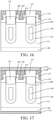
- a continuous self-aligned etching masking layer 116 may be formed on the second isolation dielectric layer 112 and the source 115 around the second isolation dielectric layer 112 by using a chemical vapor deposition process or the like, as shown in Fig. 12 .
- a material of the self-aligned etching masking layer 116 may be silicon oxide or silicon nitride, but is not limited thereto.
- the self-aligned etching masking layer 116 is etched to expose the source 115, to form spacers 117 located on two sides of the second isolation dielectric layer 112 and located on the source 115 around the second isolation dielectric layer 112, as shown in Fig. 13 .
- the self-aligned etching masking layer may be directly etched by using an anisotropic dry etching process without preparing a mask, and the second isolation dielectric layer 112 or the source 115 is used as a detected object at an etching endpoint, so that an upper surface of the source 115 is exposed, and two spacers 117 having a spacing are formed between adjacent second isolation dielectric layers 112, that is, the spacers 117 are formed on two sides of the U-shaped opening.
- the spacer 117 is used as a barrier layer for etching the source contact hole 118 without preparing a masking layer and without being limited by a traditional photolithography process, thereby further reducing a device cell pitch, improving a cell density, and reducing a device channel resistance.
- a size of the source contact hole 118 depends on only a size of the U-shaped opening and a target thickness of the self-aligned etching masking layer 116, but the U-shaped opening is also formed by a self-alignment process, and the size of the formed source contact hole 118 is stable and controllable.
- it is required to maintain a safety distance between the bottom of the source contact hole 118 and the channel, as shown in d in Fig.
- the self-alignment technology is adopted, which is conducive to implementing accurate alignment, to cause the size required by the device structure to be easy to control, thereby improving the stability of the device electrical parameter, and obtaining a device structure with a small cell size, a high cell density, a low device channel resistance, a low specific on-resistance, and a stable electrical parameter.
- an upper surface of the etched epitaxial layer 113 is higher than the upper surface of the gate layer 110 and is lower than an upper surface of the second isolation dielectric layer 112.
- a lower surface of the body region 114 formed by performing ion implantation is higher than a lower surface of the gate layer 110
- a lower surface of the formed source 115 is lower than the upper surface of the gate layer 110.
- the formed source contact hole 118 further extends into the body region 114.
- a distance between the bottom of the source contact hole 118 and the upper surface the body region 114 is between 3 KA and 6 KA, which may be 4.5 KA or 5.5 KA.
- the method further includes the following step: performing ion implantation on the body region 114 based on the source contact hole 118, to form a doping contact region 119 in the body region 114, where a doping type of the doping contact region 119 is consistent with the doping type of the body region 114, and the doping contact region 119 is in contact with the source electrode structure 122.
- Ion implantation is performed on the body region 114 by using an ion implantation process.
- ion implantation is performed based on the source contact hole 118, and the doping type of the doping contact region 119 is consistent with the doping type of the body region 114.
- a doping concentration of the doping contact region 119 is greater than a doping concentration of the body region 114.
- P+ type doped is selected, to reduce a contact resistance.
- a source electrode structure 122 electrically connected to both the source 115 and the body region 114 is formed in at least the source contact hole 118, and a drain electrode structure 123 electrically connected to the substrate 100 is formed on one side of the substrate 100 away from the epitaxial layer 101.
- the source electrode structure 122 fills at least the source contact hole 118 and is electrically connected to both the source 115 and the body region 114, so that the source and the body region may be electrically lead out.
- the source electrode structure 122 includes a plurality of filling portions 120 and a cover portion 121 covering the filling portions 120.
- the filling portion 120 fills at least the source contact hole 118, and an upper surface of the filling portion 120 is not higher than the upper surface of the second isolation dielectric layer 112, the filling portion 120 and the source contact hole 118 are in one-to-one correspondence.
- the filling portion 120 is electrically connected to the source 115 and the body region 114.
- the cover portion 121 covers the filling portions 120, to electrically lead out the filling portions 120.
- the cover portion 121 further extends to cover the second isolation dielectric layer 112 around the filling portion 120.
- a material of the filling portion 120 may be metallic tungsten, aluminum, titanium, or the like, or may be highly doped polysilicon.
- metallic titanium, titanium nitride, and tungsten may be alternatively deposited sequentially. Tungsten, titanium nitride, and titanium are sequentially dry-etched or wet-etched to a target depth to form the filling portion 120, which is not limited thereto.
- the cover portion 121 and the drain electrode structure 123 are deposited again, and the materials of the cover portion 121 and the drain electrode structure 123 may be selected as a conductive metal.
- the method further includes a step of removing the spacers 117.
- the spacers 117 may be removed by using a dry etching process or a wet etching process.
- the source electrode structure 122 fills the source contact hole 118 and further extends onto at least the source 115 around the source contact hole 118 between the adj acent second isolation dielectric layers 112, that is, the source electrode structure 122 forms a T-shaped contact structure.
- the filling portion 120 is the T-shaped contact structure
- the T-shaped contact structure increases a contact area of the source 115 and the body region 114, thereby effectively reducing a contact resistance of the source 115 and increasing an avalanche energy of the device.
- the present disclosure further provides a trench field effect transistor structure.
- the trench field effect transistor structure is preferably manufactured by using the manufacturing method consistent with the present disclosure, or certainly may be manufactured by using another method, which is not limited to thereto.
- the trench field effect transistor structure includes: a substrate 100, an epitaxial layer 101, a device trench 102 formed in the epitaxial layer 101, a shielding dielectric layer 107, a shielding gate layer 105, a first isolation dielectric layer 108, a gate dielectric layer 109, a gate layer 110, a second isolation dielectric layer 112, a body region 114, a source 115, a source contact hole 118 formed in the source 115 and exposing the body region 114, a source electrode structure 122, and a drain electrode structure 123.
- the substrate 100 has a first doping type, and the first doping type (that is, a first conductivity type) may be P-type doping or N-type doping.
- the substrate may be a heavily doped substrate, for example, concentrations of first doping type ions doped in the substrate 100 may be greater than or equal to 1 ⁇ 10 19 /cm 3 .
- the substrate 100 may be a silicon substrate, a germanium silicon substrate, a silicon carbide substrate, or the like.
- the substrate 100 is an N ++ -type doped silicon substrate such as 0.001-0.003 ohm ⁇ cm.
- the epitaxial layer 101 is formed on the substrate 100 and has the first doping type. In an example, a doping concentration of the epitaxial layer 101 is less than that of the substrate 100.
- the epitaxial layer 101 is an N-type monocrystalline silicon epitaxial layer 101.
- a plurality of device trenches 102 are formed in the epitaxial layer 101, and a quantity of device trenches 102 and an arrangement relationship between the device trenches are set according to an actual condition.
- the device trenches may be a plurality of strip-shaped device trenches 102 arranged in parallel at intervals.
- the epitaxial layer 101 is the epitaxial layer 101 obtained by etching in the manufacturing method for a trench field effect transistor structure according to this embodiment.
- the epitaxial layer 101 may be two or more stacked material layers with different concentrations of doping, and a quantity of material layers and a doping concentration of each material layer may be selected according to an actual requirement.
- a position of the device trench 102 may be selected according to an actual requirement, and a specific resistance of the device may be improved based on the setting.
- the epitaxial layer 101 includes two material layers, the bottom of the device trench 102 is stopped on the upper material layer, that is, at a junction of the two material layers, and the device trench exposes the lower material layer.
- the shielding dielectric layer 107 is formed on the bottom and a part of side walls of the device trench 102.
- a material of the shielding dielectric layer 107 may include, but is not limited to, silicon oxide.
- a thickness of the shielding dielectric layer 107 may be between 800A and 9000A, for example, may be 1000A, 2000A, or 8000A, to achieve a good shielding effect.
- the shielding gate layer 105 is formed on a surface of the shielding dielectric layer 107 and fills at least the bottom of the device trench 102, and a material of the shielding gate layer 105 may include, but is not limited to, polysilicon.
- the first isolation dielectric layer 108 is formed on the shielding gate layer 105, the first isolation dielectric layer 108 and the shielding dielectric layer 107 surround the shielding gate layer 105, and a material of the first isolation dielectric layer 108 includes, but is not limited to, a high-density plasma (HDP) oxide layer.
- a high-density plasma (HDP) oxide layer includes, but is not limited to, a high-density plasma (HDP) oxide layer.
- HDP high-density plasma
- an upper surface of the first isolation dielectric layer 108 is flush with an upper surface of the shielding dielectric layer 107, and a height of the first isolation dielectric layer 108 is between 1500A and 4500A, for example, may be 2000A or 3000A.
- the gate dielectric layer is formed on a surface of the first isolation dielectric layer 108 and extends onto the upper surface of the shielding dielectric layer 107 and the inner wall of the device trench 102, and a gate trench is defined by the surface of the gate dielectric layer 109.
- the gate dielectric layer 109 may be a silicon oxide layer or a high dielectric constant dielectric layer, but is not limited thereto.
- the gate layer 110 fills the gate trench, and an upper surface of the gate layer 110 is lower than an upper surface of the epitaxial layer 101.
- a material of the gate layer 110 includes, but is not limited to, polysilicon.
- the second isolation dielectric layer 112 is formed on the gate layer 110 and covers at least an exposed surface of the gate layer 110, and the second isolation dielectric layer 112 and the gate dielectric layer 109 surround the gate layer 110.
- a material of the second isolation dielectric layer 112 includes, but is not limited to, silicon oxide.
- the second isolation dielectric layer 112 is higher than the upper surface of the epitaxial layer 101.
- the body region 114 of the second doping type is formed in the epitaxial layer 101 between adjacent device trenches 102 and abuts the adjacent device trenches 102.
- the second doping type is a P-type
- a P-doped body region 114 is selected for the body region 114
- the source 115 is formed in the body region 114 and has the first doping type
- an ion doping type of the source 115 is the same as the doping types of the epitaxial layer 101 and the substrate 100, and is opposite to the doping type of the body region 114.
- an N+ type doped silicon is selected for the source 115.
- the source contact hole 118 that runs through the source 115 and exposes the body region 114 is formed in the source 115. In an example, the source contact hole 118 further extends into the body region 114.
- the source electrode structure 122 fills at least the source contact hole 118 and is electrically connected to both the source 115 and the body region 114, and the drain electrode structure 123 is formed on one side of the substrate 100 away from the epitaxial layer 101 and is electrically connected to the substrate 100.
- the source electrode structure 122 is electrically connected to both the source 115 and the body region 114, so that the source and the body region may be electrically lead out.
- the source electrode structure 122 includes a plurality of filling portions 120 and a cover portion 121 covering the filling portions 120.
- the filling portion 120 fills at least the source contact hole 118, and an upper surface of the filling portion 120 is not higher than the upper surface of the second isolation dielectric layer 112, the filling portion 120 and the source contact hole 118 are in one-to-one correspondence, the filling portion 120 is electrically connected to the source 115 and the body region 114, the cover portion 121 covers the filling portions 120, to electrically lead out the filling portions 120, and the cover portion 121 further extends to cover the second isolation dielectric layer 112 around the filling portion 120.
- a material of the filling portion 120 may be metallic tungsten, aluminum, titanium, or the like, or may be highly doped polysilicon.
- metallic titanium, titanium nitride, and tungsten may be alternatively deposited sequentially.
- Tungsten, titanium nitride, and titanium are sequentially dry-etched or wet-etched to a target depth to form the filling portion 120, which is not limited thereto.
- the cover portion 121 and the drain electrode structure 123 are then deposited, and the materials of the cover portion 121 and the drain electrode structure 123 may be a conductive metal.
- the upper surface of the epitaxial layer 101 is higher than the upper surface of the gate layer 110 and is lower than the upper surface of the second isolation dielectric layer 112, and the source electrode structure 122 fills the source contact hole 118 and further extends onto at least the source 115 around the source contact hole 118 between the adjacent second isolation dielectric layers 112, that is, the source electrode structure 122 forms a T-shaped contact structure.
- the source 115 includes the filling portion 120 and the cover portion 121
- the filling portion 120 is the T-shaped contact structure
- the T-shaped contact structure increases a contact area of the source 115 and the body region 114, thereby effectively reducing a contact resistance of the source 115 and increasing an avalanche energy of the device.
- the trench field effect transistor structure further includes spacers 117 formed on two sides of the second isolation dielectric layer 112 and located at the source 115 around the second isolation dielectric layer 112.
- the trench field effect transistor structure further includes a doping contact region 119, a doping type of the doping contact region 119 is the same as the doping type of the body region 114, and the doping contact region 119 is in contact with the source electrode structure 122.
- a doping concentration of the doping contact region 119 is greater than a doping concentration of the body region 114.
- P+ type doped is selected, to reduce a contact resistance.
- a lower surface of the body region 114 is higher than a lower surface of the gate layer 110
- a lower surface of the source 115 is lower than the upper surface of the gate layer 110
- the source contact hole 118 is formed in the source 115 and further extends into the body region 114.
- the present disclosure provides a trench field effect transistor structure and a manufacturing method, a self-alignment process is adopted in a manufacturing process, so that a cell unit pitch is not limited by an exposure capability and alignment accuracy of a lithography machine, to further reduce the cell unit pitch of a device, improve a cell density, and reduce a device channel resistance, so that a device structure with a stable electrical parameter and a low specific on-resistance is obtained.
- a source electrode structure of a "T"-shaped structure is disposed, to increase a contact area between the source electrode structure and a source and a contact area between the source electrode structure and a body region, thereby effectively reducing a source contact resistance and improving an avalanche tolerance of the device. Therefore, the present disclosure effectively overcomes various defects in the prior art, and has a high value in industrial use.
Landscapes
- Electrodes Of Semiconductors (AREA)
- Insulated Gate Type Field-Effect Transistor (AREA)
- Engineering & Computer Science (AREA)
- Manufacturing & Machinery (AREA)
- Element Separation (AREA)
Applications Claiming Priority (2)
| Application Number | Priority Date | Filing Date | Title |
|---|---|---|---|
| CN201911192262.1A CN112864018B (zh) | 2019-11-28 | 2019-11-28 | 沟槽型场效应晶体管结构及其制备方法 |
| PCT/CN2019/130511 WO2021103274A1 (fr) | 2019-11-28 | 2019-12-31 | Structure de transistor à effet de champ à tranchée et procédé de préparation correspondant |
Publications (2)
| Publication Number | Publication Date |
|---|---|
| EP3965166A1 true EP3965166A1 (fr) | 2022-03-09 |
| EP3965166A4 EP3965166A4 (fr) | 2023-02-08 |
Family
ID=75995608
Family Applications (1)
| Application Number | Title | Priority Date | Filing Date |
|---|---|---|---|
| EP19954187.1A Pending EP3965166A4 (fr) | 2019-11-28 | 2019-12-31 | Structure de transistor à effet de champ à tranchée et procédé de préparation correspondant |
Country Status (6)
| Country | Link |
|---|---|
| US (1) | US12166109B2 (fr) |
| EP (1) | EP3965166A4 (fr) |
| JP (1) | JP2022523960A (fr) |
| KR (1) | KR102614549B1 (fr) |
| CN (1) | CN112864018B (fr) |
| WO (1) | WO2021103274A1 (fr) |
Families Citing this family (20)
| Publication number | Priority date | Publication date | Assignee | Title |
|---|---|---|---|---|
| US11848378B2 (en) * | 2020-08-13 | 2023-12-19 | Stmicroelectronics Pte Ltd | Split-gate trench power MOSFET with self-aligned poly-to-poly isolation |
| CN113270321A (zh) * | 2021-07-01 | 2021-08-17 | 安建科技(深圳)有限公司 | 一种高密度屏蔽栅沟槽型场效应管器件的制造方法 |
| CN113725300B (zh) * | 2021-08-30 | 2022-04-26 | 深圳真茂佳半导体有限公司 | 多源mos管共用栅极的芯片结构及其制造方法 |
| CN113964038B (zh) * | 2021-09-24 | 2023-06-23 | 杭州芯迈半导体技术有限公司 | 沟槽栅mosfet器件的制造方法 |
| CN114420637B (zh) * | 2021-12-22 | 2023-12-29 | 深圳深爱半导体股份有限公司 | 半导体器件结构及其制备方法 |
| CN114068683B (zh) * | 2022-01-17 | 2022-04-22 | 深圳市威兆半导体有限公司 | 屏蔽栅极金氧半场效晶体管元胞结构、晶体管及制造方法 |
| CN114242596A (zh) * | 2022-02-28 | 2022-03-25 | 深圳市美浦森半导体有限公司 | 一种mosfet器件及其制造方法 |
| CN114566542B (zh) * | 2022-03-01 | 2026-03-06 | 绍兴中芯集成电路制造股份有限公司 | 屏蔽栅沟槽型场效应晶体管及其制作方法 |
| US12482706B2 (en) * | 2022-07-12 | 2025-11-25 | Vanguard International Semiconductor Corporation | Semiconductor structure that includes self-aligned contact plugs and methods for manufacturing the same |
| CN115312392B (zh) * | 2022-07-28 | 2025-06-10 | 上海华虹宏力半导体制造有限公司 | 栅介质层的形成方法 |
| CN115528102B (zh) * | 2022-10-09 | 2026-01-13 | 苏州聚谦半导体有限公司 | 自对准双槽屏蔽栅igbt结构及其制造方法 |
| CN115831732B (zh) * | 2022-11-28 | 2025-11-25 | 上海鼎泰匠芯科技有限公司 | 半导体结构的制备方法 |
| CN115966538A (zh) * | 2022-12-16 | 2023-04-14 | 黄山芯微电子股份有限公司 | 一种功率器件元胞结构的接触孔结构及其制造方法 |
| CN116110851A (zh) * | 2022-12-29 | 2023-05-12 | 瑶芯微电子科技(上海)有限公司 | 一种屏蔽栅沟槽场效应晶体管结构及其制作方法 |
| CN116093133A (zh) * | 2023-01-28 | 2023-05-09 | 上海鼎泰匠芯科技有限公司 | 半导体结构及其制备方法 |
| CN116246961A (zh) * | 2023-04-12 | 2023-06-09 | 上海鼎泰匠芯科技有限公司 | 半导体结构的制备方法及半导体结构 |
| CN116190451B (zh) * | 2023-04-18 | 2024-05-03 | 杭州芯迈半导体技术有限公司 | 栅源结构及制造方法、非对称沟槽型mosfet及制造方法 |
| EP4478420A1 (fr) * | 2023-06-14 | 2024-12-18 | Nexperia B.V. | Mosfet à grille divisée |
| TWI868962B (zh) * | 2023-10-03 | 2025-01-01 | 世界先進積體電路股份有限公司 | 半導體裝置及其製造方法 |
| CN117747433B (zh) * | 2023-12-25 | 2024-10-22 | 深圳芯能半导体技术有限公司 | 一种沟槽栅型功率器件及其制备方法、元胞版图结构 |
Family Cites Families (21)
| Publication number | Priority date | Publication date | Assignee | Title |
|---|---|---|---|---|
| JP2006202931A (ja) * | 2005-01-20 | 2006-08-03 | Renesas Technology Corp | 半導体装置およびその製造方法 |
| US7385248B2 (en) * | 2005-08-09 | 2008-06-10 | Fairchild Semiconductor Corporation | Shielded gate field effect transistor with improved inter-poly dielectric |
| US9947770B2 (en) * | 2007-04-03 | 2018-04-17 | Vishay-Siliconix | Self-aligned trench MOSFET and method of manufacture |
| US7799642B2 (en) * | 2007-10-02 | 2010-09-21 | Inpower Semiconductor Co., Ltd. | Trench MOSFET and method of manufacture utilizing two masks |
| US8686493B2 (en) * | 2007-10-04 | 2014-04-01 | Fairchild Semiconductor Corporation | High density FET with integrated Schottky |
| US8362548B2 (en) * | 2008-11-14 | 2013-01-29 | Semiconductor Components Industries, Llc | Contact structure for semiconductor device having trench shield electrode and method |
| US7952141B2 (en) * | 2009-07-24 | 2011-05-31 | Fairchild Semiconductor Corporation | Shield contacts in a shielded gate MOSFET |
| US8779510B2 (en) * | 2010-06-01 | 2014-07-15 | Alpha And Omega Semiconductor Incorporated | Semiconductor power devices manufactured with self-aligned processes and more reliable electrical contacts |
| US8829603B2 (en) * | 2011-08-18 | 2014-09-09 | Alpha And Omega Semiconductor Incorporated | Shielded gate trench MOSFET package |
| US8642425B2 (en) * | 2012-05-29 | 2014-02-04 | Semiconductor Components Industries, Llc | Method of making an insulated gate semiconductor device and structure |
| US20140273374A1 (en) * | 2013-03-15 | 2014-09-18 | Joseph Yedinak | Vertical Doping and Capacitive Balancing for Power Semiconductor Devices |
| JP6170812B2 (ja) * | 2013-03-19 | 2017-07-26 | 株式会社東芝 | 半導体装置の製造方法 |
| US9281368B1 (en) * | 2014-12-12 | 2016-03-08 | Alpha And Omega Semiconductor Incorporated | Split-gate trench power MOSFET with protected shield oxide |
| US10020380B2 (en) * | 2015-01-23 | 2018-07-10 | Alpha And Omega Semiconductor Incorporated | Power device with high aspect ratio trench contacts and submicron pitches between trenches |
| CN108257869A (zh) * | 2016-12-28 | 2018-07-06 | 中航(重庆)微电子有限公司 | 屏蔽栅沟槽mosfet的制备方法 |
| CN106847880B (zh) * | 2017-01-23 | 2019-11-26 | 矽力杰半导体技术(杭州)有限公司 | 一种半导体器件及其制备方法 |
| CN107871787B (zh) | 2017-10-11 | 2021-10-12 | 矽力杰半导体技术(杭州)有限公司 | 一种制造沟槽mosfet的方法 |
| JP2019129300A (ja) * | 2018-01-26 | 2019-08-01 | トヨタ自動車株式会社 | 半導体装置とその製造方法 |
| US10777661B2 (en) * | 2018-03-01 | 2020-09-15 | Ipower Semiconductor | Method of manufacturing shielded gate trench MOSFET devices |
| JP6918736B2 (ja) * | 2018-04-02 | 2021-08-11 | 株式会社豊田中央研究所 | 半導体装置 |
| TWI684276B (zh) * | 2019-01-11 | 2020-02-01 | 力源半導體股份有限公司 | 溝渠式功率電晶體及其製作方法 |
-
2019
- 2019-11-28 CN CN201911192262.1A patent/CN112864018B/zh active Active
- 2019-12-31 JP JP2021552502A patent/JP2022523960A/ja active Pending
- 2019-12-31 WO PCT/CN2019/130511 patent/WO2021103274A1/fr not_active Ceased
- 2019-12-31 KR KR1020217026141A patent/KR102614549B1/ko active Active
- 2019-12-31 US US17/616,464 patent/US12166109B2/en active Active
- 2019-12-31 EP EP19954187.1A patent/EP3965166A4/fr active Pending
Also Published As
| Publication number | Publication date |
|---|---|
| EP3965166A4 (fr) | 2023-02-08 |
| WO2021103274A1 (fr) | 2021-06-03 |
| CN112864018A (zh) | 2021-05-28 |
| CN112864018B (zh) | 2022-07-19 |
| US20220328658A1 (en) | 2022-10-13 |
| JP2022523960A (ja) | 2022-04-27 |
| US12166109B2 (en) | 2024-12-10 |
| KR20210115016A (ko) | 2021-09-24 |
| KR102614549B1 (ko) | 2023-12-14 |
Similar Documents
| Publication | Publication Date | Title |
|---|---|---|
| US12166109B2 (en) | Trench field effect transistor structure comprising epitaxial layer and manufacturing method thereof | |
| US11075297B2 (en) | Semiconductor device and method of manufacturing semiconductor device | |
| US6765264B1 (en) | Method of fabricating power rectifier device to vary operating parameters and resulting device | |
| US20130153995A1 (en) | Semiconductor device and method for manufacturing the same | |
| WO2021068420A1 (fr) | Structure de transistor à effet de champ de type à tranchées et son procédé de préparation | |
| US6528355B2 (en) | Method for fabricating a trench MOS power transistor | |
| CN105448732B (zh) | 改善uis性能的沟槽式功率半导体器件及其制备方法 | |
| CN115241283B (zh) | 集成的平面-沟道栅极功率mosfet | |
| WO2021082273A1 (fr) | Structure de transistor à effet de champ de type à tranchées et son procédé de préparation | |
| KR20030023718A (ko) | 종형 전력 트랜지스터 트렌치 게이트 반도체 디바이스제조 방법 | |
| CN104103693A (zh) | 一种u形沟槽的功率器件及其制造方法 | |
| CN107731926B (zh) | 提高耐压范围的mosfet器件及其制备方法 | |
| CN115424939A (zh) | 一种沟槽型mosfet及其制备方法 | |
| US11652170B2 (en) | Trench field effect transistor structure free from contact hole | |
| CN108231900A (zh) | 一种功率半导体器件及其制备方法 | |
| CN115312601A (zh) | Mosfet器件及其制备方法 | |
| CN117690795A (zh) | 一种新型屏蔽栅沟槽场效应晶体管及其制备方法 | |
| CN107658342B (zh) | 非对称的屏蔽栅mosfet结构及其制备方法 | |
| CN216389378U (zh) | 一种沟槽型功率器件 | |
| CN111933700A (zh) | 功率半导体器件及其制造方法 | |
| WO2023178895A1 (fr) | Procédé de fabrication d'un dispositif en carbure de silicium | |
| WO2023178866A1 (fr) | Dispositif en carbure de silicium et son procédé de fabrication | |
| CN121531775A (zh) | 半导体结构及其形成方法 | |
| CN113284953A (zh) | 一种屏蔽栅沟槽型mosfet结构及其制造方法 | |
| CN119170636A (zh) | 一种半导体器件及其制备方法 |
Legal Events
| Date | Code | Title | Description |
|---|---|---|---|
| STAA | Information on the status of an ep patent application or granted ep patent |
Free format text: STATUS: THE INTERNATIONAL PUBLICATION HAS BEEN MADE |
|
| PUAI | Public reference made under article 153(3) epc to a published international application that has entered the european phase |
Free format text: ORIGINAL CODE: 0009012 |
|
| STAA | Information on the status of an ep patent application or granted ep patent |
Free format text: STATUS: REQUEST FOR EXAMINATION WAS MADE |
|
| 17P | Request for examination filed |
Effective date: 20211203 |
|
| AK | Designated contracting states |
Kind code of ref document: A1 Designated state(s): AL AT BE BG CH CY CZ DE DK EE ES FI FR GB GR HR HU IE IS IT LI LT LU LV MC MK MT NL NO PL PT RO RS SE SI SK SM TR |
|
| REG | Reference to a national code |
Ref country code: DE Ref legal event code: R079 Free format text: PREVIOUS MAIN CLASS: H01L0029739000 Ipc: H01L0021336000 |
|
| A4 | Supplementary search report drawn up and despatched |
Effective date: 20230109 |
|
| RIC1 | Information provided on ipc code assigned before grant |
Ipc: H01L 29/78 19740701ALI20230102BHEP Ipc: H01L 21/336 19900101AFI20230102BHEP |
|
| DAV | Request for validation of the european patent (deleted) | ||
| DAX | Request for extension of the european patent (deleted) |