EP3942222B1 - Led-glühlampe und herstellungsverfahren dafür - Google Patents
Led-glühlampe und herstellungsverfahren dafür Download PDFInfo
- Publication number
- EP3942222B1 EP3942222B1 EP20710524.8A EP20710524A EP3942222B1 EP 3942222 B1 EP3942222 B1 EP 3942222B1 EP 20710524 A EP20710524 A EP 20710524A EP 3942222 B1 EP3942222 B1 EP 3942222B1
- Authority
- EP
- European Patent Office
- Prior art keywords
- wire
- envelope
- stem portion
- lighting driver
- lighting
- Prior art date
- Legal status (The legal status is an assumption and is not a legal conclusion. Google has not performed a legal analysis and makes no representation as to the accuracy of the status listed.)
- Active
Links
Images



Classifications
-
- F—MECHANICAL ENGINEERING; LIGHTING; HEATING; WEAPONS; BLASTING
- F21—LIGHTING
- F21K—NON-ELECTRIC LIGHT SOURCES USING LUMINESCENCE; LIGHT SOURCES USING ELECTROCHEMILUMINESCENCE; LIGHT SOURCES USING CHARGES OF COMBUSTIBLE MATERIAL; LIGHT SOURCES USING SEMICONDUCTOR DEVICES AS LIGHT-GENERATING ELEMENTS; LIGHT SOURCES NOT OTHERWISE PROVIDED FOR
- F21K9/00—Light sources using semiconductor devices as light-generating elements, e.g. using light-emitting diodes [LED] or lasers
- F21K9/20—Light sources comprising attachment means
- F21K9/23—Retrofit light sources for lighting devices with a single fitting for each light source, e.g. for substitution of incandescent lamps with bayonet or threaded fittings
- F21K9/232—Retrofit light sources for lighting devices with a single fitting for each light source, e.g. for substitution of incandescent lamps with bayonet or threaded fittings specially adapted for generating an essentially omnidirectional light distribution, e.g. with a glass bulb
-
- F—MECHANICAL ENGINEERING; LIGHTING; HEATING; WEAPONS; BLASTING
- F21—LIGHTING
- F21V—FUNCTIONAL FEATURES OR DETAILS OF LIGHTING DEVICES OR SYSTEMS THEREOF; STRUCTURAL COMBINATIONS OF LIGHTING DEVICES WITH OTHER ARTICLES, NOT OTHERWISE PROVIDED FOR
- F21V23/00—Arrangement of electric circuit elements in or on lighting devices
- F21V23/001—Arrangement of electric circuit elements in or on lighting devices the elements being electrical wires or cables
- F21V23/002—Arrangements of cables or conductors inside a lighting device, e.g. means for guiding along parts of the housing or in a pivoting arm
-
- F—MECHANICAL ENGINEERING; LIGHTING; HEATING; WEAPONS; BLASTING
- F21—LIGHTING
- F21K—NON-ELECTRIC LIGHT SOURCES USING LUMINESCENCE; LIGHT SOURCES USING ELECTROCHEMILUMINESCENCE; LIGHT SOURCES USING CHARGES OF COMBUSTIBLE MATERIAL; LIGHT SOURCES USING SEMICONDUCTOR DEVICES AS LIGHT-GENERATING ELEMENTS; LIGHT SOURCES NOT OTHERWISE PROVIDED FOR
- F21K9/00—Light sources using semiconductor devices as light-generating elements, e.g. using light-emitting diodes [LED] or lasers
- F21K9/20—Light sources comprising attachment means
- F21K9/23—Retrofit light sources for lighting devices with a single fitting for each light source, e.g. for substitution of incandescent lamps with bayonet or threaded fittings
- F21K9/238—Arrangement or mounting of circuit elements integrated in the light source
-
- F—MECHANICAL ENGINEERING; LIGHTING; HEATING; WEAPONS; BLASTING
- F21—LIGHTING
- F21K—NON-ELECTRIC LIGHT SOURCES USING LUMINESCENCE; LIGHT SOURCES USING ELECTROCHEMILUMINESCENCE; LIGHT SOURCES USING CHARGES OF COMBUSTIBLE MATERIAL; LIGHT SOURCES USING SEMICONDUCTOR DEVICES AS LIGHT-GENERATING ELEMENTS; LIGHT SOURCES NOT OTHERWISE PROVIDED FOR
- F21K9/00—Light sources using semiconductor devices as light-generating elements, e.g. using light-emitting diodes [LED] or lasers
- F21K9/90—Methods of manufacture
Definitions
- This invention relates to a LED lighting bulb and manufacturing method, and in particular to a bulb which incorporates a lighting driver.
- a LED lighting bulb in particular which is able to be driven by mains power, requires a lighting driver circuit to be incorporated into the bulb.
- the lighting driver may for example be a switch mode power converter or other type of driver circuit.
- a LED lighting bulb typically comprises a glass envelope and an end cap which closes an opening in the glass envelope and defines the external terminal contacts of the bulb.
- the end cap may be an Edison screw fitting (e.g. E17 or E27) or a bayonet cap (e.g. B15 or B22) or a pin connector (e.g. MR16).
- the end cap is located outside the envelope and for example has (or is attached to) a stem which seals the opening in the envelope.
- the known approach is to position the lighting driver in the end cap.
- the stem of the end cap can be sealed to the glass envelope before the lighting driver is connected.
- Assembly of the end cap is then involves connecting the lighting driver and connecting the terminals of the end cap to the lighting driver.
- the end cap may be deliberately enlarged to provide additional internal space for the lighting driver. This detracts from the aesthetic appearance of the bulb and also adds to the overall size of the bulb which may not be desired.
- WO2016/145923A1 , CN103225757B , US2013/0271989A1 and US2010/0253221 A1 disclose different structures of LED bulbs. However, above problem is not mentioned or solved.
- a LED lighting bulb comprising:
- This bulb has a lighting driver on the envelope side of the stem portion of the end cap, i.e. within the bulb envelope.
- the lighting driver is slideable along the first and second wires. This means the assembly can take place with the lighting driver remote from the stem portion, and after assembly, the lighting driver can be pulled back to the stem portion using the first and second supply wires.
- the lighting driver is able to slide along (or over or between) the first wire and the second wire.
- the lighting driver can be positioned within the interior volume of the envelope, and does not need to be confined to an internal volume of the end cap.
- an uncluttered internal volume also avoids shadowing, which could result if the driver is located within the envelope near to the light source (e.g. LED filament) and thereby block some of the LED light, creating shadows in the output light. It also means the positioning of the light source can be freely selected, even for different sizes of driver.
- the light source e.g. LED filament
- the first supply wire is preferably sealed within the first tube and the second supply wire is preferably sealed within the second tube.
- This provides a firm fixing for the wires within the tubes.
- the tubes may be sintered around the wires to provide a firm fixing. This enables robust electrical connections to be made.
- the tubes are thus used to form a seal around their respective supply wires.
- the tubes can be for example be used for evacuating the envelope or filling the envelope with a gas after the envelope and stem portion have been connected.
- the shape feature comprises a first through hole around the first wire and a second through hole around the second wire. In another example, the shape feature comprises a first slot around the first wire and a second slot around the second wire.
- These holes or slots allow the lighting driver to slide over the first and second wires, and this provides positioning of the lighting driver during this sliding operation. They enable the lighting driver to be as large as the stem portion (in a plane perpendicular to the sliding direction). An alternative is for the lighting driver to slide between the first and second wires, but this will limit further the possible size of the lighting driver.
- the first and second wires may still perform a centering function by which the position of the driver is approximately defined (i.e. between the first and second wires), while it is pulled back towards the stem portion. After the driver has been pulled back to the stem portion, the relative positioning between the stem portion and the driver becomes fixed because the positions of the supply wires relative to the stem portion are then fixed, in particular at the locations of openings through the stem portion.
- Any other suitable guiding arrangement may be used to define the path of the lighting driver between the remote position (before pulling back) and the pulled back position against the stem portion.
- the lighting driver comprises an anode output wire and a cathode output wire which are soldered to the first wire and second wire respectively. This soldered connection may take place as part of the process of also connecting an LED arrangement between the first wire and the second wire.
- the holes or slots may be electrically connected to output terminals of the lighting driver.
- they may be formed in a printed circuit board, for example comprising conducting vias.
- the output terminals of the lighting driver are then connected the first and second wires by electrical contact between the first and second wires and the holes or slots.
- soldered electrical connections to the driver may be provided, or else by positioning the lighting driver in place, for example abutted against the stem portion, the electrical connections between the first and second wires to output terminals of the lighting driver may be automatically ensured.
- the envelope is preferably glass, and the stem portion is sintered to the envelope. During this sintering, the lighting driver can be positioned at a remote location from the stem, further into the envelope.
- the first and second tubes are for example also glass and they are each sintered around their respective supply wire. This provides the thermal sealing of the envelope.
- the lighting driver can be in place next to the stem during this process despite the high temperature, because the tubes are on the opposite side of the stem portion to the lighting driver so the lighting driver is protected by the stem portion.
- the stem portion is for example also formed of glass.
- the end cap for example further comprises a terminal portion which defines the first and second terminals.
- the assembly of the terminal portion to the stem portion is the final assembly stage.
- the LED arrangement is preferably connected between the first wire and the second wire. This connection is made after the lighting driver is mounted over the first and second wires, but before the stem portion is attached to the envelope.
- the invention also provides a method of manufacturing a LED lighting bulb comprising:
- This method enables a lighting driver to be positioned inside the bulb envelope and at a safe distance from the stem portion when the stem portion is attached to the envelope.
- the lighting driver can then be pulled into position using the supply wires. It may for example be pulled against the stem portion, so that it occupies a specific position abutted against the stem portion, but on the envelope side of the stem portion, i.e. within the bulb envelope rather than within the end cap.
- connection of the lighting driver to the first and second wires may take place automatically by pulling the lighting driver into position.
- the envelope and the tubes are for example glass, and the hermetically connecting step and the sealing step comprise sintering.
- the sintering is a high temperature process, and the method avoids thermal damage to the lighting driver, which is already installed when the sintering takes place, because it is to be mounted inside the envelope.
- the method may further comprise evacuating the envelope or filling the envelope with a gas before sealing the tubes around the first and second supply wires.
- Pulling the lighting driver towards the stem portion using the first and second supply wires for example comprises pulling the lighting driver to slide relative to the first wire and the second wire along a shape feature of the lighting driver.
- the method may further comprise connecting the lighting driver to the first and second wires by soldering before hermetically connecting the stem portion to the opening of the envelope (and indeed before the pulling step).
- the shape feature for example comprises a first through hole or slot around the first wire and a second through hole or slot around the second wire
- the method comprises connecting the lighting driver to the first and second wires by electrically connecting the holes or slots to output terminals of the lighting driver during the step of pulling.
- the holes or slots for example have conductive inner surfaces which make electrical contact with the first or second wires.
- the method may further comprise connecting the LED arrangement between the first wire and the second wire before hermetically connecting the stem portion to the opening of the envelope.
- the invention provides a LED lighting bulb in which a lighting driver is located within the bulb envelope.
- the lighting driver may be positioned away from an opening of the envelope so that high temperature sealing of a stem portion of the end cap to the envelope opening can take place. The lighting driver can then be pulled into position against the stem portion, and assembly of the end cap can then be completed.
- Figure 1 shows a known LED bulb 10 comprising an envelope 12 having an opening 14.
- An end cap 16 is at the opening.
- the end cap defines the external electrical connector for connection to a bulb holder.
- the end cap 16 Within the volume of the end cap 16 is a lighting driver. To make space for the lighting driver in the end cap volume, outside the envelope 12 of the bulb, the end cap comprises a standard connector part 16a (such as a screw fitting as shown) and also an additional volume 16b.
- a standard connector part 16a such as a screw fitting as shown
- this additional volume 16b is normally enclosed by a non-transparent material, such as a metal/plastic over-molding housing, it changes the appearance of the bulb and may not be desired. It would be preferred to enable the connector to be as small as possible and to house the lighting driver in the envelope.
- FIG. 2 shows a bulb in accordance with an example of the invention.
- the LED bulb 10 again comprising an envelope 12 in a bulbous shape, for example of glass, having an opening 14, and an end cap 16 at the opening.
- the end cap 16 has an electrical connector part 40 with a first terminal 18 and a second terminal 20 for making electrical connection with a bulb holder.
- the end cap further comprises a stem portion 22 which closes the opening in the envelope.
- a first wire 24 and a second wire 26 extend from the stem portion 22 into the envelope.
- the stem portion is the part that closes and therefore seals the envelope volume. It is also a glass component. Note that for the purposes of this description, the stem portion is considered to be part of the end cap. It could equally be considered to be a separate part to which the end cap connects.
- the lighting driver 28 is positioned at an envelope side of the stem portion 22, namely within the envelope volume.
- the lighting driver 28 comprises a shape feature (described further below) for allowing the lighting driver to slide relative to the first wire 24 and the second wire 26, and the lighting driver 28 is electrically connected to the first wire and the second wire.
- This shape feature allows the lighting driver to be located further towards the center of the envelope volume when the stem portion 22 is connected to the envelope. The lighting driver can then be pulled back to the stem portion.
- An LED filament 42 is provided between the first wire and the second wire. This takes the form of one or more light emitting strips.
- the bulb thus has the lighting driver on the envelope side of the stem portion of the end cap, i.e. within the bulb envelope.
- the lighting driver is slideable along the first and second wires.
- Figure 3 shows the stem portion 22, with the first wire 24 and second wire 26 projecting from a first side, in particular the envelope side (i.e. the side or end of the stem portion 22 which faces into the envelope volume when the bulb is assembled).
- the opposite side of the stem portion may be considered to be an end cap side.
- a tube arrangement 34 comprising a first glass tube 34a and a second glass tube 34b.
- Figure 4 shows the lighting driver 28 mounted over the first wire 24. In Figure 4 it is shown initially mounted over the first wire 24, but it is then slid down until it also passes over the second wire 26.
- the lighting driver comprises a circuit board 28a and components 28b mounted on the circuit board 28a.
- a driver output anode cable 27a and a driver output cathode cable 27b extend from the circuit board 28a for soldering with the first wire 24 and second wire 26 respectively to provide the electrical output connections from the driver.
- a shape feature is provided for allowing the lighting driver to slide relative to the first wire 24 and the second wire 26.
- This shape feature for example comprises a pair of openings, one opening 30 of which can be seen in Figure 4 which will slide over the second wire 26 when the lighting driver 28 is lowered further towards the stem portion 22.
- openings may instead be radially opening slots.
- a first supply wire 36 extends from the lighting driver 28, through a first opening 23a in the stem portion 22 and through the first tube 34a.
- a second supply wire 38 extends from the lighting driver 28, through a second opening 23b in the stem portion 22 and through the second tube 34b. The first and second supply wires make electrical contact with input terminals of the lighting driver.
- the first supply wire 36 is for making electrical connection between the first terminal 18 and a first input terminal of the lighting driver through the first tube 34a and through the stem portion 22; and the second supply wire 38 is for making electrical connection between the second terminal 20 and a second input terminal of the lighting driver 28 through the second tube 34b and through the stem portion.
- Figure 5 shows the lighting driver 28 mounted over both the first wire 24 and the second wire 26.
- the LED string 42 can then be connected between the first wire and second wire.
- driver output anode cable 27a connects to the first wire at location 29a and the driver output cathode cable 27b connects to the second wire at location 29b. This is by for example soldering. As shown in Figure 5 , there is slack in the cables 27a, 27b so that the driver 28 is free to slide towards the stem portion, which will result in straightening of the cables 27a, 27b.
- Figure 6 shows that the assembly of Figure 5 is then inserted into the bulb envelope 12.
- the stem portion closes the opening of the envelope.
- a sintering process is then used to seal the stem portion to the envelope.
- the lighting driver 28 is positioned spaced apart from the stem portion, as shown. Thus, it is not in contact with the stem portion, but there is an air gap between them. This prevents direct thermal conduction to the lighting driver 28 and protects the lighting driver from the sintering temperature.
- the spacing is for example more than 5mm, for example more than 1 cm.
- Figure 7 shows how the supply wires 36, 38 are then pulled to move the lighting driver 28 towards the stem portion 22, preferably until it makes contact with the stem portion 22.
- the driver output anode cable 27a and the driver output cathode cable 27b are straightened during this process.
- the first supply wire 36 is then is sealed within the first tube 34a and the second supply wire 38 is sealed within the second tube 34b. This is a further sintering process.
- This process provides a hermetic seal to the interior volume of the envelope (and the seal between the stem portion 22 and the opening is also hermetic).
- the tubes may be used to evacuate the envelope volume or to provide a gas such as a gas with a high coefficient of thermal conductivity and low viscosity. Helium or hydrogen or a mixture thereof may be used, and this can reduce the heat sink requirements.
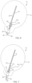
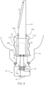
- Figure 8 shows more clearly the electrical connections and shows that the driver inputs 36 and 38 contact with the end cap, whereas the driver output cables 27a and 27b are soldered to the first wire 24 and the second wire 26 at soldering points 29a and 29b.
- the end cap 16 is then assembled. This involves connecting the first supply wire 36 to the first terminal 18 and connecting the second supply wire 38 to the second terminal 20, as shown. The end cap is thereby assembled, by coupling the stem portion 22 and the terminal portion 40.
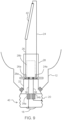
- Figure 9 shows an alternative electrical connection arrangement.
- the first and second wires 24, 26 each comprise a respective enlarged foot portion 24a, 26a.
- the PCB 28a of the lighting driver 28 comprises conductive vias as the openings 30.
- the enlarged foot portions 24a, 26a make electrical contact and frictional engagement with the conductive vias.
- the output of the lighting driver is connected to the first wire and second wire for driving the LED filament in an automatic way without needing additional soldered wires.
- the other features are the same as in Figure 8 .
- any other electrical contact design may be used by which the movement of the lighting driver 28 into its final position results in an electrical connection being made between the lighting driver output terminals and the first and second wires.
- other types of electrical connections may be made such as using electrical connectors.
- Figure 10 shows a method of manufacturing a LED lighting bulb.
- step 50 an envelope is provided having an opening.
- a stem portion of an end cap having a first wire and a second wire extending from the stem portion (shown in Figure 3 ).
- a pair of tubes also extend back from the stem portion on the opposite side to the first and second wires.
- a lighting driver is mounted along the first wire and second wire (shown in Figure 4 ).
- the lighting driver comprises first and second supply wires which extend through the stem portion and each through a respective one of the tubes.
- step 56 an LED arrangement is connected between the first wire and the second wire and, for the design of Figure 8 , soldered electrical connections are made between the first wire and second wire and the driver output cables.
- the stem portion is hermetically connected to the opening of the envelope with the lighting driver remote from the stem portion and within the envelope (shown in Figure 6 ), preferably by sintering.
- step 60 the lighting driver is pulled towards the stem portion along the first and second wires using the first and second supply wires (shown in Figure 7 ).
- this step 60 creates the electrical connections between the first wire and second wire and the driver outputs.
- the envelope is optionally evacuated or filled with a gas.
- step 64 the tubes are sealed around the first and second supply wires, preferably by sintering.
- step 66 the end cap is assembled by connecting the first and second supply wires to first and second terminals of the terminal portion of the end cap and connecting the terminal portion to the stem portion.
- the example above is based on one envelope shape and one end cap design.
- the invention may of course be applied to other designs.
- the LED arrangement may take any desired form with a single color or a controllable color, and the invention can be applied to any type of driver.
- the invention may be applied to a variety of bulb types.
Landscapes
- Engineering & Computer Science (AREA)
- General Engineering & Computer Science (AREA)
- Physics & Mathematics (AREA)
- Microelectronics & Electronic Packaging (AREA)
- Optics & Photonics (AREA)
- Manufacturing & Machinery (AREA)
- Non-Portable Lighting Devices Or Systems Thereof (AREA)
- Securing Globes, Refractors, Reflectors Or The Like (AREA)
- Arrangement Of Elements, Cooling, Sealing, Or The Like Of Lighting Devices (AREA)
- Fastening Of Light Sources Or Lamp Holders (AREA)
Claims (15)
- LED-Beleuchtungsglühbirne (10), umfassend:einen Kolben (12), der eine Öffnung (14) aufweist;eine LED-Anordnung (42), die in dem Kolben (12) eingeschlossen ist;einen Endsockel (16) an der Öffnung, umfassend einen ersten Anschluss (18), einen zweiten Anschluss (20) und einen Fußabschnitt (22), der die Öffnung schließt;einen ersten Draht (24) und einen zweiten Draht (26), die sich von dem Fußabschnitt (22) in den Kolben erstrecken;einen Beleuchtungstreiber (28) an einer Kolbenseite des Fußabschnitts (22), der Beleuchtungstreiber umfassend ein Formmerkmal zum Ermöglichen, dass der Beleuchtungstreiber (28) relativ zu dem ersten Draht (24) und dem zweiten Draht (26) während einer Zusammensetzung gleitet, und der Beleuchtungstreiber (28) mit dem ersten Draht (24) und dem zweiten Draht (26) elektrisch verbunden ist;eine erste Röhre (34a), die sich von dem Fußabschnitt (22) auf einer gegenüberliegenden Seite zu dem Kolbens (12) erstreckt;eine zweite Röhre (34b), die sich von dem Fußabschnitt (22) auf einer gegenüberliegenden Seite zu dem Kolben (12) erstreckt; undeinen ersten Zuleitungsdraht (36), der eine elektrische Verbindung zwischen dem ersten Anschluss (18) und dem Beleuchtungstreiber (28) durch die erste Röhre (34a) und durch den Fußabschnitt (22) herstellt, undeinen zweiten Zuleitungsdraht (38), der die elektrische Verbindung zwischen dem zweiten Anschluss (20) und dem Beleuchtungstreiber (28) durch die zweite Röhre (34b) und durch den Fußabschnitt (22) herstellt.
- LED-Beleuchtungsglühbirne nach Anspruch 1, wobei der erste Zuleitungsdraht innerhalb der ersten Röhre abgedichtet ist und der zweite Zuleitungsdraht innerhalb der zweiten Röhre abgedichtet ist.
- LED-Beleuchtungsglühbirne nach Anspruch 1 oder 2, wobei das Formmerkmal ein erstes Durchgangsloch oder einen Schlitz um den ersten Draht herum und ein zweites Durchgangsloch oder den Schlitz um den zweiten Draht herum umfasst.
- LED-Beleuchtungsglühbirne nach einem der Ansprüche 1 bis 3, wobei der Beleuchtungstreiber einen Anodenausgangsdraht (27a) und einen Katodenausgangsdraht (27b) umfasst, die jeweils an den ersten Draht (24) und den zweiten Draht (26) gelötet sind.
- LED-Beleuchtungsglühbirne nach einem der Ansprüche 1 bis 3, wobei die Löcher oder die Schlitze mit den Ausgangsanschlüssen des Beleuchtungstreibers (28) elektrisch verbunden sind und die Ausgangsanschlüsse des Beleuchtungstreibers (28) durch einen elektrischen Kontakt zwischen dem ersten und dem zweiten Draht und den Löchern oder den Schlitzen mit dem ersten und dem zweiten Draht (24, 26) verbunden sind.
- LED-Beleuchtungsglühbirne nach einem der Ansprüche 1 bis 5, wobei der Kolben (12) Glas ist und der Fußabschnitt (22) zu dem Kolben gesintert ist.
- LED-Beleuchtungsglühbirne nach einem der Ansprüche 1 bis 6, wobei die erste und die zweite Röhre Glas sind und jeweils um ihren jeweiligen Zuleitungsdraht (36, 38) herum gesintert sind.
- LED-Beleuchtungsglühbirne nach einem der Ansprüche 1 bis 7, wobei der Endsockel (16) ferner einen Anschlussabschnitt (40) umfasst, der den ersten und den zweiten Anschluss (18, 20) definiert.
- LED-Beleuchtungsglühbirne nach einem der Ansprüche 1 bis 8, wobei die LED-Anordnung (42) zwischen dem ersten Draht und dem zweiten Draht verbunden ist.
- Verfahren zum Anfertigen einer LED-Beleuchtungsglühbirne, umfassend:Bereitstellen (50) eines Kolbens, der eine Öffnung aufweist;Bereitstellen (52) eines Fußabschnitts eines Endsockels, der einen ersten Draht und einen zweiten Draht aufweist, der sich von dem Fußabschnitt erstreckt;Montieren (54) eines Beleuchtungstreibers entlang des ersten Drahts und des zweiten Drahts, wobei der Beleuchtungstreiber den ersten und den zweiten Zuleitungsdraht umfasst, die sich durch den Fußabschnitt und jeweils durch eine jeweilige Röhre erstrecken, die sich von dem Fußabschnitt zurück erstreckt;Bereitstellen einer LED-Anordnung innerhalb des Kolbens;hermetisches Verbinden (58) des Fußabschnitts mit der Öffnung des Kolbens mit dem Beleuchtungstreiber, der von dem Fußabschnitt entfernt und innerhalb des Kolbens ist;Ziehen (60) des Beleuchtungstreibers in Richtung des Fußabschnitts entlang des ersten und des zweiten Drahts unter Verwendung des ersten und des zweiten Zuleitungsdrahts;Abdichten (64) der Röhren um den ersten und den zweiten Zuleitungsdraht herum;Montieren (66) des Endsockels durch ein Verbinden des ersten und des zweiten Zuleitungsdrahts mit dem ersten und dem zweiten Anschluss eines Anschlussabschnitts des Endsockels und das Verbinden des Anschlussabschnitts mit dem Fußabschnitt.
- Verfahren nach Anspruch 10, wobei der Kolben und die Röhren Glas sind und das hermetische Verbinden und die Abdichtung das Sintern umfassen.
- Verfahren nach Anspruch 10 oder 11, ferner umfassend ein Leeren (62) des Kolbens oder ein Füllen des Kolbens mit einem Gas vor dem Abdichten (64) der Röhren um den ersten und den zweiten Zuleitungsdraht herum.
- Verfahren nach einem der Ansprüche 10 bis 12, wobei ein Ziehen (60) des Beleuchtungstreibers in Richtung des Fußabschnitts unter Verwendung des ersten und des zweiten Zuleitungsdrahts das Ziehen des Beleuchtungstreibers relativ zu dem ersten Draht und dem zweiten Draht entlang eines Formmerkmals des Beleuchtungstreibers umfasst.
- Verfahren nach einem der Ansprüche 10 bis 13, ferner umfassend das Verbinden des Beleuchtungstreibers mit dem ersten und dem zweiten Draht durch das Löten vor dem hermetischen Verbinden (58) des Fußabschnitts mit der Öffnung des Kolbens.
- Verfahren nach einem der Ansprüche 11 bis 14, ferner umfassend das Verbinden (56) der LED-Anordnung zwischen dem ersten Draht und dem zweiten Draht vor dem hermetischen Verbinden (58) des Fußabschnitts mit der Öffnung des Kolbens.
Applications Claiming Priority (4)
| Application Number | Priority Date | Filing Date | Title |
|---|---|---|---|
| CN2019078751 | 2019-03-19 | ||
| EP19171505 | 2019-04-29 | ||
| EP19172221 | 2019-05-02 | ||
| PCT/EP2020/057034 WO2020187816A1 (en) | 2019-03-19 | 2020-03-16 | Led lighting bulb and manufacturing method |
Publications (2)
| Publication Number | Publication Date |
|---|---|
| EP3942222A1 EP3942222A1 (de) | 2022-01-26 |
| EP3942222B1 true EP3942222B1 (de) | 2024-01-31 |
Family
ID=69784464
Family Applications (1)
| Application Number | Title | Priority Date | Filing Date |
|---|---|---|---|
| EP20710524.8A Active EP3942222B1 (de) | 2019-03-19 | 2020-03-16 | Led-glühlampe und herstellungsverfahren dafür |
Country Status (5)
| Country | Link |
|---|---|
| US (1) | US11473734B2 (de) |
| EP (1) | EP3942222B1 (de) |
| JP (1) | JP7231755B2 (de) |
| CN (1) | CN113646576A (de) |
| WO (1) | WO2020187816A1 (de) |
Families Citing this family (2)
| Publication number | Priority date | Publication date | Assignee | Title |
|---|---|---|---|---|
| PL4025826T3 (pl) * | 2019-09-06 | 2023-05-08 | Signify Holding B.V. | Lampa z włóknami diod led |
| US12270516B2 (en) * | 2022-12-06 | 2025-04-08 | Polyrocks Technology (Hunan) Co., Ltd. | Christmas LED bulb manufacturing process |
Family Cites Families (22)
| Publication number | Priority date | Publication date | Assignee | Title |
|---|---|---|---|---|
| TW201037212A (en) * | 2009-04-02 | 2010-10-16 | Liquidleds Lighting Corp | LED light bulb |
| JP2012074251A (ja) * | 2010-09-29 | 2012-04-12 | Panasonic Corp | ランプ |
| US20130148355A1 (en) * | 2011-12-09 | 2013-06-13 | Switch Bulb Company, Inc. | Led bulb with liquid-cooled drive electronics |
| KR20150013449A (ko) * | 2012-03-12 | 2015-02-05 | 쩌지앙 레디슨 옵토일렉트로닉스 씨오., 엘티디. | Led 발광 기둥 및 이를 사용하는 led 램프 |
| US8757839B2 (en) | 2012-04-13 | 2014-06-24 | Cree, Inc. | Gas cooled LED lamp |
| CN103225757B (zh) | 2013-04-26 | 2015-05-20 | 李文雄 | Led灯泡的制作方法及led灯泡 |
| US9488352B2 (en) * | 2014-05-28 | 2016-11-08 | Technical Consumer Products, Inc. | Radio frequency (RF) signal pathway for a lamp antenna |
| CN105299500A (zh) * | 2014-06-30 | 2016-02-03 | 赵依军 | 用于提供定向光束的led照明装置 |
| DE102014214603A1 (de) * | 2014-07-24 | 2016-01-28 | Osram Gmbh | Halbleiterlampe |
| CN104712935B (zh) | 2015-03-14 | 2015-11-25 | 鹤山市广明源照明电器有限公司 | Led灯丝球泡灯 |
| WO2016198448A1 (en) * | 2015-06-11 | 2016-12-15 | Philips Lighting Holding B.V. | Light bulb with solid-state lighting devices |
| CN204962336U (zh) | 2015-07-22 | 2016-01-13 | 杭州电泰实业有限公司 | 一种灯丝led夜灯 |
| CN105953102A (zh) * | 2016-03-11 | 2016-09-21 | 浙江英特来光电科技有限公司 | 一种易散热低成本的led球泡灯 |
| CN105972461A (zh) * | 2016-06-30 | 2016-09-28 | 浙江生辉照明有限公司 | 一种led光源模组及led灯 |
| DK3306178T3 (da) * | 2016-10-10 | 2019-07-29 | Double Good Co | Led-pære og fremgangsmåde til fremstilling deraf |
| CN106439533A (zh) | 2016-10-10 | 2017-02-22 | 上海顿格电子贸易有限公司 | 一种通用led灯泡 |
| DE102017115885A1 (de) * | 2017-07-14 | 2019-01-17 | Ledvance Gmbh | LED-Leuchtmittel und LED-Lampe |
| CN108286666B (zh) * | 2018-02-08 | 2024-03-15 | 杭州杭科光电集团股份有限公司 | 一种可自动化装配的led灯丝灯及其装配方法 |
| CN208074615U (zh) * | 2018-02-27 | 2018-11-09 | 佛山电器照明股份有限公司 | 基于连接端子的led灯泡 |
| CN110230782B (zh) * | 2018-03-05 | 2021-08-10 | 通用电气照明解决方案有限公司 | Led灯 |
| CN108799871A (zh) * | 2018-07-07 | 2018-11-13 | 东莞市米蕾电子科技有限公司 | 一种led灯泡的自动化生产工艺 |
| CN109458572B (zh) * | 2018-11-28 | 2020-06-16 | 光纤设计公司 | 一种具有可转动led阵列的led灯 |
-
2020
- 2020-03-16 JP JP2021552984A patent/JP7231755B2/ja active Active
- 2020-03-16 US US17/440,102 patent/US11473734B2/en active Active
- 2020-03-16 CN CN202080022974.3A patent/CN113646576A/zh active Pending
- 2020-03-16 EP EP20710524.8A patent/EP3942222B1/de active Active
- 2020-03-16 WO PCT/EP2020/057034 patent/WO2020187816A1/en not_active Ceased
Also Published As
| Publication number | Publication date |
|---|---|
| JP2022518964A (ja) | 2022-03-17 |
| EP3942222A1 (de) | 2022-01-26 |
| US11473734B2 (en) | 2022-10-18 |
| WO2020187816A1 (en) | 2020-09-24 |
| CN113646576A (zh) | 2021-11-12 |
| JP7231755B2 (ja) | 2023-03-01 |
| US20220186888A1 (en) | 2022-06-16 |
Similar Documents
| Publication | Publication Date | Title |
|---|---|---|
| US11543082B2 (en) | Light emitting diode (LED) filament light bulb with secured antenna | |
| EP3106740B1 (de) | Led glühlampe | |
| EP3164639B1 (de) | Beleuchtungsvorrichtung | |
| US10731799B2 (en) | Lamp with radial mounted COB LED and integrated electronics | |
| US9822933B2 (en) | Gas-filled LED bulb | |
| US11473734B2 (en) | LED lighting bulb and manufacturing method | |
| CN111623253A (zh) | 具有v形几何形状的发光二极管灯丝灯 | |
| US5128588A (en) | Discharge lamp with molybdenum sealing foils | |
| RU158403U1 (ru) | Электрическая лампа | |
| US9995437B2 (en) | LED bulb | |
| US20170074502A1 (en) | Heatsink with integrated electrical and base contacts | |
| CN101685763A (zh) | 白炽灯 | |
| US8604682B2 (en) | Built-in lamp with cable, in particular for aerodrome lighting | |
| JP6271059B1 (ja) | Ledガラス管ランプ | |
| EP1873443A1 (de) | Kolbenartige fluoreszenzlampe | |
| CN203892942U (zh) | Led灯泡 | |
| JP2532712Y2 (ja) | 大出力ランプ | |
| JP2005071736A (ja) | 電球形蛍光ランプおよび照明器具 | |
| US2516450A (en) | Capping means for electric vacuum tubes | |
| JP3210405U (ja) | フィラメントledを使用するledボーランプ | |
| CN203848022U (zh) | 照明用光源以及照明装置 | |
| CN104033758A (zh) | Led灯泡 | |
| JP2009206051A (ja) | 電球形蛍光ランプおよび照明器具 | |
| JP2008181779A (ja) | 電球形蛍光ランプおよび照明器具 | |
| JP2020536349A (ja) | 電球用の導電性駆動基板 |
Legal Events
| Date | Code | Title | Description |
|---|---|---|---|
| STAA | Information on the status of an ep patent application or granted ep patent |
Free format text: STATUS: UNKNOWN |
|
| STAA | Information on the status of an ep patent application or granted ep patent |
Free format text: STATUS: THE INTERNATIONAL PUBLICATION HAS BEEN MADE |
|
| PUAI | Public reference made under article 153(3) epc to a published international application that has entered the european phase |
Free format text: ORIGINAL CODE: 0009012 |
|
| STAA | Information on the status of an ep patent application or granted ep patent |
Free format text: STATUS: REQUEST FOR EXAMINATION WAS MADE |
|
| 17P | Request for examination filed |
Effective date: 20211019 |
|
| AK | Designated contracting states |
Kind code of ref document: A1 Designated state(s): AL AT BE BG CH CY CZ DE DK EE ES FI FR GB GR HR HU IE IS IT LI LT LU LV MC MK MT NL NO PL PT RO RS SE SI SK SM TR |
|
| DAV | Request for validation of the european patent (deleted) | ||
| DAX | Request for extension of the european patent (deleted) | ||
| GRAP | Despatch of communication of intention to grant a patent |
Free format text: ORIGINAL CODE: EPIDOSNIGR1 |
|
| STAA | Information on the status of an ep patent application or granted ep patent |
Free format text: STATUS: GRANT OF PATENT IS INTENDED |
|
| INTG | Intention to grant announced |
Effective date: 20230904 |
|
| P01 | Opt-out of the competence of the unified patent court (upc) registered |
Effective date: 20231113 |
|
| GRAS | Grant fee paid |
Free format text: ORIGINAL CODE: EPIDOSNIGR3 |
|
| GRAA | (expected) grant |
Free format text: ORIGINAL CODE: 0009210 |
|
| STAA | Information on the status of an ep patent application or granted ep patent |
Free format text: STATUS: THE PATENT HAS BEEN GRANTED |
|
| AK | Designated contracting states |
Kind code of ref document: B1 Designated state(s): AL AT BE BG CH CY CZ DE DK EE ES FI FR GB GR HR HU IE IS IT LI LT LU LV MC MK MT NL NO PL PT RO RS SE SI SK SM TR |
|
| REG | Reference to a national code |
Ref country code: GB Ref legal event code: FG4D Ref country code: CH Ref legal event code: EP |
|
| REG | Reference to a national code |
Ref country code: DE Ref legal event code: R096 Ref document number: 602020024987 Country of ref document: DE |
|
| REG | Reference to a national code |
Ref country code: IE Ref legal event code: FG4D |
|
| PGFP | Annual fee paid to national office [announced via postgrant information from national office to epo] |
Ref country code: GB Payment date: 20240319 Year of fee payment: 5 |
|
| REG | Reference to a national code |
Ref country code: LT Ref legal event code: MG9D |
|
| PGFP | Annual fee paid to national office [announced via postgrant information from national office to epo] |
Ref country code: FR Payment date: 20240326 Year of fee payment: 5 |
|
| REG | Reference to a national code |
Ref country code: NL Ref legal event code: MP Effective date: 20240131 |
|
| PG25 | Lapsed in a contracting state [announced via postgrant information from national office to epo] |
Ref country code: IS Free format text: LAPSE BECAUSE OF FAILURE TO SUBMIT A TRANSLATION OF THE DESCRIPTION OR TO PAY THE FEE WITHIN THE PRESCRIBED TIME-LIMIT Effective date: 20240531 |
|
| PG25 | Lapsed in a contracting state [announced via postgrant information from national office to epo] |
Ref country code: LT Free format text: LAPSE BECAUSE OF FAILURE TO SUBMIT A TRANSLATION OF THE DESCRIPTION OR TO PAY THE FEE WITHIN THE PRESCRIBED TIME-LIMIT Effective date: 20240131 |
|
| PGFP | Annual fee paid to national office [announced via postgrant information from national office to epo] |
Ref country code: DE Payment date: 20240529 Year of fee payment: 5 |
|
| PG25 | Lapsed in a contracting state [announced via postgrant information from national office to epo] |
Ref country code: GR Free format text: LAPSE BECAUSE OF FAILURE TO SUBMIT A TRANSLATION OF THE DESCRIPTION OR TO PAY THE FEE WITHIN THE PRESCRIBED TIME-LIMIT Effective date: 20240501 |
|
| REG | Reference to a national code |
Ref country code: AT Ref legal event code: MK05 Ref document number: 1654108 Country of ref document: AT Kind code of ref document: T Effective date: 20240131 |
|
| PG25 | Lapsed in a contracting state [announced via postgrant information from national office to epo] |
Ref country code: HR Free format text: LAPSE BECAUSE OF FAILURE TO SUBMIT A TRANSLATION OF THE DESCRIPTION OR TO PAY THE FEE WITHIN THE PRESCRIBED TIME-LIMIT Effective date: 20240131 Ref country code: RS Free format text: LAPSE BECAUSE OF FAILURE TO SUBMIT A TRANSLATION OF THE DESCRIPTION OR TO PAY THE FEE WITHIN THE PRESCRIBED TIME-LIMIT Effective date: 20240430 Ref country code: NL Free format text: LAPSE BECAUSE OF FAILURE TO SUBMIT A TRANSLATION OF THE DESCRIPTION OR TO PAY THE FEE WITHIN THE PRESCRIBED TIME-LIMIT Effective date: 20240131 |
|
| PG25 | Lapsed in a contracting state [announced via postgrant information from national office to epo] |
Ref country code: ES Free format text: LAPSE BECAUSE OF FAILURE TO SUBMIT A TRANSLATION OF THE DESCRIPTION OR TO PAY THE FEE WITHIN THE PRESCRIBED TIME-LIMIT Effective date: 20240131 |
|
| PG25 | Lapsed in a contracting state [announced via postgrant information from national office to epo] |
Ref country code: AT Free format text: LAPSE BECAUSE OF FAILURE TO SUBMIT A TRANSLATION OF THE DESCRIPTION OR TO PAY THE FEE WITHIN THE PRESCRIBED TIME-LIMIT Effective date: 20240131 |
|
| PG25 | Lapsed in a contracting state [announced via postgrant information from national office to epo] |
Ref country code: RS Free format text: LAPSE BECAUSE OF FAILURE TO SUBMIT A TRANSLATION OF THE DESCRIPTION OR TO PAY THE FEE WITHIN THE PRESCRIBED TIME-LIMIT Effective date: 20240430 Ref country code: NO Free format text: LAPSE BECAUSE OF FAILURE TO SUBMIT A TRANSLATION OF THE DESCRIPTION OR TO PAY THE FEE WITHIN THE PRESCRIBED TIME-LIMIT Effective date: 20240430 Ref country code: NL Free format text: LAPSE BECAUSE OF FAILURE TO SUBMIT A TRANSLATION OF THE DESCRIPTION OR TO PAY THE FEE WITHIN THE PRESCRIBED TIME-LIMIT Effective date: 20240131 Ref country code: LT Free format text: LAPSE BECAUSE OF FAILURE TO SUBMIT A TRANSLATION OF THE DESCRIPTION OR TO PAY THE FEE WITHIN THE PRESCRIBED TIME-LIMIT Effective date: 20240131 Ref country code: IS Free format text: LAPSE BECAUSE OF FAILURE TO SUBMIT A TRANSLATION OF THE DESCRIPTION OR TO PAY THE FEE WITHIN THE PRESCRIBED TIME-LIMIT Effective date: 20240531 Ref country code: HR Free format text: LAPSE BECAUSE OF FAILURE TO SUBMIT A TRANSLATION OF THE DESCRIPTION OR TO PAY THE FEE WITHIN THE PRESCRIBED TIME-LIMIT Effective date: 20240131 Ref country code: GR Free format text: LAPSE BECAUSE OF FAILURE TO SUBMIT A TRANSLATION OF THE DESCRIPTION OR TO PAY THE FEE WITHIN THE PRESCRIBED TIME-LIMIT Effective date: 20240501 Ref country code: FI Free format text: LAPSE BECAUSE OF FAILURE TO SUBMIT A TRANSLATION OF THE DESCRIPTION OR TO PAY THE FEE WITHIN THE PRESCRIBED TIME-LIMIT Effective date: 20240131 Ref country code: ES Free format text: LAPSE BECAUSE OF FAILURE TO SUBMIT A TRANSLATION OF THE DESCRIPTION OR TO PAY THE FEE WITHIN THE PRESCRIBED TIME-LIMIT Effective date: 20240131 Ref country code: BG Free format text: LAPSE BECAUSE OF FAILURE TO SUBMIT A TRANSLATION OF THE DESCRIPTION OR TO PAY THE FEE WITHIN THE PRESCRIBED TIME-LIMIT Effective date: 20240131 Ref country code: AT Free format text: LAPSE BECAUSE OF FAILURE TO SUBMIT A TRANSLATION OF THE DESCRIPTION OR TO PAY THE FEE WITHIN THE PRESCRIBED TIME-LIMIT Effective date: 20240131 |
|
| PG25 | Lapsed in a contracting state [announced via postgrant information from national office to epo] |
Ref country code: PL Free format text: LAPSE BECAUSE OF FAILURE TO SUBMIT A TRANSLATION OF THE DESCRIPTION OR TO PAY THE FEE WITHIN THE PRESCRIBED TIME-LIMIT Effective date: 20240131 Ref country code: PT Free format text: LAPSE BECAUSE OF FAILURE TO SUBMIT A TRANSLATION OF THE DESCRIPTION OR TO PAY THE FEE WITHIN THE PRESCRIBED TIME-LIMIT Effective date: 20240531 |
|
| PG25 | Lapsed in a contracting state [announced via postgrant information from national office to epo] |
Ref country code: SE Free format text: LAPSE BECAUSE OF FAILURE TO SUBMIT A TRANSLATION OF THE DESCRIPTION OR TO PAY THE FEE WITHIN THE PRESCRIBED TIME-LIMIT Effective date: 20240131 Ref country code: PT Free format text: LAPSE BECAUSE OF FAILURE TO SUBMIT A TRANSLATION OF THE DESCRIPTION OR TO PAY THE FEE WITHIN THE PRESCRIBED TIME-LIMIT Effective date: 20240531 Ref country code: PL Free format text: LAPSE BECAUSE OF FAILURE TO SUBMIT A TRANSLATION OF THE DESCRIPTION OR TO PAY THE FEE WITHIN THE PRESCRIBED TIME-LIMIT Effective date: 20240131 Ref country code: LV Free format text: LAPSE BECAUSE OF FAILURE TO SUBMIT A TRANSLATION OF THE DESCRIPTION OR TO PAY THE FEE WITHIN THE PRESCRIBED TIME-LIMIT Effective date: 20240131 |
|
| PG25 | Lapsed in a contracting state [announced via postgrant information from national office to epo] |
Ref country code: DK Free format text: LAPSE BECAUSE OF FAILURE TO SUBMIT A TRANSLATION OF THE DESCRIPTION OR TO PAY THE FEE WITHIN THE PRESCRIBED TIME-LIMIT Effective date: 20240131 |
|
| PG25 | Lapsed in a contracting state [announced via postgrant information from national office to epo] |
Ref country code: SM Free format text: LAPSE BECAUSE OF FAILURE TO SUBMIT A TRANSLATION OF THE DESCRIPTION OR TO PAY THE FEE WITHIN THE PRESCRIBED TIME-LIMIT Effective date: 20240131 |
|
| PG25 | Lapsed in a contracting state [announced via postgrant information from national office to epo] |
Ref country code: EE Free format text: LAPSE BECAUSE OF FAILURE TO SUBMIT A TRANSLATION OF THE DESCRIPTION OR TO PAY THE FEE WITHIN THE PRESCRIBED TIME-LIMIT Effective date: 20240131 Ref country code: CZ Free format text: LAPSE BECAUSE OF FAILURE TO SUBMIT A TRANSLATION OF THE DESCRIPTION OR TO PAY THE FEE WITHIN THE PRESCRIBED TIME-LIMIT Effective date: 20240131 |
|
| PG25 | Lapsed in a contracting state [announced via postgrant information from national office to epo] |
Ref country code: SK Free format text: LAPSE BECAUSE OF FAILURE TO SUBMIT A TRANSLATION OF THE DESCRIPTION OR TO PAY THE FEE WITHIN THE PRESCRIBED TIME-LIMIT Effective date: 20240131 |
|
| PG25 | Lapsed in a contracting state [announced via postgrant information from national office to epo] |
Ref country code: SM Free format text: LAPSE BECAUSE OF FAILURE TO SUBMIT A TRANSLATION OF THE DESCRIPTION OR TO PAY THE FEE WITHIN THE PRESCRIBED TIME-LIMIT Effective date: 20240131 Ref country code: SK Free format text: LAPSE BECAUSE OF FAILURE TO SUBMIT A TRANSLATION OF THE DESCRIPTION OR TO PAY THE FEE WITHIN THE PRESCRIBED TIME-LIMIT Effective date: 20240131 Ref country code: RO Free format text: LAPSE BECAUSE OF FAILURE TO SUBMIT A TRANSLATION OF THE DESCRIPTION OR TO PAY THE FEE WITHIN THE PRESCRIBED TIME-LIMIT Effective date: 20240131 Ref country code: EE Free format text: LAPSE BECAUSE OF FAILURE TO SUBMIT A TRANSLATION OF THE DESCRIPTION OR TO PAY THE FEE WITHIN THE PRESCRIBED TIME-LIMIT Effective date: 20240131 Ref country code: DK Free format text: LAPSE BECAUSE OF FAILURE TO SUBMIT A TRANSLATION OF THE DESCRIPTION OR TO PAY THE FEE WITHIN THE PRESCRIBED TIME-LIMIT Effective date: 20240131 Ref country code: CZ Free format text: LAPSE BECAUSE OF FAILURE TO SUBMIT A TRANSLATION OF THE DESCRIPTION OR TO PAY THE FEE WITHIN THE PRESCRIBED TIME-LIMIT Effective date: 20240131 |
|
| REG | Reference to a national code |
Ref country code: CH Ref legal event code: PL |
|
| REG | Reference to a national code |
Ref country code: DE Ref legal event code: R097 Ref document number: 602020024987 Country of ref document: DE |
|
| PG25 | Lapsed in a contracting state [announced via postgrant information from national office to epo] |
Ref country code: LU Free format text: LAPSE BECAUSE OF NON-PAYMENT OF DUE FEES Effective date: 20240316 |
|
| PG25 | Lapsed in a contracting state [announced via postgrant information from national office to epo] |
Ref country code: MC Free format text: LAPSE BECAUSE OF FAILURE TO SUBMIT A TRANSLATION OF THE DESCRIPTION OR TO PAY THE FEE WITHIN THE PRESCRIBED TIME-LIMIT Effective date: 20240131 |
|
| PG25 | Lapsed in a contracting state [announced via postgrant information from national office to epo] |
Ref country code: MC Free format text: LAPSE BECAUSE OF FAILURE TO SUBMIT A TRANSLATION OF THE DESCRIPTION OR TO PAY THE FEE WITHIN THE PRESCRIBED TIME-LIMIT Effective date: 20240131 Ref country code: LU Free format text: LAPSE BECAUSE OF NON-PAYMENT OF DUE FEES Effective date: 20240316 |
|
| PG25 | Lapsed in a contracting state [announced via postgrant information from national office to epo] |
Ref country code: IT Free format text: LAPSE BECAUSE OF FAILURE TO SUBMIT A TRANSLATION OF THE DESCRIPTION OR TO PAY THE FEE WITHIN THE PRESCRIBED TIME-LIMIT Effective date: 20240131 |
|
| PLBE | No opposition filed within time limit |
Free format text: ORIGINAL CODE: 0009261 |
|
| STAA | Information on the status of an ep patent application or granted ep patent |
Free format text: STATUS: NO OPPOSITION FILED WITHIN TIME LIMIT |
|
| REG | Reference to a national code |
Ref country code: BE Ref legal event code: MM Effective date: 20240331 |
|
| PG25 | Lapsed in a contracting state [announced via postgrant information from national office to epo] |
Ref country code: IT Free format text: LAPSE BECAUSE OF FAILURE TO SUBMIT A TRANSLATION OF THE DESCRIPTION OR TO PAY THE FEE WITHIN THE PRESCRIBED TIME-LIMIT Effective date: 20240131 |
|
| 26N | No opposition filed |
Effective date: 20241101 |
|
| PG25 | Lapsed in a contracting state [announced via postgrant information from national office to epo] |
Ref country code: BE Free format text: LAPSE BECAUSE OF NON-PAYMENT OF DUE FEES Effective date: 20240331 |
|
| PG25 | Lapsed in a contracting state [announced via postgrant information from national office to epo] |
Ref country code: IE Free format text: LAPSE BECAUSE OF NON-PAYMENT OF DUE FEES Effective date: 20240316 |
|
| PG25 | Lapsed in a contracting state [announced via postgrant information from national office to epo] |
Ref country code: IE Free format text: LAPSE BECAUSE OF NON-PAYMENT OF DUE FEES Effective date: 20240316 Ref country code: BE Free format text: LAPSE BECAUSE OF NON-PAYMENT OF DUE FEES Effective date: 20240331 Ref country code: CH Free format text: LAPSE BECAUSE OF NON-PAYMENT OF DUE FEES Effective date: 20240331 |
|
| PG25 | Lapsed in a contracting state [announced via postgrant information from national office to epo] |
Ref country code: SI Free format text: LAPSE BECAUSE OF FAILURE TO SUBMIT A TRANSLATION OF THE DESCRIPTION OR TO PAY THE FEE WITHIN THE PRESCRIBED TIME-LIMIT Effective date: 20240131 |
|
| PG25 | Lapsed in a contracting state [announced via postgrant information from national office to epo] |
Ref country code: CY Free format text: LAPSE BECAUSE OF FAILURE TO SUBMIT A TRANSLATION OF THE DESCRIPTION OR TO PAY THE FEE WITHIN THE PRESCRIBED TIME-LIMIT; INVALID AB INITIO Effective date: 20200316 |
|
| PG25 | Lapsed in a contracting state [announced via postgrant information from national office to epo] |
Ref country code: HU Free format text: LAPSE BECAUSE OF FAILURE TO SUBMIT A TRANSLATION OF THE DESCRIPTION OR TO PAY THE FEE WITHIN THE PRESCRIBED TIME-LIMIT; INVALID AB INITIO Effective date: 20200316 |
|
| REG | Reference to a national code |
Ref country code: DE Ref legal event code: R119 Ref document number: 602020024987 Country of ref document: DE |
|
| GBPC | Gb: european patent ceased through non-payment of renewal fee |
Effective date: 20250316 |
|
| PG25 | Lapsed in a contracting state [announced via postgrant information from national office to epo] |
Ref country code: TR Free format text: LAPSE BECAUSE OF FAILURE TO SUBMIT A TRANSLATION OF THE DESCRIPTION OR TO PAY THE FEE WITHIN THE PRESCRIBED TIME-LIMIT Effective date: 20240131 |
|
| PG25 | Lapsed in a contracting state [announced via postgrant information from national office to epo] |
Ref country code: DE Free format text: LAPSE BECAUSE OF NON-PAYMENT OF DUE FEES Effective date: 20251001 |
|
| PG25 | Lapsed in a contracting state [announced via postgrant information from national office to epo] |
Ref country code: GB Free format text: LAPSE BECAUSE OF NON-PAYMENT OF DUE FEES Effective date: 20250316 |
|
| PG25 | Lapsed in a contracting state [announced via postgrant information from national office to epo] |
Ref country code: FR Free format text: LAPSE BECAUSE OF NON-PAYMENT OF DUE FEES Effective date: 20250331 |