EP3918644B1 - Lichtemittierendes halbleiterelement - Google Patents
Lichtemittierendes halbleiterelement Download PDFInfo
- Publication number
- EP3918644B1 EP3918644B1 EP19913545.0A EP19913545A EP3918644B1 EP 3918644 B1 EP3918644 B1 EP 3918644B1 EP 19913545 A EP19913545 A EP 19913545A EP 3918644 B1 EP3918644 B1 EP 3918644B1
- Authority
- EP
- European Patent Office
- Prior art keywords
- light emitting
- semiconductor light
- emitting element
- layer
- electrode
- Prior art date
- Legal status (The legal status is an assumption and is not a legal conclusion. Google has not performed a legal analysis and makes no representation as to the accuracy of the status listed.)
- Active
Links
Images


Classifications
-
- H—ELECTRICITY
- H10—SEMICONDUCTOR DEVICES; ELECTRIC SOLID-STATE DEVICES NOT OTHERWISE PROVIDED FOR
- H10H—INORGANIC LIGHT-EMITTING SEMICONDUCTOR DEVICES HAVING POTENTIAL BARRIERS
- H10H20/00—Individual inorganic light-emitting semiconductor devices having potential barriers, e.g. light-emitting diodes [LED]
- H10H20/80—Constructional details
- H10H20/81—Bodies
- H10H20/813—Bodies having a plurality of light-emitting regions, e.g. multi-junction LEDs or light-emitting devices having photoluminescent regions within the bodies
-
- H—ELECTRICITY
- H10—SEMICONDUCTOR DEVICES; ELECTRIC SOLID-STATE DEVICES NOT OTHERWISE PROVIDED FOR
- H10H—INORGANIC LIGHT-EMITTING SEMICONDUCTOR DEVICES HAVING POTENTIAL BARRIERS
- H10H20/00—Individual inorganic light-emitting semiconductor devices having potential barriers, e.g. light-emitting diodes [LED]
- H10H20/80—Constructional details
- H10H20/84—Coatings, e.g. passivation layers or antireflective coatings
-
- H—ELECTRICITY
- H10—SEMICONDUCTOR DEVICES; ELECTRIC SOLID-STATE DEVICES NOT OTHERWISE PROVIDED FOR
- H10H—INORGANIC LIGHT-EMITTING SEMICONDUCTOR DEVICES HAVING POTENTIAL BARRIERS
- H10H20/00—Individual inorganic light-emitting semiconductor devices having potential barriers, e.g. light-emitting diodes [LED]
- H10H20/80—Constructional details
- H10H20/81—Bodies
-
- H—ELECTRICITY
- H10—SEMICONDUCTOR DEVICES; ELECTRIC SOLID-STATE DEVICES NOT OTHERWISE PROVIDED FOR
- H10H—INORGANIC LIGHT-EMITTING SEMICONDUCTOR DEVICES HAVING POTENTIAL BARRIERS
- H10H20/00—Individual inorganic light-emitting semiconductor devices having potential barriers, e.g. light-emitting diodes [LED]
- H10H20/01—Manufacture or treatment
-
- H—ELECTRICITY
- H10—SEMICONDUCTOR DEVICES; ELECTRIC SOLID-STATE DEVICES NOT OTHERWISE PROVIDED FOR
- H10H—INORGANIC LIGHT-EMITTING SEMICONDUCTOR DEVICES HAVING POTENTIAL BARRIERS
- H10H20/00—Individual inorganic light-emitting semiconductor devices having potential barriers, e.g. light-emitting diodes [LED]
- H10H20/80—Constructional details
- H10H20/81—Bodies
- H10H20/814—Bodies having reflecting means, e.g. semiconductor Bragg reflectors
-
- H—ELECTRICITY
- H10—SEMICONDUCTOR DEVICES; ELECTRIC SOLID-STATE DEVICES NOT OTHERWISE PROVIDED FOR
- H10H—INORGANIC LIGHT-EMITTING SEMICONDUCTOR DEVICES HAVING POTENTIAL BARRIERS
- H10H20/00—Individual inorganic light-emitting semiconductor devices having potential barriers, e.g. light-emitting diodes [LED]
- H10H20/80—Constructional details
- H10H20/83—Electrodes
- H10H20/832—Electrodes characterised by their material
- H10H20/833—Transparent materials
-
- H—ELECTRICITY
- H10—SEMICONDUCTOR DEVICES; ELECTRIC SOLID-STATE DEVICES NOT OTHERWISE PROVIDED FOR
- H10H—INORGANIC LIGHT-EMITTING SEMICONDUCTOR DEVICES HAVING POTENTIAL BARRIERS
- H10H20/00—Individual inorganic light-emitting semiconductor devices having potential barriers, e.g. light-emitting diodes [LED]
- H10H20/80—Constructional details
- H10H20/85—Packages
- H10H20/855—Optical field-shaping means, e.g. lenses
- H10H20/856—Reflecting means
-
- H—ELECTRICITY
- H10—SEMICONDUCTOR DEVICES; ELECTRIC SOLID-STATE DEVICES NOT OTHERWISE PROVIDED FOR
- H10H—INORGANIC LIGHT-EMITTING SEMICONDUCTOR DEVICES HAVING POTENTIAL BARRIERS
- H10H29/00—Integrated devices, or assemblies of multiple devices, comprising at least one light-emitting semiconductor element covered by group H10H20/00
- H10H29/10—Integrated devices comprising at least one light-emitting semiconductor component covered by group H10H20/00
- H10H29/14—Integrated devices comprising at least one light-emitting semiconductor component covered by group H10H20/00 comprising multiple light-emitting semiconductor components
- H10H29/142—Two-dimensional arrangements, e.g. asymmetric LED layout
-
- H—ELECTRICITY
- H10—SEMICONDUCTOR DEVICES; ELECTRIC SOLID-STATE DEVICES NOT OTHERWISE PROVIDED FOR
- H10P—GENERIC PROCESSES OR APPARATUS FOR THE MANUFACTURE OR TREATMENT OF DEVICES COVERED BY CLASS H10
- H10P72/00—Handling or holding of wafers, substrates or devices during manufacture or treatment thereof
- H10P72/70—Handling or holding of wafers, substrates or devices during manufacture or treatment thereof for supporting or gripping
- H10P72/74—Handling or holding of wafers, substrates or devices during manufacture or treatment thereof for supporting or gripping using temporarily an auxiliary support
-
- H—ELECTRICITY
- H10—SEMICONDUCTOR DEVICES; ELECTRIC SOLID-STATE DEVICES NOT OTHERWISE PROVIDED FOR
- H10H—INORGANIC LIGHT-EMITTING SEMICONDUCTOR DEVICES HAVING POTENTIAL BARRIERS
- H10H20/00—Individual inorganic light-emitting semiconductor devices having potential barriers, e.g. light-emitting diodes [LED]
- H10H20/01—Manufacture or treatment
- H10H20/036—Manufacture or treatment of packages
- H10H20/0363—Manufacture or treatment of packages of optical field-shaping means
-
- H—ELECTRICITY
- H10—SEMICONDUCTOR DEVICES; ELECTRIC SOLID-STATE DEVICES NOT OTHERWISE PROVIDED FOR
- H10H—INORGANIC LIGHT-EMITTING SEMICONDUCTOR DEVICES HAVING POTENTIAL BARRIERS
- H10H20/00—Individual inorganic light-emitting semiconductor devices having potential barriers, e.g. light-emitting diodes [LED]
- H10H20/80—Constructional details
- H10H20/84—Coatings, e.g. passivation layers or antireflective coatings
- H10H20/841—Reflective coatings, e.g. dielectric Bragg reflectors
-
- H—ELECTRICITY
- H10—SEMICONDUCTOR DEVICES; ELECTRIC SOLID-STATE DEVICES NOT OTHERWISE PROVIDED FOR
- H10P—GENERIC PROCESSES OR APPARATUS FOR THE MANUFACTURE OR TREATMENT OF DEVICES COVERED BY CLASS H10
- H10P72/00—Handling or holding of wafers, substrates or devices during manufacture or treatment thereof
- H10P72/70—Handling or holding of wafers, substrates or devices during manufacture or treatment thereof for supporting or gripping
- H10P72/74—Handling or holding of wafers, substrates or devices during manufacture or treatment thereof for supporting or gripping using temporarily an auxiliary support
- H10P72/7434—Handling or holding of wafers, substrates or devices during manufacture or treatment thereof for supporting or gripping using temporarily an auxiliary support used in a transfer process involving at least two transfer steps, i.e. including an intermediate handle substrate
-
- H—ELECTRICITY
- H10—SEMICONDUCTOR DEVICES; ELECTRIC SOLID-STATE DEVICES NOT OTHERWISE PROVIDED FOR
- H10W—GENERIC PACKAGES, INTERCONNECTIONS, CONNECTORS OR OTHER CONSTRUCTIONAL DETAILS OF DEVICES COVERED BY CLASS H10
- H10W72/00—Interconnections or connectors in packages
- H10W72/01—Manufacture or treatment
- H10W72/0198—Manufacture or treatment batch processes
-
- H—ELECTRICITY
- H10—SEMICONDUCTOR DEVICES; ELECTRIC SOLID-STATE DEVICES NOT OTHERWISE PROVIDED FOR
- H10W—GENERIC PACKAGES, INTERCONNECTIONS, CONNECTORS OR OTHER CONSTRUCTIONAL DETAILS OF DEVICES COVERED BY CLASS H10
- H10W72/00—Interconnections or connectors in packages
- H10W72/071—Connecting or disconnecting
- H10W72/073—Connecting or disconnecting of die-attach connectors
- H10W72/07331—Connecting techniques
- H10W72/07332—Compression bonding, e.g. thermocompression bonding
-
- H—ELECTRICITY
- H10—SEMICONDUCTOR DEVICES; ELECTRIC SOLID-STATE DEVICES NOT OTHERWISE PROVIDED FOR
- H10W—GENERIC PACKAGES, INTERCONNECTIONS, CONNECTORS OR OTHER CONSTRUCTIONAL DETAILS OF DEVICES COVERED BY CLASS H10
- H10W72/00—Interconnections or connectors in packages
- H10W72/071—Connecting or disconnecting
- H10W72/073—Connecting or disconnecting of die-attach connectors
- H10W72/07351—Connecting or disconnecting of die-attach connectors characterised by changes in properties of the die-attach connectors during connecting
- H10W72/07354—Connecting or disconnecting of die-attach connectors characterised by changes in properties of the die-attach connectors during connecting changes in dispositions
-
- H—ELECTRICITY
- H10—SEMICONDUCTOR DEVICES; ELECTRIC SOLID-STATE DEVICES NOT OTHERWISE PROVIDED FOR
- H10W—GENERIC PACKAGES, INTERCONNECTIONS, CONNECTORS OR OTHER CONSTRUCTIONAL DETAILS OF DEVICES COVERED BY CLASS H10
- H10W72/00—Interconnections or connectors in packages
- H10W72/071—Connecting or disconnecting
- H10W72/074—Connecting or disconnecting of anisotropic conductive adhesives
-
- H—ELECTRICITY
- H10—SEMICONDUCTOR DEVICES; ELECTRIC SOLID-STATE DEVICES NOT OTHERWISE PROVIDED FOR
- H10W—GENERIC PACKAGES, INTERCONNECTIONS, CONNECTORS OR OTHER CONSTRUCTIONAL DETAILS OF DEVICES COVERED BY CLASS H10
- H10W72/00—Interconnections or connectors in packages
- H10W72/30—Die-attach connectors
- H10W72/321—Structures or relative sizes of die-attach connectors
- H10W72/325—Die-attach connectors having a filler embedded in a matrix
-
- H—ELECTRICITY
- H10—SEMICONDUCTOR DEVICES; ELECTRIC SOLID-STATE DEVICES NOT OTHERWISE PROVIDED FOR
- H10W—GENERIC PACKAGES, INTERCONNECTIONS, CONNECTORS OR OTHER CONSTRUCTIONAL DETAILS OF DEVICES COVERED BY CLASS H10
- H10W72/00—Interconnections or connectors in packages
- H10W72/30—Die-attach connectors
- H10W72/341—Dispositions of die-attach connectors, e.g. layouts
-
- H—ELECTRICITY
- H10—SEMICONDUCTOR DEVICES; ELECTRIC SOLID-STATE DEVICES NOT OTHERWISE PROVIDED FOR
- H10W—GENERIC PACKAGES, INTERCONNECTIONS, CONNECTORS OR OTHER CONSTRUCTIONAL DETAILS OF DEVICES COVERED BY CLASS H10
- H10W72/00—Interconnections or connectors in packages
- H10W72/30—Die-attach connectors
- H10W72/351—Materials of die-attach connectors
- H10W72/352—Materials of die-attach connectors comprising metals or metalloids, e.g. solders
-
- H—ELECTRICITY
- H10—SEMICONDUCTOR DEVICES; ELECTRIC SOLID-STATE DEVICES NOT OTHERWISE PROVIDED FOR
- H10W—GENERIC PACKAGES, INTERCONNECTIONS, CONNECTORS OR OTHER CONSTRUCTIONAL DETAILS OF DEVICES COVERED BY CLASS H10
- H10W72/00—Interconnections or connectors in packages
- H10W72/30—Die-attach connectors
- H10W72/351—Materials of die-attach connectors
- H10W72/353—Materials of die-attach connectors not comprising solid metals or solid metalloids, e.g. ceramics
- H10W72/354—Materials of die-attach connectors not comprising solid metals or solid metalloids, e.g. ceramics comprising polymers
-
- H—ELECTRICITY
- H10—SEMICONDUCTOR DEVICES; ELECTRIC SOLID-STATE DEVICES NOT OTHERWISE PROVIDED FOR
- H10W—GENERIC PACKAGES, INTERCONNECTIONS, CONNECTORS OR OTHER CONSTRUCTIONAL DETAILS OF DEVICES COVERED BY CLASS H10
- H10W72/00—Interconnections or connectors in packages
- H10W72/50—Bond wires
- H10W72/59—Bond pads specially adapted therefor
-
- H—ELECTRICITY
- H10—SEMICONDUCTOR DEVICES; ELECTRIC SOLID-STATE DEVICES NOT OTHERWISE PROVIDED FOR
- H10W—GENERIC PACKAGES, INTERCONNECTIONS, CONNECTORS OR OTHER CONSTRUCTIONAL DETAILS OF DEVICES COVERED BY CLASS H10
- H10W72/00—Interconnections or connectors in packages
- H10W72/90—Bond pads, in general
- H10W72/921—Structures or relative sizes of bond pads
- H10W72/923—Bond pads having multiple stacked layers
-
- H—ELECTRICITY
- H10—SEMICONDUCTOR DEVICES; ELECTRIC SOLID-STATE DEVICES NOT OTHERWISE PROVIDED FOR
- H10W—GENERIC PACKAGES, INTERCONNECTIONS, CONNECTORS OR OTHER CONSTRUCTIONAL DETAILS OF DEVICES COVERED BY CLASS H10
- H10W72/00—Interconnections or connectors in packages
- H10W72/90—Bond pads, in general
- H10W72/921—Structures or relative sizes of bond pads
- H10W72/926—Multiple bond pads having different sizes
-
- H—ELECTRICITY
- H10—SEMICONDUCTOR DEVICES; ELECTRIC SOLID-STATE DEVICES NOT OTHERWISE PROVIDED FOR
- H10W—GENERIC PACKAGES, INTERCONNECTIONS, CONNECTORS OR OTHER CONSTRUCTIONAL DETAILS OF DEVICES COVERED BY CLASS H10
- H10W72/00—Interconnections or connectors in packages
- H10W72/90—Bond pads, in general
- H10W72/951—Materials of bond pads
- H10W72/952—Materials of bond pads comprising metals or metalloids, e.g. PbSn, Ag or Cu
-
- H—ELECTRICITY
- H10—SEMICONDUCTOR DEVICES; ELECTRIC SOLID-STATE DEVICES NOT OTHERWISE PROVIDED FOR
- H10W—GENERIC PACKAGES, INTERCONNECTIONS, CONNECTORS OR OTHER CONSTRUCTIONAL DETAILS OF DEVICES COVERED BY CLASS H10
- H10W72/00—Interconnections or connectors in packages
- H10W72/90—Bond pads, in general
- H10W72/951—Materials of bond pads
- H10W72/953—Materials of bond pads not comprising solid metals or solid metalloids, e.g. polymers, ceramics or liquids
-
- H—ELECTRICITY
- H10—SEMICONDUCTOR DEVICES; ELECTRIC SOLID-STATE DEVICES NOT OTHERWISE PROVIDED FOR
- H10W—GENERIC PACKAGES, INTERCONNECTIONS, CONNECTORS OR OTHER CONSTRUCTIONAL DETAILS OF DEVICES COVERED BY CLASS H10
- H10W74/00—Encapsulations, e.g. protective coatings
- H10W74/10—Encapsulations, e.g. protective coatings characterised by their shape or disposition
- H10W74/131—Encapsulations, e.g. protective coatings characterised by their shape or disposition the semiconductor body being only partially enclosed
- H10W74/142—Encapsulations, e.g. protective coatings characterised by their shape or disposition the semiconductor body being only partially enclosed the encapsulations exposing the passive side of the semiconductor body
-
- H—ELECTRICITY
- H10—SEMICONDUCTOR DEVICES; ELECTRIC SOLID-STATE DEVICES NOT OTHERWISE PROVIDED FOR
- H10W—GENERIC PACKAGES, INTERCONNECTIONS, CONNECTORS OR OTHER CONSTRUCTIONAL DETAILS OF DEVICES COVERED BY CLASS H10
- H10W90/00—Package configurations
-
- H—ELECTRICITY
- H10—SEMICONDUCTOR DEVICES; ELECTRIC SOLID-STATE DEVICES NOT OTHERWISE PROVIDED FOR
- H10W—GENERIC PACKAGES, INTERCONNECTIONS, CONNECTORS OR OTHER CONSTRUCTIONAL DETAILS OF DEVICES COVERED BY CLASS H10
- H10W90/00—Package configurations
- H10W90/701—Package configurations characterised by the relative positions of pads or connectors relative to package parts
- H10W90/731—Package configurations characterised by the relative positions of pads or connectors relative to package parts of die-attach connectors
- H10W90/734—Package configurations characterised by the relative positions of pads or connectors relative to package parts of die-attach connectors between a chip and a stacked insulating package substrate, interposer or RDL
Definitions
- the present disclosure relates to a semiconductor light emitting element and a manufacturing method thereof, and a display device including the semiconductor light emitting element.
- LCD Liquid Crystal Display
- AMOLED Active Matrix Organic Light Emitting Diodes
- the LCD has a problem that a response time is not short and it is difficult to implement flexibility and AMOLED has a defect that the lifespan is short and the yield is not good.
- a light emitting diode which is a well-known semiconductor light emitting element that converts a current into light
- a green LED based on GaP:N since a red LED using a GaAsP compound semiconductor was commercialized in 1962.
- a plan that solves the problems by implementing a display using the semiconductor light emitting element may be proposed.
- Such an LED has the advantage of a long lifespan, low power consumption, an excellent initial driving characteristic, high vibration resistance, etc, as compared with a filament-based light emitting element.
- a display that uses semiconductor light emitting elements it is required to couple semiconductor light emitting elements respectively corresponding to pixels to a substrate, so it may be relatively difficult to implement a display having a large screen and many pixels. Accordingly, recently, a manufacturing method that couples semiconductor light emitting elements to a substrate in a self-assembling type that uses an electromagnetic field is being developed.
- a magnetic layer including a magnetic material may be formed in the semiconductor light emitting elements.
- a magnetic layer is additionally inserted when an N-type electrode (or a P-type electrode) is formed in a semiconductor light emitting element.
- a magnetic layer since a magnetic layer has low reflectance, it may cause a problem of deterioration of optical extraction efficiency when a semiconductor light emitting element emits light.
- JP 2010 225852 A relates to a semiconductor element that includes a semiconductor laver formed of a semiconductor material, and a metal layer 18 joined to one surface of the semiconductor layer.
- US 2003/127644 A1 relates to the structure and manufacturing method of III-nitride LED for activating the p-type III-nitride semiconductor material by using the heating method induced by electromagnetic wave.
- KR 2010 0092116 A relates to light emitting diode including magnetic structure and light emitting diode package including magnetic structure.
- An object of the present disclosure is to provide a structure that can maximize optical extraction efficiency of a semiconductor light emitting element having a magnetic layer, and a method of manufacturing the semiconductor light emitting element.
- a semiconductor light emitting element according to an embodiment of the present invention is recited in claim 1.
- the semiconductor light emitting element includes a reflective layer formed between the n-type semiconductor layer and the magnetic layer.
- contact surfaces of the n-type semiconductor layer and the reflective layer is formed as non-planar surfaces.
- the semiconductor light emitting element includes a first adhesive member formed between the n-type semiconductor layer and the reflective layer and a second adhesive member formed between the reflective layer and the magnetic layer.
- the first adhesive member and the second adhesive member may be made of at least one of chromium or titanium.
- the p-type electrode may be implemented as a transparent electrode and the n-type electrode may be made of metal.
- the semiconductor light emitting element may further include an assistant reflective layer formed between the n-type electrode and the n-type semiconductor layer.
- the semiconductor light emitting element may further include a passivation layer surrounding the n-type semiconductor layer, the p-type semiconductor layer, the p-type electrode, the n-type electrode, and the magnetic layer.
- a method of manufacturing semiconductor light emitting element may include: forming a semiconductor light emitting element, which includes a n-type semiconductor layer having one surface being in contact with a growth substrate, a p-type semiconductor layer growing on the n-type semiconductor layer, a p-type electrode electrically connected with the p-type semiconductor layer, and a n-type electrode electrically connected with the n-type semiconductor layer, on the growth substrate; separating the semiconductor light emitting element from the growth substrate, and fixing the semiconductor light emitting element to a temporary substrate in a flipped state such that the one surface of the n-type semiconductor layer faces up; and forming a magnetic layer on the one surface of the n-type semiconductor layer.
- the forming of a magnetic layer on the one surface of the n-type semiconductor layer may include: forming a reflective layer on the one surface; and forming the magnetic layer on the reflective layer.
- the forming of a reflective layer may include: etching the n-type semiconductor layer at a predetermined height; and forming the reflective layer on the etched n-type semiconductor layer, and contact surfaces of the n-type semiconductor layer and the reflective layer may be formed as non-planar surfaces.
- the etching of the n-type semiconductor layer at a predetermined height may include: applying a photoresist to the semiconductor light emitting element; exposing the n-type semiconductor layer by removing the photoresist in a region corresponding to the n-type semiconductor layer; and etching the exposed n-type semiconductor layer at a predetermined height.
- the forming of a semiconductor light emitting element may further include forming a passivation layer surrounding the semiconductor light emitting element except for the one surface of the n-type semiconductor layer.
- the method may further include forming a passivation layer on the magnetic layer.
- the magnetic layer of a semiconductor light emitting element that is assembled in a self-assembling type that uses an electromagnetic field is disposed in the opposite direction to the light emission direction, it is possible to effectively prevent deterioration of light emission efficiency due to light absorption by the magnetic layer.
- the semiconductor light emitting element includes a reflective layer disposed between the magnetic layer and a semiconductor layer, it is possible to maximize a light emission efficiency by reflecting the light traveling to the magnetic layer.
- the reflective layer has a non-planar surface, it reflects light in various directions, whereby uniformity of light emitted from the semiconductor light emitting element can be improved.
- the semiconductor light emitting element includes an assistant reflective layer formed between the n-type semiconductor layer and the n-type electrode, it is possible to maximize the amount of light discharged to the upper portion of the p-type electrode.
- an element such as a layer, a region, or a substrate is referred to as being "on,” another element, it may be directly on the other element, or an intervening element may be present therebetween.
- a display described herein may include a mobile phone, a smart phone, a laptop computer, a digital broadcasting terminal, a PDA (personal digital assistants), a PMP (portable multimedia player), a navigation, a slate PC, a tablet PC, a ultra book, a digital TV, a desktop computer, etc.
- PDA personal digital assistants
- PMP portable multimedia player
- a navigation a slate PC, a tablet PC, a ultra book, a digital TV, a desktop computer, etc.
- the configuration according to embodiments described here may be applied to devices that can be equipped with a display, even if the devices are new types of products that will be developed in future.
- FIG. 1 is a conceptual diagram showing an embodiment of a display using a semiconductor light emitting element of the present disclosure not falling within the scope of the invention.
- information that is processed by a controller of a display 100 can be displayed using a flexible display.
- the flexible display includes displays that can be bent, curved, twisted, folded, and rolled by external force.
- the flexible display may be a display that is manufactured on a thin and flexible substrate, which can be bent, curved, folded, or rolled like paper, while maintaining the display characteristics of existing flat panel display.
- the display region of the flexible display becomes a flat surface.
- the display region may be a curved surface.
- the information that is displayed in the second state may be visual information that is output on the curved surface.
- Such visual information is implemented by individual control of light emission of sub-pixels disposed in a matrix type.
- the sub-pixel means a minimum unit for implementing one color.
- the sub-pixels of the flexible display can be implemented by a semiconductor light emitting element.
- a light emitting diode (LED) that is a kind of semiconductor light emitting element converting a current into light is exemplified in the present disclosure.
- the light emitting diode is formed in a small size, so it can function as a sub-pixel even in the second state.
- FIG. 2 is a partial enlarged view of the portion A of FIG. 1
- FIGS. 3A and 3B are cross-sectional views taken along lines B-B and C-C of FIG. 2
- FIG. 4 is a conceptual view showing a flip-chip type semiconductor light emitting element of FIG. 3A
- FIGS. 5A to 5C are conceptual views showing various types that implement colors in relation to a flip-chip type semiconductor light emitting element.
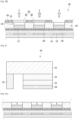
- a display 100 using a semiconductor light emitting element a display 100 using a passive matrix (PM) type of semiconductor light emitting element is exemplified.
- PM passive matrix
- AM active matrix
- the display 100 includes a first substrate 110, a first electrode 120, a conductive adhesive layer 130, a second electrode 140, and a plurality of semiconductor light emitting elements 150.
- the substrate 110 may be a flexible substrate.
- the substrate 110 may include glass or polyimide (PI) to implement a flexible display.
- PI polyimide
- any materials may be used as long as they have insulation and flexibility such as PEN (Polyethylene Naphthalate) and PET (Polyethylene Terephthalate).
- the substrate 110 may be made of any one of a transparent material or an opaque material.
- the substrate 110 may be a wiring board on which the first electrode 120 is disposed, so the first electrode 120 may be positioned on the substrate 110.
- an insulating layer 160 may be disposed over the substrate 110 on which the first electrode 120 is positioned, and an auxiliary electrode 170 may be positioned on the insulating layer 160.
- the state in which the insulating layer 160 is stacked on the substrate 110 may be one wiring board.
- the insulating layer 160 may be made of an insulating and flexible material, such as PI (Polyimide), PET, and PEN, integrally with the substrate 110, thereby forming one substrate.
- the auxiliary electrode 170 which is an electrode electrically connecting the semiconductor light emitting elements 150, is positioned on the insulating layer 160 and disposed to correspond to the first electrode 120.
- the auxiliary electrode 170 has a dot shape and can be electrically connected with the first electrode 120 by electrode holes 171 formed through the insulating layer 160.
- the electrode hole 171 may be formed by filing a via hole with a conductive material.
- the conductive adhesive layer 130 is formed on a surface of the insulating layer 160, but the present disclosure is not necessarily limited thereto.
- a structure, in which a layer performing a specific function is formed between the insulating layer 160 and the conductive adhesive layer 130 or the conductive adhesive layer 130 is disposed on the substrate 110 without the insulating layer 160 is possible.
- the conductive adhesive layer 130 can function as an insulating layer.
- the conductive adhesive layer 130 may be a layer having an adhesive property and conductivity, and to this end, a substance having conductivity and a substance having an adhesive property may be mixed in the conductive adhesive layer 130. Further, the conductive adhesive layer 130 has ductility, so it enables the flexible function of the display.
- the conductive adhesive layer 130 may be an anisotropy conductive film (ACF), an anisotropy conductive paste, and a solution containing conductive particles.
- ACF anisotropy conductive film
- the conductive adhesive layer 130 may be configured as a layer that allows for electrical connection in a Z direction passing through the thickness, but has electrical insulation in the horizontal X-Y direction. Accordingly, the conductive adhesive layer 130 may be referred to as a Z-axial conductive layer (however, hereafter, referred to as a 'conductive adhesive layer').
- the anisotropic conductive film is a film in which an anisotropic conductive medium is mixed in an insulating base member, and only a specific portion is given conductivity by the anisotropic conductive medium when heat and pressure are applied. It is assumed in the following description that heat and pressure are applied to the anisotropic conductive film, but other methods are also possible so that the anisotropic conductive film partially has conductivity. These methods, for example, may be a case of applying only any one of heat and pressure or a case of UV curing.
- the anisotropic conductive medium may be a conductive ball or a conductive particle.
- the anisotropic conductive film is a film in which conductive balls are mixed in an insulating base member, and only a specific portion is given conductivity by the conductive balls when heat and pressure are applied.
- the anisotropic conductive film may be in a state in which a plurality of particles coated with an insulating film made of a polymer material is contained in a core made of a conductive substance, and in this case, when heat and pressure are applied a portion, the insulating film is broken at the portion and the portion is given conductivity by the core.
- the shape of the core is deformed, so layers that are in contact with each other in the thickness direction of the film may be formed.
- heat and pressure are applied throughout the anisotropic conductive film and Z-axial electrical connection is partially formed by the height difference of an object that is bonded by the anisotropic conductive film.
- the anisotropic conductive film may be in a state in which a plurality of particles coated with a conductive substance is contained in an insulating core.
- the conductive substance at the portion is deformed (gets scored and sticks), so the portion is given conductivity in the thickness direction of the film.
- the conductive substance may pass through the insulating base member in the Z-axial direction to show conductivity in the thickness direction of the film. In this case, the conductive substance may have a pointed end.
- the anisotropic conductive film may be a fixed array ACF in which conductive balls are inserted in a surface of an insulating base member.
- the insulating base member is made of an adhesive substance, the conductive balls are concentrated at the bottom of the insulating base member, and when heat and pressure are applied to the base member, the base member is deformed with the conductive balls, thereby being given vertical conductivity.
- the anisotropic conductive film may be configured in a type in which conductive balls are randomly mixed in an insulating base member or a type in which a plurality of layers is provided and conductive balls are disposed in any one layer (double-ACF).
- the anisotropic conductive paste is formed by combining a paste and conductive balls, and may be a paste in which conductive balls are mixed in an insulating and adhesive base substance. Further, the solution containing conductive particles may be a solution containing conductive particles or nano particles.
- the second electrode 140 is spaced apart from the auxiliary electrode 170 and positioned on the insulating layer 160. That is, the conductive adhesive layer 130 is disposed on the insulating layer 160 on which the auxiliary electrode 170 and the second electrode 140 are positioned.
- the semiconductor light emitting element 150 is electrically connected with the first electrode 120 and the second electrode 140.
- the semiconductor light emitting element may be a flip-chip type light emitting element.
- the semiconductor light emitting element includes a p-type electrode 156, a p-type semiconductor layer 155 on which the p-type electrode 156 is formed, an active layer 154 formed on the p-type semiconductor layer 155, a n-type semiconductor layer 153 formed on the active layer 154, and a n-type electrode 152 horizontally spaced apart from the p-type electrode 156 on the n-type semiconductor layer 153.
- the p-type electrode 156 can be electrically connected with the auxiliary electrode 170 by the conductive adhesive layer 130
- the n-type electrode 152 can be electrically connected with the second electrode 140.
- the auxiliary electrode 170 is elongated in one direction and at least one auxiliary electrode can be electrically connected with a plurality of semiconductor light emitting elements 150.
- the p-type electrodes of semiconductor light emitting elements at left and right sides from an auxiliary electrode can be electrically connected with one auxiliary electrode.
- the semiconductor light emitting element 150 is pressed into the conductive adhesive layer 130 by heat and pressure, so only the portion between the p-type electrode 156 of the semiconductor light emitting element 150 and the auxiliary electrode 170 and the portion between the n-type electrode 152 of the semiconductor light emitting element 150 and the second electrode 140 have conductivity, and the other portions do not have conductivity because the semiconductor light emitting element is pressed inside.
- the conductive adhesive layer 130 not only couples, but also electrically connects the portion between the semiconductor light emitting element 150 and the auxiliary electrode 170 and the portion between the semiconductor light emitting element 150 and the second electrode 140.
- the plurality of semiconductor light emitting elements 150 constitutes a light emitting element array, and a fluorescent layer 180 is formed on the light emitting element array.
- the light emitting element array may include a plurality of semiconductor light emitting elements having different own luminance values.
- Each of the semiconductor light emitting element 150 constitutes a sub-pixel and is electrically connected to the first electrode 120.
- the first electrode 120 may be a plurality of pieces, the semiconductor light emitting elements, for example, may be arranged in several lines, and the semiconductor light emitting elements in each line may be electrically connected to any one of the plurality of first electrodes.
- the semiconductor light emitting elements are connected in a flip-chip type, it is possible to use grown semiconductor light emitting elements for a transparent dielectric substrate. Further, the semiconductor light emitting elements, for example, may be nitride semiconductor light emitting elements. Since the semiconductor light emitting element 150 has excellent luminance, it can constitute an individual sub-pixel even in a small size.
- a separation wall 190 may be formed between the semiconductor light emitting elements 150.
- the separation wall 190 can serve to separate individual sub-pixels and may be formed integrally with the conductive adhesive layer 130.
- the semiconductor light emitting elements 150 are inserted in the anisotropic conductive film, the base member of the anisotropic conductive film can form the separation wall.
- the separation wall 190 can have a reflective characteristic and the contrast can be increased even without a discrete black insulator.
- a reflective separation wall may be provided as the separation wall 190.
- the separation wall 190 may include a black or white insulator, depending on the object of the display.
- a separation wall of a white insulator is used, there can be an effect of increasing reflectivity, and when a separation wall of a black insulator, it is possible to have a reflective characteristic and increase contrast.
- the fluorescent layer 180 may be positioned on the outer side of the semiconductor light emitting element 150.
- the semiconductor light emitting element 150 is a blue semiconductor light emitting element that emits blue light (B), and the fluorescent layer 180 performs a function of converting the blue light (B) into a color of a sub-pixel.
- the fluorescent layer 180 may be a red fluorescent body 181 or a green fluorescent body 182 that constitutes an individual pixel.
- the red fluorescent body 181 that can convert blue light into red light (R) may be stacked on a blue semiconductor light emitting element at a position where a red sub-pixel is formed
- the green fluorescent body 182 that can convert blue light into green light (G) may be stacked on a blue semiconductor light emitting element at a position where a green sub-pixel is formed.
- only a blue semiconductor light emitting element may be independently used a portion forming a blue sub-pixel.
- red (R), green (G), and blue (B) sub-pixels can form one pixel.
- a fluorescent body having one color may be stacked along each line of the first electrode 120. Accordingly, in the first electrode 120, one line may be an electrode that controls one color. That is, red (R), green (G), and blue (B) may be sequentially disposed along the second electrode 140, whereby a sub-pixel can be implemented.
- red (R), green (G), and blue (B) sub-pixels may be implemented by combining the semiconductor light emitting element 150 and a quantum dot (QD) instead of a fluorescent body.
- QD quantum dot
- a black matrix 191 may be disposed between each of fluorescent bodies to improve contrast. That is, the black matrix 191 can improve the contrast of light and darkness.
- the semiconductor light emitting elements 150 each may be implemented as a high-power light emitting elements in which gallium nitride (GaN) is included as a main component and indium (In) and/or aluminum (Al) is added to emit various colors of light including blue.
- GaN gallium nitride
- In indium
- Al aluminum
- the semiconductor light emitting elements 150 may be red, green, and blue semiconductor light emitting elements to from sub-pixels respectively.
- red, green, and blue semiconductor light emitting elements R, G, B
- sub-pixels of red, green, and blue constitute one pixel by the red, green, and blue semiconductor light emitting elements, whereby a full-color display can be implemented.
- the semiconductor light emitting element may have white light emitting elements (W) each having a yellow fluorescent layer.
- W white light emitting elements
- a red fluorescent layer 181, a green fluorescent layer 182, and a blue fluorescent layer 183 may be disposed on the white light emitting element (W).
- a sub-pixel may be formed using a color filter in which red, green, and blue are repeated, on the white light emitting element (W).
- a structure in which a red fluorescent layer 181, a green fluorescent layer 182, and a blue fluorescent layer 183 are disposed on an ultraviolet light emitting element (UV) may be possible.
- a semiconductor light emitting element can be used in the entire region including not only the visual light, but also ultraviolet light (UV), and can be expanded in the type of a semiconductor light emitting element that can use ultraviolet light (UV) as an excitation source of an upper fluorescent body.
- the semiconductor light emitting element 150 is positioned on the conductive adhesive layer 130, thereby constituting a sub-pixel in the display. Since the semiconductor light emitting element 150 has excellent luminance, it can constitute an individual sub-pixel even in a small size.
- the individual semiconductor light emitting element 150 may have a size with one side of 80 ⁇ m or less and may be a rectangular or a square device. When it is a rectangle, the size may be 20 ⁇ 80 ⁇ m or less.
- a square semiconductor light emitting element 150 having one side length of 10 ⁇ m as a sub-pixel sufficient brightness for forming a display is shown. Accordingly, for example, in a case in which the size of a sub-pixel is a rectangular pixel having one side of 600 ⁇ m and the other one side of 300 ⁇ m, the distance of a semiconductor light emitting element is relatively sufficiently large. Accordingly, in this case, it is possible to implement a flexible display having high quality over HD quality.
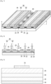
- the display using the semiconductor light emitting element described above can be manufactured by a new type of manufacturing method. Hereafter, this manufacturing method is described with reference to FIG. 6 .
- FIG. 6 shows cross-sectional views illustrating a method of manufacturing a display using a semiconductor light emitting element of the present disclosure not falling within the scope of the invention.
- the conductive adhesive layer 130 is formed on the insulating layer 160 on which the auxiliary electrode 170 and the second electrode 140 are positioned.
- the insulating layer 160 is stacked on the first substrate 110, thereby forming one substrate (wiring board). Further, the first electrode 120, the auxiliary electrode 170, and the second electrode 140 are disposed on the wiring board. In this case, the first electrode 120 and the second electrode 140 may be disposed perpendicular to each other. Further, in order to implement a flexible display, the first substrate 110 and the insulating layer 160 each may include glass or polyimide (PI).
- the conductive adhesive layer 130 may be implemented by an anisotropic conductive film, and to this end, an anisotropic conductive film may be applied to a substrate on which the insulating layer 160 is positioned.
- a second substrate 112 on which a plurality of semiconductor light emitting elements 150, which correspond to the positions of the auxiliary electrodes 170 and the second electrodes 140 and constitute individual pixels, is positioned is disposed such that the semiconductor light emitting elements 150 face the auxiliary electrodes 170 and the second electrodes 140.
- the second substrate 112 which is a growing substrate for growing the semiconductor light emitting elements 150, may be a spire substrate or a silicon substrate.
- the semiconductor light emitting elements have a gap and a size that can form a display when they are formed in a wafer unit, so they can be effectively used for a display.
- the wiring board and the second substrate 112 are thermally pressed.
- the wiring board and the second substrate 112 can be thermally pressed using an ACF press head.
- the wiring board and the second substrate 112 are bonded by the thermal pressing.
- Only the portions among the semiconductor light emitting element 150, the auxiliary electrode 170, and the second electrode 140 have conductivity by the characteristics of an anisotropic conductive film having conductivity by thermal pressing, so the electrodes and the semiconductor light emitting elements 150 can be electrically connected.
- the semiconductor light emitting elements 150 are inserted in the anisotropic conductive film, so separation walls may be formed between the semiconductor light emitting elements 150.
- the second substrate 112 is removed.
- LLO Laser Lift-off
- CLO Chemical Lift-off
- the semiconductor light emitting elements 150 are exposed to the outside by removing the second substrate 112. If necessary, it is possible to form a transparent insulating layer (not shown) by coating the top of the wiring board, to which the semiconductor light emitting elements 150 are coupled, with silicon oxide (SiOx), etc.
- the semiconductor light emitting element 150 may be a blue semiconductor light emitting element that emits blue light (B), and a red fluorescent body or a green fluorescent body for converting the blue light (B) into the light of a sub-pixel may form a layer on a surface of the blue semiconductor light emitting element.
- the manufacturing method or structure of the display using a semiconductor light emitting element described above can be modified in various ways.
- a vertical semiconductor light emitting element can also be applied to the display described above.
- a vertical structure is described with reference to FIGS. 5 and 6 .
- FIG. 7 is a perspective view showing another embodiment of a display using a semiconductor light emitting element of the present disclosure not falling within the scope of the invention
- FIG. 8 is a cross-sectional view taken along line D-D of FIG. 7
- FIG. 9 is a conceptual view showing a vertical semiconductor light emitting element of FIG. 8 .
- the display may be a display that uses passive matrix (PM) type of vertical semiconductor light emitting elements.
- PM passive matrix
- the display includes a substrate 210, a first electrode 220, a conductive adhesive layer 230, a second electrode 240, and a plurality of semiconductor light emitting elements 250.
- the substrate 210 which is a wiring board on which the first electrode 220 is disposed, may include polyimide (PI) to implement a flexible display. Further, any materials may be used as long as they have insulation and flexibility.
- PI polyimide
- the first electrode 220 is positioned on the substrate 210 and may be formed in a bar shape that is long in one direction.
- the first electrode 220 may be configured to function as a data electrode.
- the conductive adhesive layer 230 is formed on the substrate 210 on which the first electrode 220 is positioned.
- the conductive adhesive layer 230 may be an anisotropy conductive film (ACF), an anisotropy conductive paste, and a solution including conductive particles.
- ACF anisotropy conductive film
- anisotropy conductive paste an anisotropy conductive paste
- solution including conductive particles a solution including conductive particles.
- a case in which the conductive adhesive layer 230 is implemented by an anisotropic conductive film is exemplified.
- An isotropic conductive film is positioned in a state in which the first electrode 220 is positioned on the substrate 210 and then the semiconductor light emitting element 250 is connected by applying heat and pressure, the semiconductor light emitting element 250 is electrically connected with the first electrode 220.
- the semiconductor light emitting element 250 is disposed to be positioned on the first electrode 220.
- the electrical connection is generated because when heat and pressure are applied, the anisotropic conductive film partially has conductivity in the thickness direction. Accordingly, the anisotropic conductive film is divided into a portion having conductivity in the thickness direction and a portion not having conductivity in the thickness direction.
- the anisotropic conductive film contains an adhesive component
- the conductive adhesive layer 230 implements not only electrical connection, but also mechanical coupling between the semiconductor light emitting element 250 and the first electrode 220.
- the semiconductor light emitting element 250 is positioned on the conductive adhesive layer 230, whereby it configures an individual pixel in the display. Since the semiconductor light emitting element 250 has excellent luminance, it can constitute an individual sub-pixel even in a small size.
- the individual semiconductor light emitting element 250 may have a size with one side of 80 ⁇ m or less and may be a rectangular or a square device. When it is a rectangle, the size may be 20 ⁇ 80 ⁇ m or less.
- the semiconductor light emitting element 250 may be a vertical structure.
- a plurality of second electrodes 240 disposed across the length direction of the first electrode 220 and electrically connected with the vertical semiconductor light emitting elements 250 is positioned between the vertical semiconductor light emitting elements.
- the vertical semiconductor light emitting elements include a p-type electrode 256, a p-type semiconductor layer 255 formed on the p-type electrode 256, an active layer 254 formed on the p-type semiconductor layer 255, a n-type semiconductor layer 253 formed on the active layer 254, and a n-type electrode 252 formed on the n-type semiconductor layer 253.
- the p-type electrode 256 positioned at a lower portion can be electrically connected with the first electrode 220 by the conductive adhesive layer 230, and the n-type electrode 252 positioned at an upper portion can be electrically connected with the second electrode 240 to be described below.
- the semiconductor light emitting element 250 has a large advantage in that electrodes can be disposed up and down, so the chip size can be reduced.
- a fluorescent layer 280 may be formed on a surface of the semiconductor light emitting element 250.
- the semiconductor light emitting element 250 is a blue semiconductor light emitting element 251 that emits blue light (B), and the fluorescent layer 280 for converting the blue light (B) into a color of a sub-pixel can be provided.
- the fluorescent layer 280 may be a red fluorescent 281 and a green fluorescent body 282 constituting an individual pixel.
- the red fluorescent body 281 that can convert blue light into red light (R) may be stacked on a blue semiconductor light emitting element at a position where a red sub-pixel is formed
- the green fluorescent body 282 that can convert blue light into green light (G) may be stacked on a blue semiconductor light emitting element at a position where a green sub-pixel is formed.
- only a blue semiconductor light emitting element may be independently used a portion forming a blue sub-pixel. In this case, red (R), green (G), and blue (B) sub-pixels can form one pixel.
- the present disclosure is not necessarily limited thereto and other structures for implementing blue, green, and red, as described above, in a display to which flip-chip type light emitting elements are applied may be applied.
- the second electrodes 240 are disposed between the semiconductor light emitting elements 250 and electrically connected with the semiconductor light emitting elements.
- the semiconductor light emitting elements 250 may be disposed in a plurality of lines and the second electrodes 240 may be positioned between the lines of the semiconductor light emitting elements 250.
- the second electrodes 240 can be positioned between the semiconductor light emitting elements 250.
- the second electrode 240 may be formed as an electrode in a bar shape that is long in one direction and may be disposed perpendicular to the first electrode.
- the second electrode 240 and the semiconductor light emitting element 250 can be electrically connected by a connection electrode protruding from the second electrode 240.
- the connection electrode may be the n-type electrode of the semiconductor light emitting element 250.
- the n-type electrode is formed as an ohmic electrode for ohmic contact and the second electrode covers at least a portion of the ohmic electrode by printing or depositing. Accordingly, the second electrode 240 and the n-type electrode of the semiconductor light emitting element 250 can be electrically connected.
- the second electrode 240 may be positioned on the conductive adhesive layer 230.
- a transparent insulating layer (not shown) including silicon oxide (SiOx), etc may be formed on the substrate 210 on which the semiconductor light emitting elements 250 are formed.
- the second electrode 240 is positioned after the transparent insulating layer is formed, the second electrode 240 is positioned on the transparent insulating layer.
- the second electrodes 240 may be formed to be spaced apart from each other on the conductive adhesive layer 230 or the transparent insulating layer.
- the present disclosure has the advantage that there is no need for using a transparent electrode such as ITO by positioning the second electrode 240 between the semiconductor light emitting elements 250. Accordingly, it is possible to improve optical extraction efficiency by using a conductive substance, which is bonded well to a n-type semiconductor layer, as a horizontal electrode without being limited to selection of a transparent material.
- ITO Indium Tin Oxide
- a separation wall 290 may be positioned between the semiconductor light emitting elements 250. That is, the separation wall 290 may be disposed between the vertical semiconductor light emitting elements 250 to isolate the semiconductor light emitting elements 250 forming individual pixels. In this case, the separation wall 290 can serve to separate individual sub-pixels and may be formed integrally with the conductive adhesive layer 230. For example, the semiconductor light emitting elements 250 are inserted in the anisotropic conductive film, the base member of the anisotropic conductive film can form the separation wall.
- the separation wall 290 can have a reflective characteristic and the contrast can be increased even without a discrete black insulator.
- a reflective separation wall may be provided as the separation wall 190.
- the separation wall 290 may include a black or white insulator, depending on the object of the display.
- the separation wall 290 may be positioned between each of the semiconductor light emitting elements 250 and the second electrodes 240. Accordingly, there is an effect that it is possible to configure individual sub-pixels even in a small size using the semiconductor light emitting elements 250, it is possible to position the second electrode 240 between the semiconductor light emitting elements 250 because the distance of the semiconductor light emitting elements 250 is relatively larger, and it is possible to implement a flexible display having HD quality.
- a black matrix 291 may be disposed between fluorescent bodies to improve contrast. That is, the black matrix 291 can improve the contrast of light and darkness.
- the semiconductor light emitting element 250 is positioned on the conductive adhesive layer 230, whereby it configures an individual pixel in the display. Since the semiconductor light emitting element 250 has excellent luminance, it can constitute an individual sub-pixel even in a small size. Accordingly, a full-color display in which red (R), green (G), and blue (B) sub-pixels form one pixel by semiconductor light emitting elements can be implemented.
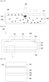
- FIG. 10 is a diagram showing an embodiment of a method of assembling a semiconductor light emitting element to a substrate.
- a semiconductor light emitting element 1000 can be put into a chamber 1300 filled with fluid 1200.
- the substrate 1100 can be disposed on the chamber 1300. Depending on embodiments, the substrate 1100 may be put into the chamber 1300.
- the coupling holes 1102 to which the semiconductor light emitting elements 1000 are coupled are formed in the substrate 1100 and the surface on which the coupling holes 1102 are formed can come in contact with the fluid 1200.
- the coupling holes 1102 may mean insulating through-holes formed through an insulating layer formed on a surface of the substrate 1100.
- an assembly apparatus 2000 can move along the substrate 1100.
- the assembly apparatus 2000 can move in contact with the substrate 1100 to maximize the region that a magnetic field reaches to the inside of the fluid 1200.
- the assembly apparatus 2000 may include a plurality of magnetic materials or a magnetic material having a size corresponding to the substrate 1100. In this case, the movement distance of the assembly apparatus 2000 may be limited within a predetermined range.
- the semiconductor light emitting element 1000 in the chamber 1300 can be moved toward the assembly apparatus 2000 by the magnetic field generated by the assembly apparatus 2000.
- the magnetic layer having a magnetic material e.g., nickel (Ni)
- Ni nickel
- the semiconductor light emitting element 1000 can be fitted and coupled into the coupling hole 1102 while moving toward the assembly apparatus 2000.
- a pattern or a shape for coupling in the correct direction may be formed in the coupling hole 1102 and/or the semiconductor light emitting element 1000.
- the self-assembling type that uses an electromagnetic field, it is possible to remarkably reduce the time that is taken to couple each of the semiconductor light emitting elements to the substrate, so it is possible to quickly and economically implement a large-area and high-pixel display.
- the magnetic layer of the semiconductor light emitting element 1000 is additionally inserted when a n-type electrode (or, a p-type electrode) is formed in the related art, so the magnetic layer may be disposed in a path through which light is extracted.
- the magnetic layer since the magnetic layer has low reflectance, the light extraction efficiency of the semiconductor light emitting element 1000 may be deteriorated.
- the smaller the size of the semiconductor light emitting element 1000 the more the light extraction efficiency is remarkably reduced.
- the structure and manufacturing method of the semiconductor light emitting element 1000 for solving this problem are described hereafter with reference to FIGS. 11 to 16 .
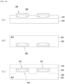
- FIG. 11 is a diagram showing an embodiment of the structure of a semiconductor light emitting element according to the invention related to the assembly method of FIG. 10.
- FIG. 12 is an enlarged view of the part A of FIG. 11 .
- FIG. 13 is a plan view showing the semiconductor light emitting element of FIG. 11 from above.
- the semiconductor light emitting element 1000 is a horizontal semiconductor light emitting element.
- the present disclosure is not limited only to a horizontal semiconductor light emitting element and may be similarly applied also to a vertical semiconductor light emitting element.
- an upward direction of the semiconductor light emitting element 1000 may mean the direction in which the p-type electrode 1020 is positioned and a downward direction may mean the direction in which the magnetic layer 1060 is positioned in the following figures.
- light that is emitted from the semiconductor light emitting element 1000 can be discharged outside through the upper portion of the semiconductor light emitting element 1000.
- the semiconductor light emitting element 1000 includes a p-type semiconductor layer 1010, a p-type electrode 1020 formed on the p-type semiconductor layer 1010, a n-type semiconductor layer 1030 formed under the p-type semiconductor layer 1010, and a n-type electrode 1040 formed in a partial region on the n-type semiconductor layer 1030.
- the partial region on the n-type semiconductor layer 1030 may be a region exposed by removing a portion of the p-type semiconductor layer 1010 through etching, etc.
- the p-type electrode 1020 may be implemented as a transparent electrode ((Indium Tin Oxide film; ITO) and the n-type electrode 1040 may be made of metal having high electrical conductivity for ohmic contact.
- ITO Indium Tin Oxide film
- the magnetic layer 1060 is formed under the n-type semiconductor layer 1030.
- the magnetic layer 1060 may include a magnetic material having magnetism such as nickel Ni.
- the magnetic layer 1060 is formed under the n-type semiconductor layer 1030. Accordingly, it is possible to prevent the problem of deterioration of light extraction efficiency due to failure to be discharged due to the magnetic layer 1060 when light is emitted through the upper portion of the semiconductor light emitting element 1000.
- the magnetic layer 1060 has low light reflection efficiency, some light traveling toward the magnetic layer 1060 of the light extracted from the semiconductor light emitting element 1000 may be absorbed by the magnetic layer 1060. In this case, a problem that the light extraction efficiency is not greatly improved may be generated.
- the semiconductor light emitting element 1000 further includes a reflective layer 1050 formed between the n-type semiconductor layer 1030 and the magnetic layer 1060.
- the reflective layer 1050 may be made of metal having high reflectance such as aluminum (Al) and silver (Ag).
- an assistant reflective layer 1070 may be further formed between the n-type electrode 1040 and the n-type semiconductor layer 1030.
- the assistant reflective layer 1070 may be made of metal (aluminum, etc.) having conductivity.
- light produced from the semiconductor light emitting element 1000 can be discharged outside through the upper portion of the p-type electrode 1020. That is, the pixel region of the semiconductor light emitting element 1000 may correspond to the p-type electrode 1020. In this case, the more the amount of the light discharged through the upper portion of the p-type electrode 1020, the more the light extraction efficiency of the semiconductor light emitting element 1000 can increase. Meanwhile, the semiconductor light emitting element 1000 may be formed in a circular shape when seen from above, but it is not necessary.
- the assistant reflective layer 1070 can reflect back the light traveling to the n-type electrode 1040 of the light reflective by the reflective layer 1050. Accordingly, much light can be discharged through the upper region of the p-type electrode 1020 that corresponds to the region through which light is emitted outside, so the light extraction efficiency can be further increased.
- the semiconductor light emitting element 1000 may further include a passivation layer 1080 surrounding the components 1010-1070 described above.
- the passivation layer 1080 may be formed to block the components 1010-1070 from the outside. Accordingly, it is possible to minimize the problem of inefficient assembly due to magnetization of the magnetic layer 1060 due to contact among the semiconductor light emitting elements put in the fluid 1200 or due to lumping of the semiconductor light emitting elements.
- n-type semiconductor layer 1030 the reflective layer 1050, and the magnetic layer 1060 are described in more detail hereafter with reference to FIG. 12 .
- the contact surfaces of the n-type semiconductor layer 1030 and the reflective layer 1050 are formed as non-planar surfaces.
- the contact surfaces may be formed as irregular non-planar surfaces. Accordingly, the light radiated to the reflective layer 1050 can be reflected in various directions, so the light uniformity of the semiconductor light emitting element 1000 can be improved.
- the semiconductor light emitting element 1000 includes a first adhesive member 1082 for increasing the adhesion between the n-type semiconductor layer 1030 and the reflective layer 1050 and a second adhesive member 1084 for increasing adhesion between the reflective layer 1050 and the magnetic layer 1060.
- the adhesive members 1082 and 1084 may be made of chromium (Cr) or Titanium (Ti).
- FIGS. 14 to 16 are diagrams for describing a method of manufacturing the semiconductor light emitting element according to the embodiment of FIG. 11 .
- a semiconductor growth process that sequentially grows the n-type semiconductor layer 1030 and the p-type semiconductor layer 1010 on a growth substrate 1400 may be performed.
- the growth substrate 1400 may be a sapphire substrate or a silicon substrate.
- a portion of the p-type semiconductor layer 1010 formed on the n-type semiconductor layer 1030 can be removed (etched, etc.) so that a portion of the n-type semiconductor layer 1030 is exposed upward.
- the semiconductor light emitting element 1000 is formed in a circular shape when seen from above, the other region except for a predetermined region can be removed with respect to the center portion of the p-type semiconductor layer 1010. Since a partial region of the p-type semiconductor layer 1010 is removed, a partial region of the n-type semiconductor layer 1030 can be exposed upward.
- the p-type electrode 1020 may be formed on the top surface of the p-type semiconductor layer 1010 and the n-type electrode 1040 may be formed on a portion of the top of the n-type semiconductor layer 1030.
- the p-type electrode 1020 may be implemented as a transparent electrode (ITO) to discharge light outside and the n-type electrode 1040 may be made of metal having high electric conductivity for ohmic contact.
- the assistant reflective layer 1070 is formed on a portion of the top surface of the n-type semiconductor layer 1030 and then the n-type electrode 1040 may be formed on the assistant reflective layer 1070.
- the passivation layer 1080 may be formed. In this case, since the bottom surface of the semiconductor light emitting element 1000 is in contact with the growth substrate 1400, the passivation layer 1080 may be formed on the top surface and the sides of the semiconductor light emitting element 1000.
- the growth substrate 1400 may be separated from the semiconductor light emitting element 1000 to form the reflective layer 1050 and the magnetic layer 1060 under the n-type semiconductor layer 1030.
- the semiconductor light emitting element 1000 may be fixed to another substrate (e.g., a temporary substrate 1410) after the growth substrate 1400 is separated.
- a temporary substrate 1410 e.g., a temporary substrate 1410
- an adhesive member 1420 that fixes the semiconductor light emitting element 1000 to the temporary substrate 1410 by being bonded to at least a portion of the top surface of the semiconductor light emitting element 1000 may have been applied to the temporary substrate 1410.
- the adhesive member 1420 may be made of PDMS (Polydimethylsiloxane), but is not limited thereto.
- the temporary substrate 1410 is made of a material having high heat resistance such as silicon, glass, sapphire, thereby being able to prevent deformation or damage, depending on the manufacturing process of the semiconductor light emitting element 1000 that is performed later.
- the growth substrate 1400 can be removed from the semiconductor light emitting element 1000 through an LLO (Laser Lift-Off) process.
- the semiconductor light emitting element 1000 can be fixed to the temporary substrate 1410 in a flipped type such that the n-type semiconductor layer 1030 faces up. Thereafter, a photoresist (PR) 1430 is applied to the flipped semiconductor light emitting element 1000 and the PR in the region corresponding to the n-type semiconductor layer 1030 can be removed through an exposure process.
- PR photoresist
- an etching process that etches a portion of the n-type semiconductor layer 1030 exposed upward may be performed.
- the etching process may correspond to a wet etching process that etches the n-type semiconductor layer 1030 using reactive ion etching (RIE), but is not limited thereto.
- RIE reactive ion etching
- An RIE apparatus can etch the n-type semiconductor layer 1030 using ions and radical existing due to etching gas (e.g., argon (Ar), chorine (Cl 2 ), or boron trichloride) produced in a plasma state.
- etching gas e.g., argon (Ar), chorine (Cl 2 ), or boron trichloride
- the etching process may be formed such that the etched surface of the n-type semiconductor layer 1030 becomes a non-planar surface (e.g., an irregular pattern).
- the vertical height of the etched surface may be maximally within 100nm, but is not limited thereto.
- the etched surface becomes a non-planar surface, light is reflected in various directions by the reflective layer 1050, so the light uniformity can be improved. Further, the coupling force between the n-type semiconductor layer 1030 and the reflective layer 1050 can be increased, as compared with the case in which the etched surface of a flat surface.
- a process of forming the reflective layer 1050 and the magnetic layer 1060 on the etched n-type semiconductor layer 1030 may be performed.
- the reflective layer 1050 and the magnetic layer 1060 may be deposited on the n-type semiconductor layer 1030 by electronic beam (E-beam) equipment.
- a process of depositing the first adhesive member 1082 on the n-type semiconductor layer 1030 may be performed first. Thereafter, the reflective layer 1050 is deposited on the first adhesive layer 1082, whereby the coupling force between the n-type semiconductor layer 1030 and the reflective layer 1050 can be improved.
- a process of depositing the second adhesive member 1084 on the reflective layer 1050 may be performed.
- a process of planarizing the top surface of the reflective layer 1050 may be performed first. The planarizing process can be performed by additionally depositing a reflective layer 1050, but is not necessarily limited thereto.
- the magnetic layer 1060 may be deposited on the second adhesive member1084. Since the planarizing process is performed, the magnetic layer 1060 can be formed with more uniform thickness.
- the reflective layer 1050 and the magnetic layer 1060 may be formed also on the photoresist 1430.
- the photoresist 1430, and the reflective layer and the magnetic layer formed on the photoresist 1430 can be removed from the temporary substrate 1410 and the semiconductor light emitting element 1000 through a lift-off process.
- the passivation layer 1080 for blocking the magnetic layer 1060 exposed to the outside from the outside may be additionally deposited. Accordingly, the components included in the semiconductor light emitting element 1000 can be blocked from the outside by the passivation layer 1080. Though not shown in the figures, regions of the passivation layer 108 that correspond to the p-type electrode 1020 and the n-type electrode 1040 may be removed (etched) for connection of power after being assembled to the substrate 1100 later.
- the temporary substrate 1410 and the adhesive member 1420 are removed from the semiconductor light emitting element 1000, and the semiconductor light emitting element 1000 can be put into the chamber 1300 filled with the fluid 1200.
- the semiconductor light emitting element 1000 is surrounded by the passivation layer 1080, so it is possible to prevent the fluid 1200 from permeating into the internal components 1010-1070.
- the substrate 1100 is disposed on the chamber 1300 (or put into the chamber 1300) and the assembly apparatus having a magnetic material is positioned over the substrate 1100, the semiconductor light emitting element 1000 in the fluid 1200 can be fitted and coupled in the coupling hole 1102 of the substrate 1100. Further, since an electric field is applied to the substrate 1100, it is possible to prevent the coupled semiconductor light emitting element 1000 from being separated by movement of the assembly apparatus 2000. Meanwhile, the coupling hole 1102 may be formed by removing (etching) a portion of the insulating layer 1104 formed on the substrate 1100.
Landscapes
- Led Device Packages (AREA)
- Devices For Indicating Variable Information By Combining Individual Elements (AREA)
- Led Devices (AREA)
- Electroluminescent Light Sources (AREA)
Claims (8)
- Lichtemittierendes Halbleiterelement (1000), das aufweist:eine n-Halbleiterschicht (1030);eine p-Halbleiterschicht (1010), die in einem ersten Bereich auf der n-Halbleiterschicht (1030) ausgebildet ist;eine p-Elektrode (1020), die auf der p-Halbleiterschicht (1010) ausgebildet ist;eine n-Elektrode (1040), die in einem zu dem ersten Bereich verschiedenen zweiten Bereich auf der n-Halbleiterschicht (1030) ausgebildet ist;eine magnetische Schicht (1060), die unter der n-Halbleiterschicht (1030) ausgebildet ist;eine reflektierende Schicht (1050), die zwischen der n-Halbleiterschicht (1030) und der magnetischen Schicht (1060) ausgebildet ist;dadurch gekennzeichnet, dassKontaktoberflächen der n-Halbleiterschicht (1030) und der reflektierenden Schicht (1050) als nicht planare Oberflächen ausgebildet sind; und dassdas lichtemittierende Halbleiterelement ferner aufweist:ein erstes Haftelement (1082), das zwischen der n-Halbleiterschicht (1030) und der reflektierenden Schicht (1050) ausgebildet ist; undein zweites Haftelement (1084), das zwischen der reflektierenden Schicht (1050) und der magnetischen Schicht (1060) ausgebildet ist.
- Lichtemittierendes Halbleiterelement nach Anspruch 1, wobei das erste Haftelement (1082) und das zweite Haftelement (1084) aus Chrom und/oder Titan hergestellt sind.
- Lichtemittierendes Halbleiterelement nach Anspruch 1, wobei die p-Elektrode (1020) als eine transparente Elektrode implementiert ist, und
die n-Elektrode (104) aus Metall hergestellt ist. - Lichtemittierendes Halbleiterelement nach Anspruch 3, das ferner eine reflektierende Hilfsschicht (1070) aufweist, die zwischen der n-Elektrode (1040) und der n-Halbleiterschicht (1030) ausgebildet ist.
- Lichtemittierendes Halbleiterelement nach Anspruch 1, das ferner eine Passivierungsschicht (1080) aufweist, welche die n-Halbleiterschicht (1030), die p-Halbleiterschicht (1010), die p-Elektrode (1020), die n-Elektrode (1040) und die magnetische Schicht (1060) umgibt.
- Lichtemittierendes Halbleiterelement nach Anspruch 1, wobei das erste Haftelement (1082) aus Chrom und/oder Titan hergestellt ist.
- Lichtemittierendes Halbleiterelement nach Anspruch 4, wobei die reflektierende Hilfsschicht (1070) auf einem Abschnitt einer oberen Oberfläche der n-Halbleiterschicht (1030) ausgebildet ist und die n-Elektrode (1040) auf der reflektierenden Hilfsschicht (1070) ausgebildet ist.
- Anzeigevorrichtung, welche das lichtemittierende Halbleiterelement nach einem de Ansprüche 1 bis 7 aufweist.
Applications Claiming Priority (2)
| Application Number | Priority Date | Filing Date | Title |
|---|---|---|---|
| KR1020190013019A KR20200095210A (ko) | 2019-01-31 | 2019-01-31 | 반도체 발광 소자, 이의 제조 방법, 및 이를 포함하는 디스플레이 장치 |
| PCT/KR2019/015820 WO2020159046A1 (en) | 2019-01-31 | 2019-11-19 | Semiconductor light emitting element, manufacturing method thereof, and display device including the same |
Publications (3)
| Publication Number | Publication Date |
|---|---|
| EP3918644A1 EP3918644A1 (de) | 2021-12-08 |
| EP3918644A4 EP3918644A4 (de) | 2022-10-26 |
| EP3918644B1 true EP3918644B1 (de) | 2024-02-07 |
Family
ID=71835759
Family Applications (1)
| Application Number | Title | Priority Date | Filing Date |
|---|---|---|---|
| EP19913545.0A Active EP3918644B1 (de) | 2019-01-31 | 2019-11-19 | Lichtemittierendes halbleiterelement |
Country Status (4)
| Country | Link |
|---|---|
| US (2) | US11233169B2 (de) |
| EP (1) | EP3918644B1 (de) |
| KR (1) | KR20200095210A (de) |
| WO (1) | WO2020159046A1 (de) |
Families Citing this family (8)
| Publication number | Priority date | Publication date | Assignee | Title |
|---|---|---|---|---|
| US11322645B1 (en) * | 2019-05-24 | 2022-05-03 | Innolux Corporation | Electronic device and manufacturing method thereof |
| US12027654B2 (en) * | 2020-09-11 | 2024-07-02 | Seoul Viosys Co., Ltd. | Unit pixel having light emitting device and displaying apparatus |
| TWI778490B (zh) * | 2021-01-08 | 2022-09-21 | 晶呈科技股份有限公司 | 具有順磁性發光元件之晶片結構及其製造方法 |
| JP7705035B2 (ja) * | 2021-09-21 | 2025-07-09 | 日亜化学工業株式会社 | 発光装置 |
| WO2023167350A1 (ko) * | 2022-03-04 | 2023-09-07 | 엘지전자 주식회사 | 반도체 발광 소자 및 디스플레이 장치 |
| CN119768911A (zh) * | 2022-07-21 | 2025-04-04 | Lg电子株式会社 | 包括半导体发光器件的显示装置 |
| WO2024122682A1 (ko) * | 2022-12-08 | 2024-06-13 | 엘지전자 주식회사 | 반도체 발광 소자 및 디스플레이 장치 |
| CN121126993B (zh) * | 2025-11-17 | 2026-04-21 | 上海显耀显示科技股份有限公司 | 发光二极管芯片 |
Family Cites Families (34)
| Publication number | Priority date | Publication date | Assignee | Title |
|---|---|---|---|---|
| US6784462B2 (en) * | 2001-12-13 | 2004-08-31 | Rensselaer Polytechnic Institute | Light-emitting diode with planar omni-directional reflector |
| TW517403B (en) * | 2002-01-10 | 2003-01-11 | Epitech Technology Corp | Nitride light emitting diode and manufacturing method for the same |
| US20050072968A1 (en) * | 2003-10-06 | 2005-04-07 | Tzong-Liang Tsai | Light-emitting device |
| US20050156183A1 (en) * | 2003-10-06 | 2005-07-21 | Tzong-Liang Tsai | Light-emitting device having reflecting layer formed under electrode |
| US7256483B2 (en) * | 2004-10-28 | 2007-08-14 | Philips Lumileds Lighting Company, Llc | Package-integrated thin film LED |
| US20070004066A1 (en) * | 2005-07-01 | 2007-01-04 | Dong-Sing Wuu | Method for manufacturing a light emitting device and a light emitting device manufactured therefrom |
| JP2007019318A (ja) * | 2005-07-08 | 2007-01-25 | Sumitomo Chemical Co Ltd | 半導体発光素子、半導体発光素子用基板の製造方法及び半導体発光素子の製造方法 |
| US20070214878A1 (en) | 2006-03-14 | 2007-09-20 | Core Laboratories Lp | Use of deuterium oxide-depleted water as a tracer in downhole and core analysis applications |
| US20070215878A1 (en) * | 2006-03-17 | 2007-09-20 | Dong-Sing Wuu | Light emitting device |
| DE102007002416A1 (de) * | 2006-04-13 | 2007-10-18 | Osram Opto Semiconductors Gmbh | Strahlungsemittierender Körper und Verfahren zur Herstellung eines strahlungsemittierenden Körpers |
| KR100974923B1 (ko) * | 2007-03-19 | 2010-08-10 | 서울옵토디바이스주식회사 | 발광 다이오드 |
| TWI350563B (en) * | 2007-07-10 | 2011-10-11 | Delta Electronics Inc | Manufacturing method of light emitting diode apparatus |
| TWI369009B (en) * | 2007-09-21 | 2012-07-21 | Nat Univ Chung Hsing | Light-emitting chip device with high thermal conductivity |
| WO2009039212A1 (en) * | 2007-09-21 | 2009-03-26 | Bridgelux, Inc. | Light-emitting diode chip with high extraction and method for manufacturing the same |
| TWI370560B (en) * | 2007-12-14 | 2012-08-11 | Delta Electronics Inc | Light-emitting diode device and manufacturing method thereof |
| US8502259B2 (en) * | 2008-01-11 | 2013-08-06 | Industrial Technology Research Institute | Light emitting device |
| US8536614B2 (en) * | 2008-01-11 | 2013-09-17 | Industrial Technology Research Institute | Nitride semiconductor light emitting device with magnetic film |
| US7906786B2 (en) * | 2008-01-11 | 2011-03-15 | Industrial Technology Research Institute | Light emitting device |
| US7928463B2 (en) * | 2008-01-11 | 2011-04-19 | Industrial Technology Research Institute | Light emitting device |
| DE102008005115A1 (de) | 2008-01-14 | 2009-07-16 | Siemens Aktiengesellschaft | Schaltgerät, insbesondere Leistungsschaltgerät, mit zwei in Reihe, geschalteten Schaltkontaktpaaren zur Unterbrechung einer Strombahn |
| KR101047718B1 (ko) * | 2008-11-26 | 2011-07-08 | 엘지이노텍 주식회사 | 발광 소자 |
| KR20100092116A (ko) * | 2009-02-12 | 2010-08-20 | 광주과학기술원 | 자기 구조체를 구비하는 발광다이오드 및 자기 구조체를 구비하는 발광다이오드 패키지 |
| JP2010225852A (ja) * | 2009-03-24 | 2010-10-07 | Panasonic Corp | 半導体素子及びその製造方法 |
| US9437785B2 (en) * | 2009-08-10 | 2016-09-06 | Cree, Inc. | Light emitting diodes including integrated backside reflector and die attach |
| JP5659519B2 (ja) * | 2009-11-19 | 2015-01-28 | 豊田合成株式会社 | 発光装置、発光装置の製造方法、発光装置の実装方法及び光源装置 |
| KR20110110957A (ko) * | 2010-04-02 | 2011-10-10 | (주)엘이디팩 | Led 패키지 |
| TWI447975B (zh) * | 2012-01-05 | 2014-08-01 | 矽品精密工業股份有限公司 | 發光二極體晶片之結構、發光二極體封裝基板之結構、發光二極體封裝結構及其製法 |
| WO2013141421A1 (ko) * | 2012-03-22 | 2013-09-26 | 주식회사 씨엘포토닉스 | 수평형 파워 led 소자 및 그 제조방법 |
| KR101618771B1 (ko) * | 2012-05-10 | 2016-05-09 | 광주과학기술원 | 자성층을 구비한 플립칩형 발광소자 및 그 제조방법 |
| KR101983774B1 (ko) * | 2012-09-20 | 2019-05-29 | 엘지이노텍 주식회사 | 발광 소자 |
| KR102249645B1 (ko) * | 2014-11-05 | 2021-05-10 | 엘지이노텍 주식회사 | 발광소자, 이를 포함하는 발광소자 패키지, 및 이를 포함하는 조명시스템 |
| KR101873729B1 (ko) | 2016-11-11 | 2018-07-04 | 서울대학교산학협력단 | 표면 보호층이 형성된 리튬 음극 제조방법, 이에 따라 제조된 리튬 음극 및 이를 적용한 리튬 이차전지 |
| US10217895B2 (en) * | 2017-06-22 | 2019-02-26 | Epistar Corporation | Method of forming a light-emitting device |
| KR102419593B1 (ko) * | 2017-10-23 | 2022-07-12 | 삼성전자주식회사 | 발광 다이오드 및 그의 제조 방법 |
-
2019
- 2019-01-31 KR KR1020190013019A patent/KR20200095210A/ko not_active Ceased
- 2019-11-19 EP EP19913545.0A patent/EP3918644B1/de active Active
- 2019-11-19 WO PCT/KR2019/015820 patent/WO2020159046A1/en not_active Ceased
- 2019-11-21 US US16/691,113 patent/US11233169B2/en active Active
-
2021
- 2021-12-14 US US17/550,743 patent/US11978821B2/en active Active
Also Published As
| Publication number | Publication date |
|---|---|
| US20200251608A1 (en) | 2020-08-06 |
| US11233169B2 (en) | 2022-01-25 |
| US20220102579A1 (en) | 2022-03-31 |
| US11978821B2 (en) | 2024-05-07 |
| EP3918644A4 (de) | 2022-10-26 |
| KR20200095210A (ko) | 2020-08-10 |
| WO2020159046A1 (en) | 2020-08-06 |
| EP3918644A1 (de) | 2021-12-08 |
Similar Documents
| Publication | Publication Date | Title |
|---|---|---|
| EP3918644B1 (de) | Lichtemittierendes halbleiterelement | |
| US12113161B2 (en) | Display device using micro LED and method for manufacturing same | |
| EP4050657B1 (de) | Anzeigevorrichtung mit mikro-led und herstellungsverfahren dafür | |
| US12557441B2 (en) | Display device using micro-LEDs and method for manufacturing same | |
| KR102413330B1 (ko) | 반도체 발광소자를 이용한 디스플레이 장치 | |
| US12362335B2 (en) | Display device using micro LED and method of manufacturing same | |
| EP4020568B1 (de) | Anzeigevorrichtung mit mikro-led und herstellungsverfahren dafür | |
| US12322733B2 (en) | Display device using semiconductor light-emitting elements, and method for manufacturing same | |
| US20220367774A1 (en) | Display device using micro led, and manufacturing method therefor | |
| KR101968527B1 (ko) | 반도체 발광 소자를 이용한 디스플레이 장치 및 이의 제조방법 | |
| KR20190097946A (ko) | 반도체 발광소자를 이용한 디스플레이 장치의 제조방법 | |
| US11502055B2 (en) | Assembly apparatus for assembling semiconductor light emitting diode to display panel | |
| KR102557154B1 (ko) | 반도체 발광 소자를 이용한 디스플레이 장치 | |
| KR20190083566A (ko) | 반도체 발광소자를 이용한 디스플레이 장치 | |
| KR102766068B1 (ko) | 반도체 발광소자 및 반도체 발광소자를 이용한 디스플레이 장치 | |
| US12300767B2 (en) | Display apparatus using micro LED and method for manufacturing same | |
| KR102357645B1 (ko) | 반도체 발광소자를 이용한 디스플레이 장치 | |
| KR102110871B1 (ko) | 반도체 발광소자를 이용한 디스플레이 장치 | |
| KR20200026774A (ko) | 반도체 발광 소자를 이용한 디스플레이 장치 및 이의 제조방법 | |
| US12426422B2 (en) | Display device having support module on side surface of substrate | |
| KR102639607B1 (ko) | 반도체 발광소자를 이용한 디스플레이 장치의 제조방법 | |
| KR102876067B1 (ko) | 반도체 발광 소자를 이용한 디스플레이 장치 및 그 제조 방법 | |
| EP3871262B1 (de) | Anzeigevorrichtung mit lichtemittierendem halbleiterbauelement und verfahren zur herstellung davon | |
| CN121730001A (zh) | 转移基板组装体及利用其的显示装置的制造方法 | |
| KR20260056188A (ko) | 전사 기판 조립체 및 이를 이용한 디스플레이 장치의 제조 방법 |
Legal Events
| Date | Code | Title | Description |
|---|---|---|---|
| STAA | Information on the status of an ep patent application or granted ep patent |
Free format text: STATUS: THE INTERNATIONAL PUBLICATION HAS BEEN MADE |
|
| PUAI | Public reference made under article 153(3) epc to a published international application that has entered the european phase |
Free format text: ORIGINAL CODE: 0009012 |
|
| STAA | Information on the status of an ep patent application or granted ep patent |
Free format text: STATUS: REQUEST FOR EXAMINATION WAS MADE |
|
| 17P | Request for examination filed |
Effective date: 20210806 |
|
| AK | Designated contracting states |
Kind code of ref document: A1 Designated state(s): AL AT BE BG CH CY CZ DE DK EE ES FI FR GB GR HR HU IE IS IT LI LT LU LV MC MK MT NL NO PL PT RO RS SE SI SK SM TR |
|
| DAV | Request for validation of the european patent (deleted) | ||
| DAX | Request for extension of the european patent (deleted) | ||
| A4 | Supplementary search report drawn up and despatched |
Effective date: 20220926 |
|
| RIC1 | Information provided on ipc code assigned before grant |
Ipc: H01L 33/46 20100101ALN20220920BHEP Ipc: H01L 25/075 20060101ALN20220920BHEP Ipc: H01L 23/00 20060101ALI20220920BHEP Ipc: H01L 33/44 20100101ALI20220920BHEP Ipc: H01L 33/00 20100101AFI20220920BHEP |
|
| RIC1 | Information provided on ipc code assigned before grant |
Ipc: H01L 33/46 20100101ALN20230710BHEP Ipc: H01L 25/075 20060101ALN20230710BHEP Ipc: H01L 21/683 20060101ALI20230710BHEP Ipc: H01L 23/00 20060101ALI20230710BHEP Ipc: H01L 33/44 20100101ALI20230710BHEP Ipc: H01L 33/00 20100101AFI20230710BHEP |
|
| RIC1 | Information provided on ipc code assigned before grant |
Ipc: H01L 33/46 20100101ALN20230718BHEP Ipc: H01L 25/075 20060101ALN20230718BHEP Ipc: H01L 21/683 20060101ALI20230718BHEP Ipc: H01L 23/00 20060101ALI20230718BHEP Ipc: H01L 33/44 20100101ALI20230718BHEP Ipc: H01L 33/00 20100101AFI20230718BHEP |
|
| GRAP | Despatch of communication of intention to grant a patent |
Free format text: ORIGINAL CODE: EPIDOSNIGR1 |
|
| STAA | Information on the status of an ep patent application or granted ep patent |
Free format text: STATUS: GRANT OF PATENT IS INTENDED |
|
| RIC1 | Information provided on ipc code assigned before grant |
Ipc: H01L 33/46 20100101ALN20230828BHEP Ipc: H01L 25/075 20060101ALN20230828BHEP Ipc: H01L 21/683 20060101ALI20230828BHEP Ipc: H01L 23/00 20060101ALI20230828BHEP Ipc: H01L 33/44 20100101ALI20230828BHEP Ipc: H01L 33/00 20100101AFI20230828BHEP |
|
| INTG | Intention to grant announced |
Effective date: 20230912 |
|
| GRAS | Grant fee paid |
Free format text: ORIGINAL CODE: EPIDOSNIGR3 |
|
| GRAA | (expected) grant |
Free format text: ORIGINAL CODE: 0009210 |
|
| STAA | Information on the status of an ep patent application or granted ep patent |
Free format text: STATUS: THE PATENT HAS BEEN GRANTED |
|
| AK | Designated contracting states |
Kind code of ref document: B1 Designated state(s): AL AT BE BG CH CY CZ DE DK EE ES FI FR GB GR HR HU IE IS IT LI LT LU LV MC MK MT NL NO PL PT RO RS SE SI SK SM TR |
|
| REG | Reference to a national code |
Ref country code: GB Ref legal event code: FG4D |
|
| REG | Reference to a national code |
Ref country code: CH Ref legal event code: EP |
|
| REG | Reference to a national code |
Ref country code: IE Ref legal event code: FG4D |
|
| REG | Reference to a national code |
Ref country code: DE Ref legal event code: R096 Ref document number: 602019046345 Country of ref document: DE |
|
| REG | Reference to a national code |
Ref country code: LT Ref legal event code: MG9D |
|
| REG | Reference to a national code |
Ref country code: NL Ref legal event code: MP Effective date: 20240207 |
|
| PG25 | Lapsed in a contracting state [announced via postgrant information from national office to epo] |
Ref country code: IS Free format text: LAPSE BECAUSE OF FAILURE TO SUBMIT A TRANSLATION OF THE DESCRIPTION OR TO PAY THE FEE WITHIN THE PRESCRIBED TIME-LIMIT Effective date: 20240607 |
|
| PG25 | Lapsed in a contracting state [announced via postgrant information from national office to epo] |
Ref country code: LT Free format text: LAPSE BECAUSE OF FAILURE TO SUBMIT A TRANSLATION OF THE DESCRIPTION OR TO PAY THE FEE WITHIN THE PRESCRIBED TIME-LIMIT Effective date: 20240207 |
|
| PG25 | Lapsed in a contracting state [announced via postgrant information from national office to epo] |
Ref country code: GR Free format text: LAPSE BECAUSE OF FAILURE TO SUBMIT A TRANSLATION OF THE DESCRIPTION OR TO PAY THE FEE WITHIN THE PRESCRIBED TIME-LIMIT Effective date: 20240508 |
|
| REG | Reference to a national code |
Ref country code: AT Ref legal event code: MK05 Ref document number: 1655932 Country of ref document: AT Kind code of ref document: T Effective date: 20240207 |
|
| PG25 | Lapsed in a contracting state [announced via postgrant information from national office to epo] |
Ref country code: NL Free format text: LAPSE BECAUSE OF FAILURE TO SUBMIT A TRANSLATION OF THE DESCRIPTION OR TO PAY THE FEE WITHIN THE PRESCRIBED TIME-LIMIT Effective date: 20240207 Ref country code: HR Free format text: LAPSE BECAUSE OF FAILURE TO SUBMIT A TRANSLATION OF THE DESCRIPTION OR TO PAY THE FEE WITHIN THE PRESCRIBED TIME-LIMIT Effective date: 20240207 Ref country code: RS Free format text: LAPSE BECAUSE OF FAILURE TO SUBMIT A TRANSLATION OF THE DESCRIPTION OR TO PAY THE FEE WITHIN THE PRESCRIBED TIME-LIMIT Effective date: 20240507 |
|
| PG25 | Lapsed in a contracting state [announced via postgrant information from national office to epo] |
Ref country code: ES Free format text: LAPSE BECAUSE OF FAILURE TO SUBMIT A TRANSLATION OF THE DESCRIPTION OR TO PAY THE FEE WITHIN THE PRESCRIBED TIME-LIMIT Effective date: 20240207 |
|
| PG25 | Lapsed in a contracting state [announced via postgrant information from national office to epo] |
Ref country code: AT Free format text: LAPSE BECAUSE OF FAILURE TO SUBMIT A TRANSLATION OF THE DESCRIPTION OR TO PAY THE FEE WITHIN THE PRESCRIBED TIME-LIMIT Effective date: 20240207 |
|
| PG25 | Lapsed in a contracting state [announced via postgrant information from national office to epo] |
Ref country code: RS Free format text: LAPSE BECAUSE OF FAILURE TO SUBMIT A TRANSLATION OF THE DESCRIPTION OR TO PAY THE FEE WITHIN THE PRESCRIBED TIME-LIMIT Effective date: 20240507 Ref country code: NO Free format text: LAPSE BECAUSE OF FAILURE TO SUBMIT A TRANSLATION OF THE DESCRIPTION OR TO PAY THE FEE WITHIN THE PRESCRIBED TIME-LIMIT Effective date: 20240507 Ref country code: NL Free format text: LAPSE BECAUSE OF FAILURE TO SUBMIT A TRANSLATION OF THE DESCRIPTION OR TO PAY THE FEE WITHIN THE PRESCRIBED TIME-LIMIT Effective date: 20240207 Ref country code: LT Free format text: LAPSE BECAUSE OF FAILURE TO SUBMIT A TRANSLATION OF THE DESCRIPTION OR TO PAY THE FEE WITHIN THE PRESCRIBED TIME-LIMIT Effective date: 20240207 Ref country code: IS Free format text: LAPSE BECAUSE OF FAILURE TO SUBMIT A TRANSLATION OF THE DESCRIPTION OR TO PAY THE FEE WITHIN THE PRESCRIBED TIME-LIMIT Effective date: 20240607 Ref country code: HR Free format text: LAPSE BECAUSE OF FAILURE TO SUBMIT A TRANSLATION OF THE DESCRIPTION OR TO PAY THE FEE WITHIN THE PRESCRIBED TIME-LIMIT Effective date: 20240207 Ref country code: GR Free format text: LAPSE BECAUSE OF FAILURE TO SUBMIT A TRANSLATION OF THE DESCRIPTION OR TO PAY THE FEE WITHIN THE PRESCRIBED TIME-LIMIT Effective date: 20240508 Ref country code: FI Free format text: LAPSE BECAUSE OF FAILURE TO SUBMIT A TRANSLATION OF THE DESCRIPTION OR TO PAY THE FEE WITHIN THE PRESCRIBED TIME-LIMIT Effective date: 20240207 Ref country code: ES Free format text: LAPSE BECAUSE OF FAILURE TO SUBMIT A TRANSLATION OF THE DESCRIPTION OR TO PAY THE FEE WITHIN THE PRESCRIBED TIME-LIMIT Effective date: 20240207 Ref country code: BG Free format text: LAPSE BECAUSE OF FAILURE TO SUBMIT A TRANSLATION OF THE DESCRIPTION OR TO PAY THE FEE WITHIN THE PRESCRIBED TIME-LIMIT Effective date: 20240207 Ref country code: AT Free format text: LAPSE BECAUSE OF FAILURE TO SUBMIT A TRANSLATION OF THE DESCRIPTION OR TO PAY THE FEE WITHIN THE PRESCRIBED TIME-LIMIT Effective date: 20240207 |
|
| PG25 | Lapsed in a contracting state [announced via postgrant information from national office to epo] |
Ref country code: PT Free format text: LAPSE BECAUSE OF FAILURE TO SUBMIT A TRANSLATION OF THE DESCRIPTION OR TO PAY THE FEE WITHIN THE PRESCRIBED TIME-LIMIT Effective date: 20240607 Ref country code: PL Free format text: LAPSE BECAUSE OF FAILURE TO SUBMIT A TRANSLATION OF THE DESCRIPTION OR TO PAY THE FEE WITHIN THE PRESCRIBED TIME-LIMIT Effective date: 20240207 |
|
| PG25 | Lapsed in a contracting state [announced via postgrant information from national office to epo] |
Ref country code: SE Free format text: LAPSE BECAUSE OF FAILURE TO SUBMIT A TRANSLATION OF THE DESCRIPTION OR TO PAY THE FEE WITHIN THE PRESCRIBED TIME-LIMIT Effective date: 20240207 Ref country code: PT Free format text: LAPSE BECAUSE OF FAILURE TO SUBMIT A TRANSLATION OF THE DESCRIPTION OR TO PAY THE FEE WITHIN THE PRESCRIBED TIME-LIMIT Effective date: 20240607 Ref country code: PL Free format text: LAPSE BECAUSE OF FAILURE TO SUBMIT A TRANSLATION OF THE DESCRIPTION OR TO PAY THE FEE WITHIN THE PRESCRIBED TIME-LIMIT Effective date: 20240207 Ref country code: LV Free format text: LAPSE BECAUSE OF FAILURE TO SUBMIT A TRANSLATION OF THE DESCRIPTION OR TO PAY THE FEE WITHIN THE PRESCRIBED TIME-LIMIT Effective date: 20240207 |
|
| PG25 | Lapsed in a contracting state [announced via postgrant information from national office to epo] |
Ref country code: DK Free format text: LAPSE BECAUSE OF FAILURE TO SUBMIT A TRANSLATION OF THE DESCRIPTION OR TO PAY THE FEE WITHIN THE PRESCRIBED TIME-LIMIT Effective date: 20240207 |
|
| PG25 | Lapsed in a contracting state [announced via postgrant information from national office to epo] |
Ref country code: SM Free format text: LAPSE BECAUSE OF FAILURE TO SUBMIT A TRANSLATION OF THE DESCRIPTION OR TO PAY THE FEE WITHIN THE PRESCRIBED TIME-LIMIT Effective date: 20240207 |
|
| PG25 | Lapsed in a contracting state [announced via postgrant information from national office to epo] |
Ref country code: CZ Free format text: LAPSE BECAUSE OF FAILURE TO SUBMIT A TRANSLATION OF THE DESCRIPTION OR TO PAY THE FEE WITHIN THE PRESCRIBED TIME-LIMIT Effective date: 20240207 Ref country code: EE Free format text: LAPSE BECAUSE OF FAILURE TO SUBMIT A TRANSLATION OF THE DESCRIPTION OR TO PAY THE FEE WITHIN THE PRESCRIBED TIME-LIMIT Effective date: 20240207 |
|
| PG25 | Lapsed in a contracting state [announced via postgrant information from national office to epo] |
Ref country code: SK Free format text: LAPSE BECAUSE OF FAILURE TO SUBMIT A TRANSLATION OF THE DESCRIPTION OR TO PAY THE FEE WITHIN THE PRESCRIBED TIME-LIMIT Effective date: 20240207 |
|
| PG25 | Lapsed in a contracting state [announced via postgrant information from national office to epo] |
Ref country code: SM Free format text: LAPSE BECAUSE OF FAILURE TO SUBMIT A TRANSLATION OF THE DESCRIPTION OR TO PAY THE FEE WITHIN THE PRESCRIBED TIME-LIMIT Effective date: 20240207 Ref country code: SK Free format text: LAPSE BECAUSE OF FAILURE TO SUBMIT A TRANSLATION OF THE DESCRIPTION OR TO PAY THE FEE WITHIN THE PRESCRIBED TIME-LIMIT Effective date: 20240207 Ref country code: RO Free format text: LAPSE BECAUSE OF FAILURE TO SUBMIT A TRANSLATION OF THE DESCRIPTION OR TO PAY THE FEE WITHIN THE PRESCRIBED TIME-LIMIT Effective date: 20240207 Ref country code: EE Free format text: LAPSE BECAUSE OF FAILURE TO SUBMIT A TRANSLATION OF THE DESCRIPTION OR TO PAY THE FEE WITHIN THE PRESCRIBED TIME-LIMIT Effective date: 20240207 Ref country code: DK Free format text: LAPSE BECAUSE OF FAILURE TO SUBMIT A TRANSLATION OF THE DESCRIPTION OR TO PAY THE FEE WITHIN THE PRESCRIBED TIME-LIMIT Effective date: 20240207 Ref country code: CZ Free format text: LAPSE BECAUSE OF FAILURE TO SUBMIT A TRANSLATION OF THE DESCRIPTION OR TO PAY THE FEE WITHIN THE PRESCRIBED TIME-LIMIT Effective date: 20240207 |
|
| REG | Reference to a national code |
Ref country code: DE Ref legal event code: R097 Ref document number: 602019046345 Country of ref document: DE |
|
| REG | Reference to a national code |
Ref country code: DE Ref legal event code: R079 Ref document number: 602019046345 Country of ref document: DE Free format text: PREVIOUS MAIN CLASS: H01L0033000000 Ipc: H10H0020000000 |
|
| PG25 | Lapsed in a contracting state [announced via postgrant information from national office to epo] |
Ref country code: IT Free format text: LAPSE BECAUSE OF FAILURE TO SUBMIT A TRANSLATION OF THE DESCRIPTION OR TO PAY THE FEE WITHIN THE PRESCRIBED TIME-LIMIT Effective date: 20240207 |
|
| PLBE | No opposition filed within time limit |
Free format text: ORIGINAL CODE: 0009261 |
|
| STAA | Information on the status of an ep patent application or granted ep patent |
Free format text: STATUS: NO OPPOSITION FILED WITHIN TIME LIMIT |
|
| PG25 | Lapsed in a contracting state [announced via postgrant information from national office to epo] |
Ref country code: IT Free format text: LAPSE BECAUSE OF FAILURE TO SUBMIT A TRANSLATION OF THE DESCRIPTION OR TO PAY THE FEE WITHIN THE PRESCRIBED TIME-LIMIT Effective date: 20240207 |
|
| 26N | No opposition filed |
Effective date: 20241108 |
|
| PG25 | Lapsed in a contracting state [announced via postgrant information from national office to epo] |
Ref country code: SI Free format text: LAPSE BECAUSE OF FAILURE TO SUBMIT A TRANSLATION OF THE DESCRIPTION OR TO PAY THE FEE WITHIN THE PRESCRIBED TIME-LIMIT Effective date: 20240207 |
|
| REG | Reference to a national code |
Ref country code: CH Ref legal event code: PL |
|
| PG25 | Lapsed in a contracting state [announced via postgrant information from national office to epo] |
Ref country code: MC Free format text: LAPSE BECAUSE OF FAILURE TO SUBMIT A TRANSLATION OF THE DESCRIPTION OR TO PAY THE FEE WITHIN THE PRESCRIBED TIME-LIMIT Effective date: 20240207 |
|
| PG25 | Lapsed in a contracting state [announced via postgrant information from national office to epo] |
Ref country code: LU Free format text: LAPSE BECAUSE OF NON-PAYMENT OF DUE FEES Effective date: 20241119 |
|
| REG | Reference to a national code |
Ref country code: CH Ref legal event code: PL |
|
| GBPC | Gb: european patent ceased through non-payment of renewal fee |
Effective date: 20241119 |
|
| PG25 | Lapsed in a contracting state [announced via postgrant information from national office to epo] |
Ref country code: CH Free format text: LAPSE BECAUSE OF NON-PAYMENT OF DUE FEES Effective date: 20241130 |
|
| REG | Reference to a national code |
Ref country code: BE Ref legal event code: MM Effective date: 20241130 |
|
| PG25 | Lapsed in a contracting state [announced via postgrant information from national office to epo] |
Ref country code: GB Free format text: LAPSE BECAUSE OF NON-PAYMENT OF DUE FEES Effective date: 20241119 Ref country code: BE Free format text: LAPSE BECAUSE OF NON-PAYMENT OF DUE FEES Effective date: 20241130 |
|
| PG25 | Lapsed in a contracting state [announced via postgrant information from national office to epo] |
Ref country code: IE Free format text: LAPSE BECAUSE OF NON-PAYMENT OF DUE FEES Effective date: 20241119 |
|
| PGFP | Annual fee paid to national office [announced via postgrant information from national office to epo] |
Ref country code: DE Payment date: 20251002 Year of fee payment: 7 |
|
| PGFP | Annual fee paid to national office [announced via postgrant information from national office to epo] |
Ref country code: FR Payment date: 20251001 Year of fee payment: 7 |
|
| PG25 | Lapsed in a contracting state [announced via postgrant information from national office to epo] |
Ref country code: HU Free format text: LAPSE BECAUSE OF FAILURE TO SUBMIT A TRANSLATION OF THE DESCRIPTION OR TO PAY THE FEE WITHIN THE PRESCRIBED TIME-LIMIT; INVALID AB INITIO Effective date: 20191119 |
|
| PG25 | Lapsed in a contracting state [announced via postgrant information from national office to epo] |
Ref country code: CY Free format text: LAPSE BECAUSE OF FAILURE TO SUBMIT A TRANSLATION OF THE DESCRIPTION OR TO PAY THE FEE WITHIN THE PRESCRIBED TIME-LIMIT; INVALID AB INITIO Effective date: 20191119 |