US7928463B2 - Light emitting device - Google Patents
Light emitting device Download PDFInfo
- Publication number
- US7928463B2 US7928463B2 US12/436,798 US43679809A US7928463B2 US 7928463 B2 US7928463 B2 US 7928463B2 US 43679809 A US43679809 A US 43679809A US 7928463 B2 US7928463 B2 US 7928463B2
- Authority
- US
- United States
- Prior art keywords
- light emitting
- emitting device
- layer
- light
- type layer
- Prior art date
- Legal status (The legal status is an assumption and is not a legal conclusion. Google has not performed a legal analysis and makes no representation as to the accuracy of the status listed.)
- Active, expires
Links
- 230000005291 magnetic effect Effects 0.000 claims abstract description 116
- 239000000696 magnetic material Substances 0.000 claims abstract description 24
- 239000000463 material Substances 0.000 claims description 41
- 239000004065 semiconductor Substances 0.000 claims description 14
- 238000002347 injection Methods 0.000 claims description 10
- 239000007924 injection Substances 0.000 claims description 10
- 229910052751 metal Inorganic materials 0.000 claims description 9
- 239000002184 metal Substances 0.000 claims description 9
- AMGQUBHHOARCQH-UHFFFAOYSA-N indium;oxotin Chemical compound [In].[Sn]=O AMGQUBHHOARCQH-UHFFFAOYSA-N 0.000 claims description 5
- 229910010272 inorganic material Inorganic materials 0.000 claims description 4
- 239000011147 inorganic material Substances 0.000 claims description 4
- 150000004767 nitrides Chemical class 0.000 claims description 3
- 239000011368 organic material Substances 0.000 claims description 3
- 229910001218 Gallium arsenide Inorganic materials 0.000 claims description 2
- XLOMVQKBTHCTTD-UHFFFAOYSA-N Zinc monoxide Chemical compound [Zn]=O XLOMVQKBTHCTTD-UHFFFAOYSA-N 0.000 claims description 2
- 239000002210 silicon-based material Substances 0.000 claims description 2
- 238000009826 distribution Methods 0.000 description 18
- 238000010586 diagram Methods 0.000 description 12
- 239000000758 substrate Substances 0.000 description 12
- 238000005424 photoluminescence Methods 0.000 description 10
- 230000008901 benefit Effects 0.000 description 9
- 239000010931 gold Substances 0.000 description 9
- PXHVJJICTQNCMI-UHFFFAOYSA-N nickel Substances [Ni] PXHVJJICTQNCMI-UHFFFAOYSA-N 0.000 description 9
- 230000000694 effects Effects 0.000 description 8
- 238000005086 pumping Methods 0.000 description 6
- 239000004020 conductor Substances 0.000 description 5
- 239000010949 copper Substances 0.000 description 5
- 230000006872 improvement Effects 0.000 description 5
- 239000004593 Epoxy Substances 0.000 description 4
- 238000000576 coating method Methods 0.000 description 4
- 229910052802 copper Inorganic materials 0.000 description 4
- 230000002708 enhancing effect Effects 0.000 description 4
- BASFCYQUMIYNBI-UHFFFAOYSA-N platinum Substances [Pt] BASFCYQUMIYNBI-UHFFFAOYSA-N 0.000 description 4
- 239000010409 thin film Substances 0.000 description 4
- 230000005355 Hall effect Effects 0.000 description 3
- -1 MnAs Inorganic materials 0.000 description 3
- PCHJSUWPFVWCPO-UHFFFAOYSA-N gold Chemical compound [Au] PCHJSUWPFVWCPO-UHFFFAOYSA-N 0.000 description 3
- 229910052742 iron Inorganic materials 0.000 description 3
- 229910052748 manganese Inorganic materials 0.000 description 3
- 238000012986 modification Methods 0.000 description 3
- 230000004048 modification Effects 0.000 description 3
- 229910052759 nickel Inorganic materials 0.000 description 3
- 238000004806 packaging method and process Methods 0.000 description 3
- 229910052697 platinum Inorganic materials 0.000 description 3
- 238000009827 uniform distribution Methods 0.000 description 3
- 229910001020 Au alloy Inorganic materials 0.000 description 2
- 229910000990 Ni alloy Inorganic materials 0.000 description 2
- WCUXLLCKKVVCTQ-UHFFFAOYSA-M Potassium chloride Chemical compound [Cl-].[K+] WCUXLLCKKVVCTQ-UHFFFAOYSA-M 0.000 description 2
- XUIMIQQOPSSXEZ-UHFFFAOYSA-N Silicon Chemical compound [Si] XUIMIQQOPSSXEZ-UHFFFAOYSA-N 0.000 description 2
- BQCADISMDOOEFD-UHFFFAOYSA-N Silver Chemical compound [Ag] BQCADISMDOOEFD-UHFFFAOYSA-N 0.000 description 2
- 229910052804 chromium Inorganic materials 0.000 description 2
- 239000011651 chromium Substances 0.000 description 2
- 238000013461 design Methods 0.000 description 2
- QDOXWKRWXJOMAK-UHFFFAOYSA-N dichromium trioxide Chemical compound O=[Cr]O[Cr]=O QDOXWKRWXJOMAK-UHFFFAOYSA-N 0.000 description 2
- PQXKHYXIUOZZFA-UHFFFAOYSA-M lithium fluoride Chemical compound [Li+].[F-] PQXKHYXIUOZZFA-UHFFFAOYSA-M 0.000 description 2
- 238000000034 method Methods 0.000 description 2
- IOLCXVTUBQKXJR-UHFFFAOYSA-M potassium bromide Chemical compound [K+].[Br-] IOLCXVTUBQKXJR-UHFFFAOYSA-M 0.000 description 2
- 230000008569 process Effects 0.000 description 2
- FGDZQCVHDSGLHJ-UHFFFAOYSA-M rubidium chloride Chemical compound [Cl-].[Rb+] FGDZQCVHDSGLHJ-UHFFFAOYSA-M 0.000 description 2
- 229910052710 silicon Inorganic materials 0.000 description 2
- 239000010703 silicon Substances 0.000 description 2
- 229910052709 silver Inorganic materials 0.000 description 2
- 239000004332 silver Substances 0.000 description 2
- 238000012360 testing method Methods 0.000 description 2
- 229910052720 vanadium Inorganic materials 0.000 description 2
- RYGMFSIKBFXOCR-UHFFFAOYSA-N Copper Chemical compound [Cu] RYGMFSIKBFXOCR-UHFFFAOYSA-N 0.000 description 1
- 229910019963 CrSb Inorganic materials 0.000 description 1
- 229910016629 MnBi Inorganic materials 0.000 description 1
- 229910017231 MnTe Inorganic materials 0.000 description 1
- 229910052779 Neodymium Inorganic materials 0.000 description 1
- 229910052772 Samarium Inorganic materials 0.000 description 1
- 229910021607 Silver chloride Inorganic materials 0.000 description 1
- 229910045601 alloy Inorganic materials 0.000 description 1
- 239000000956 alloy Substances 0.000 description 1
- 230000004075 alteration Effects 0.000 description 1
- 229910052782 aluminium Inorganic materials 0.000 description 1
- XAGFODPZIPBFFR-UHFFFAOYSA-N aluminium Chemical compound [Al] XAGFODPZIPBFFR-UHFFFAOYSA-N 0.000 description 1
- 229910052787 antimony Inorganic materials 0.000 description 1
- 150000001649 bromium compounds Chemical class 0.000 description 1
- 229910010293 ceramic material Inorganic materials 0.000 description 1
- 238000006243 chemical reaction Methods 0.000 description 1
- 150000003841 chloride salts Chemical class 0.000 description 1
- 239000011248 coating agent Substances 0.000 description 1
- MPTQRFCYZCXJFQ-UHFFFAOYSA-L copper(II) chloride dihydrate Chemical compound O.O.[Cl-].[Cl-].[Cu+2] MPTQRFCYZCXJFQ-UHFFFAOYSA-L 0.000 description 1
- 239000000412 dendrimer Substances 0.000 description 1
- 229920000736 dendritic polymer Polymers 0.000 description 1
- 238000011161 development Methods 0.000 description 1
- 238000005516 engineering process Methods 0.000 description 1
- 230000005294 ferromagnetic effect Effects 0.000 description 1
- 239000003302 ferromagnetic material Substances 0.000 description 1
- 239000010408 film Substances 0.000 description 1
- 150000002222 fluorine compounds Chemical class 0.000 description 1
- 239000011521 glass Substances 0.000 description 1
- 229910052737 gold Inorganic materials 0.000 description 1
- 239000011133 lead Substances 0.000 description 1
- 230000005415 magnetization Effects 0.000 description 1
- 239000011572 manganese Substances 0.000 description 1
- 238000004519 manufacturing process Methods 0.000 description 1
- 230000007246 mechanism Effects 0.000 description 1
- 230000005693 optoelectronics Effects 0.000 description 1
- 230000009467 reduction Effects 0.000 description 1
- 229910052701 rubidium Inorganic materials 0.000 description 1
- 229910052707 ruthenium Inorganic materials 0.000 description 1
- HKZLPVFGJNLROG-UHFFFAOYSA-M silver monochloride Chemical compound [Cl-].[Ag+] HKZLPVFGJNLROG-UHFFFAOYSA-M 0.000 description 1
- XOLBLPGZBRYERU-UHFFFAOYSA-N tin dioxide Chemical compound O=[Sn]=O XOLBLPGZBRYERU-UHFFFAOYSA-N 0.000 description 1
- 229910001887 tin oxide Inorganic materials 0.000 description 1
- 230000009466 transformation Effects 0.000 description 1
- 238000002834 transmittance Methods 0.000 description 1
Images


Classifications
-
- H—ELECTRICITY
- H10—SEMICONDUCTOR DEVICES; ELECTRIC SOLID-STATE DEVICES NOT OTHERWISE PROVIDED FOR
- H10H—INORGANIC LIGHT-EMITTING SEMICONDUCTOR DEVICES HAVING POTENTIAL BARRIERS
- H10H20/00—Individual inorganic light-emitting semiconductor devices having potential barriers, e.g. light-emitting diodes [LED]
-
- H—ELECTRICITY
- H10—SEMICONDUCTOR DEVICES; ELECTRIC SOLID-STATE DEVICES NOT OTHERWISE PROVIDED FOR
- H10K—ORGANIC ELECTRIC SOLID-STATE DEVICES
- H10K50/00—Organic light-emitting devices
- H10K50/80—Constructional details
-
- H—ELECTRICITY
- H10—SEMICONDUCTOR DEVICES; ELECTRIC SOLID-STATE DEVICES NOT OTHERWISE PROVIDED FOR
- H10H—INORGANIC LIGHT-EMITTING SEMICONDUCTOR DEVICES HAVING POTENTIAL BARRIERS
- H10H20/00—Individual inorganic light-emitting semiconductor devices having potential barriers, e.g. light-emitting diodes [LED]
- H10H20/80—Constructional details
- H10H20/85—Packages
-
- H—ELECTRICITY
- H10—SEMICONDUCTOR DEVICES; ELECTRIC SOLID-STATE DEVICES NOT OTHERWISE PROVIDED FOR
- H10K—ORGANIC ELECTRIC SOLID-STATE DEVICES
- H10K50/00—Organic light-emitting devices
- H10K50/80—Constructional details
- H10K50/84—Passivation; Containers; Encapsulations
-
- H—ELECTRICITY
- H10—SEMICONDUCTOR DEVICES; ELECTRIC SOLID-STATE DEVICES NOT OTHERWISE PROVIDED FOR
- H10K—ORGANIC ELECTRIC SOLID-STATE DEVICES
- H10K59/00—Integrated devices, or assemblies of multiple devices, comprising at least one organic light-emitting element covered by group H10K50/00
- H10K59/80—Constructional details
- H10K59/87—Passivation; Containers; Encapsulations
Definitions
- the prior application Ser. No. 12/146,418 and Ser. No. 12/146,422 are continuation applications of and claim the priority benefit of the said non-provisional application Ser. No. 12/117,747.
- the prior application Ser. No. 12/351,815 is a continuation-in-part application of and claims priority benefits of the said non-provisional application Ser. No. 12/117,747, the said non-provisional application Ser. No. 12/146,418, the said non-provisional application Ser. No. 12/146,422, and U.S. non-provisional application Ser. No. 12/168,073, filed on Jul. 4, 2008 and also claims the priority benefit of the said provisional application Ser.
- the disclosure generally relates to a light emitting device, and in particular, to a light emitting device with a magnetic field.
- Light emitting device such as a light emitting diode (LED) can emit light due to the driving of electron current through the active layer of the light emitting diode.
- LED light emitting diode
- the non-transparent top electrode in conventional design, is usually positioned at the center region of the light emitting area. In this manner, the current density under the top electrode is larger than the other region and can emit more light.
- the emitted light under the top electrode is blocked since the top electrode is not transparent to the light.
- the top electrode of the conventional LED blocks the emitted light at the central region with the highest intensity, resulting in reduction of the output light.
- the disclosure is directed to a light emitting device with magnetic field, so as to at least improve light emitting efficiency.
- the light emitting device of the disclosure which includes a light-emitting structure and a magnetic material.
- the light-emitting structure has an exciting binding energy of a bandgap.
- the magnetic material is coupled with the light-emitting structure to produce a magnetic field in the light-emitting structure.
- the exciting binding energy may be higher than about 25.8 meV at room temperature.
- the light emitting device of the disclosure includes a light-emitting structure and a magnetic material.
- the light-emitting structure includes a P-type layer, a light emitting layer, an N-type layer, and a transparent conductive layer.
- the N-type layer has an electrical resistivity ⁇ n , a thickness t n and a carrier mobility ⁇ n
- the transparent conductive layer has an electrical resistivity ⁇ t , a thickness t t and a carrier mobility ⁇ t .
- a current flows through the N-type layer within a depth t nI in a cross-section of the N-type layer, and the depth t nI is smaller than or equal to the thickness t n .
- the magnetic material is coupled with the light-emitting structure to produce a magnetic field B in the light-emitting structure. While the magnetic field B provided by the magnetic material is applied to the light emitting device, a magnetoresistance of the transparent conductive layer
- ⁇ t t t ⁇ ( 1 + ⁇ t 2 ⁇ B 2 ) is substantially equal to a magnetoresistance of the N-type layer
- the magnetic material is integrated into the structure of the light emitting device.
- the magnetic field is separately self-supplied in a single light emitting device.
- the single light emitting device can also be easily packaged into a chip. Therefore, the magnetic field can be applied to the light emitting device in the manners as described above, so as to enhance the light emitting efficiency and increase the luminance of the light emitting device.
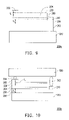
- FIG. 1 depicts, in a cross-sectional view, a light emitting device according to an embodiment of the disclosure.
- FIGS. 2-5 are schematic cross-sectional diagrams schematically illustrating a light emitting device according to an embodiment of the disclosure, respectively.
- FIGS. 6A-6B are cross-sectional diagrams schematically illustrating a light emitting device according to an embodiment of the disclosure, respectively.
- FIG. 7A schematically illustrates distribution curves of wavelength versus PL intensity under various pumping power of laser according to a light emitting device without applying the magnetic field.
- FIG. 7B schematically illustrates distribution curves of wavelength versus PL intensity under various pumping power of laser according to a light emitting device with applying the magnetic field.
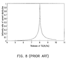
- FIG. 8 schematically illustrates a distribution curve of thickness of TCL versus uniformity ratio of current distribution according to a conventional light emitting device without the application of the magnetic field.
- FIGS. 9-11 are schematic cross-sectional diagrams schematically illustrating a light emitting device according to an embodiment of the disclosure, respectively.
- FIG. 12A schematically illustrates distribution curves of injected current versus forward voltage according to a light emitting device with and without the application of the magnetic field, respectively.
- FIG. 12B schematically illustrates distribution curves of injected current versus emitting power according to a light emitting device with and without the application of the magnetic field, respectively.
- the disclosure involves the consideration of the Hall effect and implements the Hall effect into light emitting devices.
- FIG. 1 depicts, in a cross-sectional view, a structure of a light emitting device with the magnetic field according to an embodiment of the disclosure.
- a light emitting diode LED
- the light emitting diode includes, for example, a bottom electrode 100 , a light-emitting structure 102 , a top electrode 104 .
- the light-emitting stacked layer 102 includes, for example, a first doped layer 102 a , such as P-doped layer, an active layer 102 b for emitting light based on combination of electrons and holes, and a second doped layer 102 c , such as N-doped layer.
- the top electrode 104 can be, for example, not position at the center of the light emitting area 108 .
- the current flows from the bottom electrode 100 to the top electrode 104 .
- an external magnetic field in a direction such as an indication to go in the paper as designated by notion 106
- the Lorenz force is produced to shift and spread the current, as shown in FIG. 1 .
- Alterations or modifications of the conductive types of the electrodes and the direction of the magnetic field are allowed according to the actual design, while the concept remains the same.
- the current are transversely shifted and can still flow from the bottom electrode to the top electrode, which is at the side region of the light emitting area 108 .
- the driving current can more effectively cause the active layer 102 b to emit light.
- the two electrodes 100 and 104 are at opposite sides of the light-emitting stacked layer 102 , and then the magnetic is applied parallel to the light emitting area 180 , in which the driving current is shifted inside light-emitting stacked layer 102 .
- the electrode is arranged at the same side of the light-emitting stacked layer, a large horizontal-component current is produced, and the direction of magnetic field can be accordingly changed.
- the magnetic field applied to the light emitting device can also improve the conversion efficiency for producing light in the light emitting device.
- the basic mechanism is that exertion of the magnetic field can increase exciting binding energy of a bandgap in material of the active region, resulting in enhancing the probability of carrier combination.
- the exciting binding energy between the conductive band and the valence band can be closer to the valence band with the aid of the magnetic field, and thereby the internal quantum efficiency (IQE) in the material of the light emitting device can be enhanced effectively.
- the improvement is more significant for the material having the exciting binding energy higher than thermal voltage at room temperature, e.g. about 25.8 meV.
- the light-emitting structure of the light emitting device includes a semiconductor material with the desirable exciting binding energy.
- the light-emitting structure of the light emitting device may include an inorganic material with the exciting binding energy higher than 25.8 meV.
- the inorganic material can be a nitride-based material, such as GaN.
- Other inorganic materials with the exciting binding energy higher than 25.8 meV e.g. Si, CdS, BaO, KI, KCl, KBr, RbCl, LiF and AgCl, can also be employed to the light-emitting structure.
- the light-emitting structure of the light emitting device may include an organic material with the exciting binding energy higher than 25.8 meV, such as phosphorescence material, fluorescent material, etc.
- the phosphorescence material can be red, green, blue or dendrimer
- the fluorescent material can be red, green, blue, yellow or white, for example.
- the exciting binding energy in the semiconductor material would increase as the magnitude of the applied magnetic field rises.
- the disclosure proposes that the magnetic field applied to the light emitting device can extra increase the exciting binding energy, the IQE and the carrier combination, such that the light emitting efficiency is remarkably improved.
- the light emitting device With the external magnetic field applied to the light emitting device, not only the homogeneity of the carrier density in the semiconductor is altered, but also the light emitting efficiency is enhanced. Accordingly, the light emitting device has higher luminance efficiency for optoelectronic transformation even though the amount of injected current remains unchanged.
- the intensity of the external magnetic field applied to the light emitting device may be larger than 0.01 gauss (G), for example.
- the magnetic field can be provided by a magnet, a magnetic thin film, an electromagnet, or any other kind of magnetic material, and the number thereof is not limited herein.
- the magnetic material may be coupled to the light emitting device itself in the form of a magnetic film or a magnetic bulk, depending upon the thickness thereof.
- the direction of the magnetic field may be properly arranged, such as vertical arrangement, horizontal arrangement or any direction relative to the light emitting device.
- the magnetic material may be a ferromagnetic material, such as Rb, Ru, Nd, Fe, Pg, Co, Ni, Mn, Cr, Cu, Cr 2 , Pt, Sm, Sb, Pt, or an alloy of the foregoing materials in combination.
- a ferromagnetic material such as Rb, Ru, Nd, Fe, Pg, Co, Ni, Mn, Cr, Cu, Cr 2 , Pt, Sm, Sb, Pt, or an alloy of the foregoing materials in combination.
- the magnetic material may also be a ceramic material, such as oxides of Mn, Fe, Co, Cu and V, Cr 2 O 3 , CrS, MnS, MnSe, MnTe, fluorides of Mn, Fe, Co and Ni, chlorides of V, Cr, Fe, Co, Ni and Cu, bromides of Cu, CrSb, MnAs, MnBi, ⁇ -Mn, MnCl 2 .4H 2 O, MnBr 2 .4H 2 O, CuCl 2 .2H 2 O, Co(NH 4 )x(SO 4 )xCl 2 .6H 2 O, FeCo 3 , and FeCo 3 .2MgCO 3 .
- the light emitting device can be an inorganic LED or an organic LED (OLED), either in a vertical type, a horizontal type, a thin film type or a flip chip type.
- the light emitting device can be combined with magnetic material through various manners such as epoxy, metal bonding, wafer bonding, epitaxial embedding and coating.
- Embodiments of the light emitting device with the magnetic material adopting foregoing structures are described as follows, respectively. It is noted that the following embodiments in which the first conductivity type is P-type and the second conductivity type is N-type is provided for illustration purposes, and should not be construed as limiting the scope of the disclosure.
- FIG. 2 is a schematic cross-sectional diagram illustrating a light emitting device according to an embodiment of the disclosure.
- the light emitting device 200 is a horizontal type LED, which includes a light-emitting structure coupled with a magnetic material.
- the light-emitting structure is disposed on a magnetic submount 220 through an epoxy, a metal bonding, a wafer bonding, epitaxial embedding, or a coating process.
- the magnetic submount 220 is, for example, a ferromagnetic layer with a magnetization in a desired direction.
- the light-emitting structure includes a first electrode 202 , a first doped layer 204 , an active layer 206 , a second doped layer 208 , a second electrode 210 , and a substrate 212 .
- the substrate 212 is mounted on the magnetic submount 220 .
- the first doped layer 204 such as a P-type doped layer
- the first electrode 202 is disposed on the first doped layer 204 and electrically coupled to the first doped layer 204 .
- the second electrode 210 is disposed at the same side of the first electrode 202 and electrically coupled to the second doped layer 208 . Accordingly, a horizontal type LED structure is formed.
- the active layer 206 is disposed between the first doped layer 204 and the second doped layer 208 , and capable of generating light when a current flows through it.
- the magnetic field generated by the magnetic submount 220 is exerted on the light-emitting structure, such that the exciting binding energy of the semiconductor material in the light-emitting structure is increased to enhance an overall emitting efficiency of the light emitting device 200 .
- FIG. 3 is a schematic cross-sectional diagram illustrating a light emitting device according to an embodiment of the disclosure.
- the identical elements shown in FIGS. 2 and 3 are designated with the same reference numbers, and detailed descriptions of the same or like elements are omitted hereinafter.
- the structural components of the light emitting device 300 are roughly similar to that of the light emitting device 200 shown in FIG. 2 , while the difference lies in the deployment of the magnetic material.
- a packaging structure such as a flip chip package, can be employed to couple the magnetic material with the light-emitting structure.
- the first electrode 202 and the second electrode 210 of the light-emitting structure can be mounted onto a magnetic submount 320 .
- the light-emitting structure may be packaged onto the magnetic submount 320 through the bonding structures 302 and 304 .
- the bonding structures 302 and 304 are, for example, bounding bumps.
- the light-emitting structure may be directly bonding onto the magnetic submount 320 without any bonding structures. That is to say, the first electrode 202 and the second electrode 210 can be directly mounted on the surface of the magnetic submount 320 .
- the magnetic submount 320 can produce the magnet field into the light emitting device 300 , and the exciting binding energy of the semiconductor material in the light-emitting structure is thus increased to enhance the emitting efficiency of the light emitting device 300 .
- FIG. 4 is a schematic cross-sectional diagram illustrating a light emitting device according to an embodiment of the disclosure.
- FIG. 4 is a schematic cross-sectional diagram illustrating a light emitting device according to one embodiment of the disclosure.
- the light emitting device 400 in this embodiment is a vertical type LED, which includes a light-emitting structure and a magnetic submount 420 .
- the light-emitting structure is disposed on the magnetic submount 420 through an epoxy, a metal bonding, a wafer bonding, epitaxial embedding, or a coating process.
- the light-emitting structure includes, from top to bottom, a second electrode 402 , a second doped layer 404 , an active layer 406 , a first doped layer 408 and a first electrode 410 .
- the magnetic submount 420 serves as a substrate for the light-emitting structure.
- the second doped layer 404 , the active layer 406 , and the first doped layer 408 form a light-emitting stacked layer, which is deployed on the magnetic submount 420 .
- the second electrode 402 is disposed on the second doped layer 404 and electrically coupled to the second doped layer 404 .
- the first electrode 410 is disposed between the first doped layer 408 and the magnetic submount 420 , and electrically coupled to the first doped layer 408 . Accordingly, a vertical type LED structure is formed.
- the active layer 406 is disposed between the second doped layer 404 and the first doped layer 408 , and capable of generating light when a current flows through it.
- the magnetic field induced by the magnetic submount 420 is exerted on light-emitting structure, such that the exciting binding energy of the semiconductor material in the light-emitting structure is increased to enhance an overall emitting efficiency of the light emitting device 400 .
- FIG. 5 is a cross-sectional diagram schematically illustrating a light emitting device according to an embodiment of the disclosure.
- the light emitting device 500 includes a light-emitting structure coupled with an embedded magnetic material.
- the magnetic layer 520 can be formed between a substrate 512 and the light-emitting structure 514 based on the technology of epitaxial laterally overgrown (ELOG).
- the magnetic layer 520 may be formed on the substrate 512 and then patterned into the intended pattern, such as strip or block. Thereafter, a lower semiconductor layer of the light-emitting structure 514 can be grown by ELOG process.
- the magnetic layer 520 embedded in the semiconductor material provide the magnetic field to the light emitting device 500 for enhancing the exciting binding energy thereof. Accordingly, the luminous efficiency of the light emitting device 500 is efficaciously advanced by the application of the magnetic field.
- FIGS. 6A-6B are cross-sectional diagrams schematically illustrating a light emitting device according to an embodiment of the disclosure, respectively.
- the identical elements shown in FIGS. 6A and 6B are designated with the same reference numbers, and detailed descriptions of the same or like elements are omitted hereinafter.
- the light emitting device 600 which includes a light-emitting structure coupled with a magnetic layer 620 .
- the light-emitting structure is disposed on a magnetic layer 620 through an epoxy, a metal bonding, a wafer bonding, epitaxial embedding, or a coating process.
- the light-emitting structure is, for example, a stacked structure of an organic electroluminescent device (OLED), which includes a substrate 602 , an anode layer 604 , a hole transporting layer (HTL) 606 , an electroluminescent layer 608 , an electron transporting layer (ETL) 610 and a cathode layer 612 .
- OLED organic electroluminescent device
- the substrate 602 is disposed on the magnetic layer 620
- the anode layer 604 is disposed on the surface of the substrate 602 .
- the hole transporting layer (HTL) 606 , the electroluminescent layer 608 and the electron transporting layer (ETL) 610 are, for example, stacked between the anode layer 604 and the cathode layer 612 , wherein the electroluminescent layer 608 is disposed between the hole transporting layer (HTL) 606 and the electron transporting layer (ETL) 610 .
- the substrate 602 can be a transparent substrate, e.g. a glass substrate.
- the anode layer 604 is typically composed of metal or transparent conductive material, such as indium tin oxide (ITO), silicon, tin oxide, gold, silver, platinum or copper.
- the anode layer 604 may be a transparent conductive layer including indium tin oxide (ITO) or silicon.
- the hole transporting layer (HTL) 606 , the electroluminescent layer 608 and the electron transporting layer (ETL) 610 can be composed of organic material, respectively.
- the cathode layer 612 may include metal or a transparent conductive material, such as aluminum, silver or indium tin oxide (ITO).
- ITO indium tin oxide
- the light emitting device 600 may further include a hole injection layer (HIL) 614 and an electron injection layer (EIL) 616 in the stacked structure.
- the hole injection layer (HIL) 614 is deployed between the hole transporting layer (HTL) 606 and the anode layer 604 .
- the electron injection layer (EIL) 616 is deployed between the cathode layer 612 and the electron transporting layer (ETL) 610 .
- the organic light-emitting structure can also be implemented by containing at least one of the foregoing layers between the anode layer 604 and the cathode layer 612 , and is not construed as limiting the scope of the disclosure.
- an offset voltage is applied between the anode layer 604 and the cathode layer 612 , electrons are injected into the electron transporting layer (ETL) 610 from the cathode layer 612 and are transmitted to the electroluminescent layer 608 , while holes are injected into the hole transporting layer (HTL) 606 from the anode layer 604 . Further, the injected holes are transmitted to the electroluminescent layer 608 , where the electrons and the holes are recombined to generate excitons and produce luminous effect.
- the magnetic field generated by the magnetic layer 620 is exerted on the light-emitting structure, such that the exciting binding energy of the material in the light-emitting structure is increased to enhance an overall emitting efficiency of the light emitting device 600 .
- the organic light emitting device can have another configuration. As shown in FIG. 6B , the structural components of the light emitting device 600 a are roughly similar to that of the light emitting device 600 shown in FIG. 6A , while the difference lies in the deployment of the magnetic layer 620 a .
- a packaging structure e.g. a flip chip package, can be employed to couple the magnetic layer 620 a with the light-emitting structure.
- the stacked light-emitting structure may be packaged with the magnetic layer 620 a by mounting the cathode layer 612 to the magnetic layer 620 a , so as to form the flip chip structure.
- the magnetic field generated by the magnetic layer 620 a can increase the exciting binding energy of the material in the light-emitting structure, thereby enhancing an overall emitting efficiency of the light emitting device 600 a.
- FIG. 7A schematically illustrates distribution curves of wavelength versus PL intensity under various pumping power of laser according to a light emitting device without applying the magnetic field.
- FIG. 7B schematically illustrates distribution curves of wavelength versus PL intensity under various pumping power of laser according to a light emitting device with applying the magnetic field.
- a GaN chip is utilized as a sample, of which the exciting binding energy is higher than 25.8 meV.
- Different intensity of the laser is then pumped into the GaN chip under the identical conditions except the applied magnetic field, so that photoluminescence generated by the material of the chip is then collected and measured.
- the laser with pumping power of 6 mW, 8 mW, 10 mW and 12 mW is pumped into the GaN chip without applying the magnetic field or with applying the magnetic field, and the test results are shown in FIG. 7A and FIG. 7B , respectively.
- the measured PL intensity in the light emitting device with the applied magnetic field is higher than that in the light emitting device without the applied magnetic field (as shown in FIG. 7A ). Accordingly, it turns out that the magnetic field can significantly improve the PL intensity and thereby enhance the luminous efficiency.
- the light emitting device with the aid of the magnetic field has relative high PL intensity which can be even up to about 27% of improvement.
- the light emitting efficiency of the light emitting device including a material with the exciting binding energy higher than 25.8 meV can be significantly enhanced by applying the magnetic field. Thus, the device performance can be effectively promoted.
- the transparent conductive layer may be disposed on the surface of the P-type layer.
- impedance matching between the transparent conductive layer and the N-type layer is also important so as to achieve a better effect on current crowding.
- the achievement of impedance matching between the transparent conductive layer and the N-type layer may depend upon various parameters, such as an electrical resistivity ⁇ t , a thickness t t and a carrier mobility ⁇ t of the transparent conductive layer, and an electrical resistivity ⁇ n and a carrier mobility ⁇ n of the N-type layer. It is noted that during the light emitting device operates, the current flows through the N-type layer only within a portion of the region close to an interface between the N-type layer and the active layer (i.e. light-emitting layer).
- a depth of the current path in a cross-section of the N-type layer represented by t nI also can also affect the achievement of the impedance matching, wherein the depth of the current path t nI is smaller than or equal to a whole thickness t n of the N-type layer.
- ⁇ t t t is not equal to the original resistance of the N-type layer
- the impedance matching between the transparent conductive layer and the N-type layer is required, which indicates
- FIG. 8 schematically illustrates a distribution curve of thickness of TCL versus uniformity ratio of current distribution according to a conventional light emitting device without the application of the magnetic field.
- an alloy of nickel and gold i.e. Ni/Au
- the uniformity ratio of current distribution is equal to 1 which indicates the largest uniform distribution area of the current.
- the uniformity ratio of current distribution drops drastically due to a minor variation in the thickness t t of Ni/Au. That is to say, tolerance of the thickness in the process is too small to be exercised in practical applications. Accordingly, the above-mentioned impedance matching of the conventional light emitting device cannot possibly achieved by merely adjusting the thickness of the transparent conductive layer or the thickness of the N-type layer.
- the magnetoresistance effect can be applied facilitating the whole equivalent resistance in the light emitting device to be matched.
- the impedance matching can be achieved with the application of the magnetic field, that is,
- an approximate equality range of the magnetoresistance of the transparent conductive layer and the magnetoresistance of the N-type layer can be defined by equation
- the carrier mobility of the N-type layer is usually greater than the carrier mobility ⁇ t of the transparent conductive layer due to the intrinsic material property.
- the original resistance is a constant at both side of the impedance matching equation, increase in the magnetoresistance of the N-type layer is higher than increase in the magnetoresistance of the transparent conductive layer after a constant magnetic field is applied to the light emitting device.
- the original resistance of the transparent conductive layer is set for a value higher than the original resistance of the N-type layer, that is,
- the relationship between the original resistance of the transparent conductive layer and the N-type layer can be represented by equation
- the best condition for the impedance matching between the transparent conductive layer and the N-type layer can be achieved by finely adjusting the respective thicknesses of the transparent conductive layer and the N-type layer.
- the magnetoresistance of the transparent conductive layer can be easily controlled to be substantially equal to the magnetoresistance of the N-type layer owing to the application of the magnetic field, such that the light emitting efficiency can be significantly enhanced.
- material of the transparent conductive layer can be metal or semiconductor.
- the thickness t t may be within a range of 50 ⁇ to 150 ⁇ .
- the transparent conductive layer is composed of semiconductor, such as indium tin oxide (ITO) and zinc oxide (ZnO)
- the thickness t t may be within a range of 1000 ⁇ to 5000 ⁇ .
- material of the N-type layer can be semiconductor, e.g. GaAs, nitride-based material, In-based material, Al-based material, Ga-based material, Si-based material, or Pb-based material.
- the magnetic field B is, for example, greater than 0.01 gauss (G).
- FIG. 9 is a schematic cross-sectional diagram illustrating a light emitting device according to an embodiment of the disclosure.
- the light emitting device 200 a is a horizontal type LED, which includes a light-emitting structure coupled with a magnetic material.
- the structure of the light emitting device 200 a is roughly similar to that of the light emitting device 200 shown in FIG. 2 , while the difference lies in the deployment of a transparent conductive layer 230 .
- the transparent conductive layer 230 is further disposed above the first doped layer 204 , so as to enhance the effect of current crowding.
- the transparent conductive layer 230 has a thickness t t , and the second doped layer 208 , i.e.
- N-type layer has a thickness t n .
- the thickness t t and the thickness t n can be adjusted in accordance with different materials of the transparent conductive layer 230 and the second doped layer 208 respectively, so that the magnetoresistance of the transparent conductive layer 230 is easily controlled to be substantially equal to that of the second doped layer 208 with the application of the magnetic field. Therefore, the emitting efficiency of the light emitting device 200 a can be enhanced by the exertion of the applied magnetic field due to the achievement of impedance matching.
- FIG. 10 is a schematic cross-sectional diagram illustrating a light emitting device according to an embodiment of the disclosure.
- the identical elements shown in FIGS. 9 and 10 are designated with the same reference numbers, and detailed descriptions of the same or like elements are omitted hereinafter.
- the structural components of the light emitting device 300 a are roughly similar to that of the light emitting device 200 a shown in FIG. 9 , while the difference lies in the deployment of the magnetic layer 320 .
- a packaging structure e.g. a flip chip package, can be employed to couple the magnetic layer 320 with the light-emitting structure.
- the first electrode 202 and the second electrode 210 of the light-emitting structure can be mounted onto a magnetic submount 320 .
- the magnetic submount 320 can also produce the magnet field into the light emitting device 300 a , thereby enhancing the emitting efficiency due to the achievement of impedance matching.
- FIG. 11 is a schematic cross-sectional diagram illustrating a light emitting device according to an embodiment of the disclosure.
- the light emitting device 400 a includes a light-emitting structure and a magnetic submount 420 .
- the structure of the light emitting device 400 a is roughly similar to that of the light emitting device 400 shown in FIG. 4 , while the difference lies in the deployment of a transparent conductive layer 430 .
- the transparent conductive layer 430 is further disposed above the second doped layer 404 , so as to enhance the effect of current crowding.
- the transparent conductive layer 430 has a thickness t t
- the second doped layer 404 i.e. N-type layer, has a thickness t n .
- the thickness t t and the thickness t n can be adjusted in accordance with different materials of the transparent conductive layer 430 and the second doped layer 404 respectively, so as to achieve impedance matching. Therefore, the emitting efficiency of the light emitting device 400 a can be enhanced by the exertion of the applied magnetic field.
- the anode can be composed of transparent conductive layer.
- the anode layer 604 has a thickness t t
- the electron transporting layer (ETL) 610 and the electron injection layer (EIL) 616 i.e. N-type layer, jointly have a thickness t n .
- the thickness t t and the thickness t n can be adjusted in accordance with different materials of the anode layer 604 and the electron transporting layer (ETL) 610 and the electron injection layer (EIL) 616 respectively, so that the magnetoresistance of the transparent conductive layer is easily controlled to be substantially equal to that of N-type layer with the application of the magnetic field. Therefore, the emitting efficiency of the light emitting devices 600 or 700 can be enhanced by the exertion of the applied magnetic field due to the achievement of impedance matching.
- ETL electron transporting layer
- EIL electron injection layer
- the thickness t n of the N-type layer may refer to the thickness of the electron transporting layer (ETL) 610 solely.
- the organic light emitting device can also be implemented by containing at least one of the foregoing layers between the anode layer 604 and the cathode layer 612 , and is not construed as limiting the scope of the disclosure. Therefore, the thickness t t and t n may be modified on the basis of the respective deployments of the transparent conductive layer and the N-type layer.
- FIG. 12A schematically illustrates distribution curves of injected current versus forward voltage according to a light emitting device with and without the application of the magnetic field, respectively.
- FIG. 12B schematically illustrates distribution curves of injected current versus emitting power according to a light emitting device with and without the application of the magnetic field, respectively.
- a GaN LED is utilized as a sample, and the transparent conductive material is formed on the surface of the GaN chip.
- An alloy of nickel and gold, i.e. Ni/Au serves as the transparent conductive material formed on the surface of the GaN LED.
- the thickness t t of Ni/Au layer is about 90 ⁇ , while the thickness t n of GaN (N-type layer) is about 28000 ⁇ .
- the forward voltage and the emitting power of the GaN LED are measured with and without the application of the magnetic field, and the test results are shown in FIG. 12A and FIG. 12B , respectively.
- curve 1201 represents the measured forward voltage of the GaN LED without applying the magnetic field thereto
- curve 1202 represents the measured forward voltage of the GaN LED under the magnetic field of about 0.3 Tesla (T). It can be observed that the distribution of curve 1202 is lower than the distribution of curve 1201 . Overall, the forward voltage of the GaN LED can drop more than 5% with the aid of the applied magnetic field.
- curve 1203 represents the measured light output power of the GaN LED without applying the magnetic field thereto
- curve 1204 represents the measured power of the GaN LED under the magnetic field of about 0.3 Tesla (T).
- the distribution of curve 1204 is much higher than the distribution of curve 1203 . More specifically, the light emitting efficiency of curve 1204 is enhanced by more than 20% as compared with curve 1203 , thereby indicating that the light emitting efficiency of the GaN LED can be significantly improved by applying the magnetic field.
- the improvement in the IQE and the carrier combination can be achieved. Accordingly, the light emitting efficiency of the light emitting device is significantly enhanced.
- the magnetoresistance of the transparent conductive layer and the N-type layer can be substantially equal to each other by easily adjusting the respective thickness thereof with the application of the magnetic field. Since the impedance matching of the transparent conductive layer and the N-type layer can be obtained with the exertion of the magnetic field, the largest uniform distribution area of the current is obtained in the light emitting device. Hence, the current homogeneity and the light emitting efficiency of the light emitting device can be enhanced effectively.
- the magnetic field can be applied to the light emitting device in the manners as described above, so as to enhance the light emitting efficiency and increase the luminance of the light emitting device.
Landscapes
- Physics & Mathematics (AREA)
- Optics & Photonics (AREA)
- Led Devices (AREA)
Abstract
Description
is substantially equal to a magnetoresistance of the N-type layer
In other words, with the application of the magnetic field, the magnetoresistance in the light emitting device obeys a formula represented by
and an original resistance of the N-type layer is represented by
In general, the original resistance of the transparent conductive layer
is not equal to the original resistance of the N-type layer
In order to achieve the largest uniform distribution area of the current is obtained in the light emitting device, the impedance matching between the transparent conductive layer and the N-type layer is required, which indicates
and a magnetoresistance of the N-type layer is represented by
When the magnetoresistance of the transparent conductive layer
is substantially equal to the magnetoresistance of the N-type layer
the impedance matching can be achieved with the application of the magnetic field, that is,
In an embodiment, an approximate equality range of the magnetoresistance of the transparent conductive layer and the magnetoresistance of the N-type layer can be defined by equation
In an embodiment, the relationship between the original resistance of the transparent conductive layer and the N-type layer can be represented by equation
In the aforementioned regards, with applying the magnetic field to the light emitting device in the disclosure, the best condition for the impedance matching between the transparent conductive layer and the N-type layer can be achieved by finely adjusting the respective thicknesses of the transparent conductive layer and the N-type layer. As compared with the conventional light emitting device having extremely low tolerance of the thickness, the magnetoresistance of the transparent conductive layer can be easily controlled to be substantially equal to the magnetoresistance of the N-type layer owing to the application of the magnetic field, such that the light emitting efficiency can be significantly enhanced.
Claims (23)
Priority Applications (4)
| Application Number | Priority Date | Filing Date | Title |
|---|---|---|---|
| US12/436,798 US7928463B2 (en) | 2008-01-11 | 2009-05-07 | Light emitting device |
| TW098115415A TWI478374B (en) | 2008-05-09 | 2009-05-08 | Light emitting device |
| CN2009102030091A CN101577306B (en) | 2008-05-09 | 2009-05-08 | light emitting device |
| TW098123443A TWI393268B (en) | 2008-12-26 | 2009-07-10 | Light emitting device |
Applications Claiming Priority (10)
| Application Number | Priority Date | Filing Date | Title |
|---|---|---|---|
| US2039708P | 2008-01-11 | 2008-01-11 | |
| US12/117,747 US7906786B2 (en) | 2008-01-11 | 2008-05-09 | Light emitting device |
| US12/146,418 US7767996B2 (en) | 2008-01-11 | 2008-06-25 | Light-emitting device with magnetic field |
| US12/146,422 US7989818B2 (en) | 2008-01-11 | 2008-06-25 | Light emitting device with magnetic field |
| US12/168,073 US7759671B2 (en) | 2008-01-11 | 2008-07-04 | Light emitting device package |
| CNPCT/CN2008/073758 | 2008-12-26 | ||
| CN2008073758 | 2008-12-26 | ||
| PCT/CN2008/073758 WO2009089739A1 (en) | 2008-01-11 | 2008-12-26 | Light emitting device within magnetic field |
| US12/351,815 US7858991B2 (en) | 2008-01-11 | 2009-01-10 | Light emitting device with magnetic field |
| US12/436,798 US7928463B2 (en) | 2008-01-11 | 2009-05-07 | Light emitting device |
Related Parent Applications (3)
| Application Number | Title | Priority Date | Filing Date |
|---|---|---|---|
| US12/117,747 Continuation-In-Part US7906786B2 (en) | 2008-01-11 | 2008-05-09 | Light emitting device |
| US12/146,422 Continuation-In-Part US7989818B2 (en) | 2008-01-11 | 2008-06-25 | Light emitting device with magnetic field |
| US12/351,815 Continuation-In-Part US7858991B2 (en) | 2008-01-11 | 2009-01-10 | Light emitting device with magnetic field |
Related Child Applications (2)
| Application Number | Title | Priority Date | Filing Date |
|---|---|---|---|
| US12/146,422 Continuation US7989818B2 (en) | 2008-01-11 | 2008-06-25 | Light emitting device with magnetic field |
| US12/146,418 Continuation US7767996B2 (en) | 2008-01-11 | 2008-06-25 | Light-emitting device with magnetic field |
Publications (2)
| Publication Number | Publication Date |
|---|---|
| US20090250712A1 US20090250712A1 (en) | 2009-10-08 |
| US7928463B2 true US7928463B2 (en) | 2011-04-19 |
Family
ID=41132440
Family Applications (1)
| Application Number | Title | Priority Date | Filing Date |
|---|---|---|---|
| US12/436,798 Active 2028-07-11 US7928463B2 (en) | 2008-01-11 | 2009-05-07 | Light emitting device |
Country Status (1)
| Country | Link |
|---|---|
| US (1) | US7928463B2 (en) |
Cited By (4)
| Publication number | Priority date | Publication date | Assignee | Title |
|---|---|---|---|---|
| US20100244085A1 (en) * | 2008-01-11 | 2010-09-30 | Industrial Technology Research Institute | Light emitting device |
| TWI393268B (en) * | 2008-12-26 | 2013-04-11 | Ind Tech Res Inst | Light emitting device |
| US10910583B2 (en) | 2018-04-26 | 2021-02-02 | Samsung Display Co., Ltd. | Organic light-emitting diode and organic light-emitting display device including the same |
| US11233169B2 (en) * | 2019-01-31 | 2022-01-25 | Lg Electronics Inc. | Semiconductor light emitting element with magnetic layer, manufacturing method thereof, and display device including the same |
Families Citing this family (4)
| Publication number | Priority date | Publication date | Assignee | Title |
|---|---|---|---|---|
| KR101371511B1 (en) * | 2007-10-04 | 2014-03-11 | 엘지이노텍 주식회사 | Light emitting device having vertical topology |
| US8188463B2 (en) * | 2009-11-19 | 2012-05-29 | General Electric Company | Organic light emitting diode with magnetic structure for improved current adaptability |
| TWI483423B (en) * | 2011-12-29 | 2015-05-01 | Ind Tech Res Inst | Nitride semiconductor light emitting device |
| DE102012221095B4 (en) * | 2012-11-19 | 2020-04-16 | Osram Oled Gmbh | Optoelectronic component |
Citations (5)
| Publication number | Priority date | Publication date | Assignee | Title |
|---|---|---|---|---|
| US4450460A (en) | 1980-09-25 | 1984-05-22 | Kyoto University | Magnetic-infrared-emitting diode |
| JPH09219564A (en) | 1996-02-09 | 1997-08-19 | Hitachi Ltd | Light source device and optical communication device |
| US5874749A (en) | 1993-06-29 | 1999-02-23 | The United States Of America As Represented By The Secretary Of The Navy | Polarized optical emission due to decay or recombination of spin-polarized injected carriers |
| US6621100B2 (en) | 2000-10-27 | 2003-09-16 | The Ohio State University | Polymer-, organic-, and molecular-based spintronic devices |
| US20060256825A1 (en) | 2003-07-10 | 2006-11-16 | Nichia Corporation | Nitride semiconductor laser element |
-
2009
- 2009-05-07 US US12/436,798 patent/US7928463B2/en active Active
Patent Citations (5)
| Publication number | Priority date | Publication date | Assignee | Title |
|---|---|---|---|---|
| US4450460A (en) | 1980-09-25 | 1984-05-22 | Kyoto University | Magnetic-infrared-emitting diode |
| US5874749A (en) | 1993-06-29 | 1999-02-23 | The United States Of America As Represented By The Secretary Of The Navy | Polarized optical emission due to decay or recombination of spin-polarized injected carriers |
| JPH09219564A (en) | 1996-02-09 | 1997-08-19 | Hitachi Ltd | Light source device and optical communication device |
| US6621100B2 (en) | 2000-10-27 | 2003-09-16 | The Ohio State University | Polymer-, organic-, and molecular-based spintronic devices |
| US20060256825A1 (en) | 2003-07-10 | 2006-11-16 | Nichia Corporation | Nitride semiconductor laser element |
Non-Patent Citations (8)
| Title |
|---|
| "1st Office Action of China Counterpart Application", issued on Oct. 13, 2010, p. 1-p. 3, in which the listed reference was cited. |
| Arnaudov et al. "Electron transport in MOVPE grown InGaN/GaN MQW in moderate magnetic field", 10th European Workshop on MOVPE, Lecce (Italy) Jun. 8-11, 2003. |
| Carlos et al., "Magnetic resonance studies of GaN based light emitting diodes", 1996, Journal Of Electronic Materials, vol. 25, No. 5, pp. 851-854. * |
| Davis et al., "Large magnetic filed effects in organic light emitting diodes . . . ", 2004, J. Vac. Sci. Technol., vol. A 22, No. 4, p. 1885-1891. * |
| Dunkin et al., "Handbook of Optoelectronics. vol. 1", 2006, Informa, Taylor & Francis Group, pp. 358-359. |
| Kim et al. "Lateral current transport path, a model for GaN-based light-emitting diodes: Applications to practical device designs", Applied Physics Letters, vol. 81, No. 7, Aug. 12, 2002, p. 1326-1328. |
| Sandia Lab, Solid-State Lighting Science, Light Creation Materials, ZnO Material Section, http://ssIs.sandia.gov/overview/technologies. * |
| Sze, "Semiconductor Devices. Physics and Technology", 2002, Jon Willey & Sons, pp. 291-292. |
Cited By (6)
| Publication number | Priority date | Publication date | Assignee | Title |
|---|---|---|---|---|
| US20100244085A1 (en) * | 2008-01-11 | 2010-09-30 | Industrial Technology Research Institute | Light emitting device |
| US8502259B2 (en) | 2008-01-11 | 2013-08-06 | Industrial Technology Research Institute | Light emitting device |
| TWI393268B (en) * | 2008-12-26 | 2013-04-11 | Ind Tech Res Inst | Light emitting device |
| US10910583B2 (en) | 2018-04-26 | 2021-02-02 | Samsung Display Co., Ltd. | Organic light-emitting diode and organic light-emitting display device including the same |
| US11233169B2 (en) * | 2019-01-31 | 2022-01-25 | Lg Electronics Inc. | Semiconductor light emitting element with magnetic layer, manufacturing method thereof, and display device including the same |
| US11978821B2 (en) | 2019-01-31 | 2024-05-07 | Lg Electronics Inc. | Semiconductor light emitting element with magnetic layer, manufacturing method thereof, and display device including the same |
Also Published As
| Publication number | Publication date |
|---|---|
| US20090250712A1 (en) | 2009-10-08 |
Similar Documents
| Publication | Publication Date | Title |
|---|---|---|
| US7928463B2 (en) | Light emitting device | |
| WO2010003386A2 (en) | Light-emitting device and packaging structure thereof | |
| US7767996B2 (en) | Light-emitting device with magnetic field | |
| KR101662202B1 (en) | Light emitting device | |
| US20120161185A1 (en) | Light emitting diodes | |
| US20130015465A1 (en) | Nitride semiconductor light-emitting device | |
| TW200529474A (en) | Thin-film LED with an electric current expansion structure | |
| CN101577306B (en) | light emitting device | |
| Cho et al. | Enhanced emission efficiency of GaN-based flip-chip light-emitting diodes by surface plasmons in silver disks | |
| US7858991B2 (en) | Light emitting device with magnetic field | |
| KR101517481B1 (en) | Light emmiting diode having magnetic structure and method of manufacturing the same | |
| TW201330314A (en) | Light-emitting element | |
| US8502259B2 (en) | Light emitting device | |
| Li et al. | Enhanced performance of AlGaN-based DUV-LEDs with passivated nano-hole arrays | |
| US20120085987A1 (en) | Light emitting device | |
| TWI478374B (en) | Light emitting device | |
| Gong et al. | Electrical, spectral and optical performance of yellow–green and amber micro-pixelated InGaN light-emitting diodes | |
| KR20080008306A (en) | UV light emitting device and manufacturing method thereof | |
| Su et al. | Nitride-based LEDs with n/sup-/-GaN current spreading layers | |
| JP2011211084A (en) | Semiconductor light-emitting element and semiconductor light-emitting element array | |
| CN100379037C (en) | LED structure | |
| KR20150034565A (en) | LED device and the method for manufacturing of the same | |
| TWI387138B (en) | Magnetic light eitting device, magnetic light eitting apparatus and semi-conductive nitride template | |
| KR20090021933A (en) | Semiconductor light emitting device and manufacturing method thereof | |
| CN100479210C (en) | Multiple quantum well nitride light emitting diode with carrier providing layer |
Legal Events
| Date | Code | Title | Description |
|---|---|---|---|
| AS | Assignment |
Owner name: INDUSTRIAL TECHNOLOGY RESEARCH INSTITUTE, TAIWAN Free format text: ASSIGNMENT OF ASSIGNORS INTEREST;ASSIGNOR:XUAN, RONG;REEL/FRAME:022816/0027 Effective date: 20090603 |
|
| STCF | Information on status: patent grant |
Free format text: PATENTED CASE |
|
| FPAY | Fee payment |
Year of fee payment: 4 |
|
| SULP | Surcharge for late payment | ||
| MAFP | Maintenance fee payment |
Free format text: PAYMENT OF MAINTENANCE FEE, 8TH YEAR, LARGE ENTITY (ORIGINAL EVENT CODE: M1552); ENTITY STATUS OF PATENT OWNER: LARGE ENTITY Year of fee payment: 8 |
|
| MAFP | Maintenance fee payment |
Free format text: PAYMENT OF MAINTENANCE FEE, 12TH YEAR, LARGE ENTITY (ORIGINAL EVENT CODE: M1553); ENTITY STATUS OF PATENT OWNER: LARGE ENTITY Year of fee payment: 12 |