EP3905850A1 - Leiterplatte und lichtemittierende vorrichtung und anzeigevorrichtung mit verwendung davon - Google Patents
Leiterplatte und lichtemittierende vorrichtung und anzeigevorrichtung mit verwendung davon Download PDFInfo
- Publication number
- EP3905850A1 EP3905850A1 EP19902436.5A EP19902436A EP3905850A1 EP 3905850 A1 EP3905850 A1 EP 3905850A1 EP 19902436 A EP19902436 A EP 19902436A EP 3905850 A1 EP3905850 A1 EP 3905850A1
- Authority
- EP
- European Patent Office
- Prior art keywords
- electrode
- light emitting
- wiring board
- insulating layer
- cutaway portion
- Prior art date
- Legal status (The legal status is an assumption and is not a legal conclusion. Google has not performed a legal analysis and makes no representation as to the accuracy of the status listed.)
- Withdrawn
Links
Images



Classifications
-
- H—ELECTRICITY
- H10—SEMICONDUCTOR DEVICES; ELECTRIC SOLID-STATE DEVICES NOT OTHERWISE PROVIDED FOR
- H10H—INORGANIC LIGHT-EMITTING SEMICONDUCTOR DEVICES HAVING POTENTIAL BARRIERS
- H10H20/00—Individual inorganic light-emitting semiconductor devices having potential barriers, e.g. light-emitting diodes [LED]
- H10H20/80—Constructional details
- H10H20/85—Packages
- H10H20/857—Interconnections, e.g. lead-frames, bond wires or solder balls
-
- H—ELECTRICITY
- H05—ELECTRIC TECHNIQUES NOT OTHERWISE PROVIDED FOR
- H05B—ELECTRIC HEATING; ELECTRIC LIGHT SOURCES NOT OTHERWISE PROVIDED FOR; CIRCUIT ARRANGEMENTS FOR ELECTRIC LIGHT SOURCES, IN GENERAL
- H05B45/00—Circuit arrangements for operating light-emitting diodes [LED]
- H05B45/30—Driver circuits
-
- H—ELECTRICITY
- H05—ELECTRIC TECHNIQUES NOT OTHERWISE PROVIDED FOR
- H05K—PRINTED CIRCUITS; CASINGS OR CONSTRUCTIONAL DETAILS OF ELECTRIC APPARATUS; MANUFACTURE OF ASSEMBLAGES OF ELECTRICAL COMPONENTS
- H05K3/00—Apparatus or processes for manufacturing printed circuits
- H05K3/40—Forming printed elements for providing electric connections to or between printed circuits
- H05K3/403—Edge contacts; Windows or holes in the substrate having plural connections on the walls thereof
-
- H—ELECTRICITY
- H10—SEMICONDUCTOR DEVICES; ELECTRIC SOLID-STATE DEVICES NOT OTHERWISE PROVIDED FOR
- H10W—GENERIC PACKAGES, INTERCONNECTIONS, CONNECTORS OR OTHER CONSTRUCTIONAL DETAILS OF DEVICES COVERED BY CLASS H10
- H10W90/00—Package configurations
-
- G—PHYSICS
- G09—EDUCATION; CRYPTOGRAPHY; DISPLAY; ADVERTISING; SEALS
- G09G—ARRANGEMENTS OR CIRCUITS FOR CONTROL OF INDICATING DEVICES USING STATIC MEANS TO PRESENT VARIABLE INFORMATION
- G09G2300/00—Aspects of the constitution of display devices
- G09G2300/04—Structural and physical details of display devices
- G09G2300/0421—Structural details of the set of electrodes
- G09G2300/0426—Layout of electrodes and connections
-
- G—PHYSICS
- G09—EDUCATION; CRYPTOGRAPHY; DISPLAY; ADVERTISING; SEALS
- G09G—ARRANGEMENTS OR CIRCUITS FOR CONTROL OF INDICATING DEVICES USING STATIC MEANS TO PRESENT VARIABLE INFORMATION
- G09G3/00—Control arrangements or circuits, of interest only in connection with visual indicators other than cathode-ray tubes
- G09G3/20—Control arrangements or circuits, of interest only in connection with visual indicators other than cathode-ray tubes for presentation of an assembly of a number of characters, e.g. a page, by composing the assembly by combination of individual elements arranged in a matrix no fixed position being assigned to or needed to be assigned to the individual characters or partial characters
- G09G3/22—Control arrangements or circuits, of interest only in connection with visual indicators other than cathode-ray tubes for presentation of an assembly of a number of characters, e.g. a page, by composing the assembly by combination of individual elements arranged in a matrix no fixed position being assigned to or needed to be assigned to the individual characters or partial characters using controlled light sources
- G09G3/30—Control arrangements or circuits, of interest only in connection with visual indicators other than cathode-ray tubes for presentation of an assembly of a number of characters, e.g. a page, by composing the assembly by combination of individual elements arranged in a matrix no fixed position being assigned to or needed to be assigned to the individual characters or partial characters using controlled light sources using electroluminescent panels
- G09G3/32—Control arrangements or circuits, of interest only in connection with visual indicators other than cathode-ray tubes for presentation of an assembly of a number of characters, e.g. a page, by composing the assembly by combination of individual elements arranged in a matrix no fixed position being assigned to or needed to be assigned to the individual characters or partial characters using controlled light sources using electroluminescent panels semiconductive, e.g. using light-emitting diodes [LED]
-
- H—ELECTRICITY
- H05—ELECTRIC TECHNIQUES NOT OTHERWISE PROVIDED FOR
- H05K—PRINTED CIRCUITS; CASINGS OR CONSTRUCTIONAL DETAILS OF ELECTRIC APPARATUS; MANUFACTURE OF ASSEMBLAGES OF ELECTRICAL COMPONENTS
- H05K1/00—Printed circuits
- H05K1/02—Details
- H05K1/03—Use of materials for the substrate
- H05K1/0306—Inorganic insulating substrates, e.g. ceramic, glass
-
- H—ELECTRICITY
- H05—ELECTRIC TECHNIQUES NOT OTHERWISE PROVIDED FOR
- H05K—PRINTED CIRCUITS; CASINGS OR CONSTRUCTIONAL DETAILS OF ELECTRIC APPARATUS; MANUFACTURE OF ASSEMBLAGES OF ELECTRICAL COMPONENTS
- H05K1/00—Printed circuits
- H05K1/18—Printed circuits structurally associated with non-printed electric components
- H05K1/181—Printed circuits structurally associated with non-printed electric components associated with surface mounted components
-
- H—ELECTRICITY
- H05—ELECTRIC TECHNIQUES NOT OTHERWISE PROVIDED FOR
- H05K—PRINTED CIRCUITS; CASINGS OR CONSTRUCTIONAL DETAILS OF ELECTRIC APPARATUS; MANUFACTURE OF ASSEMBLAGES OF ELECTRICAL COMPONENTS
- H05K2201/00—Indexing scheme relating to printed circuits covered by H05K1/00
- H05K2201/09—Shape and layout
- H05K2201/09145—Edge details
-
- H—ELECTRICITY
- H05—ELECTRIC TECHNIQUES NOT OTHERWISE PROVIDED FOR
- H05K—PRINTED CIRCUITS; CASINGS OR CONSTRUCTIONAL DETAILS OF ELECTRIC APPARATUS; MANUFACTURE OF ASSEMBLAGES OF ELECTRICAL COMPONENTS
- H05K2201/00—Indexing scheme relating to printed circuits covered by H05K1/00
- H05K2201/09—Shape and layout
- H05K2201/09818—Shape or layout details not covered by a single group of H05K2201/09009 - H05K2201/09809
- H05K2201/0989—Coating free areas, e.g. areas other than pads or lands free of solder resist
-
- H—ELECTRICITY
- H05—ELECTRIC TECHNIQUES NOT OTHERWISE PROVIDED FOR
- H05K—PRINTED CIRCUITS; CASINGS OR CONSTRUCTIONAL DETAILS OF ELECTRIC APPARATUS; MANUFACTURE OF ASSEMBLAGES OF ELECTRICAL COMPONENTS
- H05K2201/00—Indexing scheme relating to printed circuits covered by H05K1/00
- H05K2201/09—Shape and layout
- H05K2201/09818—Shape or layout details not covered by a single group of H05K2201/09009 - H05K2201/09809
- H05K2201/09909—Special local insulating pattern, e.g. as dam around component
-
- H—ELECTRICITY
- H05—ELECTRIC TECHNIQUES NOT OTHERWISE PROVIDED FOR
- H05K—PRINTED CIRCUITS; CASINGS OR CONSTRUCTIONAL DETAILS OF ELECTRIC APPARATUS; MANUFACTURE OF ASSEMBLAGES OF ELECTRICAL COMPONENTS
- H05K2201/00—Indexing scheme relating to printed circuits covered by H05K1/00
- H05K2201/10—Details of components or other objects attached to or integrated in a printed circuit board
- H05K2201/10007—Types of components
- H05K2201/10106—Light emitting diode [LED]
-
- H—ELECTRICITY
- H05—ELECTRIC TECHNIQUES NOT OTHERWISE PROVIDED FOR
- H05K—PRINTED CIRCUITS; CASINGS OR CONSTRUCTIONAL DETAILS OF ELECTRIC APPARATUS; MANUFACTURE OF ASSEMBLAGES OF ELECTRICAL COMPONENTS
- H05K2201/00—Indexing scheme relating to printed circuits covered by H05K1/00
- H05K2201/10—Details of components or other objects attached to or integrated in a printed circuit board
- H05K2201/10007—Types of components
- H05K2201/10128—Display
Definitions
- the present disclosure relates to a wiring board including a side wiring, and also relates to a light emitting device, as well as a display device, in which a light emitting element such as an LED (Light Emitting Diode) is placed on the wiring board.
- a light emitting element such as an LED (Light Emitting Diode) is placed on the wiring board.
- Patent Literature 1 describes a wiring board including a side wiring, and a backlight-free self-luminous display device using the wiring board including a plurality of light emitting elements such as LEDs.
- This display device of the related art includes: a glass substrate; scanning signal lines each arranged in a predetermined direction (row direction, for example) on the glass substrate; light emission-control signal lines which intersect the scanning signal lines and each of which is arranged in a direction perpendicular to the predetermined direction (column direction, for example); an effective region including a plurality of pixel portions (Pmn) demarcated by the scanning signal lines and the light emission-control signal lines; and a plurality of light emitting elements disposed on an insulating layer.
- Pmn pixel portions
- the scanning signal lines and the light emission-control signal lines are connected to back wiring disposed on a back surface of the glass substrate via a side wiring disposed on the side surface of the glass substrate.
- the back wiring is connected to a drive element, such as an IC or an LSI, disposed on the back surface of the glass substrate. That is, in the display device, drive control for display is carried out by the drive element disposed on the back surface of the glass substrate.
- the drive element is mounted on the back-surface side of the glass substrate by means of COG (Chip On Glass) or otherwise.
- each pixel portion there is disposed a light emission-control section for control of a light emitting element located in a light emission region in respect of light-emission mode, non-light-emission mode, and light-emission intensity.
- the light emission-control section includes: a TFT (Thin Film Transistor) which serves as a switching element for inputting a light emission signal to the corresponding light emitting element; and a TFT which serves as a drive element for effecting current drive to the light emitting element according to a potential difference (light emission signal) between a positive voltage (anode voltage of about 3 to 5 V) and a negative voltage (cathode voltage of about -3 to 0 V) based on the level (voltage) of a light emission-control signal (a signal which is transmitted through the light emission-control signal line).
- TFT Thin Film Transistor
- a capacitive element On a connection line for providing connection between a gate electrode and a source electrode in the TFT, a capacitive element is disposed, and the capacitive element serves as a retention capacitance that retains the voltage of the light emission-control signal inputted to the gate electrode of the TFT over a certain period of time until initiation of succeeding reprogramming operation (one-frame period).
- the light emitting element is electrically connected to the light emission-control section, a positive voltage input line, and a negative voltage input line via through conductors, such as through holes, passing through an insulating layer disposed in the effective region. That is, a positive electrode of the light emitting element is connected to the positive voltage input line via the through conductor and the light emission-control section, whereas a negative electrode of the light emitting element is connected to the negative voltage input line via the through conductor.
- Patent Literature 1 Japanese Unexamined Patent Publication JP-A 2003-78226
- a wiring board includes: a substrate including a first surface, a second surface which is opposite to the first surface, and a side surface; an electrode located close to a side of the first surface; an insulating layer disposed on the substrate; and a side wiring disposed so as to extend from the electrode via the side surface to the second surface, wherein an end of the insulating layer located close to the side is provided with a cutaway portion extending in an inward direction of the insulating layer, the electrode is disposed in an entrance-side part of the cutaway portion, and the cutaway portion includes a bottom-side part constituting an inward area which is free of the electrode.
- a light emitting device includes the wiring board described above, a light emitting element which is connected to the electrode and is located on the first surface, and a drive section which is connected to the light emitting element via the side wiring and is located on the second surface.
- a display device pursuant to the disclosure includes the wiring board described above, a plurality of light emitting elements each of which is connected to the electrode, the plurality of light emitting elements being arranged in a matrix on the first surface, and a drive section which is connected to the plurality of light emitting elements via the side wiring and is located on the second surface.
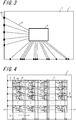
- FIG. 4 shows a block circuit diagram of the basic configuration of a display device underlying the display device according to the disclosure.
- FIG. 5 shows a sectional view taken along the line A1-A2 of FIG. 4 .
- the display device includes: a glass substrate 1; scanning signal lines 2 each arranged in a predetermined direction (row direction, for example) on the glass substrate 1; light emission-control signal lines 3 which intersect the scanning signal lines 2 and each of which is arranged in a direction perpendicular to the predetermined direction (column direction, for example); an effective region 11 including a plurality of pixel portions (Pmn) demarcated by the scanning signal lines 2 and the light emission-control signal lines 3; and a plurality of light emitting elements 14 disposed on an insulating layer.
- the scanning signal lines 2 and the light emission-control signal lines 3 are connected to back wiring 9 disposed on a back surface of the glass substrate 1 via a side wiring disposed on the side surface of the glass substrate 1.
- the back wiring 9 is connected to a drive element 6, such as an IC or an LSI, disposed on the back surface of the glass substrate 1. That is, in the display device, drive control for display is carried out by the drive element 6 disposed on the back surface of the glass substrate 1.
- the drive element 6 is mounted on the back-surface side of the glass substrate 1 by means of COG (Chip On Glass) or otherwise.
- each pixel portion 15 there is disposed a light emission-control section 22 for control of the light emitting element 14 (LDmn) located in a light emission region (Lmn) in respect of light-emission mode, non-light-emission mode, and light-emission intensity.
- the light emission-control section 22 includes a TFT (Thin Film Transistor) 12 (shown in FIG. 6 ) which serves as a switching element for inputting a light emission signal to the corresponding light emitting element 14, and a TFT 13 (shown in FIG.
- a drive element which serves as a drive element for effecting current drive to the light emitting element 14 on the basis of a potential difference (light emission signal) between a positive voltage (anode voltage of about 3 to 5 V) and a negative voltage (cathode voltage of about -3 to 0 V) according to the level (voltage) of a light emission-control signal (a signal which is transmitted through the light emission-control signal line 3).
- a capacitive element On a connection line for providing connection between a gate electrode and a source electrode in the TFT 13, a capacitive element is disposed, and the capacitive element serves as a retention capacitance that retains the voltage of the light emission-control signal inputted to the gate electrode of the TFT 13 over a certain period of time until initiation of succeeding reprogramming operation (one-frame period).
- the light emitting element 14 is electrically connected to the light emission-control section 22, a positive voltage input line 16, and a negative voltage input line 17 via through conductors 23a and 23b, such as through holes, passing through an insulating layer 41 (shown in FIG. 5 ) disposed in the effective region 11. That is, a positive electrode of the light emitting element 14 is connected to the positive voltage input line 16 via the through conductor 23a and the light emission-control section 22, whereas a negative electrode of the light emitting element 14 is connected to the negative voltage input line 17 via the through conductor 23b.
- the display device includes a fringe part 1g, which has no involvement with display action, located between the effective region 11 and the edge of the glass substrate 1, and a light emission-control signal line drive circuit, a scanning signal line drive circuit, etc. may occasionally be placed on the fringe part 1g. It is desired that the fringe part 1g have as small a width as possible.
- a plurality of glass substrates 1 are cut from a single base substrate. In order to suppress the influence of a cut line on the light emission-control section 22, there has been proposed an arrangement as shown in the block circuit diagram of FIG. 7 in which, in the outermost pixel portion 15, the light emission-control section 22 is located more inwardly than the light emitting element 14 in the glass substrate 1, as viewed in a plan view.
- Each pixel portion 15 may occasionally be formed of corresponding one of a sub-pixel portion for red light emission, a sub-pixel portion for green light emission, and a sub-pixel portion for blue light emission.
- the sub-pixel portion for red light emission includes a red light emitting element such as a red LED
- the sub-pixel portion for green light emission includes a green light emitting element such as a green LED
- the sub-pixel portion for blue light emission includes a blue light emitting element such as a blue LED.
- these sub-pixel portions are arranged in rows or columns.
- FIG. 8 is a fragmentary plan view showing the outermost pixel portion 15 (P11) in enlarged dimension in the display device shown in FIG. 7
- FIG. 9 is a sectional view taken along the line B1-B2 of FIG. 8 .
- a light-shielding member 25 made for example of a black matrix is disposed on the fringe part 1g.
- a resin-made insulating layer 51 which is a layer made of resin such as acrylic resin, is disposed on the glass substrate 1, and the light emitting element 14 is mounted on the resin-made insulating layer 51.
- the light emitting element 14 is located at a predetermined distance from the edge of the glass substrate 1.
- the light emitting element 14 mounted on the resin-made insulating layer 51 is electrically connected to a positive electrode 54a and a negative electrode 54b placed on the resin-made insulating layer 51 via an electroconductive connection member such as solder.
- the positive electrode 54a includes: an electrode layer 52a of, for example, Mo-Al-Mo layered configuration (made by successive laminations of an Al layer and a Mo layer on a Mo layer); and a transparent electrode 53a made of, for example, ITO (Indium Tin Oxide) that covers the electrode layer 52a.
- the negative electrode 54b includes: an electrode layer 52b of, for example, Mo-Al-Mo layered configuration; and a transparent electrode 53b made for example of ITO that covers the electrode layer 52b.
- an input electrode 2p is disposed, and the input electrode 2p includes: an electrode layer 52c; and a transparent electrode 53c made for example of ITO that covers the electrode layer 52c.
- the input electrode 2p is electrically connected to the positive electrode 54a, and functions as a relay electrode which is electrically connected to the back wiring 9 via a side wiring 60.
- An insulating layer 55 made of, for example, silicon oxide (SiO 2 ) or silicon nitride (SiN x ) is placed so as to cover the resin-made insulating layer 51, part of each of the transparent electrodes 53a and 53b (a part thereof not overlapping with the light emitting element 14), and the periphery of the transparent electrode 53c.
- a light-shielding layer 56 made for example of a black matrix is disposed on the insulating layer 55, except for the light emitting element 14 mounting area and the light-shielding member 25 placement area.
- the light-shielding layer 56 is intended to render the areas of the display device except at the light emitting element 14 dark-colored background areas, such as black background areas, as viewed in a plan view.
- the side wiring 60 which extends from a portion of the insulating layer 55 which covers the input electrode 2p as viewed in a plan view via the side surface of the glass substrate 1 to the back surface of the glass substrate 1 and which electrically connects the input electrode 2p and the back wiring 9.
- the side wiring 60 is formed through the application of an electroconductive paste containing electroconductive particles such as silver particles, with the subsequent firing process.
- a thick-film wiring board including a thick-film communication conductor serving as such a side wiring has been proposed to date (refer to Patent Literature 1, for instance).
- the light-shielding member 25 is placed so as to cover the input electrode 2p and the side wiring 60.
- the positive electrode of the light emitting element 14 is connected to the positive electrode 54a via an electroconductive connection member such as solder, and the negative electrode of the light emitting element 14 is connected to the negative electrode 54b via an electroconductive connection member such as solder.
- the light emitting element 14 is mounted on the glass substrate 1.
- a resin paste for forming the light-shielding member 25 that covers the side wiring 60 is applied so as to cover the input electrode 2p.
- the resin paste spreads over and beyond the input electrode 2p, and the end of the paste lies over an inward area of the glass substrate 1.
- the resin paste reaches other electrode such as an electrode for inspection which is disposed near the input electrode 2p and on an inward side of the glass substrate 1, which may cause impairment of electrical connection of the other electrode.
- structural components constituting the embodiments of the wiring board, the light emitting device, and the display device according to the disclosure only the main components are shown in each drawing to be hereafter referred to for the sake of explanation of the wiring board, the light emitting device, and the display device according to the disclosure.
- the wiring board, the light emitting device, and the display device according to the disclosure may therefore be provided with other known constituent components, although not shown in the drawings, such as a circuit board, a wiring conductor, a control IC, LSI, etc.
- FIGS. 4 to 9 in which the construction underlying the display device according to the disclosure is illustrated, for similar parts, and the detailed description of such parts will be omitted.
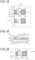
- FIGS. 1A and 1B are views showing one embodiment of the wiring board.
- FIG. 1A is a plan view showing electrodes and their surroundings
- FIG. 1B is a sectional view taken along the line C1-C2 of FIG. 1A .
- the wiring board includes: a glass substrate 1, as a base plate, including a first surface 1a, a second surface 1b which is opposite to the first surface 1a, and a side surface 1s; an input electrode 2p, as an electrode, located close to a side 1h of the first surface 1a; an insulating layer 55 disposed on the glass substrate 1; and a side wiring 60 disposed so as to extend from the input electrode 2p via the side surface 1s to the second surface 1b.
- An end 55h of the insulating layer 55 located close to the side 1h is provided with a cutaway portion 55a extending in an inward direction of the insulating layer 55.
- the input electrode 2p is disposed in an entrance 55ai-side part of the cutaway portion 55a, and the cutaway portion 55a includes a bottom-side part constituting an inward area 55ao which is free of the input electrode 2p.
- an inspection electrode 61 may occasionally be disposed near the input electrode 2p and close to a center of the glass substrate 1.
- the insulating layer 55 covers the four sides of the quadrangular inspection electrode 61, and an opening 55k uncovers the remainder of the inspection electrode 61.
- a resin paste for forming the light-shielding member 25 that covers the side wiring 60 is applied so as to cover the input electrode 2p.
- the resin paste spreads over and beyond the input electrode 2p, and the end of the paste lies over an inward area of the glass substrate 1.
- the resin paste reaches other electrode than the input electrode such as the inspection electrode which is disposed near the input electrode 2p and on an inward side of the glass substrate 1, which may cause impairment of electrical connection of the other electrode.
- the light-shielding member 25 can be restrained from reaching other constituent member than the input electrode 2p, such as the inspection electrode 61, which should avoid contact with the light-shielding member 25. That is, since the cutaway portion 55a includes the bottom-side part constituting the inward area 55ao which is free of the input electrode 2p, the resin paste which has entered the cutaway portion 55a is stored in the inward area 55ao. As a result, it is possible to restrain the resin paste from reaching the inspection electrode 61, etc.
- the input electrode 2p is disposed in the entrance 55ai-side part of the cutaway portion 55a, due to good wettability of the input electrode 2p to an electroconductive paste for forming the side wiring 60, the electroconductive paste is drawn into the cutaway portion 55a. As a result, an advantageous effect of satisfactory connection between the input electrode 2p and the side wiring 60 is also achieved.
- the glass substrate 1 provided as a base plate may be constructed of any of a plastic substrate, a ceramic substrate, and a metallic substrate, for example.
- the use of an insulating substrate such as a plastic substrate or a ceramic substrate is desirable from the standpoint of easiness in wiring formation.
- the substrate may be made in various shapes, including a quadrangular shape, a circular shape, an elliptical shape, and a trapezoidal shape.
- the input electrode 2p functions as a relay electrode which is connected to the side wiring 60, and includes, for example, a metallic layer of Mo-Al-Mo layered configuration (made by successive laminations of an Al layer and a Mo layer on a Mo layer); and a transparent conductor layer made of ITO (Indium Tin Oxide), etc. that covers the metallic layer.
- a metallic layer of Mo-Al-Mo layered configuration made by successive laminations of an Al layer and a Mo layer on a Mo layer
- ITO Indium Tin Oxide
- the input electrode 2p may be of a Mo-Al-Mo-ITO layer form as described above, or more preferably of metallic layer form such as Al-layer form, Al-Ti layer form, Ti-Al-Ti layer form, Mo-layer form, Mo-Al-Mo layer form, Cu-layer form, Cr-layer form, Ni-layer form, or Ag-layer form.
- the insulating layer 55 is formed of an inorganic insulating layer such as a silicon oxide (SiO 2 ) layer or a silicon nitride (SiN x ) layer, or of an organic insulating layer such as an acrylic resin layer or a polycarbonate layer.
- an inorganic insulating layer such as a silicon oxide (SiO 2 ) layer or a silicon nitride (SiN x ) layer
- an organic insulating layer such as an acrylic resin layer or a polycarbonate layer.
- the insulating layer 55 is disposed on a surface different from a surface where the input electrode 2p is placed, or disposed on a layer different from another insulating layer where the input electrode 2p is placed, a height of the insulating layer 55 is greater than a height of the input electrode 2p.
- the side wiring 60 may be formed through the application of an electroconductive paste composed of a paste component in liquid form such as alcohol, water, or an uncured resin component blended with electroconductive particles such as silver particles, gold particles, copper particles, aluminum particles, or stainless steel particles, with the subsequent firing process. Moreover, a part of the side surface 1s of the glass substrate 1 which bears the side wiring 60 may be provided with a groove. In this case, the resin paste finds its way smoothly into the groove in the desired location of the side surface 1s. As above described, it is desirable to form the side wiring 60 through the application of an electroconductive paste containing electroconductive particles, with the subsequent firing process. In this case, the resulting side wiring 60 tends to include a roughened surface with asperities or irregularities derived from the electroconductive particles. The roughened surface of the side wiring 60 has the effect of restraining the resin paste from running toward the inward area 55ao of the cutaway portion 55a.
- the entrance 55ai-side part of the cutaway portion 55a includes a widened area 55ak.
- the input electrode 2p being made of a material having good wettability to the electroconductive paste, facilitates the drawing of the electroconductive paste into the cutaway portion 55a, ensuring enhanced connection of the side wiring 60.
- the width of the widened area 55ak is adjusted in the range of 1.1 times to twice the width of the entrance 55ai.
- the input electrode 2p is entirely received in the cutaway portion 55a.
- a gap is provided between the input electrode 2p and the cutaway portion 55a.
- the wettability of the electroconductive paste becomes lower than the wettability of the input electrode 2p.
- the end 55h of the insulating layer 55 does not reach the side surface 1s.
- a part of the first surface 1a located between the end 55h of the insulating layer 55 and the side surface 1s serves as the path of the running resin paste and also as a reservoir for the resin paste, and in addition, the end 55h of the insulating layer 55 serves as a shoulder (dam) for the resin paste. Accordingly, it is possible to restrain superfluous resin paste from reaching the inspection electrode 61.
- the inward area 55ao of the cutaway portion 55a includes an extended part 55ae extending in a direction 1hd parallel to the side 1h.
- the inward area 55ao increases in size (inner volumetric capacity) and thus grows in performance capability as the reservoir for the resin paste. In consequence, it is possible to further restrain superfluous resin paste from reaching the inspection electrode 61.
- the inward area 55ao including the extended part 55ae may be at least partly curvilinear, such as circular, elliptic, or oblong, in a planar configuration. This configuration can effectively restrain superfluous resin paste from spreading out of the inward area 55ao, and thus achieves an advantageous effect that the performance of the inward area 55ao as the reservoir is further improved.
- the cutaway portion 55a may be defined by an area in which the insulating layer 55 is not formed. In this case, the cutaway portion 55a has a maximum depth, and it is possible to further restrain superfluous resin paste from reaching the inspection electrode 61.
- the input electrode 2p may be disposed on the remaining insulating layer 55.
- the lower part of the cutaway portion 55a contains a component which is the same as or analogous to that constituting the resin paste, and thus exhibits higher wettability to the resin paste. This increases the effect of drawing the resin paste into the cutaway portion 55a.
- the entrance 55ai-side part of the cutaway portion 55a includes a widened area 55ak, and also the inward area 55ao of the cutaway portion 55a includes an extended part 55ae extending in a direction 1hd parallel to the side 1h.
- the widened area 55ak may have a funnel-like shape defined by two straight line segments inclined relative to the side of the end of the insulating layer 5.
- the widened area 55ak has a taper whose width is gradually decreased from the entrance-side part toward the bottom-side part of the cutaway portion 55a, and thus has the effect of facilitating the drawing of the electroconductive paste into the cutaway portion 55a.
- a plurality of cutaway portions 55a are provided, and their extended parts 55ae are connected.
- the resin paste running through the cutaway portion 55a collects in the extended part 55ae while being restrained against further movement, and consequently, it is possible to further restrain superfluous resin paste from reaching the inspection electrode 61.
- the extended part 55ae may include a bulge area expanding in the inward direction and/or an opposite direction to the inward direction. This configuration provides greater facility for the resin paste to collect in the extended part 55ae.
- the bulge area may be curvilinear, such as partially circular, partially elliptic, or partially oblong, in a planar configuration. This configuration increases the resin-paste storage effect.
- the extended part 55ae may be defined by an area in which the insulating layer 55 is formed. In this case, the extended part 55ae has a maximum depth, and it is possible to further restrain superfluous resin paste from reaching the inspection electrode 61.
- the cutaway portion 55a measures about 1 ⁇ m to 100 ⁇ m in depth, about 5 ⁇ m to 500 ⁇ m in width, and about 100 ⁇ m to 1000 ⁇ m in length in the inward direction.
- the extended part 55ae measures about 1 ⁇ m to 100 ⁇ m in depth, and about 50 ⁇ m to 1000 ⁇ m in width.
- the light emitting device according to the disclosure is designed as a light emitting device including the wiring board according to the disclosure, the light emitting element 14 (as shown in FIGS. 4 to 9 ) which is connected to the input electrode 2p and is located on the first surface 1a, and the drive section 6 which is connected to the light emitting element via the side wiring 60 and is located on the second surface 1b.
- Examples of light emitting elements that may be used for the light emitting element 14 of the light emitting device include self-luminous light emitting elements such as a light emitting diode (LED) in microchip form, a monolithic light emitting diode, an organic EL, an inorganic EL, and a semiconductor laser device.
- the back wiring 9 connected to the side wiring 60 is disposed on the second surface (back surface) 1b of the glass substrate 1.
- the back wiring 9 is connected to the drive element 6 serving as the drive section, such as an IC or an LSI, disposed on the second surface 1b of the glass substrate 1. That is, in the light emitting device, drive control for light emission is carried out by the drive element 6 disposed on the second surface 1b of the glass substrate 1.
- the drive element 6 is mounted on the second-surface 1b side of the glass substrate 1 by means of COG (Chip On Glass) or otherwise.
- the drive section is not limited to the drive element 6, but may be of, for example, a drive circuit substrate or a drive circuit constructed of a TFT includes an LTPS (Low-temperature Poly Silicon)-made semiconductor layer formed on the glass substrate 1.
- the light emitting device is used as an illumination device, a printer head, etc.
- the display device according to the disclosure is designed as a display device including the wiring board according to the disclosure, a plurality of light emitting elements 14 each of which is connected to the input electrode 2p, the plurality of light emitting elements 14 being arranged in a matrix on the first surface 1a, and the drive section which is connected to the plurality of light emitting elements 14 via the side wiring 60 and is located on the second surface 1b.
- Examples of light emitting elements that may be used for the light emitting element 14 of the display device include self-luminous light emitting elements such as a light emitting diode (LED) in microchip form, a monolithic light emitting diode, an organic EL, an inorganic EL, and a semiconductor laser device, and also elements of transmitted light-control type such as a unit liquid crystal display.
- LED light emitting diode
- the back wiring 9 connected to the side wiring 60 is disposed, and the back wiring 9 is connected to the drive element 6 serving as the drive section, such as an IC or an LSI, disposed on the second surface 1b of the glass substrate 1. That is, in the display device, drive control for light emission is carried out by the drive element 6 disposed on the second surface 1b of the glass substrate 1.
- the drive element 6 is mounted on the second-surface 1b side of the glass substrate 1 by means of COG (Chip On Glass) or otherwise.
- the drive section is not limited to the drive element 6, but may be of, for example, a drive circuit substrate or a drive circuit constructed of a TFT including an LTPS (Low-temperature Poly Silicon)-made semiconductor layer formed on the glass substrate 1.
- a large-sized combined display equipment, or so-called multifunction display may be constructed by arranging (tiling) a plurality of glass substrates 1, each equipped with the plurality of light emitting elements 14, in a matrix on the same plane, with their side surfaces joined together by an adhesive or the like.
- the glass substrate 1 may either be a transparent glass substrate or be an opaque substrate.
- the glass substrate 1 may be constructed of a colored glass substrate such as a black- or gray-colored substrate, or a ground glass-made glass substrate, or also a glass-ceramic composite substrate.
- the wiring board includes: a substrate including a first surface, a second surface which is opposite to the first surface, and a side surface; an electrode located close to a side of the first surface; an insulating layer disposed on the substrate; and a side wiring disposed so as to extend from the electrode via the side surface to the second surface, wherein an end of the insulating layer located close to the side is provided with a cutaway portion extending in an inward direction of the insulating layer, the electrode is disposed in an entrance-side part of the cutaway portion, and the cutaway portion includes a bottom-side part constituting an inward area which is free of the electrode.
- the entrance-side part of the cutaway portion includes a widened area.
- the electrode is entirely received in the cutaway portion.
- the end of the insulating layer does not reach the side surface.
- the inward area of the cutaway portion includes an extended part extending in a direction parallel to the side of the first surface.
- the light emitting device is designed as a light emitting device including the wiring board described above, a light emitting element which is connected to the electrode and is located on the first surface, and a drive section which is connected to the light emitting element via the side wiring and is located on the second surface.
- the display device is designed as a display device including the wiring board described above, a plurality of light emitting elements each of which is connected to the electrode, the plurality of light emitting elements being arranged in a matrix on the first surface, and a drive section which is connected to the plurality of light emitting elements via the side wiring and is located on the second surface.
- the wiring board according to the disclosure includes: the substrate including the first surface, the second surface which is opposite to the first surface, and the side surface; the electrode located close to the side of the first surface; the insulating layer disposed on the substrate; and the side wiring disposed so as to extend from the electrode via the side surface to the second surface, wherein the end of the insulating layer located close to the side is provided with the cutaway portion extending in an inward direction of the insulating layer, the electrode is disposed in the entrance-side part of the cutaway portion, and the cutaway portion includes the bottom-side part constituting the inward area which is free of the electrode.
- a resin paste, which forms a light-shielding member as an overcoat on the side wiring, can be restrained from reaching other constituent member than the input electrode, such as an inspection electrode, which should avoid contact with the paste. That is, since the cutaway portion includes the bottom-side part constituting the inward area which is free of the input electrode, the resin paste which has entered the cutaway portion is stored in the inward area. As a result, it is possible to restrain the resin paste from reaching the inspection electrode, etc. Moreover, since the electrode is disposed in the entrance-side part of the cutaway portion, due to good wettability of the electrode to an electroconductive paste for forming the side wiring, the electroconductive paste is drawn into the cutaway portion. As a result, an advantageous effect of satisfactory connection between the electrode and the side wiring is also achieved.
- the electrode made of a material having good wettability to the electroconductive paste for forming the side wiring facilitates the drawing of the electroconductive paste into the cutaway portion, ensuring enhanced connection of the side wiring.
- the electrode is entirely received in the cutaway portion, in the direction of movement of the electroconductive paste (in a direction from the entrance of the cutaway portion inward), a gap is provided between the electrode and the cutaway portion. In this gap, the wettability of the electroconductive paste becomes lower than the wettability of the electrode. As a result, it is possible to restrain the electroconductive paste from running rapidly from the entrance of the cutaway portion toward the inward area thereof, and restrain the electroconductive paste from entering the inward area to an excessive degree.
- the end of the insulating layer in the case where the end of the insulating layer do not reach the side surface when the side of the first surface is viewed in the plan view, a part of the first surface located between the end of the insulating layer and the side surface serves as the path of the running resin paste and also as a reservoir for the resin paste, and in addition, the end of the insulating layer serves as a shoulder (dam) for the resin paste. In consequence, it is possible to further restrain superfluous resin paste from reaching the inspection electrode.
- the inward area of the cutaway portion includes an extended part extending in a direction parallel to the side of the first surface
- the inward area increases in size (inner volumetric capacity) and thus grows in performance capability as the reservoir for the resin paste. In consequence, it is possible to further restrain superfluous resin paste from reaching the inspection electrode, etc.
- the light emitting device is designed as a light emitting device including the wiring board described above, a light emitting element which is connected to the electrode and is located on the first surface, and a drive section which is connected to the light emitting element via the side wiring and is located on the second surface. Accordingly, there is obtained the light emitting device in which connectivity of the side wiring is satisfactory and other electrode such as an inspection electrode is highly electrically reliable.
- the display device is designed as a display device including the wiring board described above, a plurality of light emitting elements each of which is connected to the electrode, the plurality of light emitting elements being arranged in a matrix on the first surface, and a drive section which is connected to the plurality of light emitting elements via the side wiring and is located on the second surface. Accordingly, there is obtained the display device in which connectivity of the side wiring is satisfactory and other electrode such as an inspection electrode is highly electrically reliable.
- the display device may be built as a self-luminous display device such as a LED display device or an organic EL display device, or a liquid crystal display device.
- the display device according to the disclosure is applicable to various types of an electronic device. Examples of the electronic device to which the display device is applicable include a large-size combined display device (multifunction display), an automotive route guidance system (car navigation system), a route guidance system for boats and ships, a route guidance system for aircraft, a smartphone terminal, a mobile phone, a tablet terminal, a personal digital assistant (PDA), a video camera, a digital still camera, an electronic notepad, an electronic book, an electronic dictionary, a personal computer, a copier, a video-game machine terminal, a television set, a product indication tag, a price indication tag, an industrial programmable display device, a car audio device, a digital audio player, a facsimile, a printer, an automated teller machine (ATM), a vending machine, a head-mounted display (HMD),
- ATM automated
Landscapes
- Engineering & Computer Science (AREA)
- Manufacturing & Machinery (AREA)
- Microelectronics & Electronic Packaging (AREA)
- Devices For Indicating Variable Information By Combining Individual Elements (AREA)
- Led Device Packages (AREA)
- Electroluminescent Light Sources (AREA)
- Non-Metallic Protective Coatings For Printed Circuits (AREA)
- Structure Of Printed Boards (AREA)
- Printing Elements For Providing Electric Connections Between Printed Circuits (AREA)
Applications Claiming Priority (2)
| Application Number | Priority Date | Filing Date | Title |
|---|---|---|---|
| JP2018243165 | 2018-12-26 | ||
| PCT/JP2019/046599 WO2020137342A1 (ja) | 2018-12-26 | 2019-11-28 | 配線基板、それを用いた発光装置及び表示装置 |
Publications (2)
| Publication Number | Publication Date |
|---|---|
| EP3905850A1 true EP3905850A1 (de) | 2021-11-03 |
| EP3905850A4 EP3905850A4 (de) | 2022-09-21 |
Family
ID=71127841
Family Applications (1)
| Application Number | Title | Priority Date | Filing Date |
|---|---|---|---|
| EP19902436.5A Withdrawn EP3905850A4 (de) | 2018-12-26 | 2019-11-28 | Leiterplatte und lichtemittierende vorrichtung und anzeigevorrichtung mit verwendung davon |
Country Status (5)
| Country | Link |
|---|---|
| US (1) | US11984547B2 (de) |
| EP (1) | EP3905850A4 (de) |
| JP (2) | JP7204782B2 (de) |
| CN (1) | CN113196879B (de) |
| WO (1) | WO2020137342A1 (de) |
Families Citing this family (4)
| Publication number | Priority date | Publication date | Assignee | Title |
|---|---|---|---|---|
| US11473756B2 (en) * | 2018-09-20 | 2022-10-18 | Schreder S.A. | Light emitting device with adaptable glare class |
| WO2021186058A1 (en) * | 2020-03-19 | 2021-09-23 | Schreder S.A. | Light emitting device with adaptable glare class |
| WO2022054943A1 (ja) * | 2020-09-14 | 2022-03-17 | Agc株式会社 | Led素子用基板および画像表示装置 |
| KR20240106174A (ko) * | 2022-12-29 | 2024-07-08 | 엘지디스플레이 주식회사 | 표시 장치 |
Family Cites Families (13)
| Publication number | Priority date | Publication date | Assignee | Title |
|---|---|---|---|---|
| JP3048722B2 (ja) * | 1991-12-04 | 2000-06-05 | 日本シイエムケイ株式会社 | プリント配線板 |
| JP2001033802A (ja) * | 1999-07-15 | 2001-02-09 | Rohm Co Ltd | 液晶表示モジュール |
| TW535352B (en) * | 2000-05-30 | 2003-06-01 | Alps Electric Co Ltd | Surface-mounting type electronic circuit unit |
| JP2003078226A (ja) * | 2001-08-31 | 2003-03-14 | Noritake Co Ltd | 厚膜配線基板およびその製造方法 |
| JP4579074B2 (ja) * | 2005-07-15 | 2010-11-10 | 三菱電機株式会社 | フレキシブル回路基板及びこれを用いた表示装置 |
| JP2008135574A (ja) * | 2006-11-28 | 2008-06-12 | Kyocera Corp | 配線基板およびそれを用いた半導体装置とプローブカード |
| JP2012074478A (ja) * | 2010-09-28 | 2012-04-12 | Asahi Glass Co Ltd | 発光素子用基板および発光装置 |
| JP6128209B2 (ja) * | 2013-04-26 | 2017-05-17 | 株式会社村田製作所 | 多層配線基板及びその製造方法並びにプローブカード用基板 |
| JP6305759B2 (ja) * | 2013-12-26 | 2018-04-04 | 株式会社ジャパンディスプレイ | 表示装置 |
| JP2015133394A (ja) * | 2014-01-10 | 2015-07-23 | 住友電工プリントサーキット株式会社 | プリント回路板、及びプリント回路板の製造方法 |
| EP3282488A4 (de) * | 2015-04-22 | 2018-05-02 | Toppan Printing Co., Ltd. | Dünnschichttransistoranordnungsformungssubstrat, bildanzeigevorrichtungssubstrat und dünnschichttransistoranordnungsformungssubstratherstellungsverfahren |
| KR20170059523A (ko) * | 2015-11-20 | 2017-05-31 | 삼성디스플레이 주식회사 | 표시 장치, 타일형 표시 장치 및 이의 제조 방법 |
| KR102612998B1 (ko) * | 2016-12-30 | 2023-12-11 | 엘지디스플레이 주식회사 | 표시 장치 및 이를 이용한 멀티 스크린 표시 장치 |
-
2019
- 2019-11-28 US US17/312,870 patent/US11984547B2/en active Active
- 2019-11-28 WO PCT/JP2019/046599 patent/WO2020137342A1/ja not_active Ceased
- 2019-11-28 JP JP2020562968A patent/JP7204782B2/ja active Active
- 2019-11-28 EP EP19902436.5A patent/EP3905850A4/de not_active Withdrawn
- 2019-11-28 CN CN201980083843.3A patent/CN113196879B/zh active Active
-
2022
- 2022-12-28 JP JP2022212762A patent/JP7449360B2/ja active Active
Also Published As
| Publication number | Publication date |
|---|---|
| US11984547B2 (en) | 2024-05-14 |
| US20220045250A1 (en) | 2022-02-10 |
| WO2020137342A1 (ja) | 2020-07-02 |
| JP7204782B2 (ja) | 2023-01-16 |
| JPWO2020137342A1 (ja) | 2021-11-04 |
| CN113196879A (zh) | 2021-07-30 |
| JP7449360B2 (ja) | 2024-03-13 |
| CN113196879B (zh) | 2024-04-23 |
| EP3905850A4 (de) | 2022-09-21 |
| JP2023057554A (ja) | 2023-04-21 |
Similar Documents
| Publication | Publication Date | Title |
|---|---|---|
| US11600240B2 (en) | Display apparatus with pixel structure on glass substrate and glass substrate | |
| KR102734994B1 (ko) | 표시장치 | |
| EP3432379B1 (de) | Anzeigevorrichtung | |
| US11984547B2 (en) | Wiring board, and light emitting device and display device using same | |
| KR102626953B1 (ko) | 유기발광 표시장치 | |
| US9136443B2 (en) | Display device and manufacturing method of the same | |
| KR102745684B1 (ko) | 터치 스크린 일체형 발광 표시 장치 | |
| KR102764385B1 (ko) | 표시장치 | |
| JP6856472B2 (ja) | 表示装置 | |
| KR102514439B1 (ko) | 유기발광 표시장치 | |
| KR20190056477A (ko) | 표시 장치 | |
| KR20190070038A (ko) | 배선 필름 및 그를 포함한 표시 장치 | |
| US11678507B2 (en) | Display apparatus having a crack resistant structure | |
| KR20160140074A (ko) | 유기발광 표시장치 | |
| CN115004389B (zh) | 显示装置以及显示装置的制造方法 | |
| WO2021024722A1 (ja) | 表示装置 | |
| KR20170079156A (ko) | 유기발광 표시장치 | |
| JP2014145919A (ja) | 表示装置 | |
| KR20230088995A (ko) | 터치표시장치 | |
| EP4703856A1 (de) | Anzeigevorrichtung | |
| KR102788206B1 (ko) | 플렉서블 디스플레이 장치 및 이의 제조 방법 | |
| CN118742139A (zh) | 显示装置 | |
| KR20250063968A (ko) | 표시 장치 | |
| CN119855410A (zh) | 显示装置 |
Legal Events
| Date | Code | Title | Description |
|---|---|---|---|
| STAA | Information on the status of an ep patent application or granted ep patent |
Free format text: STATUS: THE INTERNATIONAL PUBLICATION HAS BEEN MADE |
|
| PUAI | Public reference made under article 153(3) epc to a published international application that has entered the european phase |
Free format text: ORIGINAL CODE: 0009012 |
|
| STAA | Information on the status of an ep patent application or granted ep patent |
Free format text: STATUS: REQUEST FOR EXAMINATION WAS MADE |
|
| 17P | Request for examination filed |
Effective date: 20210603 |
|
| AK | Designated contracting states |
Kind code of ref document: A1 Designated state(s): AL AT BE BG CH CY CZ DE DK EE ES FI FR GB GR HR HU IE IS IT LI LT LU LV MC MK MT NL NO PL PT RO RS SE SI SK SM TR |
|
| DAV | Request for validation of the european patent (deleted) | ||
| DAX | Request for extension of the european patent (deleted) | ||
| REG | Reference to a national code |
Ref country code: DE Ref legal event code: R079 Free format text: PREVIOUS MAIN CLASS: H05B0033060000 Ipc: H05K0003400000 |
|
| A4 | Supplementary search report drawn up and despatched |
Effective date: 20220823 |
|
| RIC1 | Information provided on ipc code assigned before grant |
Ipc: G09G 3/32 20160101ALN20220817BHEP Ipc: H01L 25/16 20060101ALN20220817BHEP Ipc: H05K 1/18 20060101ALN20220817BHEP Ipc: H05K 1/03 20060101ALN20220817BHEP Ipc: H05B 45/30 20200101ALI20220817BHEP Ipc: H01L 33/62 20100101ALI20220817BHEP Ipc: H01L 25/075 20060101ALI20220817BHEP Ipc: H05K 3/40 20060101AFI20220817BHEP |
|
| P01 | Opt-out of the competence of the unified patent court (upc) registered |
Effective date: 20230505 |
|
| STAA | Information on the status of an ep patent application or granted ep patent |
Free format text: STATUS: THE APPLICATION HAS BEEN WITHDRAWN |
|
| 18W | Application withdrawn |
Effective date: 20250808 |