EP3874590B1 - Dual supply low-side gate driver - Google Patents
Dual supply low-side gate driver Download PDFInfo
- Publication number
- EP3874590B1 EP3874590B1 EP19879052.9A EP19879052A EP3874590B1 EP 3874590 B1 EP3874590 B1 EP 3874590B1 EP 19879052 A EP19879052 A EP 19879052A EP 3874590 B1 EP3874590 B1 EP 3874590B1
- Authority
- EP
- European Patent Office
- Prior art keywords
- node
- coupled
- driver
- circuit
- driver circuit
- Prior art date
- Legal status (The legal status is an assumption and is not a legal conclusion. Google has not performed a legal analysis and makes no representation as to the accuracy of the status listed.)
- Active
Links
Images


Classifications
-
- H—ELECTRICITY
- H02—GENERATION; CONVERSION OR DISTRIBUTION OF ELECTRIC POWER
- H02M—APPARATUS FOR CONVERSION BETWEEN AC AND AC, BETWEEN AC AND DC, OR BETWEEN DC AND DC, AND FOR USE WITH MAINS OR SIMILAR POWER SUPPLY SYSTEMS; CONVERSION OF DC OR AC INPUT POWER INTO SURGE OUTPUT POWER; CONTROL OR REGULATION THEREOF
- H02M1/00—Details of apparatus for conversion
- H02M1/08—Circuits specially adapted for the generation of control voltages for semiconductor devices incorporated in static converters
-
- G—PHYSICS
- G05—CONTROLLING; REGULATING
- G05F—SYSTEMS FOR REGULATING ELECTRIC OR MAGNETIC VARIABLES
- G05F1/00—Automatic systems in which deviations of an electric quantity from one or more predetermined values are detected at the output of the system and fed back to a device within the system to restore the detected quantity to its predetermined value or values, i.e. retroactive systems
- G05F1/10—Regulating voltage or current
- G05F1/46—Regulating voltage or current wherein the variable actually regulated by the final control device is DC
- G05F1/56—Regulating voltage or current wherein the variable actually regulated by the final control device is DC using semiconductor devices in series with the load as final control devices
-
- H—ELECTRICITY
- H02—GENERATION; CONVERSION OR DISTRIBUTION OF ELECTRIC POWER
- H02M—APPARATUS FOR CONVERSION BETWEEN AC AND AC, BETWEEN AC AND DC, OR BETWEEN DC AND DC, AND FOR USE WITH MAINS OR SIMILAR POWER SUPPLY SYSTEMS; CONVERSION OF DC OR AC INPUT POWER INTO SURGE OUTPUT POWER; CONTROL OR REGULATION THEREOF
- H02M1/00—Details of apparatus for conversion
- H02M1/08—Circuits specially adapted for the generation of control voltages for semiconductor devices incorporated in static converters
- H02M1/088—Circuits specially adapted for the generation of control voltages for semiconductor devices incorporated in static converters for the simultaneous control of series or parallel connected semiconductor devices
-
- H—ELECTRICITY
- H02—GENERATION; CONVERSION OR DISTRIBUTION OF ELECTRIC POWER
- H02M—APPARATUS FOR CONVERSION BETWEEN AC AND AC, BETWEEN AC AND DC, OR BETWEEN DC AND DC, AND FOR USE WITH MAINS OR SIMILAR POWER SUPPLY SYSTEMS; CONVERSION OF DC OR AC INPUT POWER INTO SURGE OUTPUT POWER; CONTROL OR REGULATION THEREOF
- H02M3/00—Conversion of DC power input into DC power output
- H02M3/02—Conversion of DC power input into DC power output without intermediate conversion into AC
- H02M3/04—Conversion of DC power input into DC power output without intermediate conversion into AC by static converters
- H02M3/10—Conversion of DC power input into DC power output without intermediate conversion into AC by static converters using discharge tubes with control electrode or semiconductor devices with control electrode
- H02M3/145—Conversion of DC power input into DC power output without intermediate conversion into AC by static converters using discharge tubes with control electrode or semiconductor devices with control electrode using devices of a triode or transistor type requiring continuous application of a control signal
- H02M3/155—Conversion of DC power input into DC power output without intermediate conversion into AC by static converters using discharge tubes with control electrode or semiconductor devices with control electrode using devices of a triode or transistor type requiring continuous application of a control signal using semiconductor devices only
- H02M3/156—Conversion of DC power input into DC power output without intermediate conversion into AC by static converters using discharge tubes with control electrode or semiconductor devices with control electrode using devices of a triode or transistor type requiring continuous application of a control signal using semiconductor devices only with automatic control of output voltage or current, e.g. switching regulators
-
- H—ELECTRICITY
- H02—GENERATION; CONVERSION OR DISTRIBUTION OF ELECTRIC POWER
- H02M—APPARATUS FOR CONVERSION BETWEEN AC AND AC, BETWEEN AC AND DC, OR BETWEEN DC AND DC, AND FOR USE WITH MAINS OR SIMILAR POWER SUPPLY SYSTEMS; CONVERSION OF DC OR AC INPUT POWER INTO SURGE OUTPUT POWER; CONTROL OR REGULATION THEREOF
- H02M3/00—Conversion of DC power input into DC power output
- H02M3/22—Conversion of DC power input into DC power output with intermediate conversion into AC
- H02M3/24—Conversion of DC power input into DC power output with intermediate conversion into AC by static converters
- H02M3/28—Conversion of DC power input into DC power output with intermediate conversion into AC by static converters using discharge tubes with control electrode or semiconductor devices with control electrode to produce the intermediate AC
- H02M3/325—Conversion of DC power input into DC power output with intermediate conversion into AC by static converters using discharge tubes with control electrode or semiconductor devices with control electrode to produce the intermediate AC using devices of a triode or a transistor type requiring continuous application of a control signal
- H02M3/335—Conversion of DC power input into DC power output with intermediate conversion into AC by static converters using discharge tubes with control electrode or semiconductor devices with control electrode to produce the intermediate AC using devices of a triode or a transistor type requiring continuous application of a control signal using semiconductor devices only
- H02M3/33507—Conversion of DC power input into DC power output with intermediate conversion into AC by static converters using discharge tubes with control electrode or semiconductor devices with control electrode to produce the intermediate AC using devices of a triode or a transistor type requiring continuous application of a control signal using semiconductor devices only with automatic control of the output voltage or current, e.g. flyback converters
-
- H—ELECTRICITY
- H03—ELECTRONIC CIRCUITRY
- H03K—PULSE TECHNIQUE
- H03K17/00—Electronic switching or gating, i.e. not by contact-making and –breaking
- H03K17/04—Modifications for accelerating switching
- H03K17/041—Modifications for accelerating switching without feedback from the output circuit to the control circuit
- H03K17/0412—Modifications for accelerating switching without feedback from the output circuit to the control circuit by measures taken in the control circuit
- H03K17/04123—Modifications for accelerating switching without feedback from the output circuit to the control circuit by measures taken in the control circuit in field-effect transistor switches
-
- H—ELECTRICITY
- H03—ELECTRONIC CIRCUITRY
- H03K—PULSE TECHNIQUE
- H03K17/00—Electronic switching or gating, i.e. not by contact-making and –breaking
- H03K17/16—Modifications for eliminating interference voltages or currents
- H03K17/161—Modifications for eliminating interference voltages or currents in field-effect transistor switches
- H03K17/162—Modifications for eliminating interference voltages or currents in field-effect transistor switches without feedback from the output circuit to the control circuit
-
- H—ELECTRICITY
- H02—GENERATION; CONVERSION OR DISTRIBUTION OF ELECTRIC POWER
- H02M—APPARATUS FOR CONVERSION BETWEEN AC AND AC, BETWEEN AC AND DC, OR BETWEEN DC AND DC, AND FOR USE WITH MAINS OR SIMILAR POWER SUPPLY SYSTEMS; CONVERSION OF DC OR AC INPUT POWER INTO SURGE OUTPUT POWER; CONTROL OR REGULATION THEREOF
- H02M1/00—Details of apparatus for conversion
- H02M1/0003—Details of control, feedback or regulation circuits
-
- H—ELECTRICITY
- H02—GENERATION; CONVERSION OR DISTRIBUTION OF ELECTRIC POWER
- H02M—APPARATUS FOR CONVERSION BETWEEN AC AND AC, BETWEEN AC AND DC, OR BETWEEN DC AND DC, AND FOR USE WITH MAINS OR SIMILAR POWER SUPPLY SYSTEMS; CONVERSION OF DC OR AC INPUT POWER INTO SURGE OUTPUT POWER; CONTROL OR REGULATION THEREOF
- H02M3/00—Conversion of DC power input into DC power output
- H02M3/02—Conversion of DC power input into DC power output without intermediate conversion into AC
- H02M3/04—Conversion of DC power input into DC power output without intermediate conversion into AC by static converters
- H02M3/10—Conversion of DC power input into DC power output without intermediate conversion into AC by static converters using discharge tubes with control electrode or semiconductor devices with control electrode
- H02M3/145—Conversion of DC power input into DC power output without intermediate conversion into AC by static converters using discharge tubes with control electrode or semiconductor devices with control electrode using devices of a triode or transistor type requiring continuous application of a control signal
- H02M3/155—Conversion of DC power input into DC power output without intermediate conversion into AC by static converters using discharge tubes with control electrode or semiconductor devices with control electrode using devices of a triode or transistor type requiring continuous application of a control signal using semiconductor devices only
- H02M3/156—Conversion of DC power input into DC power output without intermediate conversion into AC by static converters using discharge tubes with control electrode or semiconductor devices with control electrode using devices of a triode or transistor type requiring continuous application of a control signal using semiconductor devices only with automatic control of output voltage or current, e.g. switching regulators
- H02M3/158—Conversion of DC power input into DC power output without intermediate conversion into AC by static converters using discharge tubes with control electrode or semiconductor devices with control electrode using devices of a triode or transistor type requiring continuous application of a control signal using semiconductor devices only with automatic control of output voltage or current, e.g. switching regulators including plural semiconductor devices as final control devices for a single load
- H02M3/1588—Conversion of DC power input into DC power output without intermediate conversion into AC by static converters using discharge tubes with control electrode or semiconductor devices with control electrode using devices of a triode or transistor type requiring continuous application of a control signal using semiconductor devices only with automatic control of output voltage or current, e.g. switching regulators including plural semiconductor devices as final control devices for a single load comprising at least one synchronous rectifier element
-
- H—ELECTRICITY
- H03—ELECTRONIC CIRCUITRY
- H03K—PULSE TECHNIQUE
- H03K2217/00—Indexing scheme related to electronic switching or gating, i.e. not by contact-making or -breaking covered by H03K17/00
- H03K2217/0081—Power supply means, e.g. to the switch driver
Definitions
- Power supplies and power converters are used in a variety of electronic systems. Electrical power is generally transmitted over long distances as an alternating current (AC) signal. The AC signal is divided and metered as desired for each business or home location, and is often converted to direct current (DC) for use with individual electronic devices or components. Modern electronic systems often employ devices or components designed to operate using different DC voltages. Accordingly, different DC-DC converters, or a DC-DC converter that supports a wide range of output voltages, are needed for such systems.
- AC alternating current
- DC direct current
- DC-DC converter topologies exist. An example can be seen in the document US 2014/210445 A1 . The available topologies differ with regard to the components used, the amount of power handled, the input voltage(s), the output voltage(s), efficiency, reliability, size and/or other characteristics.
- One example DC-DC converter topology uses a secondary low voltage "BIAS" input that is driven by the output voltage or an auxiliary power supply. This option improves efficiency at the cost of additional components and increased topology size. Efforts to improve DC-DC converter topologies are ongoing.
- an automotive system comprises a first regulator configured to provide a first output voltage based on a first input voltage level.
- the system also comprises a second regulator configured to provide a second output voltage based on a second input voltage level.
- the system also comprises a first driver circuit coupled to the first regulator and a switch, wherein the first driver circuit is configured to drive the switch based on the first output voltage.
- the system also comprises a second driver circuit coupled to the second regulator and the switch, wherein the second driver circuit is configured to drive the switch based on the second output voltage.
- the system also comprises a driver controller coupled to the first driver circuit and the second driver circuit, wherein the driver controller is configured to select one of the first driver circuit and the second driver circuit to drive the switch based on a control signal.
- the system also comprises a switch node coupled to the switch, wherein a switch node voltage at the switch node is a function of the switch being turned on and off.
- the system also comprises a load coupled to the switch node.
- a circuit comprises a first regulator configured to provide a first output voltage based on a first input voltage level.
- the circuit also comprises a second regulator configured to provide a second output voltage based on a second input voltage level, wherein the second input voltage level is lower than the first input voltage level.
- the circuit also comprises a first driver circuit coupled to the first regulator, wherein the first driver circuit is configured to provide a first gate drive signal based on the first output voltage.
- the circuit also comprises a second driver circuit coupled to the second regulator, wherein the second driver circuit is configured to provide a second gate drive signal based on the second output voltage.
- the circuit also comprises a driver controller coupled to the first driver circuit and the second driver circuit.
- the circuit also comprises a drive signal node coupled to an output node of the first driver circuit and an output node of the second driver circuit, wherein the driver controller is configured to select between the first driver circuit and the second driver circuit to provide a respective gate drive signal to the drive signal node.
- a dual supply gate driver comprises a first regulator circuit coupled to a first input voltage node.
- the dual supply gate driver also comprises a second regulator circuit coupled to a second input voltage node.
- the dual supply gate driver also comprises a first driver circuit coupled to an output node of the first regulator circuit.
- the dual supply gate driver also comprises a second driver circuit coupled to an output node of the second regulator circuit.
- the dual supply gate driver also comprises a driver controller coupled to the first driver circuit and the second driver circuit.
- the dual supply gate driver also comprises a drive signal node coupled to an output node of the first driver circuit and an output node of the second driver circuit.
- a dual supply gate driver includes a first regulator circuit coupled to a first input voltage node, and a second regulator circuit coupled to a second input voltage node.
- the dual supply gate driver also includes a first driver circuit coupled to an output node of the first regulator circuit.
- the dual supply gate driver also includes a second driver circuit coupled to an output node of the second regulator circuit.
- the dual supply gate driver also includes a driver controller coupled to the first driver circuit and the second driver circuit.
- the dual supply gate driver also includes a drive signal node coupled to an output node of the first driver circuit and an output node of the second driver circuit.
- a dual supply gate driver is commercialized as a stand-alone integrated circuit (IC) or chip.
- a dual supply gate driver is combined with other circuits (e.g., a power switch and/or sense switch of a converter circuit, a load) in an IC, chip, a multi-die module (MDM), or a printed circuit board (PCB).
- MDM multi-die module
- PCB printed circuit board
- the drive signal for the switch of a switching converter is efficiently provided without an external capacitor (for providing the drive current).
- a dual supply gate driver is used to drive a low-side switch of a switching converter while providing efficiency, small size, and low cost compared to other gate drivers.
- FIG. 1 is a block diagram showing a system 100 in accordance with some examples.
- the system 100 comprises a first regulator circuit 102 and a second regulator circuit 104.
- the first regulator circuit 102 receives a first input voltage (V1) and provides a first output voltage (VO1) based on V1.
- the second regulator circuit 104 receives a second input voltage (V2) and provides a second output voltage (VO2) based on V2.
- VO1 is provided to a first driver circuit 108.
- the first driver circuit 108 is configured to provide a drive signal based on VO1 to a switch 114.
- the second driver circuit 110 is configured to provide a drive signal based on VO2 to the switch 114.
- the driver controller 112 selects the first driver circuit 108 or the second driver circuit 110 to provide the drive signal to the switch 114 based on a signal 124 from the voltage monitor circuit 106. Also, a signal (e.g., the SWITCH ON signal in FIG. 5 ) from a PWM controller (not shown) is used to determine when the driver controller 112 asserts CS1 or CS2. In the example of FIG. 1 , the voltage monitor circuit 106 is configured to monitor V2. When the signal 124 indicates that V2 is greater than a threshold, the driver controller 112 selects the second driver circuit 110 (using control signal "CS2") to provide the drive signal to the switch 114. On the other hand, when the signal 124 indicates that V2 is less than or equal to the threshold, the driver controller 112 selects the first driver circuit 108 (using control signal "CS1") to provide the drive signal to the switch 114.
- a signal e.g., the SWITCH ON signal in FIG. 5
- the voltage monitor circuit 106 is configured to monitor V
- the drive signal is provided to the switch 114 via a drive signal node 122.
- the drive signal node 122 corresponds to an output pin for a dual supply gate driver IC or chip that includes the first regulator circuit 102, the second regulator circuit 104, the voltage monitor circuit 106, the first driver 108, the second driver 110, and the driver controller 112.
- the on/off operations of the switch 114 change the voltage at node 120, which corresponds to a switch node.
- output component(s) 116 are coupled to the node 120.
- Examples of the output component(s) 116 include an output inductor and an output capacitor. Coupled to the output component(s) 116 is a load 118 powered by an output voltage (VOUT) that is based on the operations of the switch 114.
- VOUT output voltage
- the system 100 corresponds to an automotive system.
- the first regulator circuit 102 receives V1 (e.g., 5V-40V) from a battery or conditioning components (e.g., filters and/or regulators).
- V2 may be a bias voltage based on VOUT or a lower voltage auxiliary supply.
- dual supply gate driver components of FIG. 1 are part of a buck converter or buck converter controller to direct low-side switching operations, where VOUT is smaller than V1.
- Example VOUT levels include 5V, 3.3V, 1.8V, or 1.2V.
- multiple switching converters are used in an automotive system or other electrical systems to power different loads with different input voltage requirements.
- Example loads for an automotive system include, but are not limited to, microprocessors, sensors, actuators, displays, an infotainment interface, and an intelligent power module (IPM).
- IPM intelligent power module
- FIG. 2 is a schematic diagram showing a buck converter system 200 in accordance with some examples.
- the buck converter system 200 includes a step-down converter circuit 202 with an input supply voltage (VIN) node, a bias node, a switch (SW) node, a voltage supply (VCC) node, a feedback (FB) node.
- the SW node of step-down converter circuit 202 is coupled to the first end of an output inductor (LOUT).
- the second end of LOUT is coupled to the first (e.g., top) plate of an output capacitor (COUT).
- the second (e.g., bottom) plate of COUT is coupled to a ground node.
- VIN input supply voltage
- SW switch
- VCC voltage supply
- FB feedback
- the SW node of step-down converter circuit 202 is coupled to the first end of an output inductor (LOUT).
- the second end of LOUT is coupled to the first (e.g., top) plate of an output capacitor (COUT
- VOUT for the buck converter system 200 is provided to load (not shown) and a voltage divider formed using R1 and R2.
- the node 204 between R1 and R2 is coupled to the FB node for the step-down converter circuit 202.
- the step-down converter circuit 202 also receives VOUT at the bias node.
- the buck converter system 200 of FIG. 2 includes an external capacitor (C1) coupled to the VCC node of the step-down converter circuit 202, where VCC is the driver supply.
- FIG. 3 is a schematic diagram showing a flyback converter system 300 in accordance with some examples.
- the flyback converter system 300 includes a flyback converter circuit 302 with an input supply voltage (VIN) node, a switch (SW) node, a bias node, and a VCC node. More specifically, the switch node is coupled to a transformer 304. A first winding of the transformer 304 is coupled between an input supply voltage (VIN) and the SW node. A second winding of the transformer 403 is coupled between another voltage supply node 308 and the anode of a diode (D1). The cathode of D1 is coupled to the first (e.g., top) plate of an output capacitor (COUT). The second (e.g., bottom) plate of COUT is coupled to a voltage supply node 308 and the second winding.
- VIN input supply voltage
- SW switch
- the bias node is coupled to a circuit that includes a bias coil 306 inductively coupled to the transformer 304.
- the third winding 306 is coupled between a ground node and the anode of another diode (D2).
- the cathode of D2 is coupled to the bias node of the flyback converter circuit 302.
- the first (e.g., top) plate of a capacitor (C3) is coupled to the cathode of D2 and to the bias node.
- the second (e.g., bottom) plate of C3 is coupled to a ground node.
- the flyback converter system 300 includes an external capacitor (C2) coupled to the VCC node of the flyback converter circuit 302. More specifically, the first (e.g., top) plate of C2 is coupled to the VCC node of the flyback converter 300, and the second (e.g., bottom) plate of C2 is coupled to a ground node.
- the bias voltage is driven by the output voltage.
- the bias voltage is driven by the bias winding 306.
- the bias voltage provided to the step-down converter circuit 202 or the flyback converter circuit 302 can improve efficiency by diverting the chip bias current from VIN to a lower voltage supply that is efficiently generated.
- a low-side switch driver runs off of VCC, which is a regulated supply derived from either VIN or the bias voltage when available. Once the bias voltage exceeds a minimum required voltage, the VCC regulator will run all the driver current from the bias voltage.
- FIG. 4 is a schematic diagram showing a voltage regulator 400 for a low-side switch driver in accordance with some examples.
- the voltage regulator 400 comprises a current source 402 coupled to a VIN node 408.
- the voltage regulator 400 also includes a transistor (M1) with a control terminal, a first current terminal, and a second current terminal.
- the voltage regulator 400 also includes a diode (D3), where the anode of D3 is coupled to the current source 402, and the cathode of D3 is coupled to the control terminal of M1.
- the first current terminal of M1 is coupled to the VIN node 408.
- the second current terminal of M1 is coupled to the input node of a comparator 404.
- the other input node of the comparator 404 is a voltage reference (Ref), and the output of the comparator 404 is coupled to cathode of D3 and the control terminal of M1.
- the second current terminal of M1 is also coupled to a driver circuit 412 powered by the charge stored by an external capacitor (Cext) coupled to a VCC pin 406 (e.g., the VCC node of FIGS. 2 or 3 ).
- the driver circuit 412 includes a series of inverters 404, where the charge stored by Cext is provided to the inverters 414.
- Cext is charged by the voltage at the VIN node 408 through M1, or from a bias node 410 through a transistor (M2).
- M2 includes a control terminal coupled to a node 416 between the current source 402 and the anode of D3.
- the first current terminal of M3 is coupled to the bias node 410 via a diode (D4), where the anode of D4 is coupled to the bias node 410 and the cathode of D4 is coupled to the first current terminal of M2.
- the second current terminal of M2 is coupled to the driver circuit 412, the VCC pin 406, and the first (e.g., top) plate of Cext.
- the second (e.g., bottom) plate of Cext is coupled to a ground node.
- the voltage regulator 400 also includes a transistor (M3) coupled between the driver circuit 412 and a switch node (SW) pin 416. As shown, the control terminal of M3 is coupled to an output of the driver circuit 412. Also, the first current terminal of M3 is coupled to the SW pin 416. Also, the second current terminal of M3 is coupled to a ground node.
- M3 transistor
- SW switch node
- the driver circuit 412 is a low-side switch driver that runs off of VCC, which is a regulated supply derived from either the VIN voltage or the BIAS voltage when present. Once the BIAS voltage exceeds a minimum required voltage, the VCC regulator will run all the driver current from BIAS voltage. Cext is needed to ensure that the VCC rail remains well-regulated when the driver 412 switches and pulls very high peak currents from the VCC rail.
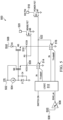
- FIG. 5 is a schematic diagram showing a dual supply gate driver circuit 500 in accordance with some examples.
- the dual supply gate driver circuit 500 comprises a first driver circuit 514 and a second driver circuit 516, where the output nodes of the first driver circuit 514 and the second driver circuit 516 are coupled to a drive signal node 522.
- a power transistor (M7) has its control terminal coupled to the drive signal node 522.
- the first current terminal of M7 is coupled to a switch node (SW) pin 518, and the second current terminal of M7 is coupled to a ground node.
- SW switch node
- the dual supply gate driver circuit 500 comprises a single IC with driver components (e.g., the first and second driver circuits 514 and 516), driver control components (e.g., the controller logic 512 and other components), and a power transistor (e.g., M7).
- driver components e.g., the first and second driver circuits 514 and 516
- driver control components e.g., the controller logic 512 and other components
- a power transistor e.g., M7
- the components represented for the dual supply gate driver circuit 500 correspond to multiple ICs (e.g., M7 is part of a first IC, while the driver components and driver control components are part of a second IC).
- the operations of the controller logic 512 are based on a control signal ("Switch ON") and a bias voltage level indicator signal ("BIAS ok").
- the BIAS_ok signal is provided by a comparator 506, where the output of the comparator 506 indicates when the BIAS voltage at node 508 is greater than a threshold.
- the controller logic 512 selects the second driver circuit 516 using a control signal ("Tri-stateB"), where the input signal (IN) to the second driver circuit 516 is buffered using a voltage supply signal (VCCB) based on the BIAS voltage available at node 508.
- VCCB is provided via a transistor (M5) having its first current terminal coupled to the node 508 via a diode (D5), which blocks the reverse path back to node 508 on start-up. If diode drop of D5 is too much, another option is to use a switch across D5, where the switch is closed when the BIAS voltage is sufficiently high.
- a lower BIAS voltage may be used. More specifically, the anode of D5 is coupled to the node 508 and the cathode of D5 is coupled to the first current terminal of M5. Also, the second current terminal of M5 is coupled to a VCCB node 510. Also, the control terminal of M5 is coupled to a current source 504 powered by the VIN voltage at node 502. As shown, the control terminal of the M5 is also coupled to the first end of a Zener diode (Z1) and the first (e.g., top) plate of a capacitor (C4). The second (e.g., bottom) plate of C4 and the second of Z1 are coupled to a ground node. With the arrangement of FIG.
- the voltage level at the VCCB node 510 is based on the BIAS voltage at node 508 and is provided to the second driver circuit 516.
- the controller logic 512 uses the second driver circuit 516 to provide the drive signal for M7.
- the controller logic 512 selects the first driver circuit 514 using a control signal ("Tri-stateA"), where the input signal (IN) to the first driver circuit 514 is buffered using a voltage supply signal (VCCA) based on the VIN voltage available at node 502.
- VCCA is provided via a transistor (M4) having its first current terminal coupled to the node 502.
- the second current terminal of M4 is coupled to a VCCA node 509.
- the control terminal of M4 is coupled to the current source 504 powered by the VIN voltage at node 502.
- the control terminal of the M4 is also coupled to Z1 and the first (e.g., top) plate of C4.
- M4 provides the same amount of current flow, but can handle a higher voltage relative to M5.
- the second (e.g., bottom) plate of C4 and the second of Z1 are coupled to a ground node.
- the voltage level at the VCCA node 509 is based on the VIN voltage at node 502 and is provided to the first driver circuit 514.
- the controller logic 512 uses the first driver circuit 514 to provide the drive signal for M7.
- the dual supply gate driver circuit 500 increases complexity compared to a single driver arrangement with the benefit of reducing power consumption (by using the BIAS voltage for power driver operations when the BIAS voltage is sufficiently high) for low-side switch drive operations. Also, the dual supply gate driver circuit 500 eliminates an external capacitor (to maintain VCC) and IC compared to other driver solutions.
- a sense transistor M6
- the control terminal for M6 is coupled to a resistor (R3) between the VCCA node 509 and the VCCB node 510.
- R3 corresponds to two resistors coupled in series, where the middle node is coupled to the of M6.
- the control terminal for M6 receives an average of the voltage levels at VCCA and VCCB.
- the second current terminal for M6 is coupled to a ground node
- the first current terminal for M6 is coupled to a sense node 520.
- the sense node 520 provides a signal used for feedback control and/or monitoring operations of a switching converter.
- the signal at the sense node 520 is provided to a pulse-switch modulation (PWM) controller coupled to the driver controller 112 of FIG. 1 .
- PWM pulse-switch modulation
- a PWM controller may use the signal at the sense node 520 to adjust a duty cycle and/or timing of the SWITCH_ON signal provided to the logic 512.
- FIG. 6 is a schematic diagram showing another dual supply gate driver 600 in accordance with some examples.
- the dual supply gate driver circuit 600 comprises a first driver circuit 614 and a second driver circuit 616, where the output nodes of the first driver circuit 614 and the second driver circuit 616 are coupled to a drive signal node 620.
- M7 has its control terminal coupled to the drive signal node 620 via a low-side gate pin 618.
- the first current terminal of M7 is coupled to a switch node (SW) pin 622, and the second current terminal of M7 is coupled to a ground node.
- SW switch node
- the dual supply gate driver circuit 600 comprises a single IC with driver components (e.g., the first and second driver circuits 614 and 616), driver control components (e.g., the controller logic 612 and other components), and a power transistor (e.g., M7).
- driver components e.g., the first and second driver circuits 614 and 616
- driver control components e.g., the controller logic 612 and other components
- a power transistor e.g., M7
- the components represented for the dual supply gate driver circuit 600 correspond to multiple ICs (e.g., M7 is part of a first IC, while the driver components and driver control components are part of a second IC).
- the operations of the controller logic 612 for the dual supply gate driver circuit 600 are based on a control signal ("Switch ON") and a bias voltage level indicator signal ("BIAS ok").
- the BIAS_ok signal is provided by a comparator 608, where the output of the comparator 608 indicates when the BIAS voltage at node 610 is greater than a threshold.
- the controller logic 612 selects the second driver circuit 616 using a control signal ("Tri-stateB"), where the input signal (IN) to the second driver circuit 616 is buffered using a voltage supply signal (VCCB) based on the BIAS voltage available at node 610.
- VCCB is provided low dropout regulator (LDO) circuit 606 coupled to the node 610
- LDO low dropout regulator
- the controller logic 612 selects the first driver circuit 614 using a control signal ("Tri-stateA"), where the input signal (IN) to the first driver circuit 614 is buffered using a voltage supply signal (VCCA) based on the VIN voltage available at node 602.
- VCCA is provided by another LDO circuit 604 coupled to the node 602.
- the VCCA voltage is based on the VIN voltage at node 602 and is provided to the first driver circuit 614.
- the controller logic 612 uses the first driver circuit 614 to provide the drive signal for M7.
- the dual supply gate driver circuit 600 increases complexity compared to a single driver arrangement with the benefit of reducing power consumption (by using the BIAS voltage for power driver operations when the BIAS voltage is sufficiently high) for low-side switch drive operations.
- FIG. 7 is a schematic diagram showing controller logic 700 for a dual supply gate driver (e.g., the dual supply gate driver circuits 500 or 600 of FIGS. 5 and 6 ) in accordance with some examples.
- the controller logic 700 of FIG. 7 is an example of the driver controller 112 of FIG. 1 , the controller logic 512 of FIG. 5 , or the controller logic 612 of FIG. 6 .
- the controller logic 700 includes a D latch 702, where the D input node receives the BIAS_ok signal. Also, a reset node of the D latch 702 receives the Switch ON signal via an inverter 704.
- the controller logic 700 also includes an AND gate 708 that receives the BIAS_ok signal and the output of the D latch 702.
- the Tri-stateA signal When the BIAS_ok signal is high and the output of the D latch 702 is high, the Tri-stateA signal is high which disables the driver. Also, when the output of the D latch 702 is low, the Tri-stateB signal is high due to inverter 706, which disables the driver.
- the AND gate 708 and the inverter 706 have a 20ns rising delay. In other examples, the rising delay may vary (the delay ensures some overlap in the control signal to avoid an undefined state).
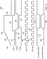
- FIG. 8 is a timing diagram 800 showing various waveforms related to a dual supply gate driver in accordance with some examples.
- the timing diagram 800 includes a bias input waveform 802, a bias_ok waveform 812, a Tri-stateA waveform 842, a Tri-stateB waveform 832, a Switch_ON waveform 852, a Switch_gate waveform 862 (corresponding to the gate signal for M7 at node 522 in FIG. 5 , or node 620 in FIG. 6 ), a VIN average current waveform 872, and a bias average current waveform 882.
- the switches between the drivers used to provide the Switch_gate waveform 862 e.g., switching between first and second driver circuits 514 and 516 in FIG. 5 ; or switching between first and second driver circuits 614 and 616 in FIG. 6
- the Switch_gate signal would be slightly delayed relative to the Switch_ON signal.
- the value of the bias_ok signal goes high during an interval 814 when the bias input reaches a threshold 804 as represented by the waveforms 802 and 812.
- Tri-stateA goes high during an interval 834 when the bias_ok signal goes high as represented by the waveforms 812 and 832.
- Tri-stateB stays low during the interval 814 as represented by the waveforms 812 and 842.
- the average VIN current drops to zero for an interval 874 as represented by the waveforms 832 and 872.
- the average current increases for an interval 884 as represented by the waveforms 832 and 882.
- the Switch_ON waveform 852 shows transitions between a high value 854 and a low value 856, where these transitions are not affected by the other values represented for the timing diagram 800. As shown, the Switch_gate waveform 852 follows the pattern of the Switch_ON waveform 852.
- the BIAS current maximum is less than the VIN current maximum (e.g., lower by several mA).
- selective use of dual drivers is implemented to improve efficiency of providing a drive signal (e.g., a low-side drive signal).
- the improvement in efficiency is due to the BIAS current being lower than the VIN current, which can be leveraged to reduce overall power consumption in a dual supply gate driver circuit (e.g., the dual supply gate driver circuits 500 or 600 of FIGS. 5 and 6 ) instead of single supply gate driver circuit.
- the described driver topologies avoid an external capacitor for drive operations to reduce the size and cost of the dual supply gate driver circuits described herein.
- FIG. 9 is a schematic diagram showing a driver circuit 900 (an example of the first driver circuit 514 in FIG. 5 , the second driver circuit 516 in FIG. 5 , the first driver circuit 614 in FIG. 6 , or the second driver circuit 616 in FIG. 6 ).
- the driver circuit 900 comprises a plurality of inverter circuits 903, 905, 907, and 909 in series between an input node 902 and an output node 916. More specifically, the first inverter circuit 903 includes two transistors, M8 and M9, coupled between a first input supply node 906 and a ground node 908.
- the first current terminal of M8 is coupled to the first input supply node 906 (e.g., to receive an input voltage of 1x, where x is a reference voltage level), the second current terminal of M8 is coupled to the first current terminal of M9, and the second current terminal of M9 is coupled to the ground node 908. Meanwhile, the control terminals for M8 and M9 are coupled to the input node 902.
- the second inverter circuit 905 includes two transistors, M10 and M11, coupled between a second input supply node 910 and the ground node 908. More specifically, the first current terminal of M10 is coupled to the second input supply node 910 (e.g., to receive an input voltage of nx, where n is an integer value greater than 1, and where x is a reference voltage level), the second current terminal of M10 is coupled to the first current terminal of M11, and the second current terminal of M11 is coupled to the ground node 908. Meanwhile, the control terminals for M10 and M11 are coupled to the output node 918 of the first inverter circuit 903.
- the third inverter circuit 907 includes two transistors, M12 and M13, coupled between a third input supply node 912 and the ground node 908. More specifically, the first current terminal of M12 is coupled to the third input supply node 912 (e.g., to receive an input voltage of n 2 x, where n is an integer value greater than 1, and where x is a reference voltage level), the second current terminal of M12 is coupled to the first current terminal of M13, and the second current terminal of M13 is coupled to the ground node 908. Meanwhile, the control terminals for M12 and M13 are coupled to the output node 920 of the second inverter circuit 905.
- the fourth inverter circuit 909 includes two transistors, M14 and M15, coupled between a fourth input supply node 914 and the ground node 908. More specifically, the first current terminal of M14 is coupled to the fourth input supply node 914 (e.g., to receive an input voltage of n 3 x, where n is an integer value greater than 1, and where x is a reference voltage level), the second current terminal of M14 is coupled to the first current terminal of M15, and the second current terminal of M15 is coupled to the ground node 908. Meanwhile, the control terminals for M14 and M15 are coupled to the output node 922 of the second inverter circuit 905. As shown, the output node 924 for the fourth inverter circuit 909 is coupled to the output node 916 for the driver circuit 916.
- Couple means either an indirect or direct wired or wireless connection.
- that connection may be through a direct connection or through an indirect connection via other devices and connections.
- the recitation "based on” means “based at least in part on.” Therefore, if X is based on Y, X may be a function of Y and any number of other factors.
Landscapes
- Engineering & Computer Science (AREA)
- Power Engineering (AREA)
- Physics & Mathematics (AREA)
- Electromagnetism (AREA)
- General Physics & Mathematics (AREA)
- Radar, Positioning & Navigation (AREA)
- Automation & Control Theory (AREA)
- Dc-Dc Converters (AREA)
- Continuous-Control Power Sources That Use Transistors (AREA)
- Power Conversion In General (AREA)
Applications Claiming Priority (3)
| Application Number | Priority Date | Filing Date | Title |
|---|---|---|---|
| US201862754926P | 2018-11-02 | 2018-11-02 | |
| US16/418,613 US10797579B2 (en) | 2018-11-02 | 2019-05-21 | Dual supply low-side gate driver |
| PCT/US2019/059316 WO2020092864A1 (en) | 2018-11-02 | 2019-11-01 | Dual supply low-side gate driver |
Publications (3)
| Publication Number | Publication Date |
|---|---|
| EP3874590A1 EP3874590A1 (en) | 2021-09-08 |
| EP3874590A4 EP3874590A4 (en) | 2022-01-05 |
| EP3874590B1 true EP3874590B1 (en) | 2024-01-24 |
Family
ID=70459266
Family Applications (1)
| Application Number | Title | Priority Date | Filing Date |
|---|---|---|---|
| EP19879052.9A Active EP3874590B1 (en) | 2018-11-02 | 2019-11-01 | Dual supply low-side gate driver |
Country Status (5)
| Country | Link |
|---|---|
| US (2) | US10797579B2 (https=) |
| EP (1) | EP3874590B1 (https=) |
| JP (1) | JP7408652B2 (https=) |
| CN (1) | CN112889210B (https=) |
| WO (1) | WO2020092864A1 (https=) |
Families Citing this family (7)
| Publication number | Priority date | Publication date | Assignee | Title |
|---|---|---|---|---|
| US10797579B2 (en) * | 2018-11-02 | 2020-10-06 | Texas Instruments Incorporated | Dual supply low-side gate driver |
| US11556144B2 (en) * | 2020-12-16 | 2023-01-17 | Skyworks Solutions, Inc. | High-speed low-impedance boosting low-dropout regulator |
| US11942860B2 (en) | 2021-05-26 | 2024-03-26 | Murata Manufacturing Co., Ltd. | Dynamic division ratio charge pump switching |
| CN113394973B (zh) * | 2021-06-07 | 2025-06-10 | 无锡芯朋微电子股份有限公司 | 一种电压转换电路以及一种非隔离电源系统 |
| US12122251B2 (en) | 2022-09-28 | 2024-10-22 | BorgWarner US Technologies LLC | Systems and methods for bidirectional message architecture for inverter for electric vehicle |
| US11936371B1 (en) | 2022-10-04 | 2024-03-19 | Psemi Corporation | Accurate reduced gate-drive current limiter |
| US12184174B2 (en) * | 2022-10-05 | 2024-12-31 | Murata Manufacturing Co., Ltd. | Reduced gate drive for power converter with dynamically switching ratio |
Family Cites Families (34)
| Publication number | Priority date | Publication date | Assignee | Title |
|---|---|---|---|---|
| JPS58105611U (ja) * | 1981-12-29 | 1983-07-18 | サンケン電気株式会社 | トランジスタ電圧レギユレ−タ |
| US5166538A (en) | 1986-12-15 | 1992-11-24 | Peter Norton | Dual or single voltage vehicular power supply with improved switch driver and load dump |
| DE4403309A1 (de) | 1994-02-03 | 1995-08-10 | Bayerische Motoren Werke Ag | Steuergerät mit einem ersten und zweiten elektrischen Versorgungseingang |
| US5940287A (en) * | 1998-07-14 | 1999-08-17 | Lucent Technologies Inc. | Controller for a synchronous rectifier and power converter employing the same |
| US6249111B1 (en) | 2000-06-22 | 2001-06-19 | Intel Corporation | Dual drive buck regulator |
| US6388506B1 (en) * | 2000-12-15 | 2002-05-14 | Marvell International, Ltd. | Regulator with leakage compensation |
| EP1361664B1 (en) * | 2002-05-10 | 2008-08-06 | Texas Instruments Incorporated | LDO regulator with sleep mode |
| JP4081604B2 (ja) | 2002-06-26 | 2008-04-30 | 株式会社豊田自動織機 | スイッチング素子の駆動装置 |
| US6940262B2 (en) * | 2002-12-31 | 2005-09-06 | Intersil Americas Inc. | PWM-based DC-DC converter with assured dead time control exhibiting no shoot-through current and independent of type of FET used |
| US7064529B2 (en) | 2003-09-17 | 2006-06-20 | Atmel Corporation | Dual stage voltage regulation circuit |
| EP1632827B1 (en) * | 2004-08-27 | 2007-05-23 | Infineon Technologies AG | Control circuit for current mode buck converter |
| US7345463B2 (en) * | 2006-07-07 | 2008-03-18 | Intersil Americas Inc. | Load compensated switching regulator |
| US7646115B2 (en) * | 2007-01-05 | 2010-01-12 | Standard Microsystems Corporation | Regulator circuit with multiple supply voltages |
| JP5112208B2 (ja) * | 2008-07-18 | 2013-01-09 | ルネサスエレクトロニクス株式会社 | レギュレータ及び半導体装置 |
| CN101686046B (zh) * | 2008-09-28 | 2013-12-18 | 飞思卡尔半导体公司 | H桥电路的新栅极驱动方法 |
| US8253399B2 (en) * | 2008-11-18 | 2012-08-28 | Texas Instruments Incorporated | Reconfigurable regulator and associated method |
| DE102008055051B4 (de) * | 2008-12-19 | 2014-05-08 | Infineon Technologies Austria Ag | Schaltungsanordnung und Verfahren zur Erzeugung eines Ansteuersignals für einen Transistor |
| JP2012527178A (ja) * | 2009-05-11 | 2012-11-01 | エスエス エスシー アイピー、エルエルシー | エンハンスメントモード型およびデプレションモード型のワイドバンドギャップ半導体jfetのためのゲートドライバ |
| US9793889B2 (en) * | 2011-03-15 | 2017-10-17 | Infineon Technologies Ag | Semiconductor device including a circuit to compensate for parasitic inductance |
| US8513937B2 (en) * | 2011-09-09 | 2013-08-20 | Micrel, Inc. | Switching regulator with optimized switch node rise time |
| JP2013062935A (ja) * | 2011-09-13 | 2013-04-04 | Toshiba Corp | 短絡保護回路およびdc−dcコンバータ |
| JP5840975B2 (ja) | 2012-02-22 | 2016-01-06 | 三菱電機株式会社 | ゲート駆動回路 |
| US9154026B2 (en) * | 2012-06-27 | 2015-10-06 | Intel Corporation | Bridge driver for a switching voltage regulator which is operable to soft-switch and hard-switch |
| JP6007804B2 (ja) * | 2013-01-28 | 2016-10-12 | 株式会社ソシオネクスト | 電源の制御回路、電源装置、電子機器及び電源の制御方法 |
| US8970265B2 (en) * | 2013-03-14 | 2015-03-03 | Allegro Microsystems, Llc | Systems and methods for driving a load under various power conditions |
| US9871444B2 (en) * | 2014-12-24 | 2018-01-16 | Texas Instruments Incorporated | Integrated circuit with configurable control and power switches |
| US9793890B2 (en) * | 2015-05-07 | 2017-10-17 | Infineon Technologies Austria Ag | System and method for a switch transistor driver |
| KR102365143B1 (ko) * | 2015-09-22 | 2022-02-18 | 삼성전자주식회사 | 멀티-파워와 게인-부스팅 기술을 이용하는 전압 레귤레이터와 이를 포함하는 모바일 장치들 |
| CN105553246B (zh) * | 2015-12-17 | 2018-06-05 | 华为技术有限公司 | 上下电驱动电路及其控制方法 |
| US10243443B2 (en) * | 2016-03-16 | 2019-03-26 | Analog Devices, Inc. | Bias voltage generator for n-channel based linear regulator |
| US9853637B1 (en) * | 2016-06-24 | 2017-12-26 | Infineon Technologies Ag | Dual gate switch device |
| US10594315B2 (en) * | 2017-02-01 | 2020-03-17 | Texas Instruments Incorporated | Switching rate monitoring and control |
| JP6992498B2 (ja) * | 2017-12-26 | 2022-01-13 | 株式会社デンソー | 駆動対象スイッチの駆動回路 |
| US10797579B2 (en) * | 2018-11-02 | 2020-10-06 | Texas Instruments Incorporated | Dual supply low-side gate driver |
-
2019
- 2019-05-21 US US16/418,613 patent/US10797579B2/en active Active
- 2019-11-01 WO PCT/US2019/059316 patent/WO2020092864A1/en not_active Ceased
- 2019-11-01 EP EP19879052.9A patent/EP3874590B1/en active Active
- 2019-11-01 JP JP2021524027A patent/JP7408652B2/ja active Active
- 2019-11-01 CN CN201980067562.9A patent/CN112889210B/zh active Active
-
2020
- 2020-09-03 US US17/011,184 patent/US11532979B2/en active Active
Also Published As
| Publication number | Publication date |
|---|---|
| US20200144925A1 (en) | 2020-05-07 |
| JP2022515313A (ja) | 2022-02-18 |
| EP3874590A4 (en) | 2022-01-05 |
| JP7408652B2 (ja) | 2024-01-05 |
| US11532979B2 (en) | 2022-12-20 |
| CN112889210B (zh) | 2024-06-28 |
| WO2020092864A1 (en) | 2020-05-07 |
| CN112889210A (zh) | 2021-06-01 |
| EP3874590A1 (en) | 2021-09-08 |
| US10797579B2 (en) | 2020-10-06 |
| US20200403491A1 (en) | 2020-12-24 |
Similar Documents
| Publication | Publication Date | Title |
|---|---|---|
| EP3874590B1 (en) | Dual supply low-side gate driver | |
| US10637456B2 (en) | Low voltage drop cascaded synchronous bootstrap supply circuit | |
| US8102157B2 (en) | Multi-output power supply device having charge pump circuit | |
| EP2973971B1 (en) | Systems and methods for 100 percent duty cycle in switching regulators | |
| US10256727B2 (en) | Multi-phase power supply with DC-DC converter integrated circuits having current sharing function | |
| JP4440869B2 (ja) | Dc−dcコンバータ、dc−dcコンバータの制御回路及びdc−dcコンバータの制御方法 | |
| US20200169160A1 (en) | Power supply control device and llc resonant converter | |
| US20200177087A1 (en) | Adjustable power supply device for supplying power to a power switch control device | |
| WO2016025514A1 (en) | Shared bootstrap capacitor for multiple phase buck converter circuit and methods | |
| WO2008111347A1 (en) | Switching regulator and method of controlling the same | |
| JP2017085725A (ja) | 降圧dc/dcコンバータおよびその制御回路、車載用電源装置 | |
| US20070262760A1 (en) | Multiple-output dc-dc converter | |
| US11750078B2 (en) | Adaptive off-time or on-time DC-DC converter | |
| US20170054368A1 (en) | Multi-Topology Power Converter Controller | |
| US20070120546A1 (en) | Compact voltage step-up/step-down switching regulator | |
| US11264898B2 (en) | Switching converter with multiple drive stages and related modes | |
| US8890498B2 (en) | Driving circuit to turn off switching element by voltage from voltage storage unit and converter including driving circuit | |
| US11637489B2 (en) | Isolated DC/DC converter and AC/DC converter | |
| US11532983B2 (en) | Systems and methods for reducing power loss of power converters | |
| EP2804303B1 (en) | Switching power supply circuit | |
| US11799386B2 (en) | Isolated power converter and data transmission method | |
| US20250175081A1 (en) | Enhancing efficiency of a switching converter | |
| US20260121541A1 (en) | Status report of power stage circuit for multiphase voltage regulator | |
| US20260121542A1 (en) | Pre-charge monitoring of power stage circuit for multiphase voltage regulator | |
| US20260012093A1 (en) | Circuit Device And Switching Regulator |
Legal Events
| Date | Code | Title | Description |
|---|---|---|---|
| STAA | Information on the status of an ep patent application or granted ep patent |
Free format text: STATUS: THE INTERNATIONAL PUBLICATION HAS BEEN MADE |
|
| PUAI | Public reference made under article 153(3) epc to a published international application that has entered the european phase |
Free format text: ORIGINAL CODE: 0009012 |
|
| STAA | Information on the status of an ep patent application or granted ep patent |
Free format text: STATUS: REQUEST FOR EXAMINATION WAS MADE |
|
| 17P | Request for examination filed |
Effective date: 20210602 |
|
| AK | Designated contracting states |
Kind code of ref document: A1 Designated state(s): AL AT BE BG CH CY CZ DE DK EE ES FI FR GB GR HR HU IE IS IT LI LT LU LV MC MK MT NL NO PL PT RO RS SE SI SK SM TR |
|
| A4 | Supplementary search report drawn up and despatched |
Effective date: 20211207 |
|
| RIC1 | Information provided on ipc code assigned before grant |
Ipc: B60R 16/03 20060101ALI20211201BHEP Ipc: H02M 3/156 20060101ALI20211201BHEP Ipc: H03K 17/0412 20060101ALI20211201BHEP Ipc: H03K 17/16 20060101AFI20211201BHEP |
|
| DAV | Request for validation of the european patent (deleted) | ||
| DAX | Request for extension of the european patent (deleted) | ||
| REG | Reference to a national code |
Ref country code: DE Ref legal event code: R079 Ipc: H03K0017160000 Ref document number: 602019045809 Country of ref document: DE Free format text: PREVIOUS MAIN CLASS: H02M0003156000 |
|
| GRAP | Despatch of communication of intention to grant a patent |
Free format text: ORIGINAL CODE: EPIDOSNIGR1 |
|
| STAA | Information on the status of an ep patent application or granted ep patent |
Free format text: STATUS: GRANT OF PATENT IS INTENDED |
|
| RIC1 | Information provided on ipc code assigned before grant |
Ipc: B60R 16/03 20060101ALI20230906BHEP Ipc: H02M 3/156 20060101ALI20230906BHEP Ipc: H03K 17/0412 20060101ALI20230906BHEP Ipc: H03K 17/16 20060101AFI20230906BHEP |
|
| INTG | Intention to grant announced |
Effective date: 20230919 |
|
| RAP3 | Party data changed (applicant data changed or rights of an application transferred) |
Owner name: TEXAS INSTRUMENTS INCORPORATED |
|
| GRAS | Grant fee paid |
Free format text: ORIGINAL CODE: EPIDOSNIGR3 |
|
| GRAA | (expected) grant |
Free format text: ORIGINAL CODE: 0009210 |
|
| STAA | Information on the status of an ep patent application or granted ep patent |
Free format text: STATUS: THE PATENT HAS BEEN GRANTED |
|
| P01 | Opt-out of the competence of the unified patent court (upc) registered |
Effective date: 20231122 |
|
| AK | Designated contracting states |
Kind code of ref document: B1 Designated state(s): AL AT BE BG CH CY CZ DE DK EE ES FI FR GB GR HR HU IE IS IT LI LT LU LV MC MK MT NL NO PL PT RO RS SE SI SK SM TR |
|
| REG | Reference to a national code |
Ref country code: GB Ref legal event code: FG4D |
|
| REG | Reference to a national code |
Ref country code: CH Ref legal event code: EP |
|
| REG | Reference to a national code |
Ref country code: DE Ref legal event code: R096 Ref document number: 602019045809 Country of ref document: DE |
|
| REG | Reference to a national code |
Ref country code: IE Ref legal event code: FG4D |
|
| REG | Reference to a national code |
Ref country code: LT Ref legal event code: MG9D |
|
| REG | Reference to a national code |
Ref country code: NL Ref legal event code: MP Effective date: 20240124 |
|
| PG25 | Lapsed in a contracting state [announced via postgrant information from national office to epo] |
Ref country code: NL Free format text: LAPSE BECAUSE OF FAILURE TO SUBMIT A TRANSLATION OF THE DESCRIPTION OR TO PAY THE FEE WITHIN THE PRESCRIBED TIME-LIMIT Effective date: 20240124 |
|
| PG25 | Lapsed in a contracting state [announced via postgrant information from national office to epo] |
Ref country code: NL Free format text: LAPSE BECAUSE OF FAILURE TO SUBMIT A TRANSLATION OF THE DESCRIPTION OR TO PAY THE FEE WITHIN THE PRESCRIBED TIME-LIMIT Effective date: 20240124 |
|
| PG25 | Lapsed in a contracting state [announced via postgrant information from national office to epo] |
Ref country code: IS Free format text: LAPSE BECAUSE OF FAILURE TO SUBMIT A TRANSLATION OF THE DESCRIPTION OR TO PAY THE FEE WITHIN THE PRESCRIBED TIME-LIMIT Effective date: 20240524 |
|
| PG25 | Lapsed in a contracting state [announced via postgrant information from national office to epo] |
Ref country code: LT Free format text: LAPSE BECAUSE OF FAILURE TO SUBMIT A TRANSLATION OF THE DESCRIPTION OR TO PAY THE FEE WITHIN THE PRESCRIBED TIME-LIMIT Effective date: 20240124 |
|
| PG25 | Lapsed in a contracting state [announced via postgrant information from national office to epo] |
Ref country code: GR Free format text: LAPSE BECAUSE OF FAILURE TO SUBMIT A TRANSLATION OF THE DESCRIPTION OR TO PAY THE FEE WITHIN THE PRESCRIBED TIME-LIMIT Effective date: 20240425 |
|
| REG | Reference to a national code |
Ref country code: AT Ref legal event code: MK05 Ref document number: 1652973 Country of ref document: AT Kind code of ref document: T Effective date: 20240124 |
|
| PG25 | Lapsed in a contracting state [announced via postgrant information from national office to epo] |
Ref country code: HR Free format text: LAPSE BECAUSE OF FAILURE TO SUBMIT A TRANSLATION OF THE DESCRIPTION OR TO PAY THE FEE WITHIN THE PRESCRIBED TIME-LIMIT Effective date: 20240124 Ref country code: RS Free format text: LAPSE BECAUSE OF FAILURE TO SUBMIT A TRANSLATION OF THE DESCRIPTION OR TO PAY THE FEE WITHIN THE PRESCRIBED TIME-LIMIT Effective date: 20240424 |
|
| PG25 | Lapsed in a contracting state [announced via postgrant information from national office to epo] |
Ref country code: ES Free format text: LAPSE BECAUSE OF FAILURE TO SUBMIT A TRANSLATION OF THE DESCRIPTION OR TO PAY THE FEE WITHIN THE PRESCRIBED TIME-LIMIT Effective date: 20240124 |
|
| PG25 | Lapsed in a contracting state [announced via postgrant information from national office to epo] |
Ref country code: AT Free format text: LAPSE BECAUSE OF FAILURE TO SUBMIT A TRANSLATION OF THE DESCRIPTION OR TO PAY THE FEE WITHIN THE PRESCRIBED TIME-LIMIT Effective date: 20240124 |
|
| PG25 | Lapsed in a contracting state [announced via postgrant information from national office to epo] |
Ref country code: RS Free format text: LAPSE BECAUSE OF FAILURE TO SUBMIT A TRANSLATION OF THE DESCRIPTION OR TO PAY THE FEE WITHIN THE PRESCRIBED TIME-LIMIT Effective date: 20240424 Ref country code: NO Free format text: LAPSE BECAUSE OF FAILURE TO SUBMIT A TRANSLATION OF THE DESCRIPTION OR TO PAY THE FEE WITHIN THE PRESCRIBED TIME-LIMIT Effective date: 20240424 Ref country code: LT Free format text: LAPSE BECAUSE OF FAILURE TO SUBMIT A TRANSLATION OF THE DESCRIPTION OR TO PAY THE FEE WITHIN THE PRESCRIBED TIME-LIMIT Effective date: 20240124 Ref country code: IS Free format text: LAPSE BECAUSE OF FAILURE TO SUBMIT A TRANSLATION OF THE DESCRIPTION OR TO PAY THE FEE WITHIN THE PRESCRIBED TIME-LIMIT Effective date: 20240524 Ref country code: HR Free format text: LAPSE BECAUSE OF FAILURE TO SUBMIT A TRANSLATION OF THE DESCRIPTION OR TO PAY THE FEE WITHIN THE PRESCRIBED TIME-LIMIT Effective date: 20240124 Ref country code: GR Free format text: LAPSE BECAUSE OF FAILURE TO SUBMIT A TRANSLATION OF THE DESCRIPTION OR TO PAY THE FEE WITHIN THE PRESCRIBED TIME-LIMIT Effective date: 20240425 Ref country code: FI Free format text: LAPSE BECAUSE OF FAILURE TO SUBMIT A TRANSLATION OF THE DESCRIPTION OR TO PAY THE FEE WITHIN THE PRESCRIBED TIME-LIMIT Effective date: 20240124 Ref country code: ES Free format text: LAPSE BECAUSE OF FAILURE TO SUBMIT A TRANSLATION OF THE DESCRIPTION OR TO PAY THE FEE WITHIN THE PRESCRIBED TIME-LIMIT Effective date: 20240124 Ref country code: BG Free format text: LAPSE BECAUSE OF FAILURE TO SUBMIT A TRANSLATION OF THE DESCRIPTION OR TO PAY THE FEE WITHIN THE PRESCRIBED TIME-LIMIT Effective date: 20240124 Ref country code: AT Free format text: LAPSE BECAUSE OF FAILURE TO SUBMIT A TRANSLATION OF THE DESCRIPTION OR TO PAY THE FEE WITHIN THE PRESCRIBED TIME-LIMIT Effective date: 20240124 |
|
| PG25 | Lapsed in a contracting state [announced via postgrant information from national office to epo] |
Ref country code: PL Free format text: LAPSE BECAUSE OF FAILURE TO SUBMIT A TRANSLATION OF THE DESCRIPTION OR TO PAY THE FEE WITHIN THE PRESCRIBED TIME-LIMIT Effective date: 20240124 Ref country code: PT Free format text: LAPSE BECAUSE OF FAILURE TO SUBMIT A TRANSLATION OF THE DESCRIPTION OR TO PAY THE FEE WITHIN THE PRESCRIBED TIME-LIMIT Effective date: 20240524 |
|
| PG25 | Lapsed in a contracting state [announced via postgrant information from national office to epo] |
Ref country code: SE Free format text: LAPSE BECAUSE OF FAILURE TO SUBMIT A TRANSLATION OF THE DESCRIPTION OR TO PAY THE FEE WITHIN THE PRESCRIBED TIME-LIMIT Effective date: 20240124 Ref country code: PT Free format text: LAPSE BECAUSE OF FAILURE TO SUBMIT A TRANSLATION OF THE DESCRIPTION OR TO PAY THE FEE WITHIN THE PRESCRIBED TIME-LIMIT Effective date: 20240524 Ref country code: PL Free format text: LAPSE BECAUSE OF FAILURE TO SUBMIT A TRANSLATION OF THE DESCRIPTION OR TO PAY THE FEE WITHIN THE PRESCRIBED TIME-LIMIT Effective date: 20240124 Ref country code: LV Free format text: LAPSE BECAUSE OF FAILURE TO SUBMIT A TRANSLATION OF THE DESCRIPTION OR TO PAY THE FEE WITHIN THE PRESCRIBED TIME-LIMIT Effective date: 20240124 |
|
| PG25 | Lapsed in a contracting state [announced via postgrant information from national office to epo] |
Ref country code: DK Free format text: LAPSE BECAUSE OF FAILURE TO SUBMIT A TRANSLATION OF THE DESCRIPTION OR TO PAY THE FEE WITHIN THE PRESCRIBED TIME-LIMIT Effective date: 20240124 |
|
| PG25 | Lapsed in a contracting state [announced via postgrant information from national office to epo] |
Ref country code: SM Free format text: LAPSE BECAUSE OF FAILURE TO SUBMIT A TRANSLATION OF THE DESCRIPTION OR TO PAY THE FEE WITHIN THE PRESCRIBED TIME-LIMIT Effective date: 20240124 |
|
| PG25 | Lapsed in a contracting state [announced via postgrant information from national office to epo] |
Ref country code: CZ Free format text: LAPSE BECAUSE OF FAILURE TO SUBMIT A TRANSLATION OF THE DESCRIPTION OR TO PAY THE FEE WITHIN THE PRESCRIBED TIME-LIMIT Effective date: 20240124 Ref country code: EE Free format text: LAPSE BECAUSE OF FAILURE TO SUBMIT A TRANSLATION OF THE DESCRIPTION OR TO PAY THE FEE WITHIN THE PRESCRIBED TIME-LIMIT Effective date: 20240124 |
|
| REG | Reference to a national code |
Ref country code: DE Ref legal event code: R097 Ref document number: 602019045809 Country of ref document: DE |
|
| PG25 | Lapsed in a contracting state [announced via postgrant information from national office to epo] |
Ref country code: SK Free format text: LAPSE BECAUSE OF FAILURE TO SUBMIT A TRANSLATION OF THE DESCRIPTION OR TO PAY THE FEE WITHIN THE PRESCRIBED TIME-LIMIT Effective date: 20240124 |
|
| PG25 | Lapsed in a contracting state [announced via postgrant information from national office to epo] |
Ref country code: SM Free format text: LAPSE BECAUSE OF FAILURE TO SUBMIT A TRANSLATION OF THE DESCRIPTION OR TO PAY THE FEE WITHIN THE PRESCRIBED TIME-LIMIT Effective date: 20240124 Ref country code: SK Free format text: LAPSE BECAUSE OF FAILURE TO SUBMIT A TRANSLATION OF THE DESCRIPTION OR TO PAY THE FEE WITHIN THE PRESCRIBED TIME-LIMIT Effective date: 20240124 Ref country code: EE Free format text: LAPSE BECAUSE OF FAILURE TO SUBMIT A TRANSLATION OF THE DESCRIPTION OR TO PAY THE FEE WITHIN THE PRESCRIBED TIME-LIMIT Effective date: 20240124 Ref country code: DK Free format text: LAPSE BECAUSE OF FAILURE TO SUBMIT A TRANSLATION OF THE DESCRIPTION OR TO PAY THE FEE WITHIN THE PRESCRIBED TIME-LIMIT Effective date: 20240124 Ref country code: CZ Free format text: LAPSE BECAUSE OF FAILURE TO SUBMIT A TRANSLATION OF THE DESCRIPTION OR TO PAY THE FEE WITHIN THE PRESCRIBED TIME-LIMIT Effective date: 20240124 |
|
| PLBE | No opposition filed within time limit |
Free format text: ORIGINAL CODE: 0009261 |
|
| STAA | Information on the status of an ep patent application or granted ep patent |
Free format text: STATUS: NO OPPOSITION FILED WITHIN TIME LIMIT |
|
| PG25 | Lapsed in a contracting state [announced via postgrant information from national office to epo] |
Ref country code: IT Free format text: LAPSE BECAUSE OF FAILURE TO SUBMIT A TRANSLATION OF THE DESCRIPTION OR TO PAY THE FEE WITHIN THE PRESCRIBED TIME-LIMIT Effective date: 20240124 |
|
| PG25 | Lapsed in a contracting state [announced via postgrant information from national office to epo] |
Ref country code: IT Free format text: LAPSE BECAUSE OF FAILURE TO SUBMIT A TRANSLATION OF THE DESCRIPTION OR TO PAY THE FEE WITHIN THE PRESCRIBED TIME-LIMIT Effective date: 20240124 |
|
| 26N | No opposition filed |
Effective date: 20241025 |
|
| PG25 | Lapsed in a contracting state [announced via postgrant information from national office to epo] |
Ref country code: SI Free format text: LAPSE BECAUSE OF FAILURE TO SUBMIT A TRANSLATION OF THE DESCRIPTION OR TO PAY THE FEE WITHIN THE PRESCRIBED TIME-LIMIT Effective date: 20240124 |
|
| REG | Reference to a national code |
Ref country code: CH Ref legal event code: PL |
|
| PG25 | Lapsed in a contracting state [announced via postgrant information from national office to epo] |
Ref country code: MC Free format text: LAPSE BECAUSE OF FAILURE TO SUBMIT A TRANSLATION OF THE DESCRIPTION OR TO PAY THE FEE WITHIN THE PRESCRIBED TIME-LIMIT Effective date: 20240124 |
|
| PG25 | Lapsed in a contracting state [announced via postgrant information from national office to epo] |
Ref country code: LU Free format text: LAPSE BECAUSE OF NON-PAYMENT OF DUE FEES Effective date: 20241101 |
|
| REG | Reference to a national code |
Ref country code: CH Ref legal event code: PL |
|
| PG25 | Lapsed in a contracting state [announced via postgrant information from national office to epo] |
Ref country code: CH Free format text: LAPSE BECAUSE OF NON-PAYMENT OF DUE FEES Effective date: 20241130 |
|
| REG | Reference to a national code |
Ref country code: BE Ref legal event code: MM Effective date: 20241130 |
|
| PG25 | Lapsed in a contracting state [announced via postgrant information from national office to epo] |
Ref country code: BE Free format text: LAPSE BECAUSE OF NON-PAYMENT OF DUE FEES Effective date: 20241130 |
|
| PG25 | Lapsed in a contracting state [announced via postgrant information from national office to epo] |
Ref country code: IE Free format text: LAPSE BECAUSE OF NON-PAYMENT OF DUE FEES Effective date: 20241101 |
|
| PG25 | Lapsed in a contracting state [announced via postgrant information from national office to epo] |
Ref country code: RO Free format text: LAPSE BECAUSE OF FAILURE TO SUBMIT A TRANSLATION OF THE DESCRIPTION OR TO PAY THE FEE WITHIN THE PRESCRIBED TIME-LIMIT Effective date: 20240124 |
|
| PGFP | Annual fee paid to national office [announced via postgrant information from national office to epo] |
Ref country code: DE Payment date: 20251022 Year of fee payment: 7 |
|
| PGFP | Annual fee paid to national office [announced via postgrant information from national office to epo] |
Ref country code: GB Payment date: 20251023 Year of fee payment: 7 |
|
| PGFP | Annual fee paid to national office [announced via postgrant information from national office to epo] |
Ref country code: FR Payment date: 20251022 Year of fee payment: 7 |
|
| PG25 | Lapsed in a contracting state [announced via postgrant information from national office to epo] |
Ref country code: HU Free format text: LAPSE BECAUSE OF FAILURE TO SUBMIT A TRANSLATION OF THE DESCRIPTION OR TO PAY THE FEE WITHIN THE PRESCRIBED TIME-LIMIT; INVALID AB INITIO Effective date: 20191101 |
|
| PG25 | Lapsed in a contracting state [announced via postgrant information from national office to epo] |
Ref country code: CY Free format text: LAPSE BECAUSE OF FAILURE TO SUBMIT A TRANSLATION OF THE DESCRIPTION OR TO PAY THE FEE WITHIN THE PRESCRIBED TIME-LIMIT; INVALID AB INITIO Effective date: 20191101 |