EP3846211B1 - System to operate x-ray detector having driver micro integrated chips printed on photodiode layer - Google Patents
System to operate x-ray detector having driver micro integrated chips printed on photodiode layer Download PDFInfo
- Publication number
- EP3846211B1 EP3846211B1 EP20166711.0A EP20166711A EP3846211B1 EP 3846211 B1 EP3846211 B1 EP 3846211B1 EP 20166711 A EP20166711 A EP 20166711A EP 3846211 B1 EP3846211 B1 EP 3846211B1
- Authority
- EP
- European Patent Office
- Prior art keywords
- layer
- pixel driving
- photodiode
- integrated chips
- ray detector
- Prior art date
- Legal status (The legal status is an assumption and is not a legal conclusion. Google has not performed a legal analysis and makes no representation as to the accuracy of the status listed.)
- Active
Links
Images


Classifications
-
- H—ELECTRICITY
- H10—SEMICONDUCTOR DEVICES; ELECTRIC SOLID-STATE DEVICES NOT OTHERWISE PROVIDED FOR
- H10F—INORGANIC SEMICONDUCTOR DEVICES SENSITIVE TO INFRARED RADIATION, LIGHT, ELECTROMAGNETIC RADIATION OF SHORTER WAVELENGTH OR CORPUSCULAR RADIATION
- H10F39/00—Integrated devices, or assemblies of multiple devices, comprising at least one element covered by group H10F30/00, e.g. radiation detectors comprising photodiode arrays
- H10F39/80—Constructional details of image sensors
- H10F39/802—Geometry or disposition of elements in pixels, e.g. address-lines or gate electrodes
-
- H—ELECTRICITY
- H10—SEMICONDUCTOR DEVICES; ELECTRIC SOLID-STATE DEVICES NOT OTHERWISE PROVIDED FOR
- H10F—INORGANIC SEMICONDUCTOR DEVICES SENSITIVE TO INFRARED RADIATION, LIGHT, ELECTROMAGNETIC RADIATION OF SHORTER WAVELENGTH OR CORPUSCULAR RADIATION
- H10F39/00—Integrated devices, or assemblies of multiple devices, comprising at least one element covered by group H10F30/00, e.g. radiation detectors comprising photodiode arrays
- H10F39/10—Integrated devices
- H10F39/12—Image sensors
- H10F39/18—Complementary metal-oxide-semiconductor [CMOS] image sensors; Photodiode array image sensors
- H10F39/189—X-ray, gamma-ray or corpuscular radiation imagers
-
- G—PHYSICS
- G01—MEASURING; TESTING
- G01T—MEASUREMENT OF NUCLEAR OR X-RADIATION
- G01T1/00—Measuring X-radiation, gamma radiation, corpuscular radiation, or cosmic radiation
- G01T1/16—Measuring radiation intensity
- G01T1/20—Measuring radiation intensity with scintillation detectors
- G01T1/208—Circuits specially adapted for scintillation detectors, e.g. for the photo-multiplier section
-
- B—PERFORMING OPERATIONS; TRANSPORTING
- B41—PRINTING; LINING MACHINES; TYPEWRITERS; STAMPS
- B41F—PRINTING MACHINES OR PRESSES
- B41F16/00—Transfer printing apparatus
-
- G—PHYSICS
- G01—MEASURING; TESTING
- G01T—MEASUREMENT OF NUCLEAR OR X-RADIATION
- G01T1/00—Measuring X-radiation, gamma radiation, corpuscular radiation, or cosmic radiation
- G01T1/16—Measuring radiation intensity
- G01T1/1603—Measuring radiation intensity with a combination of at least two different types of detector
-
- G—PHYSICS
- G01—MEASURING; TESTING
- G01T—MEASUREMENT OF NUCLEAR OR X-RADIATION
- G01T1/00—Measuring X-radiation, gamma radiation, corpuscular radiation, or cosmic radiation
- G01T1/16—Measuring radiation intensity
- G01T1/161—Applications in the field of nuclear medicine, e.g. in vivo counting
-
- G—PHYSICS
- G01—MEASURING; TESTING
- G01T—MEASUREMENT OF NUCLEAR OR X-RADIATION
- G01T1/00—Measuring X-radiation, gamma radiation, corpuscular radiation, or cosmic radiation
- G01T1/16—Measuring radiation intensity
- G01T1/20—Measuring radiation intensity with scintillation detectors
- G01T1/2008—Measuring radiation intensity with scintillation detectors using a combination of different types of scintillation detectors, e.g. phoswich
-
- G—PHYSICS
- G01—MEASURING; TESTING
- G01T—MEASUREMENT OF NUCLEAR OR X-RADIATION
- G01T1/00—Measuring X-radiation, gamma radiation, corpuscular radiation, or cosmic radiation
- G01T1/16—Measuring radiation intensity
- G01T1/20—Measuring radiation intensity with scintillation detectors
- G01T1/2018—Scintillation-photodiode combinations
-
- G—PHYSICS
- G01—MEASURING; TESTING
- G01T—MEASUREMENT OF NUCLEAR OR X-RADIATION
- G01T1/00—Measuring X-radiation, gamma radiation, corpuscular radiation, or cosmic radiation
- G01T1/16—Measuring radiation intensity
- G01T1/24—Measuring radiation intensity with semiconductor detectors
-
- G—PHYSICS
- G01—MEASURING; TESTING
- G01T—MEASUREMENT OF NUCLEAR OR X-RADIATION
- G01T1/00—Measuring X-radiation, gamma radiation, corpuscular radiation, or cosmic radiation
- G01T1/16—Measuring radiation intensity
- G01T1/24—Measuring radiation intensity with semiconductor detectors
- G01T1/241—Electrode arrangements, e.g. continuous or parallel strips or the like
-
- G—PHYSICS
- G01—MEASURING; TESTING
- G01T—MEASUREMENT OF NUCLEAR OR X-RADIATION
- G01T1/00—Measuring X-radiation, gamma radiation, corpuscular radiation, or cosmic radiation
- G01T1/16—Measuring radiation intensity
- G01T1/24—Measuring radiation intensity with semiconductor detectors
- G01T1/242—Stacked detectors, e.g. for depth information
-
- G—PHYSICS
- G01—MEASURING; TESTING
- G01T—MEASUREMENT OF NUCLEAR OR X-RADIATION
- G01T1/00—Measuring X-radiation, gamma radiation, corpuscular radiation, or cosmic radiation
- G01T1/16—Measuring radiation intensity
- G01T1/24—Measuring radiation intensity with semiconductor detectors
- G01T1/246—Measuring radiation intensity with semiconductor detectors utilizing latent read-out, e.g. charge stored and read-out later
-
- G—PHYSICS
- G01—MEASURING; TESTING
- G01T—MEASUREMENT OF NUCLEAR OR X-RADIATION
- G01T1/00—Measuring X-radiation, gamma radiation, corpuscular radiation, or cosmic radiation
- G01T1/16—Measuring radiation intensity
- G01T1/24—Measuring radiation intensity with semiconductor detectors
- G01T1/247—Detector read-out circuitry
-
- H—ELECTRICITY
- H10—SEMICONDUCTOR DEVICES; ELECTRIC SOLID-STATE DEVICES NOT OTHERWISE PROVIDED FOR
- H10F—INORGANIC SEMICONDUCTOR DEVICES SENSITIVE TO INFRARED RADIATION, LIGHT, ELECTROMAGNETIC RADIATION OF SHORTER WAVELENGTH OR CORPUSCULAR RADIATION
- H10F30/00—Individual radiation-sensitive semiconductor devices in which radiation controls the flow of current through the devices, e.g. photodetectors
- H10F30/20—Individual radiation-sensitive semiconductor devices in which radiation controls the flow of current through the devices, e.g. photodetectors the devices having potential barriers, e.g. phototransistors
- H10F30/29—Individual radiation-sensitive semiconductor devices in which radiation controls the flow of current through the devices, e.g. photodetectors the devices having potential barriers, e.g. phototransistors the devices being sensitive to radiation having very short wavelengths, e.g. X-rays, gamma-rays or corpuscular radiation
-
- H—ELECTRICITY
- H10—SEMICONDUCTOR DEVICES; ELECTRIC SOLID-STATE DEVICES NOT OTHERWISE PROVIDED FOR
- H10F—INORGANIC SEMICONDUCTOR DEVICES SENSITIVE TO INFRARED RADIATION, LIGHT, ELECTROMAGNETIC RADIATION OF SHORTER WAVELENGTH OR CORPUSCULAR RADIATION
- H10F39/00—Integrated devices, or assemblies of multiple devices, comprising at least one element covered by group H10F30/00, e.g. radiation detectors comprising photodiode arrays
- H10F39/011—Manufacture or treatment of image sensors covered by group H10F39/12
- H10F39/014—Manufacture or treatment of image sensors covered by group H10F39/12 of CMOS image sensors
-
- H—ELECTRICITY
- H10—SEMICONDUCTOR DEVICES; ELECTRIC SOLID-STATE DEVICES NOT OTHERWISE PROVIDED FOR
- H10F—INORGANIC SEMICONDUCTOR DEVICES SENSITIVE TO INFRARED RADIATION, LIGHT, ELECTROMAGNETIC RADIATION OF SHORTER WAVELENGTH OR CORPUSCULAR RADIATION
- H10F39/00—Integrated devices, or assemblies of multiple devices, comprising at least one element covered by group H10F30/00, e.g. radiation detectors comprising photodiode arrays
- H10F39/011—Manufacture or treatment of image sensors covered by group H10F39/12
- H10F39/018—Manufacture or treatment of image sensors covered by group H10F39/12 of hybrid image sensors
-
- H—ELECTRICITY
- H10—SEMICONDUCTOR DEVICES; ELECTRIC SOLID-STATE DEVICES NOT OTHERWISE PROVIDED FOR
- H10F—INORGANIC SEMICONDUCTOR DEVICES SENSITIVE TO INFRARED RADIATION, LIGHT, ELECTROMAGNETIC RADIATION OF SHORTER WAVELENGTH OR CORPUSCULAR RADIATION
- H10F39/00—Integrated devices, or assemblies of multiple devices, comprising at least one element covered by group H10F30/00, e.g. radiation detectors comprising photodiode arrays
- H10F39/011—Manufacture or treatment of image sensors covered by group H10F39/12
- H10F39/026—Wafer-level processing
-
- H—ELECTRICITY
- H10—SEMICONDUCTOR DEVICES; ELECTRIC SOLID-STATE DEVICES NOT OTHERWISE PROVIDED FOR
- H10F—INORGANIC SEMICONDUCTOR DEVICES SENSITIVE TO INFRARED RADIATION, LIGHT, ELECTROMAGNETIC RADIATION OF SHORTER WAVELENGTH OR CORPUSCULAR RADIATION
- H10F39/00—Integrated devices, or assemblies of multiple devices, comprising at least one element covered by group H10F30/00, e.g. radiation detectors comprising photodiode arrays
- H10F39/10—Integrated devices
- H10F39/12—Image sensors
- H10F39/18—Complementary metal-oxide-semiconductor [CMOS] image sensors; Photodiode array image sensors
- H10F39/189—X-ray, gamma-ray or corpuscular radiation imagers
- H10F39/1895—X-ray, gamma-ray or corpuscular radiation imagers of the hybrid type
-
- H—ELECTRICITY
- H10—SEMICONDUCTOR DEVICES; ELECTRIC SOLID-STATE DEVICES NOT OTHERWISE PROVIDED FOR
- H10F—INORGANIC SEMICONDUCTOR DEVICES SENSITIVE TO INFRARED RADIATION, LIGHT, ELECTROMAGNETIC RADIATION OF SHORTER WAVELENGTH OR CORPUSCULAR RADIATION
- H10F39/00—Integrated devices, or assemblies of multiple devices, comprising at least one element covered by group H10F30/00, e.g. radiation detectors comprising photodiode arrays
- H10F39/10—Integrated devices
- H10F39/12—Image sensors
- H10F39/18—Complementary metal-oxide-semiconductor [CMOS] image sensors; Photodiode array image sensors
- H10F39/189—X-ray, gamma-ray or corpuscular radiation imagers
- H10F39/1898—Indirect radiation image sensors, e.g. using luminescent members
-
- H—ELECTRICITY
- H10—SEMICONDUCTOR DEVICES; ELECTRIC SOLID-STATE DEVICES NOT OTHERWISE PROVIDED FOR
- H10F—INORGANIC SEMICONDUCTOR DEVICES SENSITIVE TO INFRARED RADIATION, LIGHT, ELECTROMAGNETIC RADIATION OF SHORTER WAVELENGTH OR CORPUSCULAR RADIATION
- H10F39/00—Integrated devices, or assemblies of multiple devices, comprising at least one element covered by group H10F30/00, e.g. radiation detectors comprising photodiode arrays
- H10F39/80—Constructional details of image sensors
- H10F39/809—Constructional details of image sensors of hybrid image sensors
-
- H—ELECTRICITY
- H10—SEMICONDUCTOR DEVICES; ELECTRIC SOLID-STATE DEVICES NOT OTHERWISE PROVIDED FOR
- H10F—INORGANIC SEMICONDUCTOR DEVICES SENSITIVE TO INFRARED RADIATION, LIGHT, ELECTROMAGNETIC RADIATION OF SHORTER WAVELENGTH OR CORPUSCULAR RADIATION
- H10F39/00—Integrated devices, or assemblies of multiple devices, comprising at least one element covered by group H10F30/00, e.g. radiation detectors comprising photodiode arrays
- H10F39/80—Constructional details of image sensors
- H10F39/811—Interconnections
-
- H—ELECTRICITY
- H10—SEMICONDUCTOR DEVICES; ELECTRIC SOLID-STATE DEVICES NOT OTHERWISE PROVIDED FOR
- H10F—INORGANIC SEMICONDUCTOR DEVICES SENSITIVE TO INFRARED RADIATION, LIGHT, ELECTROMAGNETIC RADIATION OF SHORTER WAVELENGTH OR CORPUSCULAR RADIATION
- H10F71/00—Manufacture or treatment of devices covered by this subclass
- H10F71/137—Batch treatment of the devices
-
- H—ELECTRICITY
- H10—SEMICONDUCTOR DEVICES; ELECTRIC SOLID-STATE DEVICES NOT OTHERWISE PROVIDED FOR
- H10F—INORGANIC SEMICONDUCTOR DEVICES SENSITIVE TO INFRARED RADIATION, LIGHT, ELECTROMAGNETIC RADIATION OF SHORTER WAVELENGTH OR CORPUSCULAR RADIATION
- H10F71/00—Manufacture or treatment of devices covered by this subclass
- H10F71/139—Manufacture or treatment of devices covered by this subclass using temporary substrates
-
- H—ELECTRICITY
- H10—SEMICONDUCTOR DEVICES; ELECTRIC SOLID-STATE DEVICES NOT OTHERWISE PROVIDED FOR
- H10F—INORGANIC SEMICONDUCTOR DEVICES SENSITIVE TO INFRARED RADIATION, LIGHT, ELECTROMAGNETIC RADIATION OF SHORTER WAVELENGTH OR CORPUSCULAR RADIATION
- H10F77/00—Constructional details of devices covered by this subclass
- H10F77/10—Semiconductor bodies
- H10F77/16—Material structures, e.g. crystalline structures, film structures or crystal plane orientations
- H10F77/162—Non-monocrystalline materials, e.g. semiconductor particles embedded in insulating materials
- H10F77/164—Polycrystalline semiconductors
-
- H—ELECTRICITY
- H10—SEMICONDUCTOR DEVICES; ELECTRIC SOLID-STATE DEVICES NOT OTHERWISE PROVIDED FOR
- H10F—INORGANIC SEMICONDUCTOR DEVICES SENSITIVE TO INFRARED RADIATION, LIGHT, ELECTROMAGNETIC RADIATION OF SHORTER WAVELENGTH OR CORPUSCULAR RADIATION
- H10F77/00—Constructional details of devices covered by this subclass
- H10F77/10—Semiconductor bodies
- H10F77/16—Material structures, e.g. crystalline structures, film structures or crystal plane orientations
- H10F77/162—Non-monocrystalline materials, e.g. semiconductor particles embedded in insulating materials
- H10F77/166—Amorphous semiconductors
Definitions
- the present disclosure relates to an X-ray detector. More particularly, the present disclosure relates to an X-ray detector including a plurality of pixel driving micro integrated chips (in the following also referred to as pixel driving integrated chips) printed on a plurality of photodiodes and each of the pixel driving integrated chips sequentially controlling multiple pixels.
- pixel driving micro integrated chips in the following also referred to as pixel driving integrated chips
- a digital X-ray detector In medical or industrial radiography, a digital X-ray detector has been widely used. Such a digital X-ray detector may be commonly referred to as an X-ray detector or an image detector. Further, such a digital detector may be classified into an indirect conversion type X-ray detector and a direct conversion type X-ray detector.
- the indirect conversion type X-ray detector i) converts X-rays (e.g., X-ray photons) into visible light (e.g., light photons) using a scintillator and ii) converts the visible light into an electric signal.
- the direct conversion digital detector directly converts X-rays into an electric signal using a photoconductive layer.
- an X-ray detector detects X-ray signals that are radiated from an X-ray source, have passed through a target object, and reached to the X-ray detector.
- the X-ray detector converts the detected X-ray signals into electric signals.
- Such an X-ray detector includes a pixel array panel including a plurality of pixels. Each pixel includes a light receiving element (e.g., photoconductor or photodiode) and a driving element for driving the light receiving element of each pixel.
- Such an X-ray detector may be manufactured using a thin-film transistor (TFT) process or a complementary metal-oxide-semiconductor (CMOS) process.
- TFT thin-film transistor
- CMOS complementary metal-oxide-semiconductor
- the TFT process is advantageous for manufacturing a large surface X-ray detector with a low manufacture unit price.
- the CMOS process is advantageous for manufacturing a high image quality X-ray detector generating comparably low radiation dose and having a dynamic imaging capability.
- the TFT process may have limitations for manufacturing a high image quality X-ray detector because it is difficult to form metal lines in a nanometer level due to a high temperature chamber and an amorphous process.
- the CMOS process may have limitations for manufacturing a large surface X-ray detector because of a silicon wafer size.
- US 2016/099274 A1 discloses a 3D high resolution indirect X-ray sensor which includes a silicon wafer that includes an array of photodiodes thereon with each of the photodiodes having a contact on a front side of the silicon wafer and self-aligned with a respective grid hole of an array of grid holes that are on a back side of the silicon wafer. Each of the grid holes is filled with a scintillator configured to convert beams of X-ray into light.
- the indirect X-ray sensor also includes one or more silicon dies with an array of photo-sensing circuits each of which including a contact at a top surface of the one or more silicon dies. Contact on each of the photodiodes is aligned and bonded to contact of a respective photo-sensing circuit of the array of photo-sensing circuits of the one or more silicon dies.
- an X-ray detector with the features of claim 1 may include a plurality of pixel driving micro integrated chips (ICs) printed on a top of a photodiode layer, using a micro-transfer printing technology.
- ICs pixel driving micro integrated chips
- the X-ray detector may further include a plurality of pixel driving micro integrated chips on photodiodes, each to form a three dimensional structure with an inter-layer dielectric (ILD) metal contact and a bottom photodiode layer in order to maximize a fill factor (e.g., an area ratio of a photodiode area in a unit pixel), to improve an absorption ratio of X-ray (e.g., X-ray photons), and to minimize an X-ray exposure dose.
- a fill factor e.g., an area ratio of a photodiode area in a unit pixel
- the X-ray detector may further be a back side illumination (BSI) type detector and include a pixel driving micro IC printed on a top of a photodiode layer, using a micro-transfer printing technology.
- BBI back side illumination
- the X-ray detector may further include a plurality of pixel driving micro ICs which is formed on a source silicon wafer, transferred onto a stamp, and printed on a photodiode layer as a target panel through the stamp.
- the X-ray detector may further include i) a photodiode layer fabricated through a thin film transistor (TFT) process and ii) a plurality of pixel driving micro ICs fabricated separately from the photodiode layer, fabricated on a source silicon wafer through a complementary metal oxide semiconductor (CMOS) process, and printed on the photodiode layer.
- TFT thin film transistor
- CMOS complementary metal oxide semiconductor
- the X-ray detector may further have a photodiode layer including i) a plurality of photodiodes formed as a continuous layer in order to minimize a unit manufacture price or ii) a plurality of photodiodes formed in an Island array structure in order to minimize the crosstalk of electric signals generated from adjacent pixels.
- the X-ray detector may further have a comparatively light weight and an improved durability by removing a passivation layer (e.g., glass substrate) of a panel substrate using a laser lift off technique.
- a passivation layer e.g., glass substrate
- the X-ray detector may further be provided for including a photodiode layer including a plurality of photodiodes and configured to receive X-ray (e.g., X-ray photons) that have passed through a target object and convert the received X-ray (e.g., X-ray photons) to electric signals, and a driver layer formed on the photodiode layer and including a plurality of micro driving integrated chips each coupled to two or more photodiodes in the photodiode layer.
- the plurality of pixel driving integrated chips may be manufactured separately from the photodiode layer and printed on the photodiode layer using a micro-transfer printing method.
- Each one of the plurality of pixel driving integrated chips may be coupled to two or more photodiodes in the photodiode layer and controls the coupled photodiodes, especially to four photodiodes.
- Each one of the plurality of pixel driving integrated chips may include a timing generator configured to generate a timing signal to sequentially control the coupled photodiodes, a plurality of switches each coupled to corresponding photodiode, and a pixel driver transistor configured to sequentially turn on the plurality of switches according to the generated timing signal.
- the photodiode layer may be manufactured using a thin-film transistor (TFT) process.
- the plurality of pixel driving integrated chips may be manufactured on a source wafer using a complementary metal-oxide-semiconductor (CMOS) process, transferred onto an elastomer stamp, and printed on the photodiode layer using the elastomer stamp through the micro-transfer printing method.
- CMOS complementary metal-oxide-semiconductor
- the X-ray detector may further include a scintillator layer formed on the driver layer as a front side illumination type X-ray detector and configured to convert X-ray photons to visible light photons.
- the X-ray detector may further include a scintillator layer formed on the photodiode layer as a back side illumination type X-ray detector and configured to convert X-ray photons to visible light photons.
- Each one of the plurality of pixel driving integrated chips may be formed on the photodiode layer to form a three-dimension structure with corresponding metal contacts and a corresponding common bottom layer of a corresponding photodiode.
- An adhesive layer made of predetermined resin may be formed on the photodiode layer for printing the plurality of micro driving integrated chips thereon.
- the plurality of micro driving integrated chips may be fabricated on a source silicon wafer, the plurality of fabricated micro driving integrated chips may be transferred onto an elastomer stamp, and the plurality of fabricated micro driving integrated chips may be printed on the photodiode layer by stamping the elastomer stamp on the photodiode layer.
- the printing operation may include fabricating the plurality of micro driving integrated chips on a source silicon wafer, transferring the plurality of fabricated micro driving integrated chips onto an elastomer stamp, and printing the plurality of fabricated micro driving integrated chips on the photodiode layer by stamping the elastomer stamp on the photodiode layer.
- the fabricating of the plurality of micro driving integrated chips may include performing a complementary metal oxide semiconductor (CMOS) process to fabricate the plurality of micro driving integrated chips on the source wafer, and the forming of the photodiode layer may include performing a thin-film transistor (TFT) process to fabricate the photodiode layer.
- CMOS complementary metal oxide semiconductor
- TFT thin-film transistor
- the manufacturing of the X-ray detector may further include forming an adhesive layer on the photodiode layer for printing the plurality of micro driving integrated chips on the photodiode layer, wherein the plurality of micro driving integrated chips is transferred onto an elastomer stamp, and the plurality of transferred micro driving integrated chips on the elastomer stamp is printed on the photodiode layer.
- the forming of the metal contact layers may include forming the metal contact layers for coupling each one of the plurality of micro driving integrated chips to corresponding four adjacent photodiodes in the photodiode layer, wherein the each one micro driving integrated chip is configured to sequentially or simultaneously control the coupled four adjacent photodiodes.
- the manufacturing of the X-ray detector may further include forming a scintillator layer formed on the driver layer as a front side illumination type X-ray detector.
- the manufacturing of the X-ray detector may further include removing the insulating substrate, for example, glass substrate of the photodiode layer using a laser lift off technique, flipping the driver layer and the photodiode layer and placed the flipped resultant on an adhesive layer formed on a carrier substrate, and forming a scintillator layer formed on a bottom common electrode layer of the photodiode layer as a back side illumination type X-ray detector.
- each one of the plurality of pixel driving integrated chips may be placed to form a three dimensional structure with corresponding metal contacts and a corresponding common bottom layer of a corresponding photodiode.
- an X-ray detector may be provided to have a comparatively simple structure that allows to be manufactured in a mass production method while providing a high image quality.
- the X-ray detector may include i) a photodiode layer including a plurality of pixels in a form of matrix which is fabricated independently from other elements, such as pixel driving micro integrated chips, and ii) a plurality of pixel driving micro integrated chips (ICs) that is fabricated separately from the photodiode layer and printed on a top of the photodiode layer, using a micro-transfer printing technology, and each pixel driving micro integrated chip may be coupled to multiple pixels (e.g., photodiodes) to simultaneously and sequentially control the coupled multiple pixels.
- ICs pixel driving micro integrated chips
- the photodiode layer may be fabricated using a thin-film transistor (TFT) process which is advantageous in manufacturing a large surface detector at a low unit manufacturing price
- the pixel driving micro integrated chip may be fabricated using a complementary metal-oxide-semiconductor (CMOS) process which is advantages in manufacturing a detector with high precision and high quality.
- CMOS complementary metal-oxide-semiconductor
- the pixel driving micro integrated chips may be formed on a source silicon wafer, transferred on an elastomer stamp, and printed on the photodiode layer using the elastomer stamp.
- the X-ray detector according to an embodiment may be manufactured through a mass production method while maintaining the high image quality.
- the X-ray detector may require comparatively less metal lines (e.g., data lines and gate lines) and fewer fabricating steps.
- the X-ray detector may be a front side illumination type detector.
- a photodiode layer including a plurality of photodiodes may be fabricated
- the plurality of pixel driving micro integrated chips may be printed on the photodiode layer
- a scintillator layer may be formed on the top of the plurality of pixel driving micro integrated chips printed on the photodiode layer.
- Each pixel driving micro integrated chip does not block a corresponding pixel. Instead, each pixel droving micro integrated chip may form a three-dimensional structure with an inter-layer dielectric (ILD) metal contacts and a bottom photodiode layer.
- ILD inter-layer dielectric
- a fill factor of the front-side illumination type X-ray detector may be maximized while requiring comparatively fewer manufacturing steps. Due to such a maximized fill factor, the X-ray detector may have a comparatively high absorption ratio of X-ray photons, thereby minimizing an X-ray exposure dose to a target object (e.g., patient).
- a target object e.g., patient
- the X-ray detector may be a back side illumination type detector.
- a photodiode layer including a plurality of pixels e.g., photodiodes
- the plurality of pixel driving micro integrated chips may be printed on the photodiode layer
- the insulating substrate, for example, glass substrate may be removed by a laser lift off technique
- the resultant may be flipped and placed on a carrier substrate
- a scintillator layer may be formed on the top of the bottom electrode layer. Accordingly, photodiodes in the photodiode layer may receive light protons from the scintillator layer without being blocked by the pixel driving micro IC and metal contacts thereof.
- an X-ray detector may include a photodiode layer (e.g., photodiode layer) that is formed as a continuous layer.
- a photodiode layer e.g., photodiode layer
- Such a structure may allow minimizing a unit manufacturing price.
- an X-ray detector may include a photodiode layer includes a plurality of photodiodes in a form of an island array structure. Such a structure of the X-ray detector may minimize the crosstalk of electric signals generated between pixels.
- an X-ray detector may have a comparatively light weight by removing a glass layer (e.g., a passivation layer of a panel substrate) using a laser lift off technique. Since the X-ray detector includes no insulating substrate, for example, glass substrate, the X-ray detector may have enhanced durability.
- a glass layer e.g., a passivation layer of a panel substrate
- an X-ray detector may be representatively denote a detector receiving X-ray (e.g., X-ray photons) passed through a target object and generating electric signals by converting the received X-ray photons.
- X-ray detector may be referred as an imaging detector, an image sensor, a digital detector, and so forth.
- FIG. 1 is a view illustrating an X-ray detector receiving X-ray (e.g., X-ray photons) transmitted form an X-ray source and passed through a target object in accordance with at least one embodiment.
- X-ray e.g., X-ray photons
- X-ray detector 10 and X-ray source 20 may be respectively installed and disposed to face each other.
- X-ray source 20 may generate X-ray (e.g., X-ray photons) and radiate the generated X-ray toward target object 30, such as a patient.
- X-ray detector 10 may i) receive X-ray (e.g., X-ray photons) that are generated from X-ray source 20 and passed through target object 30 and ii) convert the received X-ray (e.g., X-ray photons) indirectly or directly to electric signals in accordance with at least one embodiment.
- X-ray detector 20 may have a rectangular shape in plan, but the shape of X-ray detector 20 is not limited to thereto.
- X-ray detector 10 may be an indirect type X-ray detector that receives X-ray (e.g., X-ray photons) passed through target object 30, converts the X-ray (e.g., X-ray photons) to visible light photons, and converts the visible light photons into the electric signals.
- X-ray detector 10 may include a scintillator layer for converting X-rays photons into visible light photons.
- a scintillator layer may be made of cesium iodide (CsI), but the embodiments of the present disclosure are not limited thereto.
- X-ray detector 10 may be a direct type X-ray detector that converts the X-ray (e.g., X-ray photons) directly to electrical signals.
- X-ray detector 10 may exclude the scintillator layer.
- X-ray detector 10 may include a plurality of pixel driving micro integrated chips (ICs) that are separately fabricated from a photodiode layer by using a manufacturing method allowing high precision fabrication different from that for manufacturing a photodiode layer and are printed on a top of a photodiode layer, using a micro-transfer printing technology. Therefore, such a structure of X-ray detector 10 may allow to be manufactured in mass production while maintaining high image quality and generating comparatively less X-ray does in accordance with at least one embodiment.
- ICs pixel driving micro integrated chips
- each pixel driving micro IC may form a three dimensional structure with an inter-layer dielectric (ILD) metal contact and a bottom photodiode layer in accordance with at least one embodiment.
- ILD inter-layer dielectric
- Such a structure of X-ray detector 10 may maximize a fill factor, improve an absorption ratio of X-ray photons, and minimize an X-ray exposure dose of target object 30.
- the fill factor denotes an area ratio of a photodiode area in a unit pixel.
- X-ray detector 10 may be a back side illumination (BSI) type.
- BSI back side illumination
- a driver layer including pixel driving micro integrated chips is placed beneath a photodiode layer, and a scintillator layer is formed above a bottom electrode of the photodiode layer. Accordingly, the pixel driving micro integrated chips and metal contact layers do not block light photons to reach the photodiode layer.
- Such a structure of back side illumination type X-ray detector 10 further improves the fill factor in accordance with another embodiment of the present disclosure.
- X-ray detector 10 may include i) photodiode layer (e.g., photodiode layer) that is made of amorphous silicon (a-Si) or organic photodiode and formed as a continuous layer or arranged in an island array structure.
- photodiode layer e.g., photodiode layer
- a-Si amorphous silicon
- organic photodiode e.g., organic photodiode
- a continuous layer it may minimize a unit manufacture price.
- it may minimize crosstalk of electric signals generated between pixels.
- X-ray detector 10 may have a comparatively light weight and enhanced durability by removing a passivation layer and a insulating substrate, for example, glass substrate using a laser lift off technique.
- FIG. 2 illustrates an internal structure of an X-ray detector in accordance with at least one embodiment.
- X-ray detector 10 may include pixel area circuit 11, gate driver circuit 12, data driver circuit 13, and control circuit 14 in accordance with at least one embodiment.
- Pixel area circuit 11 may be a main panel that receives X-ray photons, converts X-ray (e.g., X-ray photons) to visible light photons, and converts light photons to electric signals. That is, pixel area circuit 11 may be an indirect conversion type in accordance with at least one embodiment. However, the embodiments of the present disclosure are not limited thereto.
- pixel area circuit 11 in another embodiment may be a direct conversion type. In the direct conversion type, pixel area circuit 11 excludes a scintillator layer and converts X-ray (e.g., X-ray photons) directly to electric signals.
- Pixel area circuit 11 may include a plurality of pixels P, each serving as a unit photo-electric conversion element, arranged in matrix in accordance with at least one embodiment.
- Each pixel P may be a unit of a light receiving element (e.g., light conversion element).
- Each pixel P may include a photodiode that converts the incident light into the electrical signals.
- Each pixel P may be coupled to gate driver circuit 12 through gate lines GL formed to extend in a row direction and to data driver circuit 13 through data lines DL formed to extend in a column direction.
- each pixel P includes a pixel driving element for controlling a corresponding pixel to read a signal accumulated therein.
- pixel P does not include a pixel driving element in accordance with at least one embodiment.
- pixel area circuit 11 may include a plurality of pixel driving micro integrated chips (ICs) that are separated fabricated from a photodiode layer and printed on the photodiode layer using a micro-transfer printing technology.
- the micro-transfer printing technology may use an elastomer stamp to print devices (e.g., pixel driving micro integrated chips) on a target panel (e.g., a photodiode layer).
- the plurality of micro driving integrated chips may be fabricated on a source silicon wafer, for example, using a CMOS process, the plurality of fabricated micro driving integrated chips may be transferred onto an elastomer stamp, and the plurality of fabricated micro driving integrated chips may be printed on the photodiode layer by stamping the elastomer stamp on the photodiode layer.
- Each of the pixel driving micro integrated chips 1200 may be coupled to four photodiodes and sequentially control the four pixels in accordance with at least one embodiment.
- the embodiments of the present disclosure are not limited thereto.
- one pixel driving micro integrated chip 1200 may be coupled to two photodiodes, three photodiodes, or five photodiodes in accordance with another embodiment. That is, one pixel driving micro integrated chip 1200 may be coupled to more than two photodiodes.
- the number of photodiodes coupled to one pixel driving micro integrated chip may depend on various factors influencing manufacturing efficiency or performance properties, such as a circuit design.
- Each of pixel driving micro integrated chips 1200 may switch on coupled four photodiodes, sequentially, in response to a signal from gate driver circuit 12, read data from the coupled four photodiodes, and output the read data to data driver circuit 13.
- Such a pixel driving micro integrated chip 1200 will be described with reference to FIG. 3 in more detail.
- X-ray detector 10 may include gate drive circuit 12, data drive circuit 13, and control circuit 14.
- Control circuit 14 may generate control signal, transmit the generated control signal to gate driver circuit 12 and data driver circuit 13, and controls the operation of gate drive circuit 12 and data drive circuit 13.
- Control circuit 140 receives the read out data D from data drive circuit 13 and may deliver the data D on a per-frame basis to an image processing circuit (not shown) outside X-ray detector 10.
- Gate driver circuit 12 may control the timing of output of a gate signal according to the gate control signal supplied from control circuit 14.
- Data driver circuit 13 read outs the data accumulated in the pixels P. The read out data D are delivered to the control circuit 240. The data drive circuit 230 is controlled based on the data control signal supplied from the control circuit 240.
- X-ray detector 10 includes a plurality of pixel driving micro integrated chips 1200, each coupled to four photodiodes and controlling the coupled four photodiodes, sequentially.
- pixel driving micro integrated chip 1200 will be described with reference to FIG. 3 in more detail.
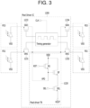
- FIG. 3 is a circuit diagram illustrating a pixel driving micro integrated chip in accordance with at least one embodiment.
- pixel driving micro integrated chip 1200 may be coupled to first photodiode PD1, second photodiode PD2, third photodiode PD3, and four photodiode PD4 and sequentially control four photodiodes PD1, PD2, PD3, and PD4.
- pixel driving micro integrated chip 1200 may sequentially turn on corresponding switches of first to four photodiode PD1 to PD4, sequentially read data accumulated in first to four photodiodes PD1 to PD4, and sequentially output read data to data driver circuit 13, in accordance with at least one embodiment.
- pixel driving micro integrated chip 1200 may include timing generator 1210, pixel driver transistor (TR) 1220, and four switches 1231 to 1234.
- pixel driving micro integrated chip 1200 may be electrically coupled to first photodiode PD1 through first switch 1231, electrically coupled to second photodiode PD2 through second switch 1232, electrically coupled to third photodiode PD3 through third switch 1233, and electrically coupled to fourth photodiode PD4 through fourth switch 1234.
- Timing generator 1210 may receive a clock signal (CLK), for example, from gate driver circuit 12 and generate a timing signal to sequentially switch first to fourth switches 1231 to 1234.
- CLK clock signal
- timing generator 1210 may be implemented with a digital counter or a shift register.
- a 2-bit counter may be used to minimize an IC size.
- Pixel driver transistor (TR) 1220 may read data from one of photodiodes PD1to PD4 which is switched on by the timing signal from timing generator 1210 and output the data to data driver circuit 13.
- Such pixel driver transistor (TR) 1220 may be implemented in a three transistor (3T) structure or a four transistor (4T) structure.
- X-ray detector 10 minimizes metal lines coupled to pixels and driver circuits. Accordingly, the above-described structure improves a fill factor, simplifies a manufacturing process, and reduces a unit manufacturing price in accordance with at least one embodiment.
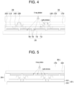
- FIG. 4 is a cross sectional view of a predetermined section in a pixel area of an X-ray detector in accordance with one embodiment of the present disclosure.
- FIG. 4 shows a predetermined part of a pixel area of a front side illumination type X-ray detector according to one embodiment.
- the pixel area of the X-ray detector may include three major layers, photodiode layer 100, driver layer 200, and scintillator layer 300.
- photodiode layer 100 may include common electrode 720 formed on insulating substrate 710, a plurality of photodiodes 730 arranged on common electrode 720 in matrix, and top transparent pixel electrode 740.
- insulating substrate 710 may be a glass substrate.
- a plurality of photodiodes 730 may receive visible light photons and convert light photons into an electrical signal.
- Such photodiode 730 may have a PIN diode structure including a P+ type region (e.g., high-concentration P type), a I type region, and an N type region.
- the P type photoconductive material may be CdTe.
- Such photodiode layer 100 may be manufactured using a TFT process in accordance with at least one embodiment. Accordingly, photodiode layer 100 may be manufactured as a large surface X-ray detector with a comparatively low manufacturing price. Furthermore, such photodiode layer 100 may be manufactured as a continuous layer for a comparatively low manufacturing price. Alternatively, photodiode layer 100 may be formed in an island array structure by patterning the continuous photodiode layer. In this case, such a structure may minimize crosstalk between adjacent photodiodes.
- Driver layer 200 may include a plurality of pixel driving ICs 1200 each controlling at least two of photodiodes and metal contacts connecting pixel driving ICs to corresponding photodiodes 730.
- one pixel driving IC 1200 sequentially or simultaneously controls four photodiodes.
- the number of photodiodes controlled by one pixel driving IC 1200 may be vary according to various factors related to the X-ray detector.
- FIG. 5 is a cross sectional view of a predetermined section in a pixel area of an X-ray detector in accordance with another embodiment of the present disclosure.
- FIG. 5 shows a predetermined part of a pixel area of a back side (BS) illumination type X-ray detector according to one embodiment.
- the pixel area of the X-ray detector may include driver layer 200-1, photodiode layer 100-1, and scintillator layer 300-1.
- Each of driver layer 200-1, photodiode layer 100-1,and scintillator layer 300-1 of the BS illumination type X-ray detector may have a structure similar to corresponding layers of the FS illumination type X-ray detector.
- photodiode layer 100-1 may be presented on driver layer 200-1 in the BS illumination type X-ray detector. That is, driver layer 200-1 and photodiode layer 100-1 of FIG. 5 may be upside down photodiode layer 100 and driver layer 200 of FIG. 4 .
- driver layer 200-1 is formed on photodiode layer 100-1, and the resultant of driver layer 200-1 and photodiode layer 100-1 is flipped in accordance with at least one embodiment. Then, the resultant may be placed on adhesive layer 1910 on carrier substrate 1920.
- the common electrode of photodiode layer 100-1 is the upper most layer of photodiode layer 100-1, and pixel driver micro IC 1200 is presented in the bottom most layer.
- metal contact lines and pixel driver micro IC do not block photodiodes 730 in accordance with at least one embodiment. Accordingly, the BS illustration type X-ray detector may deliver light photons to photodiode 730 without loss.
- insulating substrate 710 may be removed using a laser lift off technology, and barrier layer 1820 and scintillator layer 1720 are formed on photodiode layer 100-2 using material having flexible property. Accordingly, the durability and the flexibility of X-ray detector may be improved.
- photodiode layer 100-1 may be manufactured using a TFT process in accordance with at least one embodiment. Accordingly, photodiode layer 100-1 may be manufactured as a large surface X-ray detector with a comparatively low manufacturing price. Furthermore, such photodiode layer 100-1 may be manufactured as a continuous layer for a comparatively low manufacturing price. Alternatively, photodiode layer 100-1 may be formed in an island array structure by patterning the continuous photodiode layer. In this case, such a structure may minimize crosstalk between adjacent photodiodes.
- driver layer 200-1 may include a plurality of pixel driving ICs 1200 each controlling at least two of photodiodes and metal contacts connecting pixel driving ICs to corresponding photodiodes 730.
- one pixel driving IC 1200 sequentially or simultaneously controls four photodiodes.
- the number of photodiodes controlled by one pixel driving IC 1200 may be vary according to various factors related to the X-ray detector.
- a plurality of pixel driving ICs 1200 are manufactured separately from the photodiode layer 100 and printed on photodiode layer 100 using the micro-transfer printing technology after forming contact holes in photodiode layer 100. Then, metal contacts 140 are formed to connect pixel driving ICs 1200 to corresponding photodiodes 730.
- the plurality of pixel driving ICs 1200 may be manufactured using a CMOS process and printed on photodiode layer 100 using the micro-transfer technology. Accordingly, pixel driving ICs 1200 may be manufactured with high precision (e.g., nanometer level) to have a high image quality.
- scintillator layer 300-1 may be formed on photodiode layer 100-1. Such scintillator layer 300-1 may convert X-rays into visible light. Scintillator layer 300-1 may include scintillator 1720 and barrier layer 1820 and be made of material having flexible properties. Scintillator layer 300 may be formed of CsI or Gadox (Gd2O2:Tb).
- FIG. 6 is a flowchart illustrating a method of manufacturing an X-ray detector according to at least one embodiment of the present disclosure.
- FIGS. 7 to 17 are cross-sectional views for describing a method of manufacturing a front side illumination type X-ray detector in accordance with at least one embodiment.
- FIGS. 18 to 20 are cross-sectional views for describing a method of manufacturing a back side illumination type X-ray detector in accordance with at least one embodiment.
- photodiode layer 100 may be formed at step 6010.
- a plurality of photodiodes 730 may be formed on insulating substrate 710 at step S6010.
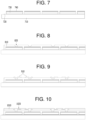
- FIG. 7 illustrates a process of forming a photodiode layer in accordance with at least one embodiment.
- common bottom electrode 720 may be formed on insulating substrate 710.
- Insulating substrate 710 may be made of material having flexible property.
- Common bottom electrode 720 may be made of indium tin oxide (ITO) or indium zinc oxide (IZO).
- Common bottom electrode 720 may be an ITO glass substrate or an IZO glass substrate, but the embodiments of the present disclosure are not limited thereto.
- common bottom electrode 720 may be a transparent layer for a back side illumination type X-ray detector.
- common bottom electrode 720 may be not a transparent layer for a front side illumination type X-ray detector.
- On common bottom electrode 720 a plurality of photodiodes 730 are formed.
- Photodiodes 730 may be made of amorphous silicon (a-Si) or organic silicon. Photodiodes 730 may be formed by forming a i-Si layer on common bottom electrode 720, forming a p-Si layer on the i-Si layer, and forming an n-Si layer on the p-Si layer.
- a-Si amorphous silicon
- Photodiodes 730 may be made of amorphous silicon (a-Si) or organic silicon. Photodiodes 730 may be formed by forming a i-Si layer on common bottom electrode 720, forming a p-Si layer on the i-Si layer, and forming an n-Si layer on the p-Si layer.
- Top transparent pixel electrode 740 may be formed on photodiodes 730.
- Top transparent pixel electrode 740 may be made of indium tin oxide (ITO) or indium zinc oxide (IZO).
- Top transparent pixel electrode 740 may be an ITO glass substrate or an IZO glass substrate, but the embodiments of the present disclosure are not limited thereto.
- Top transparent pixel electrode 740 may be a transparent layer for a front side illumination type X-ray detector.
- Top transparent pixel electrode 740 may be not a transparent layer for a back side illumination type X-ray detector.
- photodiode layer 100 may be formed using the TFT process in accordance with at least one embodiment.
- Photodiode layer 100 may be formed as a continuous layer, thereby minimizing a unit manufacturing price. Furthermore, photodiode layer 100 may be formed in an Island array structure through patterning. That is, as shown, a plurality of photodiodes 730 is formed thereon in a form of matrix. In this case, the crosstalk between adjacent photodiodes may be minimized.
- driver layer 200 may be formed on photodiode layer 100 at steps S6020 to S6050.
- FIG. 8 to FIG. 14 are diagrams illustrating a procedure of forming a driving layer on a photodiode layer in accordance with at least one embodiment.
- first inter layer dielectric (ILD) layer 810 (e.g., ILD1) may be formed on photodiode layer 100 to cover all photodiodes 730 and gaps between adjacent pixels, and a plurality of metal contact holes 820 may be formed in first ILD1 layer 810 as shown in FIG. 8 .
- one metal contact hole 820 may be formed on each photodiode to expose top transparent pixel electrode 740.
- first metal contact layer 910 may be formed to fill first contact hole 820 and to extend along the top surface of ILD1 layer 810 in predetermined length, as shown in FIG. 9 .
- second ILD layer 1010 may be formed on metal contact layer 910 and first ILD layer 810 (ILD1), and second contact holes 1020 may be formed at each photodiode 730 in second ILD layer 1010 (ILD2) to expose corresponding first metal contact layer 910, as shown in FIG. 10 .
- print adhesive layer 1110 may be formed on second ILD layer 1010 (ILD2) and second contact holes 1020, as shown in FIG. 11 .
- Print adhesive layer 1101 may be made of resin and a thickness of about 1.2 um.
- Print adhesive layer 1101 may be formed for printing pixel driving integrated chips (ICs) 1200 thereon. That is, print adhesive layer 1101 on photodiode layer 100 may be a target panel.
- ICs integrated chips
- pixel driving integrated chips (ICs) 1200 may be printed on print adhesive layer 1100.
- Each pixel driving IC may be positioned between two adjacent pixels, as shown in FIG. 12 .
- each pixel driving IC may be position to sequentially control corresponding four photodiodes in accordance with at least one embodiment.
- FIG. 21 shows a micro transfer printing process for printing a plurality of pixel driving micro integrated chips on a photodiode layer in accordance with at least one embodiment.
- pixel driving integrated chips (ICs) 1200 may be fabricated in source silicon wafer 2510.
- a CMOS process may be performed in order to fabricate an IC with high precision (e.g., micrometer level) to provide a high image quality.
- pixel driving integrated chips (ICs) 1200 on source silicon wafer 2510 may be transferred onto elastomer stamp 2520.
- pixel driving integrated chips 1200 may be printed on print adhesive layer 1101 on photodiode layer 100 by pressing elastomer stamp 2520 on target panel 2530 (e.g., print adhesive layer 1101 on photodiode layer 100) with predetermined conditions.
- elastomer stamp 2520 may be removed after printing.
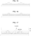
- third contact holes 1300 may be formed at both sides of each pixel driving IC 1200 to expose first metal contact layer 910 through second ILD2 layer 1010 and print adhesive layer 1110, as shown in FIG. 13 .
- pixel driving IC 1200 may be formed directly on first ILD layer 810 and connected to corresponding photodiodes 720 without forming second ILD layer 1010 and print adhesive layer 1110 when first ILD layer 810 has moisture proofing priority and adhesive priority, as shown in FIG. 15 .
- a manufacturing method may be further simplified.
- pixel driving IC 1200 may be formed directly on second ILD 2 layer 1010 and connected to corresponding pixels 730 without forming print adhesive layer 1110 when second ILD 2 layer 1010 has moisture proofing priority and adhesive priority, as shown in FIG. 16 .
- surface passivation layer 1710 is formed on print adhesive layer 1110 and pixel driving ICs 1200 at step S6090.
- Scintillator layer 1720 may be formed on the surface passivation layer 1610 at step S6100, as shown in FIG. 17 .
- pixel area 111 of front side illumination X-ray detector 10 may be completely manufactured.
- X-ray detector 10 may be manufactured as a back side illumination type X-ray detector in accordance with another embodiment. Hereinafter, a method for manufacturing a pixel area of the back side illumination type X-ray detector will be described with reference to FIG 18 to FIG. 20 .
- FIG. 18 to FIG. 20 are cross-sectional views schematically illustrating a process of manufacturing a back side illumination type X-ray detector in accordance with at least one embodiment.
- a sacrificing layer 1810 is formed on insulating substrate 710, and a barrier layer 1820 is formed on the sacrificing layer 1810 at step S6010.
- the sacrificing layer 1810 is formed for laser lift off (LLO).
- the barrier layer 1820 is made of PI. After forming the barrier layer 1820, photodiode layer 100 and driving layer 200 may be formed on the barrier layer 1820 similar to processes shown in FIG. 7 to FIG. 14 .
- a laser lift-off process may be performed for removing the glass layer 710 and the sacrificing layer 1810 at step S6110 as shown in FIG. 18 . Since glass layer 710 is remove, the durability of X-ray detector 10 may be enhanced in accordance with at least one embodiment.
- a flipping process is performed for flipping the resultant of photodiode layer 100 and driving layer 200 at step S6120 and placed on adhesive layer 1910 formed on carrier substate 1920 made of a carbon graphite at step S6130.
- scintillator layer 1720 is formed on barrier layer 1820 at S6130.
- the pixel area of back side illumination type X-ray detector may be formed completely.
- exemplary is used herein to mean serving as an example, instance, or illustration. Any aspect or design described herein as "exemplary” is not necessarily to be construed as preferred or advantageous over other aspects or designs. Rather, use of the word exemplary is intended to present concepts in a concrete fashion.
- a component may be, but is not limited to being, a process running on a processor, a processor, an object, an executable, a thread of execution, a program, and/or a computer.
- an application running on a controller and the controller can be a component.
- One or more components may reside within a process and/or thread of execution and a component may be localized on one computer and/or distributed between two or more computers.
- the present invention can be embodied in the form of methods and apparatuses for practicing those methods.
- the present invention can also be embodied in the form of program code embodied in tangible media, non-transitory media, such as magnetic recording media, optical recording media, solid state memory, floppy diskettes, CD-ROMs, hard drives, or any other machine-readable storage medium, wherein, when the program code is loaded into and executed by a machine, such as a computer, the machine becomes an apparatus for practicing the invention.
- the present invention can also be embodied in the form of program code, for example, whether stored in a storage medium, loaded into and/or executed by a machine, or transmitted over some transmission medium or carrier, such as over electrical wiring or cabling, through fiber optics, or via electromagnetic radiation, wherein, when the program code is loaded into and executed by a machine, such as a computer, the machine becomes an apparatus for practicing the invention.
- program code When implemented on a general-purpose processor, the program code segments combine with the processor to provide a unique device that operates analogously to specific logic circuits.
- the present invention can also be embodied in the form of a bitstream or other sequence of signal values electrically or optically transmitted through a medium, stored magnetic-field variations in a magnetic recording medium, etc., generated using a method and/or an apparatus of the present invention.
- the term "compatible" means that the element communicates with other elements in a manner wholly or partially specified by the standard, and would be recognized by other elements as sufficiently capable of communicating with the other elements in the manner specified by the standard.
- the compatible element does not need to operate internally in a manner specified by the standard.
Landscapes
- Health & Medical Sciences (AREA)
- Physics & Mathematics (AREA)
- Spectroscopy & Molecular Physics (AREA)
- Life Sciences & Earth Sciences (AREA)
- General Physics & Mathematics (AREA)
- High Energy & Nuclear Physics (AREA)
- Molecular Biology (AREA)
- Engineering & Computer Science (AREA)
- Mechanical Engineering (AREA)
- Biomedical Technology (AREA)
- General Health & Medical Sciences (AREA)
- Medical Informatics (AREA)
- Nuclear Medicine, Radiotherapy & Molecular Imaging (AREA)
- Optics & Photonics (AREA)
- Measurement Of Radiation (AREA)
- Solid State Image Pick-Up Elements (AREA)
- Light Receiving Elements (AREA)
- Toxicology (AREA)
Applications Claiming Priority (1)
| Application Number | Priority Date | Filing Date | Title |
|---|---|---|---|
| US16/731,007 US11194063B2 (en) | 2019-12-30 | 2019-12-30 | X-ray detector having driver micro integrated chips printed on photodiode layer |
Publications (2)
| Publication Number | Publication Date |
|---|---|
| EP3846211A1 EP3846211A1 (en) | 2021-07-07 |
| EP3846211B1 true EP3846211B1 (en) | 2024-12-11 |
Family
ID=70058224
Family Applications (1)
| Application Number | Title | Priority Date | Filing Date |
|---|---|---|---|
| EP20166711.0A Active EP3846211B1 (en) | 2019-12-30 | 2020-03-30 | System to operate x-ray detector having driver micro integrated chips printed on photodiode layer |
Country Status (5)
| Country | Link |
|---|---|
| US (1) | US11194063B2 (enExample) |
| EP (1) | EP3846211B1 (enExample) |
| JP (1) | JP7633021B6 (enExample) |
| KR (1) | KR102520453B1 (enExample) |
| CN (1) | CN113130524B (enExample) |
Families Citing this family (2)
| Publication number | Priority date | Publication date | Assignee | Title |
|---|---|---|---|---|
| CN114823745B (zh) * | 2021-01-28 | 2024-10-29 | 睿生光电股份有限公司 | X射线装置 |
| US20240241272A1 (en) * | 2023-01-17 | 2024-07-18 | GE Precision Healthcare LLC | Flat panel x-ray detector for computed tomography |
Family Cites Families (19)
| Publication number | Priority date | Publication date | Assignee | Title |
|---|---|---|---|---|
| US5464984A (en) * | 1985-12-11 | 1995-11-07 | General Imaging Corporation | X-ray imaging system and solid state detector therefor |
| JP4205134B2 (ja) * | 1998-02-09 | 2009-01-07 | シャープ株式会社 | 二次元画像検出器 |
| TW417383B (en) * | 1998-07-01 | 2001-01-01 | Cmos Sensor Inc | Silicon butting contact image sensor chip with line transfer and pixel readout (LTPR) structure |
| US6510195B1 (en) * | 2001-07-18 | 2003-01-21 | Koninklijke Philips Electronics, N.V. | Solid state x-radiation detector modules and mosaics thereof, and an imaging method and apparatus employing the same |
| DE10142531A1 (de) * | 2001-08-30 | 2003-03-20 | Philips Corp Intellectual Pty | Sensoranordnung aus licht- und/oder röntgenstrahlungsempfindlichen Sensoren |
| EP2142943A2 (en) * | 2007-04-23 | 2010-01-13 | Koninklijke Philips Electronics N.V. | Detector with a partially transparent scintillator substrate |
| JP5172267B2 (ja) * | 2007-10-09 | 2013-03-27 | 富士フイルム株式会社 | 撮像装置 |
| JP5281484B2 (ja) * | 2009-05-28 | 2013-09-04 | 浜松ホトニクス株式会社 | 放射線検出ユニット |
| JP5467846B2 (ja) * | 2009-11-20 | 2014-04-09 | 富士フイルム株式会社 | 放射線検出素子 |
| KR20140092438A (ko) * | 2012-12-27 | 2014-07-24 | 삼성전자주식회사 | 엑스선 검출 패널, 엑스선 촬영 장치 및 엑스선 영상 생성 방법 |
| US9354186B2 (en) * | 2013-03-13 | 2016-05-31 | Texas Instruments Incorporated | X-ray sensor and signal processing assembly for an X-ray computed tomography machine |
| US9324747B2 (en) | 2014-03-13 | 2016-04-26 | Semiconductor Energy Laboratory Co., Ltd. | Imaging device |
| US20160020131A1 (en) * | 2014-07-20 | 2016-01-21 | X-Celeprint Limited | Apparatus and methods for micro-transfer-printing |
| JP2016039203A (ja) * | 2014-08-06 | 2016-03-22 | ソニー株式会社 | 機能性素子および電子機器 |
| US10050076B2 (en) | 2014-10-07 | 2018-08-14 | Terapede Systems Inc. | 3D high resolution X-ray sensor with integrated scintillator grid |
| US9640715B2 (en) | 2015-05-15 | 2017-05-02 | X-Celeprint Limited | Printable inorganic semiconductor structures |
| US9905607B2 (en) * | 2015-07-28 | 2018-02-27 | General Electric Company | Radiation detector fabrication |
| CN207587734U (zh) * | 2017-03-13 | 2018-07-06 | 泰拉派德系统股份有限公司 | 一种间接x射线传感器、直接x射线传感器和光学传感器 |
| US10832935B2 (en) * | 2017-08-14 | 2020-11-10 | X Display Company Technology Limited | Multi-level micro-device tethers |
-
2019
- 2019-12-30 US US16/731,007 patent/US11194063B2/en active Active
-
2020
- 2020-03-30 EP EP20166711.0A patent/EP3846211B1/en active Active
- 2020-12-25 JP JP2020217042A patent/JP7633021B6/ja active Active
- 2020-12-29 KR KR1020200185653A patent/KR102520453B1/ko active Active
- 2020-12-30 CN CN202011609021.5A patent/CN113130524B/zh active Active
Also Published As
| Publication number | Publication date |
|---|---|
| JP7633021B2 (ja) | 2025-02-19 |
| KR20210086981A (ko) | 2021-07-09 |
| EP3846211A1 (en) | 2021-07-07 |
| CN113130524B (zh) | 2024-12-27 |
| JP2021110741A (ja) | 2021-08-02 |
| JP7633021B6 (ja) | 2025-03-07 |
| US11194063B2 (en) | 2021-12-07 |
| US20210199817A1 (en) | 2021-07-01 |
| CN113130524A (zh) | 2021-07-16 |
| KR102520453B1 (ko) | 2023-06-08 |
Similar Documents
| Publication | Publication Date | Title |
|---|---|---|
| JP3607305B2 (ja) | 大領域能動マトリックス配列を製造する方法 | |
| JP3552233B2 (ja) | 周辺回路素子を集積化した画像形成ピクセル素子を有するピクセルアレイ | |
| JP3847494B2 (ja) | 二次元画像検出器の製造方法 | |
| CN102655159A (zh) | 大型x射线探测器 | |
| TWI357658B (en) | Solid-state imaging device and electronic device | |
| JP4147186B2 (ja) | 感光及び/又は感x線センサからなるセンサ配置 | |
| CN111354815B (zh) | 像素阵列面板与包括像素阵列面板的数字x射线检测器 | |
| US10283557B2 (en) | Radiation detector assembly | |
| JP3597392B2 (ja) | 二次元画像検出器 | |
| EP3846211B1 (en) | System to operate x-ray detector having driver micro integrated chips printed on photodiode layer | |
| KR20160047469A (ko) | 방사선 검출기, 방사선 검출기의 제조 방법, 촬상 장치, 및 촬상 표시 시스템 | |
| US20110073750A1 (en) | Image pickup apparatus and radiation image pickup system | |
| JP4205134B2 (ja) | 二次元画像検出器 | |
| CN102144176B (zh) | 具有转换片和互连层堆栈的辐射探测器的生产方法 | |
| US10686003B2 (en) | Radiation detector assembly | |
| CN100511693C (zh) | 辐射检测设备、辐射成像设备和辐射成像系统 | |
| US8508011B2 (en) | Semiconductor apparatus and method of manufacturing the same | |
| US11737722B2 (en) | X-ray detector having fabrication fault tolerant structure and fabrication method thereof | |
| JP4202315B2 (ja) | 二次元画像検出器 | |
| KR102686434B1 (ko) | 디지털 엑스레이 검출장치용 어레이 패널 및 이를 포함하는 디지털 엑스레이 검출장치 | |
| US20250081655A1 (en) | Light-sensitive matrix-array detector and process for producing the lightsensitive detector | |
| US20230345801A1 (en) | Display device | |
| KR102645331B1 (ko) | 디지털 엑스레이 검출장치용 어레이 패널 및 이를 포함하는 디지털 엑스레이 검출장치 | |
| KR20210083008A (ko) | 디지털 엑스레이 검출장치용 어레이 패널 및 이의 제조방법 | |
| JPH05160378A (ja) | 2次元イメージセンサ |
Legal Events
| Date | Code | Title | Description |
|---|---|---|---|
| PUAI | Public reference made under article 153(3) epc to a published international application that has entered the european phase |
Free format text: ORIGINAL CODE: 0009012 |
|
| STAA | Information on the status of an ep patent application or granted ep patent |
Free format text: STATUS: THE APPLICATION HAS BEEN PUBLISHED |
|
| AK | Designated contracting states |
Kind code of ref document: A1 Designated state(s): AL AT BE BG CH CY CZ DE DK EE ES FI FR GB GR HR HU IE IS IT LI LT LU LV MC MK MT NL NO PL PT RO RS SE SI SK SM TR |
|
| STAA | Information on the status of an ep patent application or granted ep patent |
Free format text: STATUS: REQUEST FOR EXAMINATION WAS MADE |
|
| 17P | Request for examination filed |
Effective date: 20220107 |
|
| RBV | Designated contracting states (corrected) |
Designated state(s): AL AT BE BG CH CY CZ DE DK EE ES FI FR GB GR HR HU IE IS IT LI LT LU LV MC MK MT NL NO PL PT RO RS SE SI SK SM TR |
|
| GRAP | Despatch of communication of intention to grant a patent |
Free format text: ORIGINAL CODE: EPIDOSNIGR1 |
|
| STAA | Information on the status of an ep patent application or granted ep patent |
Free format text: STATUS: GRANT OF PATENT IS INTENDED |
|
| INTG | Intention to grant announced |
Effective date: 20240711 |
|
| GRAS | Grant fee paid |
Free format text: ORIGINAL CODE: EPIDOSNIGR3 |
|
| GRAA | (expected) grant |
Free format text: ORIGINAL CODE: 0009210 |
|
| STAA | Information on the status of an ep patent application or granted ep patent |
Free format text: STATUS: THE PATENT HAS BEEN GRANTED |
|
| REG | Reference to a national code |
Ref country code: DE Ref legal event code: R079 Ref document number: 602020042855 Country of ref document: DE Free format text: PREVIOUS MAIN CLASS: H01L0027146000 Ipc: H10F0039180000 |
|
| AK | Designated contracting states |
Kind code of ref document: B1 Designated state(s): AL AT BE BG CH CY CZ DE DK EE ES FI FR GB GR HR HU IE IS IT LI LT LU LV MC MK MT NL NO PL PT RO RS SE SI SK SM TR |
|
| REG | Reference to a national code |
Ref country code: GB Ref legal event code: FG4D |
|
| REG | Reference to a national code |
Ref country code: CH Ref legal event code: EP |
|
| REG | Reference to a national code |
Ref country code: IE Ref legal event code: FG4D |
|
| REG | Reference to a national code |
Ref country code: DE Ref legal event code: R096 Ref document number: 602020042855 Country of ref document: DE |
|
| REG | Reference to a national code |
Ref country code: LT Ref legal event code: MG9D |
|
| PG25 | Lapsed in a contracting state [announced via postgrant information from national office to epo] |
Ref country code: HR Free format text: LAPSE BECAUSE OF FAILURE TO SUBMIT A TRANSLATION OF THE DESCRIPTION OR TO PAY THE FEE WITHIN THE PRESCRIBED TIME-LIMIT Effective date: 20241211 |
|
| PG25 | Lapsed in a contracting state [announced via postgrant information from national office to epo] |
Ref country code: FI Free format text: LAPSE BECAUSE OF FAILURE TO SUBMIT A TRANSLATION OF THE DESCRIPTION OR TO PAY THE FEE WITHIN THE PRESCRIBED TIME-LIMIT Effective date: 20241211 |
|
| PG25 | Lapsed in a contracting state [announced via postgrant information from national office to epo] |
Ref country code: BG Free format text: LAPSE BECAUSE OF FAILURE TO SUBMIT A TRANSLATION OF THE DESCRIPTION OR TO PAY THE FEE WITHIN THE PRESCRIBED TIME-LIMIT Effective date: 20241211 |
|
| REG | Reference to a national code |
Ref country code: NL Ref legal event code: MP Effective date: 20241211 |
|
| PG25 | Lapsed in a contracting state [announced via postgrant information from national office to epo] |
Ref country code: ES Free format text: LAPSE BECAUSE OF FAILURE TO SUBMIT A TRANSLATION OF THE DESCRIPTION OR TO PAY THE FEE WITHIN THE PRESCRIBED TIME-LIMIT Effective date: 20241211 |
|
| PG25 | Lapsed in a contracting state [announced via postgrant information from national office to epo] |
Ref country code: NO Free format text: LAPSE BECAUSE OF FAILURE TO SUBMIT A TRANSLATION OF THE DESCRIPTION OR TO PAY THE FEE WITHIN THE PRESCRIBED TIME-LIMIT Effective date: 20250311 |
|
| PG25 | Lapsed in a contracting state [announced via postgrant information from national office to epo] |
Ref country code: GR Free format text: LAPSE BECAUSE OF FAILURE TO SUBMIT A TRANSLATION OF THE DESCRIPTION OR TO PAY THE FEE WITHIN THE PRESCRIBED TIME-LIMIT Effective date: 20250312 Ref country code: LV Free format text: LAPSE BECAUSE OF FAILURE TO SUBMIT A TRANSLATION OF THE DESCRIPTION OR TO PAY THE FEE WITHIN THE PRESCRIBED TIME-LIMIT Effective date: 20241211 |
|
| PG25 | Lapsed in a contracting state [announced via postgrant information from national office to epo] |
Ref country code: RS Free format text: LAPSE BECAUSE OF FAILURE TO SUBMIT A TRANSLATION OF THE DESCRIPTION OR TO PAY THE FEE WITHIN THE PRESCRIBED TIME-LIMIT Effective date: 20250311 |
|
| PG25 | Lapsed in a contracting state [announced via postgrant information from national office to epo] |
Ref country code: NL Free format text: LAPSE BECAUSE OF FAILURE TO SUBMIT A TRANSLATION OF THE DESCRIPTION OR TO PAY THE FEE WITHIN THE PRESCRIBED TIME-LIMIT Effective date: 20241211 |
|
| REG | Reference to a national code |
Ref country code: AT Ref legal event code: MK05 Ref document number: 1751093 Country of ref document: AT Kind code of ref document: T Effective date: 20241211 |
|
| PG25 | Lapsed in a contracting state [announced via postgrant information from national office to epo] |
Ref country code: SM Free format text: LAPSE BECAUSE OF FAILURE TO SUBMIT A TRANSLATION OF THE DESCRIPTION OR TO PAY THE FEE WITHIN THE PRESCRIBED TIME-LIMIT Effective date: 20241211 |
|
| PG25 | Lapsed in a contracting state [announced via postgrant information from national office to epo] |
Ref country code: PL Free format text: LAPSE BECAUSE OF FAILURE TO SUBMIT A TRANSLATION OF THE DESCRIPTION OR TO PAY THE FEE WITHIN THE PRESCRIBED TIME-LIMIT Effective date: 20241211 |
|
| PGFP | Annual fee paid to national office [announced via postgrant information from national office to epo] |
Ref country code: DE Payment date: 20250407 Year of fee payment: 6 |
|
| PGFP | Annual fee paid to national office [announced via postgrant information from national office to epo] |
Ref country code: GB Payment date: 20250407 Year of fee payment: 6 |
|
| PG25 | Lapsed in a contracting state [announced via postgrant information from national office to epo] |
Ref country code: IS Free format text: LAPSE BECAUSE OF FAILURE TO SUBMIT A TRANSLATION OF THE DESCRIPTION OR TO PAY THE FEE WITHIN THE PRESCRIBED TIME-LIMIT Effective date: 20250411 |
|
| PG25 | Lapsed in a contracting state [announced via postgrant information from national office to epo] |
Ref country code: PT Free format text: LAPSE BECAUSE OF FAILURE TO SUBMIT A TRANSLATION OF THE DESCRIPTION OR TO PAY THE FEE WITHIN THE PRESCRIBED TIME-LIMIT Effective date: 20250411 |
|
| PG25 | Lapsed in a contracting state [announced via postgrant information from national office to epo] |
Ref country code: EE Free format text: LAPSE BECAUSE OF FAILURE TO SUBMIT A TRANSLATION OF THE DESCRIPTION OR TO PAY THE FEE WITHIN THE PRESCRIBED TIME-LIMIT Effective date: 20241211 |
|
| PG25 | Lapsed in a contracting state [announced via postgrant information from national office to epo] |
Ref country code: RO Free format text: LAPSE BECAUSE OF FAILURE TO SUBMIT A TRANSLATION OF THE DESCRIPTION OR TO PAY THE FEE WITHIN THE PRESCRIBED TIME-LIMIT Effective date: 20241211 Ref country code: AT Free format text: LAPSE BECAUSE OF FAILURE TO SUBMIT A TRANSLATION OF THE DESCRIPTION OR TO PAY THE FEE WITHIN THE PRESCRIBED TIME-LIMIT Effective date: 20241211 |
|
| PG25 | Lapsed in a contracting state [announced via postgrant information from national office to epo] |
Ref country code: SK Free format text: LAPSE BECAUSE OF FAILURE TO SUBMIT A TRANSLATION OF THE DESCRIPTION OR TO PAY THE FEE WITHIN THE PRESCRIBED TIME-LIMIT Effective date: 20241211 |
|
| PG25 | Lapsed in a contracting state [announced via postgrant information from national office to epo] |
Ref country code: CZ Free format text: LAPSE BECAUSE OF FAILURE TO SUBMIT A TRANSLATION OF THE DESCRIPTION OR TO PAY THE FEE WITHIN THE PRESCRIBED TIME-LIMIT Effective date: 20241211 |
|
| PG25 | Lapsed in a contracting state [announced via postgrant information from national office to epo] |
Ref country code: IT Free format text: LAPSE BECAUSE OF FAILURE TO SUBMIT A TRANSLATION OF THE DESCRIPTION OR TO PAY THE FEE WITHIN THE PRESCRIBED TIME-LIMIT Effective date: 20241211 |
|
| PG25 | Lapsed in a contracting state [announced via postgrant information from national office to epo] |
Ref country code: SE Free format text: LAPSE BECAUSE OF FAILURE TO SUBMIT A TRANSLATION OF THE DESCRIPTION OR TO PAY THE FEE WITHIN THE PRESCRIBED TIME-LIMIT Effective date: 20241211 |
|
| REG | Reference to a national code |
Ref country code: DE Ref legal event code: R097 Ref document number: 602020042855 Country of ref document: DE |
|
| PG25 | Lapsed in a contracting state [announced via postgrant information from national office to epo] |
Ref country code: DK Free format text: LAPSE BECAUSE OF FAILURE TO SUBMIT A TRANSLATION OF THE DESCRIPTION OR TO PAY THE FEE WITHIN THE PRESCRIBED TIME-LIMIT Effective date: 20241211 |
|
| PG25 | Lapsed in a contracting state [announced via postgrant information from national office to epo] |
Ref country code: MC Free format text: LAPSE BECAUSE OF FAILURE TO SUBMIT A TRANSLATION OF THE DESCRIPTION OR TO PAY THE FEE WITHIN THE PRESCRIBED TIME-LIMIT Effective date: 20241211 |
|
| PLBE | No opposition filed within time limit |
Free format text: ORIGINAL CODE: 0009261 |
|
| STAA | Information on the status of an ep patent application or granted ep patent |
Free format text: STATUS: NO OPPOSITION FILED WITHIN TIME LIMIT |
|
| REG | Reference to a national code |
Ref country code: CH Ref legal event code: L10 Free format text: ST27 STATUS EVENT CODE: U-0-0-L10-L00 (AS PROVIDED BY THE NATIONAL OFFICE) Effective date: 20251022 |
|
| REG | Reference to a national code |
Ref country code: CH Ref legal event code: H13 Free format text: ST27 STATUS EVENT CODE: U-0-0-H10-H13 (AS PROVIDED BY THE NATIONAL OFFICE) Effective date: 20251023 |
|
| PG25 | Lapsed in a contracting state [announced via postgrant information from national office to epo] |
Ref country code: LU Free format text: LAPSE BECAUSE OF NON-PAYMENT OF DUE FEES Effective date: 20250330 |
|
| 26N | No opposition filed |
Effective date: 20250912 |