EP3832191B1 - Method for manufacturing light emitting diode filament - Google Patents
Method for manufacturing light emitting diode filament Download PDFInfo
- Publication number
- EP3832191B1 EP3832191B1 EP20151385.0A EP20151385A EP3832191B1 EP 3832191 B1 EP3832191 B1 EP 3832191B1 EP 20151385 A EP20151385 A EP 20151385A EP 3832191 B1 EP3832191 B1 EP 3832191B1
- Authority
- EP
- European Patent Office
- Prior art keywords
- bracket
- metal sheet
- metal sheets
- led chips
- led
- Prior art date
- Legal status (The legal status is an assumption and is not a legal conclusion. Google has not performed a legal analysis and makes no representation as to the accuracy of the status listed.)
- Active
Links
Images




Classifications
-
- F—MECHANICAL ENGINEERING; LIGHTING; HEATING; WEAPONS; BLASTING
- F21—LIGHTING
- F21K—NON-ELECTRIC LIGHT SOURCES USING LUMINESCENCE; LIGHT SOURCES USING ELECTROCHEMILUMINESCENCE; LIGHT SOURCES USING CHARGES OF COMBUSTIBLE MATERIAL; LIGHT SOURCES USING SEMICONDUCTOR DEVICES AS LIGHT-GENERATING ELEMENTS; LIGHT SOURCES NOT OTHERWISE PROVIDED FOR
- F21K9/00—Light sources using semiconductor devices as light-generating elements, e.g. using light-emitting diodes [LED] or lasers
- F21K9/90—Methods of manufacture
-
- H—ELECTRICITY
- H10—SEMICONDUCTOR DEVICES; ELECTRIC SOLID-STATE DEVICES NOT OTHERWISE PROVIDED FOR
- H10H—INORGANIC LIGHT-EMITTING SEMICONDUCTOR DEVICES HAVING POTENTIAL BARRIERS
- H10H20/00—Individual inorganic light-emitting semiconductor devices having potential barriers, e.g. light-emitting diodes [LED]
- H10H20/80—Constructional details
- H10H20/85—Packages
- H10H20/852—Encapsulations
-
- H—ELECTRICITY
- H10—SEMICONDUCTOR DEVICES; ELECTRIC SOLID-STATE DEVICES NOT OTHERWISE PROVIDED FOR
- H10H—INORGANIC LIGHT-EMITTING SEMICONDUCTOR DEVICES HAVING POTENTIAL BARRIERS
- H10H20/00—Individual inorganic light-emitting semiconductor devices having potential barriers, e.g. light-emitting diodes [LED]
- H10H20/80—Constructional details
- H10H20/85—Packages
- H10H20/852—Encapsulations
- H10H20/854—Encapsulations characterised by their material, e.g. epoxy or silicone resins
-
- H—ELECTRICITY
- H10—SEMICONDUCTOR DEVICES; ELECTRIC SOLID-STATE DEVICES NOT OTHERWISE PROVIDED FOR
- H10H—INORGANIC LIGHT-EMITTING SEMICONDUCTOR DEVICES HAVING POTENTIAL BARRIERS
- H10H20/00—Individual inorganic light-emitting semiconductor devices having potential barriers, e.g. light-emitting diodes [LED]
- H10H20/80—Constructional details
- H10H20/85—Packages
- H10H20/857—Interconnections, e.g. lead-frames, bond wires or solder balls
-
- H—ELECTRICITY
- H10—SEMICONDUCTOR DEVICES; ELECTRIC SOLID-STATE DEVICES NOT OTHERWISE PROVIDED FOR
- H10W—GENERIC PACKAGES, INTERCONNECTIONS, CONNECTORS OR OTHER CONSTRUCTIONAL DETAILS OF DEVICES COVERED BY CLASS H10
- H10W90/00—Package configurations
-
- H—ELECTRICITY
- H10—SEMICONDUCTOR DEVICES; ELECTRIC SOLID-STATE DEVICES NOT OTHERWISE PROVIDED FOR
- H10H—INORGANIC LIGHT-EMITTING SEMICONDUCTOR DEVICES HAVING POTENTIAL BARRIERS
- H10H20/00—Individual inorganic light-emitting semiconductor devices having potential barriers, e.g. light-emitting diodes [LED]
- H10H20/01—Manufacture or treatment
- H10H20/036—Manufacture or treatment of packages
- H10H20/0362—Manufacture or treatment of packages of encapsulations
-
- H—ELECTRICITY
- H10—SEMICONDUCTOR DEVICES; ELECTRIC SOLID-STATE DEVICES NOT OTHERWISE PROVIDED FOR
- H10H—INORGANIC LIGHT-EMITTING SEMICONDUCTOR DEVICES HAVING POTENTIAL BARRIERS
- H10H20/00—Individual inorganic light-emitting semiconductor devices having potential barriers, e.g. light-emitting diodes [LED]
- H10H20/01—Manufacture or treatment
- H10H20/036—Manufacture or treatment of packages
- H10H20/0364—Manufacture or treatment of packages of interconnections
Definitions
- the present disclosure relates to the field of light emitting diode (LED) filament, and more particularly to a method for manufacturing LED filaments.
- LED light emitting diode
- LED street lamps are almost direct current (DC) droved, that is, a mature switching power supply technology is used to turn the alternating current (AC) into DC to drive the LED filament.
- DC direct current
- AC alternating current
- Related prior art to the manufacturing of related filaments can be found in CN104600181A , CN205592683 U , EP2846083A1 , and CN110345505 A .
- DC driving has become a mainstream driving method since it can provide stable current for LED.
- the development of DC driving may be restricted by the bottlenecks of using life and cost. Simultaneously, it is very complicated to manufacture a DC droved filament, which further raises the cost.
- the present disclosure is to provide a method for manufacturing light emitting diode filament, which aims to solve the problem of complicated manufacturing process and high cost for the filament.
- the present disclosure provides a method for manufacturing an LED filament, according to claim 1, and the method includes the following operations S1 to S4.
- Operation S1 a plurality of metal sheets are provided and arranged at least two rows in parallel, each metal sheet at one row has one end extending to the corresponding metal sheet at the other row, and the other ends of each of the metal sheets connect with each other to form a positioning portion;
- operation S2 a plurality of brackets are provided, and each bracket is located between two corresponding metal sheets and fixedly connected to the two metal sheets;
- operation S3, a plurality of LED chips are provided and attached to each of the brackets, and the LED chips are electrically connected to the metal sheets by conducting wire; or, each bracket is prefabricated with conducting strip, and the LED chips are attached to the bracket and electrically connected to the metal sheets by the conducting strip;
- each bracket, the LED chips defined on the bracket, the conducting strip or the conducting wire defined on the bracket, and the joints of the bracket and the metal sheets are all cladded using packaging material to form an
- the method for manufacturing LED filament further includes operation S5, which cuts off the metal sheet at a position located between the positioning portion and the joint of the bracket and the metal sheet to obtain separate LED filaments.
- the positioning portion is defined with a plurality of positioning through holes.
- the plurality of positioning through holes are corresponding to each of the brackets.
- each metal sheet defines a clamping part for clamping the bracket.
- the clamping part includes a pair of clamping pieces facing and spaced from each other, the pair of clamping pieces are respectively bent and extended from opposite two sides of the metal sheet, the pair of clamping pieces and the metal sheet cooperatively form a receiving cavity, and the end of the bracket is received in the receiving cavity.
- each of the metal sheets in one row is defined with a marking hole.
- the metal sheet is cut off at the position located between the positioning through hole and the marking hole to obtain the LED filament.
- each bracket is attached with a rectifier module, and the rectifier module is defined at an end of the bracket closing to the metal sheet.
- the packaging material includes silicone, rubber, or resin.
- the bracket is made of ceramic or glass.
- the method for manufacturing LED filament can produce LED filament groups in batches, which simples the manufacturing process and reduces the cost. Further, the encapsulation layer may completely isolate the LED chips and the brackets from air, so that oxidation of the LED chips and the brackets may be avoided, and a good environment is provided for the LED chips to run well in a confined space. As such, the using life of the LED filament is also greatly improved.
- the method for manufacturing an LED filament according to the present disclosure includes the following operations.
- each metal sheet 10 at one row has one end extending to the corresponding metal sheet at the other row, and the other ends of each of the metal sheets connect with each other to form a positioning portion.
- the metal sheet 10 may be made of metal with good conductive properties.
- the metal sheet 10 may be obtained by dividing metal strips made in rolls into reasonable length, such as 120 millimeters or 144 millimeters.
- the two rows of metal sheet 10 may also be obtained by stamping an integral metal piece.
- the two rows of metal sheet 10 are arranged in parallel and spaced apart from each other, and each of the metal sheets 10 in a same row is aligned with each other.
- Each metal sheet 10 at one row has one end extending to the corresponding metal sheet 10 at the other row, and the other ends of the each metal sheet 10 connects with each other to form a positioning portion 20.
- the positioning portion 20 is further defined with a plurality of positioning through holes 210.
- the metal strips may be divided into thirty-six or forty or forty-eight metal sheets 10 arranged in parallel and spaced apart from each other, the interval between every two adjacent metal sheets 10 is equal, and the interval may be 1 millimeter to 9 millimeters.
- each bracket is located between two corresponding metal sheets and fixedly connected to the two metal sheets.
- the bracket 30 may be obtained by dividing a bracket assembly, which includes a plurality of brackets connected in parallel side by side.
- the bracket assembly may include thirty-six or forty or forty-eight brackets, and is made of ceramic or glass.
- Each of the brackets 30 may have a same width, such as 0.8 millimeters, 1.0 millimeter, 1.5 millimeters, or 3.0 millimeters. It should be understood that, the width of each of the bracket 30 may not be the same, and may be set according to an actual need.
- the clamping portion 110 includes a pair of clamping pieces 111 and 112, and the clamping pieces 111 and 112 face to each other and are spaced apart from each other.
- the pair of clamping pieces are respectively bent and extended from opposite two sides of the metal sheet, and cooperatively define a receiving cavity 1101 with the metal sheet 10, so that the end of the bracket 30 can be received in the receiving cavity 1101.
- the clamping portion 110 can also be integrally formed with the metal sheet 10 in operation S1.
- each of the metal sheets 10 is further defined with a marking hole 120.
- the marking hole 120 is configured to identify the positive pole and negative pole of the metal sheet 10, for instance, the metal sheet 10 having the marking hole 120 is set as a positive pole, and the metal sheet 10 without the marking hole 120 is set as a negative pole, or vice versa.
- the marking hole 120 may facilitate the identification of the positive pole and the negative pole in a subsequent process of solid-state wire bonding. It should be understood that the marking hole 120 may also be integrally formed with the metal sheet 10 in operation S1.
- one of the brackets 30 is taken as an example.
- the bracket 30 is printed with two conducting strips 40 at two sides of the bracket 30.
- a set number of LED chips 50 are sequentially attached to the bracket 30 and positioned between the two conducting strips 40.
- each of the conducting strips 40 is electrically connected to the metal sheets 10 located near to its both ends by welding lead, and the LED chips 50 are electrically connected to the conducting strips 40 via conducting wires.
- the LED chips 50 may be high-voltage chips or low-voltage chips, which is not limited in the present disclosure.
- Each bracket 30 is attached with a rectifier module 70, which is positioned at an end of the bracket 30 closing to the metal sheet 10.
- the rectifier module 70 may specifically include a rectifier bridge 710 and a protective resistor 720.
- the rectifier bridge 710 may be consisted of four high-voltage LED chips with different conduction directions, so as to be able to convert external AC power to DC power to enable the LED chips 50.
- the protective resistor 720 is configured for stabilizing the current and voltage when the LED filament is forwarded and reversely cut-off, so as to effectively avoid the AC LED filament from breakdown due to overcurrent and overvoltage during work.
- the rectifier module 70 may include only the rectifier bridge 710, which is not limited in the present disclosure.
- the LED filament that is finally manufactured can be directly connected to an AC power, which takes a lower cost than that of the conventional DC filament, and the power supply adopted for the LED filament may also be a lowcost power supply. Further, the stability of the AC LED filament is effectively improved, and the occurrence of die modulation phenomenon which may be caused by the instability of a crude power supply's filtering and voltage reduction is reduced. In addition, the method for manufacturing the AC LED filament does not need many of the components as used in many power supply solutions, such as expensive rectifiers and capacitors, thereby further reducing the cost.
- a set number of LED chips 50 such as eight or ten LED chips 50, are sequentially arranged and fixed to the bracket 30 and electrically connected with each other through a conducting wire 60, and the LED chips 50 are then electrically connected to the corresponding metal sheets 10 by the conducting wire 60.
- the quantity of the LED chips 50 attached to the bracket 30 may be set according to actual requirement.
- Other logical circuits can also be set by setting reasonable bonding positions and wire bonding methods. It is not limited in the present disclosure.
- each bracket, the LED chips defined on the bracket, the conducting strip or the conducting wire defined on the bracket, and the joints of the bracket and the metal sheets are all cladded using packaging material to form an encapsulation layer 80, and the encapsulation layer 80, the bracket 30, the LED chips 50, the conducting strip 40 and/ or conducting wires 60, and the connected two metal sheets 10 cooperatively form an LED filament.
- packaging material is used to package the bracket 30, the LED chips 50 and conducting strip 40 (and/or conducting wire 60), and the joints of the bracket 30 and the metal sheets 10 to form an encapsulation layer 80.
- the encapsulation layer 80, the bracket 30, the LED chips 50, the conducting strip 40 or conducting wire 60, and the connected two metal sheets 10 cooperatively form the final LED filament.
- the clamping portion 110 is also cladded by the encapsulation layer 80.
- the packaging layer 80 may completely isolate the LED chips 50 and the bracket 30 from air, so that oxidation of the LED chips 50 and the bracket 30 may be avoided, and a good environment is provided for the LED chips 50 to run well in a confined space. As such, the using life of the LED filament is also greatly improved.
- the encapsulation layer 80 also wraps the joints of the metal sheets 10 and the bracket 30, which may reduce the possibility of the joints from being broken due to external influences, thereby the using life of the LED filament is further improved.
- the method for manufacturing LED filament further includes operation S5 subsequent to the operation S4.
- the metal sheet 10 is cut off at a position located between the positioning portion 20 and the joint of the bracket and the metal sheet to obtain separate LED filaments.
- the joint relates to the clamping portion 110 for clamping the bracket 30.
- the metal sheet 10 is cut off at each of the positions located between the positioning portion 20 and the joint of the bracket 30 and the metal sheet 10, to obtain a plurality of separate LED filaments.
- the metal sheet 10 is cut off at each of the positions between the marking hole 120 and the positioning through hole 210, to obtain a plurality of LED filaments for separately using.
- the method for manufacturing LED filament in the present disclosure can produce LED filament groups in batches, which simples the process and reduces the cost. Further, the encapsulation layer may completely isolate the LED chips and the brackets from air, so that oxidation of the LED chips and the brackets may be avoided, and a good environment is provided for the LED chips to run well in a confined space. As such, the using life of the LED filament is also greatly improved.
Landscapes
- Engineering & Computer Science (AREA)
- Manufacturing & Machinery (AREA)
- Physics & Mathematics (AREA)
- Microelectronics & Electronic Packaging (AREA)
- Optics & Photonics (AREA)
- General Engineering & Computer Science (AREA)
- Led Device Packages (AREA)
Description
- The present disclosure relates to the field of light emitting diode (LED) filament, and more particularly to a method for manufacturing LED filaments.
- With a continuous development of light emitting diode technology, the research on LED street lamps has made a breakthrough progress. The current LED street lamps are almost direct current (DC) droved, that is, a mature switching power supply technology is used to turn the alternating current (AC) into DC to drive the LED filament. Related prior art to the manufacturing of related filaments can be found in
CN104600181A ,CN205592683 U ,EP2846083A1 , andCN110345505 A . - Currently, DC driving has become a mainstream driving method since it can provide stable current for LED. However, the development of DC driving may be restricted by the bottlenecks of using life and cost. Simultaneously, it is very complicated to manufacture a DC droved filament, which further raises the cost.
- The present disclosure is to provide a method for manufacturing light emitting diode filament, which aims to solve the problem of complicated manufacturing process and high cost for the filament.
- In order to achieve the above aim, the present disclosure provides a method for manufacturing an LED filament, according to
claim 1, and the method includes the following operations S1 to S4. Operation S1, a plurality of metal sheets are provided and arranged at least two rows in parallel, each metal sheet at one row has one end extending to the corresponding metal sheet at the other row, and the other ends of each of the metal sheets connect with each other to form a positioning portion; operation S2, a plurality of brackets are provided, and each bracket is located between two corresponding metal sheets and fixedly connected to the two metal sheets; operation S3, a plurality of LED chips are provided and attached to each of the brackets, and the LED chips are electrically connected to the metal sheets by conducting wire; or, each bracket is prefabricated with conducting strip, and the LED chips are attached to the bracket and electrically connected to the metal sheets by the conducting strip; operation S4, each bracket, the LED chips defined on the bracket, the conducting strip or the conducting wire defined on the bracket, and the joints of the bracket and the metal sheets are all cladded using packaging material to form an encapsulation layer, and the encapsulation layer, the bracket, the LED chips, the conducting strip or conducting wire, and the connected two metal sheets cooperatively form an LED filament. - In some embodiments, the method for manufacturing LED filament further includes operation S5, which cuts off the metal sheet at a position located between the positioning portion and the joint of the bracket and the metal sheet to obtain separate LED filaments.
- In some embodiments, the positioning portion is defined with a plurality of positioning through holes.
- In some embodiments, the plurality of positioning through holes are corresponding to each of the brackets.
- According to the invention, each metal sheet defines a clamping part for clamping the bracket.
- In some embodiments, the clamping part includes a pair of clamping pieces facing and spaced from each other, the pair of clamping pieces are respectively bent and extended from opposite two sides of the metal sheet, the pair of clamping pieces and the metal sheet cooperatively form a receiving cavity, and the end of the bracket is received in the receiving cavity.
- In some embodiments, each of the metal sheets in one row is defined with a marking hole.
- In some embodiments, in the operation S5, the metal sheet is cut off at the position located between the positioning through hole and the marking hole to obtain the LED filament.
- In the invention, each bracket is attached with a rectifier module, and the rectifier module is defined at an end of the bracket closing to the metal sheet.
- In some embodiments, the packaging material includes silicone, rubber, or resin.
- In some embodiments, the bracket is made of ceramic or glass.
- According to the present disclosure, the method for manufacturing LED filament can produce LED filament groups in batches, which simples the manufacturing process and reduces the cost. Further, the encapsulation layer may completely isolate the LED chips and the brackets from air, so that oxidation of the LED chips and the brackets may be avoided, and a good environment is provided for the LED chips to run well in a confined space. As such, the using life of the LED filament is also greatly improved.
- To clearly illustrate the technical solutions that are reflected in various embodiments according to this disclosure, the accompanying drawings intended for the description of the embodiments herein will now be briefly described. It is evident that the accompanying drawings listed in the following description show merely some embodiments according to this disclosure, and that those having ordinary skill in the art will be able to obtain other drawings based on the arrangements shown in these drawings without making inventive efforts.
-
Fig. 1 is a flow chart of a method for manufacturing LED filament in accordance with an embodiment of the present disclosure. -
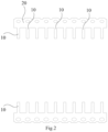
Fig. 2 is a schematic diagram of two rows of metal sheet as mentioned in operation S1 ofFig. 1 . -
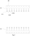
Fig.3 is a schematic diagram of two rows of metal sheet as mentioned in operation S2 ofFig. 1 with a clamping portion manufactured. -
Fig. 4 is a schematic diagram showing the operation S2 inFig. 1 , with brackets being fixed between the two rows of metal sheet. -
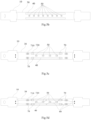
Figs. 5a to 5d are schematic diagrams showing the operation S3 inFig. 1 , with the bracket being prefabricated with conducting strip and attached with LED chips and rectifier module; one of the brackets is taken as an example here. -
Fig. 6 is a schematic diagram showing the operation S3 according to another embodiment, with the bracket being attached with LED chips, and the LED chips being electrically connected with the metal sheets by conducting wire; one of the brackets is taken as an example here. -
Fig. 7 is a schematic diagram showing the operation S4 inFig. 1 , with the bracket, all kinds of elements attached on the bracket, and the joints of the bracket and the metal sheets being packaged using packaging material. - The technical solutions of the embodiments of the present disclosure will be clearly and completely described in the following with reference to the accompanying drawings.
- It is understood that, reference to "embodiment" herein means that a particular feature, structure, or characteristic described may be included in at least one embodiment of the disclosure. The appearances of "embodiment" in various places in the specification are not necessarily all referring to the same embodiment, nor are they independent or alternative embodiments that are mutually exclusive with other embodiments. It is clearly and implicitly understood by those skilled in the art that the embodiments described herein may be combined with other embodiments.
- Please referring to
Figs. 1 to 6 , the method for manufacturing an LED filament according to the present disclosure includes the following operations. - Operation S1, a plurality of metal sheets are provided and arranged at least two rows in parallel, each
metal sheet 10 at one row has one end extending to the corresponding metal sheet at the other row, and the other ends of each of the metal sheets connect with each other to form a positioning portion. - Specifically, please referring to
Fig. 2 , in one embodiment, two rows ofmetal sheet 10 are prepared. Themetal sheet 10 may be made of metal with good conductive properties. Themetal sheet 10 may be obtained by dividing metal strips made in rolls into reasonable length, such as 120 millimeters or 144 millimeters. The two rows ofmetal sheet 10 may also be obtained by stamping an integral metal piece. - The two rows of
metal sheet 10 are arranged in parallel and spaced apart from each other, and each of themetal sheets 10 in a same row is aligned with each other. - Each
metal sheet 10 at one row has one end extending to thecorresponding metal sheet 10 at the other row, and the other ends of the eachmetal sheet 10 connects with each other to form apositioning portion 20. Thepositioning portion 20 is further defined with a plurality of positioning throughholes 210. - In some embodiments, the metal strips may be divided into thirty-six or forty or forty-eight
metal sheets 10 arranged in parallel and spaced apart from each other, the interval between every twoadjacent metal sheets 10 is equal, and the interval may be 1 millimeter to 9 millimeters. - Operation S2, a plurality of brackets are provided, and each bracket is located between two corresponding metal sheets and fixedly connected to the two metal sheets.
- Specifically, referring to
Fig. 4 , a plurality ofbrackets 30 are prepared, eachbracket 30 is fixedly connected with twometal sheets 10, and the twometal sheets 10 are located in different rows and facing to each other. As such, each twocorresponding metal sheets 10 are connected by abracket 30. - In some embodiments, the
bracket 30 may be obtained by dividing a bracket assembly, which includes a plurality of brackets connected in parallel side by side. The bracket assembly may include thirty-six or forty or forty-eight brackets, and is made of ceramic or glass. Each of thebrackets 30 may have a same width, such as 0.8 millimeters, 1.0 millimeter, 1.5 millimeters, or 3.0 millimeters. It should be understood that, the width of each of thebracket 30 may not be the same, and may be set according to an actual need. - In the invention, referring to
Figs. 3 and4 , in the operation S2, one end of each of themetal sheets 10 is defined with aclamping portion 110 for clamping thebracket 30. Specifically, theclamping portion 110 includes a pair ofclamping pieces clamping pieces cavity 1101 with themetal sheet 10, so that the end of thebracket 30 can be received in thereceiving cavity 1101. It can be understood that, theclamping portion 110 can also be integrally formed with themetal sheet 10 in operation S1. - In some embodiments, there is a one-to-one correspondence between the plurality of positioning through
holes 210 and thebrackets 30, so as to facilitate the positioning of thebrackets 30 when being connected to themetal sheets 10. - In some embodiments, referring to
Figs. 4 and5a , each of themetal sheets 10 is further defined with a markinghole 120. The markinghole 120 is configured to identify the positive pole and negative pole of themetal sheet 10, for instance, themetal sheet 10 having the markinghole 120 is set as a positive pole, and themetal sheet 10 without the markinghole 120 is set as a negative pole, or vice versa. The markinghole 120 may facilitate the identification of the positive pole and the negative pole in a subsequent process of solid-state wire bonding. It should be understood that the markinghole 120 may also be integrally formed with themetal sheet 10 in operation S1. - Operation S3, a plurality of LED chips are provided and attached to each of the brackets, and the LED chips are electrically connected to the metal sheets by conducting wire; or, each bracket is prefabricated with conducting strip, and the LED chips are attached to the bracket and electrically connected to the metal sheets by the conducting strip.
- Specifically, referring to
Figs. 5a-5d , in one embodiment, one of thebrackets 30 is taken as an example. Thebracket 30 is printed with two conductingstrips 40 at two sides of thebracket 30. Then, a set number ofLED chips 50 are sequentially attached to thebracket 30 and positioned between the two conducting strips 40. Finally, each of the conducting strips 40 is electrically connected to themetal sheets 10 located near to its both ends by welding lead, and the LED chips 50 are electrically connected to the conducting strips 40 via conducting wires. - The LED chips 50 may be high-voltage chips or low-voltage chips, which is not limited in the present disclosure.
- Each
bracket 30 is attached with arectifier module 70, which is positioned at an end of thebracket 30 closing to themetal sheet 10. - The
rectifier module 70 may specifically include arectifier bridge 710 and aprotective resistor 720. Therectifier bridge 710 may be consisted of four high-voltage LED chips with different conduction directions, so as to be able to convert external AC power to DC power to enable the LED chips 50. Theprotective resistor 720 is configured for stabilizing the current and voltage when the LED filament is forwarded and reversely cut-off, so as to effectively avoid the AC LED filament from breakdown due to overcurrent and overvoltage during work. In other embodiments, therectifier module 70 may include only therectifier bridge 710, which is not limited in the present disclosure. - It should be understood that, by arranging the
rectifier module 70 on thebracket 30, the LED filament that is finally manufactured can be directly connected to an AC power, which takes a lower cost than that of the conventional DC filament, and the power supply adopted for the LED filament may also be a lowcost power supply. Further, the stability of the AC LED filament is effectively improved, and the occurrence of die modulation phenomenon which may be caused by the instability of a crude power supply's filtering and voltage reduction is reduced. In addition, the method for manufacturing the AC LED filament does not need many of the components as used in many power supply solutions, such as expensive rectifiers and capacitors, thereby further reducing the cost. - Please referring to
Fig. 6 , according to another embodiment of the present disclosure, a set number ofLED chips 50, such as eight or tenLED chips 50, are sequentially arranged and fixed to thebracket 30 and electrically connected with each other through aconducting wire 60, and the LED chips 50 are then electrically connected to thecorresponding metal sheets 10 by theconducting wire 60. - Optionally, the quantity of the LED chips 50 attached to the
bracket 30 may be set according to actual requirement. Other logical circuits can also be set by setting reasonable bonding positions and wire bonding methods. It is not limited in the present disclosure. - Operation S4, referring to
Fig. 7 , each bracket, the LED chips defined on the bracket, the conducting strip or the conducting wire defined on the bracket, and the joints of the bracket and the metal sheets are all cladded using packaging material to form anencapsulation layer 80, and theencapsulation layer 80, thebracket 30, the LED chips 50, the conductingstrip 40 and/ or conductingwires 60, and the connected twometal sheets 10 cooperatively form an LED filament. - Specifically, referring to
Figs. 5a-5d ,6 and 7 , in one embodiment, after the LED chips 50 being attached to thebracket 30 and electrically connected to themetal sheets 10 by conductingstrip 40 and/or conductingwire 60, packaging material is used to package thebracket 30, the LED chips 50 and conducting strip 40 (and/or conducting wire 60), and the joints of thebracket 30 and themetal sheets 10 to form anencapsulation layer 80. Theencapsulation layer 80, thebracket 30, the LED chips 50, the conductingstrip 40 or conductingwire 60, and the connected twometal sheets 10 cooperatively form the final LED filament. Specifically, the clampingportion 110 is also cladded by theencapsulation layer 80. - The
packaging layer 80 may completely isolate the LED chips 50 and thebracket 30 from air, so that oxidation of the LED chips 50 and thebracket 30 may be avoided, and a good environment is provided for the LED chips 50 to run well in a confined space. As such, the using life of the LED filament is also greatly improved. Theencapsulation layer 80 also wraps the joints of themetal sheets 10 and thebracket 30, which may reduce the possibility of the joints from being broken due to external influences, thereby the using life of the LED filament is further improved. - The packaging material used for the
packaging layer 80 may be one or more selected from a group consisting of silicone, rubber, resin, and fluorescent powder. It is not limited in the present disclosure. - In some embodiment, the method for manufacturing LED filament further includes operation S5 subsequent to the operation S4.
- Operation S5, the
metal sheet 10 is cut off at a position located between the positioningportion 20 and the joint of the bracket and the metal sheet to obtain separate LED filaments. The joint relates to the clampingportion 110 for clamping thebracket 30. - Specifically, the
metal sheet 10 is cut off at each of the positions located between the positioningportion 20 and the joint of thebracket 30 and themetal sheet 10, to obtain a plurality of separate LED filaments. - More specifically, the
metal sheet 10 is cut off at each of the positions between the markinghole 120 and the positioning throughhole 210, to obtain a plurality of LED filaments for separately using. - Compared to the related art, the method for manufacturing LED filament in the present disclosure can produce LED filament groups in batches, which simples the process and reduces the cost. Further, the encapsulation layer may completely isolate the LED chips and the brackets from air, so that oxidation of the LED chips and the brackets may be avoided, and a good environment is provided for the LED chips to run well in a confined space. As such, the using life of the LED filament is also greatly improved.
- It is to be understood, however, that even though numerous characteristics and advantages of the present exemplary embodiment have been set forth in the foregoing description, together with details of the structures and functions of the embodiment, the disclosure is illustrative only, and changes may be made in detail, especially in matters of shape, size, and arrangement of parts within the principles of the disclosure to the full extent indicated by the broad general meaning of the terms. The scope of the invention is however only as defined by the appended claims.
Claims (9)
- A method for manufacturing an LED filament, comprising:operation S1, providing a plurality of metal sheets (10) arranged in two rows in parallel, each metal sheet (10) at one row having one end extending to the corresponding metal sheet at the other row, and the other ends of the metal sheets (10) at said one row connecting with each other to form a positioning portion (20);operation S2, providing a plurality of brackets (30), and each bracket (30) being located between two corresponding metal sheets (10) and fixedly connected to the two metal sheets (10), the two corresponding metal sheets (10) being located in different rows and facing to each other, each of the metal sheets (10) defining a clamping part (110) for clamping the bracket (30);operation S3, providing a plurality of LED chips (50) and attaching the LED chips (50) to each of the brackets (30), and the LED chips (50) being electrically connected to the metal sheets (10) by conducting wire (60);operation S4, packaging each bracket (30), the LED chips (50) defined on the bracket (30), the conducting strip (40) or the conducting wire (60) defined on the bracket (30), and the joint of the bracket (30) and the metal sheet (10) using packaging material to form an encapsulation layer (80);the encapsulation layer (80), the bracket (30), the LED chips (50), the conducting strip (40) and/or conducting wire (60), and the connected two metal sheets (10) cooperatively forming the LED filament; andeach of the brackets (30) being attached with a rectifier module (70), andthe rectifier module (70) being defined at an end of the bracket (30) closing to the metal sheet (10).
- The method according to claim 1, further comprising:
operation S5, cutting off the metal sheet (10) at a position located between the positioning portion (20) and the joint of the bracket (30) and the metal sheet (10) to obtain a separate LED filament. - The method according to claim 2, wherein the positioning portion (20) is defined with a plurality of positioning through holes (210).
- The method according to claim 3, wherein the plurality of positioning through holes (210) are corresponding to each of the brackets (30).
- The method according to claim 1, wherein the clamping part (110) comprises a pair of clamping pieces (111, 112) facing and spaced from each other, the pair of clamping pieces (111, 112) are respectively bent and extended from opposite two sides of the metal sheet (10), the pair of clamping pieces (111, 112) and the metal sheet (10) cooperatively form a receiving cavity, and the end of the bracket (30) is received in the receiving cavity.
- The method according to claim 2, wherein each of the metal sheets (10) in one row is defined with a marking hole (120).
- The method according to claim 6, wherein in operation S5, the metal sheet (10) is cut off at the position located between the positioning through hole (210) and the marking hole (120) to obtain the LED filament.
- The method according to claim 1, wherein the packaging material comprises silicone, rubber, or resin.
- The method according to claim 1, wherein the bracket (30) is made of ceramic or glass.
Applications Claiming Priority (1)
| Application Number | Priority Date | Filing Date | Title |
|---|---|---|---|
| CN201911241236.3A CN111883636A (en) | 2019-12-06 | 2019-12-06 | Manufacturing method of LED lamp filament |
Publications (3)
| Publication Number | Publication Date |
|---|---|
| EP3832191A1 EP3832191A1 (en) | 2021-06-09 |
| EP3832191C0 EP3832191C0 (en) | 2024-10-02 |
| EP3832191B1 true EP3832191B1 (en) | 2024-10-02 |
Family
ID=69159634
Family Applications (1)
| Application Number | Title | Priority Date | Filing Date |
|---|---|---|---|
| EP20151385.0A Active EP3832191B1 (en) | 2019-12-06 | 2020-01-13 | Method for manufacturing light emitting diode filament |
Country Status (4)
| Country | Link |
|---|---|
| US (1) | US11199298B2 (en) |
| EP (1) | EP3832191B1 (en) |
| CN (1) | CN111883636A (en) |
| WO (1) | WO2021109321A1 (en) |
Families Citing this family (2)
| Publication number | Priority date | Publication date | Assignee | Title |
|---|---|---|---|---|
| CN115654387B (en) * | 2021-07-09 | 2025-11-21 | 东莞市一成照明科技有限公司 | LED filament and one-lamp double-color LED bulb convenient for automatic production |
| US12176473B1 (en) * | 2024-04-11 | 2024-12-24 | Peng Wang | LED packaging structure |
Family Cites Families (33)
| Publication number | Priority date | Publication date | Assignee | Title |
|---|---|---|---|---|
| US10473271B2 (en) * | 2015-08-17 | 2019-11-12 | Zhejiang Super Lighting Electric Appliance Co., Ltd. | LED filament module and LED light bulb |
| US8905610B2 (en) * | 2009-01-26 | 2014-12-09 | Flex Lighting Ii, Llc | Light emitting device comprising a lightguide film |
| EP2817559A1 (en) * | 2012-02-21 | 2014-12-31 | Zeta Specialist Lighting Limited | Electric lamps and methods of manufacture of electrical devices |
| CN203026552U (en) * | 2012-12-06 | 2013-06-26 | 上海顿格电子贸易有限公司 | LED (lighting emitted diode) component bracket |
| CN103388805B (en) * | 2013-07-01 | 2015-03-18 | 临安市新三联照明电器有限公司 | LED (Light Emitting Diode) filament support series connection forming method based on support material plate |
| CN203553212U (en) * | 2013-11-29 | 2014-04-16 | 惠州市英吉尔光电科技有限公司 | Composable wafer direct packaging COB support |
| CN204257706U (en) * | 2014-10-29 | 2015-04-08 | 王文娟 | A kind of LED light source encapsulating structure |
| CN204289440U (en) * | 2014-12-12 | 2015-04-22 | 陈广明 | Novel LED filament five metals support |
| CN204348760U (en) * | 2014-12-19 | 2015-05-20 | 苏州天微工业技术有限公司 | LED silk |
| CN104600181A (en) * | 2015-01-29 | 2015-05-06 | 江西合晶科技有限公司 | LED (Light Emitting Diode) light bar and preparation method thereof |
| TWI651491B (en) * | 2015-07-23 | 2019-02-21 | 晶元光電股份有限公司 | Illuminating device |
| CN205177876U (en) * | 2015-12-02 | 2016-04-20 | 杭州恒星高虹光电科技股份有限公司 | AC flexible LED filament that gives off light |
| CN205118739U (en) * | 2015-12-03 | 2016-03-30 | 陈广明 | Ceramic strip filament structure |
| CN105387355A (en) * | 2015-12-10 | 2016-03-09 | 山东晶泰星光电科技有限公司 | Parallel-connection type light emitting diode (LED) illuminants and LED illuminating lamp |
| CN205564814U (en) * | 2016-03-22 | 2016-09-07 | 深圳市朗煜光电科技有限公司 | Led lamp filament structure |
| CN205657082U (en) * | 2016-04-11 | 2016-10-19 | 江西省木林森光电科技有限公司 | LED base plate material area |
| CN205592683U (en) * | 2016-04-12 | 2016-09-21 | 浙江阳光美加照明有限公司 | Luminous rim of LED and use LED ball bubble lamp of luminous rim of this LED |
| TW201705557A (en) * | 2016-10-26 | 2017-02-01 | 液光固態照明股份有限公司 | LED filament with heat dissipation structure and LED bulb using the same |
| CN206682890U (en) * | 2017-04-24 | 2017-11-28 | 深圳市源磊科技有限公司 | Filament support, LED filament, filament support plate and LED filament plate |
| DE102017110378B4 (en) * | 2017-05-12 | 2023-03-02 | Ledvance Gmbh | LED lamp with LED bulbs |
| CN107477381A (en) * | 2017-09-18 | 2017-12-15 | 叶逢新 | LED circuit board and LED support |
| TWI661550B (en) * | 2017-10-18 | 2019-06-01 | Yi Jhen Lee | Flexible light emitting diode (led) filament and the combination thereof |
| DE102017127721A1 (en) * | 2017-11-23 | 2019-05-23 | Osram Opto Semiconductors Gmbh | LED FILAMENT WITH CONVERSION LAYER |
| CN207729532U (en) * | 2018-01-08 | 2018-08-14 | 昆山市品能精密电子有限公司 | LED filament supporting structure |
| CN208189621U (en) * | 2018-03-23 | 2018-12-04 | 龙岩德煜照明有限公司 | A kind of LED support polarity identification structure |
| CN208014703U (en) * | 2018-03-29 | 2018-10-26 | 昆山工研院新型平板显示技术中心有限公司 | Drive backboard, micro- LED display panel and display |
| US10234079B1 (en) * | 2018-05-07 | 2019-03-19 | Ledvance Llc | Self-supporting filament light emitting diode light engine lamp assembly |
| CN108511432A (en) * | 2018-05-18 | 2018-09-07 | 梁倩 | LED support and packaging |
| CN208889654U (en) * | 2018-10-12 | 2019-05-21 | 深圳市欣上科技有限公司 | Without substrate filament framework, without substrate flexibility filament and light source |
| CN209045607U (en) * | 2018-11-06 | 2019-06-28 | 浙江英特来光电科技有限公司 | A LED-G9 Filament Holder |
| CN209309918U (en) * | 2018-11-13 | 2019-08-27 | 中山市木林森电子有限公司 | The LED support and LED light source of a plurality of light bar can be set |
| CN110345405B (en) * | 2019-08-09 | 2021-08-10 | 厦门多彩光电子科技有限公司 | Exchange flexible filament of COB and lamps and lanterns |
| CN110416397A (en) * | 2019-08-23 | 2019-11-05 | 中山市木林森电子有限公司 | The LED filament bracket of random length and the manufacturing process of LED filament can be done |
-
2019
- 2019-12-06 CN CN201911241236.3A patent/CN111883636A/en active Pending
-
2020
- 2020-01-10 WO PCT/CN2020/071349 patent/WO2021109321A1/en not_active Ceased
- 2020-01-13 EP EP20151385.0A patent/EP3832191B1/en active Active
- 2020-01-15 US US16/744,112 patent/US11199298B2/en active Active
Also Published As
| Publication number | Publication date |
|---|---|
| EP3832191A1 (en) | 2021-06-09 |
| WO2021109321A1 (en) | 2021-06-10 |
| EP3832191C0 (en) | 2024-10-02 |
| CN111883636A (en) | 2020-11-03 |
| US11199298B2 (en) | 2021-12-14 |
| US20210172573A1 (en) | 2021-06-10 |
Similar Documents
| Publication | Publication Date | Title |
|---|---|---|
| US9653668B2 (en) | LED filament and filament-type LED bulb | |
| CN106206761B (en) | Solar cell chip arrays, solar cell module and preparation method thereof | |
| US11199298B2 (en) | Method for manufacturing light emitting diode filament | |
| CN217655878U (en) | LED lamp bead and LED lamp strip | |
| CN103682018B (en) | Light-emitting diode and manufacturing method thereof | |
| CN214898436U (en) | Multi-base-island lead frame chip packaging structure and power module driving circuit | |
| CN103682066B (en) | Light emitting diode module and manufacture method thereof | |
| CN103682019B (en) | Light-emitting diode and manufacturing method thereof | |
| CN216769135U (en) | LED lamp strip | |
| CN107830430B (en) | Substrate of LED lamp strip and LED lamp strip | |
| CN109630913B (en) | Method for manufacturing light emitting device | |
| CN212617756U (en) | LED paster flexible line lamp of series-parallel structure | |
| CN206312893U (en) | The packaging system of chopper circuit | |
| CN212064428U (en) | Lamp strip | |
| CN217655877U (en) | LED lamp bead and LED lamp strip | |
| CN207179284U (en) | LED blank | |
| CN221708700U (en) | Inverted constant-current tube element | |
| CN215731776U (en) | COB light source | |
| CN210136890U (en) | Single crystal and polycrystal sharing type lead frame and light emitting device thereof | |
| CN111489870B (en) | High-power high-resistance special-shaped cement resistor | |
| CN223610019U (en) | Lamp string group | |
| CN218677187U (en) | Support is used in LED production | |
| CN213656390U (en) | Flexible filament band capable of being made into any length | |
| CN215342590U (en) | UV lamp pearl support | |
| CN223306869U (en) | Novel LED lamp strip structure |
Legal Events
| Date | Code | Title | Description |
|---|---|---|---|
| PUAI | Public reference made under article 153(3) epc to a published international application that has entered the european phase |
Free format text: ORIGINAL CODE: 0009012 |
|
| STAA | Information on the status of an ep patent application or granted ep patent |
Free format text: STATUS: THE APPLICATION HAS BEEN PUBLISHED |
|
| AK | Designated contracting states |
Kind code of ref document: A1 Designated state(s): AL AT BE BG CH CY CZ DE DK EE ES FI FR GB GR HR HU IE IS IT LI LT LU LV MC MK MT NL NO PL PT RO RS SE SI SK SM TR |
|
| STAA | Information on the status of an ep patent application or granted ep patent |
Free format text: STATUS: REQUEST FOR EXAMINATION WAS MADE |
|
| 17P | Request for examination filed |
Effective date: 20211124 |
|
| RBV | Designated contracting states (corrected) |
Designated state(s): AL AT BE BG CH CY CZ DE DK EE ES FI FR GB GR HR HU IE IS IT LI LT LU LV MC MK MT NL NO PL PT RO RS SE SI SK SM TR |
|
| STAA | Information on the status of an ep patent application or granted ep patent |
Free format text: STATUS: EXAMINATION IS IN PROGRESS |
|
| 17Q | First examination report despatched |
Effective date: 20240104 |
|
| GRAP | Despatch of communication of intention to grant a patent |
Free format text: ORIGINAL CODE: EPIDOSNIGR1 |
|
| STAA | Information on the status of an ep patent application or granted ep patent |
Free format text: STATUS: GRANT OF PATENT IS INTENDED |
|
| INTG | Intention to grant announced |
Effective date: 20240529 |
|
| GRAS | Grant fee paid |
Free format text: ORIGINAL CODE: EPIDOSNIGR3 |
|
| GRAA | (expected) grant |
Free format text: ORIGINAL CODE: 0009210 |
|
| STAA | Information on the status of an ep patent application or granted ep patent |
Free format text: STATUS: THE PATENT HAS BEEN GRANTED |
|
| AK | Designated contracting states |
Kind code of ref document: B1 Designated state(s): AL AT BE BG CH CY CZ DE DK EE ES FI FR GB GR HR HU IE IS IT LI LT LU LV MC MK MT NL NO PL PT RO RS SE SI SK SM TR |
|
| REG | Reference to a national code |
Ref country code: GB Ref legal event code: FG4D |
|
| REG | Reference to a national code |
Ref country code: CH Ref legal event code: EP |
|
| REG | Reference to a national code |
Ref country code: DE Ref legal event code: R096 Ref document number: 602020038553 Country of ref document: DE |
|
| REG | Reference to a national code |
Ref country code: IE Ref legal event code: FG4D |
|
| U01 | Request for unitary effect filed |
Effective date: 20241022 |
|
| U07 | Unitary effect registered |
Designated state(s): AT BE BG DE DK EE FI FR IT LT LU LV MT NL PT RO SE SI Effective date: 20241105 |
|
| U20 | Renewal fee for the european patent with unitary effect paid |
Year of fee payment: 6 Effective date: 20250127 |
|
| PG25 | Lapsed in a contracting state [announced via postgrant information from national office to epo] |
Ref country code: HR Free format text: LAPSE BECAUSE OF FAILURE TO SUBMIT A TRANSLATION OF THE DESCRIPTION OR TO PAY THE FEE WITHIN THE PRESCRIBED TIME-LIMIT Effective date: 20241002 Ref country code: IS Free format text: LAPSE BECAUSE OF FAILURE TO SUBMIT A TRANSLATION OF THE DESCRIPTION OR TO PAY THE FEE WITHIN THE PRESCRIBED TIME-LIMIT Effective date: 20250202 |
|
| PG25 | Lapsed in a contracting state [announced via postgrant information from national office to epo] |
Ref country code: ES Free format text: LAPSE BECAUSE OF FAILURE TO SUBMIT A TRANSLATION OF THE DESCRIPTION OR TO PAY THE FEE WITHIN THE PRESCRIBED TIME-LIMIT Effective date: 20241002 |
|
| PG25 | Lapsed in a contracting state [announced via postgrant information from national office to epo] |
Ref country code: NO Free format text: LAPSE BECAUSE OF FAILURE TO SUBMIT A TRANSLATION OF THE DESCRIPTION OR TO PAY THE FEE WITHIN THE PRESCRIBED TIME-LIMIT Effective date: 20250102 |
|
| PG25 | Lapsed in a contracting state [announced via postgrant information from national office to epo] |
Ref country code: GR Free format text: LAPSE BECAUSE OF FAILURE TO SUBMIT A TRANSLATION OF THE DESCRIPTION OR TO PAY THE FEE WITHIN THE PRESCRIBED TIME-LIMIT Effective date: 20250103 |
|
| PG25 | Lapsed in a contracting state [announced via postgrant information from national office to epo] |
Ref country code: CZ Free format text: LAPSE BECAUSE OF FAILURE TO SUBMIT A TRANSLATION OF THE DESCRIPTION OR TO PAY THE FEE WITHIN THE PRESCRIBED TIME-LIMIT Effective date: 20241002 Ref country code: PL Free format text: LAPSE BECAUSE OF FAILURE TO SUBMIT A TRANSLATION OF THE DESCRIPTION OR TO PAY THE FEE WITHIN THE PRESCRIBED TIME-LIMIT Effective date: 20241002 |
|
| PG25 | Lapsed in a contracting state [announced via postgrant information from national office to epo] |
Ref country code: RS Free format text: LAPSE BECAUSE OF FAILURE TO SUBMIT A TRANSLATION OF THE DESCRIPTION OR TO PAY THE FEE WITHIN THE PRESCRIBED TIME-LIMIT Effective date: 20250102 |
|
| PG25 | Lapsed in a contracting state [announced via postgrant information from national office to epo] |
Ref country code: SM Free format text: LAPSE BECAUSE OF FAILURE TO SUBMIT A TRANSLATION OF THE DESCRIPTION OR TO PAY THE FEE WITHIN THE PRESCRIBED TIME-LIMIT Effective date: 20241002 |
|
| PG25 | Lapsed in a contracting state [announced via postgrant information from national office to epo] |
Ref country code: SK Free format text: LAPSE BECAUSE OF FAILURE TO SUBMIT A TRANSLATION OF THE DESCRIPTION OR TO PAY THE FEE WITHIN THE PRESCRIBED TIME-LIMIT Effective date: 20241002 |
|
| PLBE | No opposition filed within time limit |
Free format text: ORIGINAL CODE: 0009261 |
|
| STAA | Information on the status of an ep patent application or granted ep patent |
Free format text: STATUS: NO OPPOSITION FILED WITHIN TIME LIMIT |
|
| REG | Reference to a national code |
Ref country code: CH Ref legal event code: PL |
|
| 26N | No opposition filed |
Effective date: 20250703 |
|
| PG25 | Lapsed in a contracting state [announced via postgrant information from national office to epo] |
Ref country code: MC Free format text: LAPSE BECAUSE OF FAILURE TO SUBMIT A TRANSLATION OF THE DESCRIPTION OR TO PAY THE FEE WITHIN THE PRESCRIBED TIME-LIMIT Effective date: 20241002 |
|
| GBPC | Gb: european patent ceased through non-payment of renewal fee |
Effective date: 20250113 |
|
| PG25 | Lapsed in a contracting state [announced via postgrant information from national office to epo] |
Ref country code: GB Free format text: LAPSE BECAUSE OF NON-PAYMENT OF DUE FEES Effective date: 20250113 |
|
| PG25 | Lapsed in a contracting state [announced via postgrant information from national office to epo] |
Ref country code: CH Free format text: LAPSE BECAUSE OF NON-PAYMENT OF DUE FEES Effective date: 20250131 |
|
| U1N | Appointed representative for the unitary patent procedure changed after the registration of the unitary effect |
Representative=s name: HERRERO & ASOCIADOS, S.L.; ES |
|
| PG25 | Lapsed in a contracting state [announced via postgrant information from national office to epo] |
Ref country code: IE Free format text: LAPSE BECAUSE OF NON-PAYMENT OF DUE FEES Effective date: 20250113 |
|
| U20 | Renewal fee for the european patent with unitary effect paid |
Year of fee payment: 7 Effective date: 20260116 |