EP3832191B1 - Verfahren zur herstellung eines leuchtdiodenfilaments - Google Patents
Verfahren zur herstellung eines leuchtdiodenfilaments Download PDFInfo
- Publication number
- EP3832191B1 EP3832191B1 EP20151385.0A EP20151385A EP3832191B1 EP 3832191 B1 EP3832191 B1 EP 3832191B1 EP 20151385 A EP20151385 A EP 20151385A EP 3832191 B1 EP3832191 B1 EP 3832191B1
- Authority
- EP
- European Patent Office
- Prior art keywords
- bracket
- metal sheet
- metal sheets
- led chips
- led
- Prior art date
- Legal status (The legal status is an assumption and is not a legal conclusion. Google has not performed a legal analysis and makes no representation as to the accuracy of the status listed.)
- Active
Links
Images




Classifications
-
- F—MECHANICAL ENGINEERING; LIGHTING; HEATING; WEAPONS; BLASTING
- F21—LIGHTING
- F21K—NON-ELECTRIC LIGHT SOURCES USING LUMINESCENCE; LIGHT SOURCES USING ELECTROCHEMILUMINESCENCE; LIGHT SOURCES USING CHARGES OF COMBUSTIBLE MATERIAL; LIGHT SOURCES USING SEMICONDUCTOR DEVICES AS LIGHT-GENERATING ELEMENTS; LIGHT SOURCES NOT OTHERWISE PROVIDED FOR
- F21K9/00—Light sources using semiconductor devices as light-generating elements, e.g. using light-emitting diodes [LED] or lasers
- F21K9/90—Methods of manufacture
-
- H—ELECTRICITY
- H10—SEMICONDUCTOR DEVICES; ELECTRIC SOLID-STATE DEVICES NOT OTHERWISE PROVIDED FOR
- H10H—INORGANIC LIGHT-EMITTING SEMICONDUCTOR DEVICES HAVING POTENTIAL BARRIERS
- H10H20/00—Individual inorganic light-emitting semiconductor devices having potential barriers, e.g. light-emitting diodes [LED]
- H10H20/80—Constructional details
- H10H20/85—Packages
- H10H20/852—Encapsulations
-
- H—ELECTRICITY
- H10—SEMICONDUCTOR DEVICES; ELECTRIC SOLID-STATE DEVICES NOT OTHERWISE PROVIDED FOR
- H10H—INORGANIC LIGHT-EMITTING SEMICONDUCTOR DEVICES HAVING POTENTIAL BARRIERS
- H10H20/00—Individual inorganic light-emitting semiconductor devices having potential barriers, e.g. light-emitting diodes [LED]
- H10H20/80—Constructional details
- H10H20/85—Packages
- H10H20/852—Encapsulations
- H10H20/854—Encapsulations characterised by their material, e.g. epoxy or silicone resins
-
- H—ELECTRICITY
- H10—SEMICONDUCTOR DEVICES; ELECTRIC SOLID-STATE DEVICES NOT OTHERWISE PROVIDED FOR
- H10H—INORGANIC LIGHT-EMITTING SEMICONDUCTOR DEVICES HAVING POTENTIAL BARRIERS
- H10H20/00—Individual inorganic light-emitting semiconductor devices having potential barriers, e.g. light-emitting diodes [LED]
- H10H20/80—Constructional details
- H10H20/85—Packages
- H10H20/857—Interconnections, e.g. lead-frames, bond wires or solder balls
-
- H—ELECTRICITY
- H10—SEMICONDUCTOR DEVICES; ELECTRIC SOLID-STATE DEVICES NOT OTHERWISE PROVIDED FOR
- H10W—GENERIC PACKAGES, INTERCONNECTIONS, CONNECTORS OR OTHER CONSTRUCTIONAL DETAILS OF DEVICES COVERED BY CLASS H10
- H10W90/00—Package configurations
-
- H—ELECTRICITY
- H10—SEMICONDUCTOR DEVICES; ELECTRIC SOLID-STATE DEVICES NOT OTHERWISE PROVIDED FOR
- H10H—INORGANIC LIGHT-EMITTING SEMICONDUCTOR DEVICES HAVING POTENTIAL BARRIERS
- H10H20/00—Individual inorganic light-emitting semiconductor devices having potential barriers, e.g. light-emitting diodes [LED]
- H10H20/01—Manufacture or treatment
- H10H20/036—Manufacture or treatment of packages
- H10H20/0362—Manufacture or treatment of packages of encapsulations
-
- H—ELECTRICITY
- H10—SEMICONDUCTOR DEVICES; ELECTRIC SOLID-STATE DEVICES NOT OTHERWISE PROVIDED FOR
- H10H—INORGANIC LIGHT-EMITTING SEMICONDUCTOR DEVICES HAVING POTENTIAL BARRIERS
- H10H20/00—Individual inorganic light-emitting semiconductor devices having potential barriers, e.g. light-emitting diodes [LED]
- H10H20/01—Manufacture or treatment
- H10H20/036—Manufacture or treatment of packages
- H10H20/0364—Manufacture or treatment of packages of interconnections
Definitions
- the present disclosure relates to the field of light emitting diode (LED) filament, and more particularly to a method for manufacturing LED filaments.
- LED light emitting diode
- LED street lamps are almost direct current (DC) droved, that is, a mature switching power supply technology is used to turn the alternating current (AC) into DC to drive the LED filament.
- DC direct current
- AC alternating current
- Related prior art to the manufacturing of related filaments can be found in CN104600181A , CN205592683 U , EP2846083A1 , and CN110345505 A .
- DC driving has become a mainstream driving method since it can provide stable current for LED.
- the development of DC driving may be restricted by the bottlenecks of using life and cost. Simultaneously, it is very complicated to manufacture a DC droved filament, which further raises the cost.
- the present disclosure is to provide a method for manufacturing light emitting diode filament, which aims to solve the problem of complicated manufacturing process and high cost for the filament.
- the present disclosure provides a method for manufacturing an LED filament, according to claim 1, and the method includes the following operations S1 to S4.
- Operation S1 a plurality of metal sheets are provided and arranged at least two rows in parallel, each metal sheet at one row has one end extending to the corresponding metal sheet at the other row, and the other ends of each of the metal sheets connect with each other to form a positioning portion;
- operation S2 a plurality of brackets are provided, and each bracket is located between two corresponding metal sheets and fixedly connected to the two metal sheets;
- operation S3, a plurality of LED chips are provided and attached to each of the brackets, and the LED chips are electrically connected to the metal sheets by conducting wire; or, each bracket is prefabricated with conducting strip, and the LED chips are attached to the bracket and electrically connected to the metal sheets by the conducting strip;
- each bracket, the LED chips defined on the bracket, the conducting strip or the conducting wire defined on the bracket, and the joints of the bracket and the metal sheets are all cladded using packaging material to form an
- the method for manufacturing LED filament further includes operation S5, which cuts off the metal sheet at a position located between the positioning portion and the joint of the bracket and the metal sheet to obtain separate LED filaments.
- the positioning portion is defined with a plurality of positioning through holes.
- the plurality of positioning through holes are corresponding to each of the brackets.
- each metal sheet defines a clamping part for clamping the bracket.
- the clamping part includes a pair of clamping pieces facing and spaced from each other, the pair of clamping pieces are respectively bent and extended from opposite two sides of the metal sheet, the pair of clamping pieces and the metal sheet cooperatively form a receiving cavity, and the end of the bracket is received in the receiving cavity.
- each of the metal sheets in one row is defined with a marking hole.
- the metal sheet is cut off at the position located between the positioning through hole and the marking hole to obtain the LED filament.
- each bracket is attached with a rectifier module, and the rectifier module is defined at an end of the bracket closing to the metal sheet.
- the packaging material includes silicone, rubber, or resin.
- the bracket is made of ceramic or glass.
- the method for manufacturing LED filament can produce LED filament groups in batches, which simples the manufacturing process and reduces the cost. Further, the encapsulation layer may completely isolate the LED chips and the brackets from air, so that oxidation of the LED chips and the brackets may be avoided, and a good environment is provided for the LED chips to run well in a confined space. As such, the using life of the LED filament is also greatly improved.
- the method for manufacturing an LED filament according to the present disclosure includes the following operations.
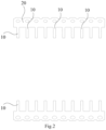
- each metal sheet 10 at one row has one end extending to the corresponding metal sheet at the other row, and the other ends of each of the metal sheets connect with each other to form a positioning portion.
- the metal sheet 10 may be made of metal with good conductive properties.
- the metal sheet 10 may be obtained by dividing metal strips made in rolls into reasonable length, such as 120 millimeters or 144 millimeters.
- the two rows of metal sheet 10 may also be obtained by stamping an integral metal piece.
- the two rows of metal sheet 10 are arranged in parallel and spaced apart from each other, and each of the metal sheets 10 in a same row is aligned with each other.
- Each metal sheet 10 at one row has one end extending to the corresponding metal sheet 10 at the other row, and the other ends of the each metal sheet 10 connects with each other to form a positioning portion 20.
- the positioning portion 20 is further defined with a plurality of positioning through holes 210.
- the metal strips may be divided into thirty-six or forty or forty-eight metal sheets 10 arranged in parallel and spaced apart from each other, the interval between every two adjacent metal sheets 10 is equal, and the interval may be 1 millimeter to 9 millimeters.
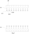
- each bracket is located between two corresponding metal sheets and fixedly connected to the two metal sheets.
- the bracket 30 may be obtained by dividing a bracket assembly, which includes a plurality of brackets connected in parallel side by side.
- the bracket assembly may include thirty-six or forty or forty-eight brackets, and is made of ceramic or glass.
- Each of the brackets 30 may have a same width, such as 0.8 millimeters, 1.0 millimeter, 1.5 millimeters, or 3.0 millimeters. It should be understood that, the width of each of the bracket 30 may not be the same, and may be set according to an actual need.
- the clamping portion 110 includes a pair of clamping pieces 111 and 112, and the clamping pieces 111 and 112 face to each other and are spaced apart from each other.
- the pair of clamping pieces are respectively bent and extended from opposite two sides of the metal sheet, and cooperatively define a receiving cavity 1101 with the metal sheet 10, so that the end of the bracket 30 can be received in the receiving cavity 1101.
- the clamping portion 110 can also be integrally formed with the metal sheet 10 in operation S1.
- each of the metal sheets 10 is further defined with a marking hole 120.
- the marking hole 120 is configured to identify the positive pole and negative pole of the metal sheet 10, for instance, the metal sheet 10 having the marking hole 120 is set as a positive pole, and the metal sheet 10 without the marking hole 120 is set as a negative pole, or vice versa.
- the marking hole 120 may facilitate the identification of the positive pole and the negative pole in a subsequent process of solid-state wire bonding. It should be understood that the marking hole 120 may also be integrally formed with the metal sheet 10 in operation S1.
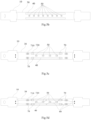
- one of the brackets 30 is taken as an example.
- the bracket 30 is printed with two conducting strips 40 at two sides of the bracket 30.
- a set number of LED chips 50 are sequentially attached to the bracket 30 and positioned between the two conducting strips 40.
- each of the conducting strips 40 is electrically connected to the metal sheets 10 located near to its both ends by welding lead, and the LED chips 50 are electrically connected to the conducting strips 40 via conducting wires.
- the LED chips 50 may be high-voltage chips or low-voltage chips, which is not limited in the present disclosure.
- Each bracket 30 is attached with a rectifier module 70, which is positioned at an end of the bracket 30 closing to the metal sheet 10.
- the rectifier module 70 may specifically include a rectifier bridge 710 and a protective resistor 720.
- the rectifier bridge 710 may be consisted of four high-voltage LED chips with different conduction directions, so as to be able to convert external AC power to DC power to enable the LED chips 50.
- the protective resistor 720 is configured for stabilizing the current and voltage when the LED filament is forwarded and reversely cut-off, so as to effectively avoid the AC LED filament from breakdown due to overcurrent and overvoltage during work.
- the rectifier module 70 may include only the rectifier bridge 710, which is not limited in the present disclosure.
- the LED filament that is finally manufactured can be directly connected to an AC power, which takes a lower cost than that of the conventional DC filament, and the power supply adopted for the LED filament may also be a lowcost power supply. Further, the stability of the AC LED filament is effectively improved, and the occurrence of die modulation phenomenon which may be caused by the instability of a crude power supply's filtering and voltage reduction is reduced. In addition, the method for manufacturing the AC LED filament does not need many of the components as used in many power supply solutions, such as expensive rectifiers and capacitors, thereby further reducing the cost.
- a set number of LED chips 50 such as eight or ten LED chips 50, are sequentially arranged and fixed to the bracket 30 and electrically connected with each other through a conducting wire 60, and the LED chips 50 are then electrically connected to the corresponding metal sheets 10 by the conducting wire 60.
- the quantity of the LED chips 50 attached to the bracket 30 may be set according to actual requirement.
- Other logical circuits can also be set by setting reasonable bonding positions and wire bonding methods. It is not limited in the present disclosure.
- each bracket, the LED chips defined on the bracket, the conducting strip or the conducting wire defined on the bracket, and the joints of the bracket and the metal sheets are all cladded using packaging material to form an encapsulation layer 80, and the encapsulation layer 80, the bracket 30, the LED chips 50, the conducting strip 40 and/ or conducting wires 60, and the connected two metal sheets 10 cooperatively form an LED filament.
- packaging material is used to package the bracket 30, the LED chips 50 and conducting strip 40 (and/or conducting wire 60), and the joints of the bracket 30 and the metal sheets 10 to form an encapsulation layer 80.
- the encapsulation layer 80, the bracket 30, the LED chips 50, the conducting strip 40 or conducting wire 60, and the connected two metal sheets 10 cooperatively form the final LED filament.
- the clamping portion 110 is also cladded by the encapsulation layer 80.
- the packaging layer 80 may completely isolate the LED chips 50 and the bracket 30 from air, so that oxidation of the LED chips 50 and the bracket 30 may be avoided, and a good environment is provided for the LED chips 50 to run well in a confined space. As such, the using life of the LED filament is also greatly improved.
- the encapsulation layer 80 also wraps the joints of the metal sheets 10 and the bracket 30, which may reduce the possibility of the joints from being broken due to external influences, thereby the using life of the LED filament is further improved.
- the method for manufacturing LED filament further includes operation S5 subsequent to the operation S4.
- the metal sheet 10 is cut off at a position located between the positioning portion 20 and the joint of the bracket and the metal sheet to obtain separate LED filaments.
- the joint relates to the clamping portion 110 for clamping the bracket 30.
- the metal sheet 10 is cut off at each of the positions located between the positioning portion 20 and the joint of the bracket 30 and the metal sheet 10, to obtain a plurality of separate LED filaments.
- the metal sheet 10 is cut off at each of the positions between the marking hole 120 and the positioning through hole 210, to obtain a plurality of LED filaments for separately using.
- the method for manufacturing LED filament in the present disclosure can produce LED filament groups in batches, which simples the process and reduces the cost. Further, the encapsulation layer may completely isolate the LED chips and the brackets from air, so that oxidation of the LED chips and the brackets may be avoided, and a good environment is provided for the LED chips to run well in a confined space. As such, the using life of the LED filament is also greatly improved.
Landscapes
- Engineering & Computer Science (AREA)
- Manufacturing & Machinery (AREA)
- Physics & Mathematics (AREA)
- Microelectronics & Electronic Packaging (AREA)
- Optics & Photonics (AREA)
- General Engineering & Computer Science (AREA)
- Led Device Packages (AREA)
Claims (9)
- Eine Methode für die Herstellung eines LED-Leuchtadens, die Folgendes umfasst:Arbeitsgang S1, bei der eine Vielzahl von Metallblättern (10), die in zwei parallelen Reihen angeordnet sind, vorgesehen ist, jedes Metallblatt (10) in einer Reihe mit einen Ende, das sich zum entsprechenden Metallblatt der anderen Reihe erstreckt, und wobei die anderen Enden des Metallblattes (10) in besgter einen Reihe untereinander verbunden sind, um einen Positionierteil (20) zu bilden;Arbeitsgang S2, Bereitstellung einer Vielszahl von Halterungenn (30), und wobei jede Halterung (30) zwischen zwei entsprechenden Metallblättern (10) lokalisiert ist und fest mit den beiden Metallblättern (10) verbunden ist, die beiden entsprechenden Metallblätter (10) in verschiedenen Reihen lokalisiert sind und einander gegenüber liegen, wobei jedes Metallblatt (10) einen Klemmteil (110) zum Einklemmen der Halterung (30) definiert ;Arbeitsgang S3, Bereitstellung einer Vielzahl von LED-Chips (50) und Befestigen der LED.Chips (50) an jede der Halterungen (30) und wobei die LED-Chips (50) elektrisch mit den Metallblättern (10) über einen leitenden Draht (60) verbunden ist;Arbeitsgang S4, Verkapseln jeder Halterung (30), des an der Halterung (30) definierten Leitbandes (40) oder Leitdrahts (60) und der Verbindungsstelle der Halterung (30) und des Metallblatts (10) unter Verwendung des Verkapselungsmaterials, um eine verkapselte Schicht (80) zu bilden, wobei die Verkapselungsschicht (80), die Halterung (30), die LED-Chips (50), das Leitband (40) und/oder Leitkabel (60) und die beiden verbundenen Metallblätter (10) in kooperativer Weise den LED-Leuchtfaden bilden; undWobei jede Halterung (30) an ein Gleichrichtermodul (70) angeschlossen ist und das Gleichrichtermodul (70) an einem Ende der Halterung (30) mit dem Metallblatt (10) anschliessend definiert ist.
- Die Methode gemäss Anspruch 1, die weiter Folgendes umfasst:
Arbeitsgang S5 Abschneiden des Metallblattes (10) en einer Position, die zwischen dem Positionierteil (20) und der Verbindungsstelle der Halterung (30) und dem Metallblatt (10) lokalisiert ist, um ein separates LED-Leuchtfaden zu erhalten. - Die Methode gemäss Anspruch 2, bei der der Positionierteil (20) mit einer Vielzahl von Positionierungsdurchgangslöchern (210) definiert ist.
- Die Methode gemäss Anspruch 3, bei der die Vielzahl von Positionierungsdurchgangslöchern (210) jeder der Halterungen (30) entsprechen.
- Die Methode gemäss Anspruch 1, bei der der Klemmteil (110) ein Paar Klemmstücke (111,112) umfasst, die einander zugewandt und beabstandet sind, wobei ein Paar Klemmstücke (111, 112) jeweils gebogen sind und sich von gegenüberliegenden zwei Seiten des Metallblattes (10) erstrecken, das Paar Klemmstücke (111,112) und das Metallblatt (10) kooperiernd eine Aufnahmevertiefung bilden und das Ende der Halterung (30) in der Aufnahmevertiefung aufgenommen wird.
- Die Methode gemäss Anspruch 2, bei der jedes Metallblatt (10) in einer Reihe mit einem Markierungsloch (120) definiert ist.
- Die Methode gemäss Anspruch 6, bei der in Arbeitsgang S5 das Metallblatt (10) in der zwischen dem Positionierungsdurchgangsloch (210) und dem Markierungsloch (120) lokalisierten Position abgeschnitten wird, um den LED-Leuchtfaden zu erhalten.
- Die Methode gemäss Anspruch 1, bei der das Verkapselungsmaterial Silikon, Kautschuk oder Harz enthält.
- Die Methode gemäss Anspruch 1, bei der die Halterung (30) aus Keramikmaterial oder Glas gefertigt ist.
Applications Claiming Priority (1)
| Application Number | Priority Date | Filing Date | Title |
|---|---|---|---|
| CN201911241236.3A CN111883636A (zh) | 2019-12-06 | 2019-12-06 | Led灯丝的制造方法 |
Publications (3)
| Publication Number | Publication Date |
|---|---|
| EP3832191A1 EP3832191A1 (de) | 2021-06-09 |
| EP3832191C0 EP3832191C0 (de) | 2024-10-02 |
| EP3832191B1 true EP3832191B1 (de) | 2024-10-02 |
Family
ID=69159634
Family Applications (1)
| Application Number | Title | Priority Date | Filing Date |
|---|---|---|---|
| EP20151385.0A Active EP3832191B1 (de) | 2019-12-06 | 2020-01-13 | Verfahren zur herstellung eines leuchtdiodenfilaments |
Country Status (4)
| Country | Link |
|---|---|
| US (1) | US11199298B2 (de) |
| EP (1) | EP3832191B1 (de) |
| CN (1) | CN111883636A (de) |
| WO (1) | WO2021109321A1 (de) |
Families Citing this family (2)
| Publication number | Priority date | Publication date | Assignee | Title |
|---|---|---|---|---|
| CN115654387B (zh) * | 2021-07-09 | 2025-11-21 | 东莞市一成照明科技有限公司 | 一种led灯丝及便于自动化生产的一灯双色led灯泡 |
| US12176473B1 (en) * | 2024-04-11 | 2024-12-24 | Peng Wang | LED packaging structure |
Family Cites Families (33)
| Publication number | Priority date | Publication date | Assignee | Title |
|---|---|---|---|---|
| US10473271B2 (en) * | 2015-08-17 | 2019-11-12 | Zhejiang Super Lighting Electric Appliance Co., Ltd. | LED filament module and LED light bulb |
| US8905610B2 (en) * | 2009-01-26 | 2014-12-09 | Flex Lighting Ii, Llc | Light emitting device comprising a lightguide film |
| EP2817559A1 (de) * | 2012-02-21 | 2014-12-31 | Zeta Specialist Lighting Limited | Elektrolampen und verfahren zur herstellung elektrischer vorrichtungen |
| CN203026552U (zh) * | 2012-12-06 | 2013-06-26 | 上海顿格电子贸易有限公司 | Led发光元器件支架 |
| CN103388805B (zh) * | 2013-07-01 | 2015-03-18 | 临安市新三联照明电器有限公司 | 一种基于支架料板的led灯丝支架成型方法 |
| CN203553212U (zh) * | 2013-11-29 | 2014-04-16 | 惠州市英吉尔光电科技有限公司 | 一种可组合的晶片直接封装cob支架 |
| CN204257706U (zh) * | 2014-10-29 | 2015-04-08 | 王文娟 | 一种led光源封装结构 |
| CN204289440U (zh) * | 2014-12-12 | 2015-04-22 | 陈广明 | 一种新型led灯丝五金支架 |
| CN204348760U (zh) * | 2014-12-19 | 2015-05-20 | 苏州天微工业技术有限公司 | Led灯丝 |
| CN104600181A (zh) * | 2015-01-29 | 2015-05-06 | 江西合晶科技有限公司 | 一种led灯条及其制备方法 |
| TWI651491B (zh) * | 2015-07-23 | 2019-02-21 | 晶元光電股份有限公司 | 發光裝置 |
| CN205177876U (zh) * | 2015-12-02 | 2016-04-20 | 杭州恒星高虹光电科技股份有限公司 | 一种ac可变形led发光灯丝 |
| CN205118739U (zh) * | 2015-12-03 | 2016-03-30 | 陈广明 | 一种陶瓷条灯丝结构 |
| CN105387355A (zh) * | 2015-12-10 | 2016-03-09 | 山东晶泰星光电科技有限公司 | 一种并联型led发光体及led照明灯 |
| CN205564814U (zh) * | 2016-03-22 | 2016-09-07 | 深圳市朗煜光电科技有限公司 | Led灯丝结构 |
| CN205657082U (zh) * | 2016-04-11 | 2016-10-19 | 江西省木林森光电科技有限公司 | 一种led基板料带 |
| CN205592683U (zh) * | 2016-04-12 | 2016-09-21 | 浙江阳光美加照明有限公司 | 一种led发光灯框及使用该led发光灯框的led球泡灯 |
| TW201705557A (zh) * | 2016-10-26 | 2017-02-01 | 液光固態照明股份有限公司 | 具有散熱結構的led燈絲及應用該led燈絲的led燈泡 |
| CN206682890U (zh) * | 2017-04-24 | 2017-11-28 | 深圳市源磊科技有限公司 | 灯丝支架、led灯丝、灯丝支架板和led灯丝板 |
| DE102017110378B4 (de) * | 2017-05-12 | 2023-03-02 | Ledvance Gmbh | LED-Lampe mit LED-Leuchtmittel |
| CN107477381A (zh) * | 2017-09-18 | 2017-12-15 | 叶逢新 | Led线路板及led支架 |
| TWI661550B (zh) * | 2017-10-18 | 2019-06-01 | Yi Jhen Lee | 可撓性發光二極體(led)燈絲及其組合 |
| DE102017127721A1 (de) * | 2017-11-23 | 2019-05-23 | Osram Opto Semiconductors Gmbh | Led-filament mit konversionsschicht |
| CN207729532U (zh) * | 2018-01-08 | 2018-08-14 | 昆山市品能精密电子有限公司 | Led灯丝支架结构 |
| CN208189621U (zh) * | 2018-03-23 | 2018-12-04 | 龙岩德煜照明有限公司 | 一种led支架极性识别结构 |
| CN208014703U (zh) * | 2018-03-29 | 2018-10-26 | 昆山工研院新型平板显示技术中心有限公司 | 驱动背板、微发光二极管显示面板及显示器 |
| US10234079B1 (en) * | 2018-05-07 | 2019-03-19 | Ledvance Llc | Self-supporting filament light emitting diode light engine lamp assembly |
| CN108511432A (zh) * | 2018-05-18 | 2018-09-07 | 梁倩 | Led支架及封装器件 |
| CN208889654U (zh) * | 2018-10-12 | 2019-05-21 | 深圳市欣上科技有限公司 | 无基材灯丝架构、无基材柔性灯丝及光源 |
| CN209045607U (zh) * | 2018-11-06 | 2019-06-28 | 浙江英特来光电科技有限公司 | 一种led-g9灯丝支架 |
| CN209309918U (zh) * | 2018-11-13 | 2019-08-27 | 中山市木林森电子有限公司 | 可设多条灯带的led支架及led光源 |
| CN110345405B (zh) * | 2019-08-09 | 2021-08-10 | 厦门多彩光电子科技有限公司 | 一种交流cob柔性灯丝及灯具 |
| CN110416397A (zh) * | 2019-08-23 | 2019-11-05 | 中山市木林森电子有限公司 | 可做任意长度的led灯丝支架及led灯丝的制造工艺 |
-
2019
- 2019-12-06 CN CN201911241236.3A patent/CN111883636A/zh active Pending
-
2020
- 2020-01-10 WO PCT/CN2020/071349 patent/WO2021109321A1/zh not_active Ceased
- 2020-01-13 EP EP20151385.0A patent/EP3832191B1/de active Active
- 2020-01-15 US US16/744,112 patent/US11199298B2/en active Active
Also Published As
| Publication number | Publication date |
|---|---|
| EP3832191A1 (de) | 2021-06-09 |
| WO2021109321A1 (zh) | 2021-06-10 |
| EP3832191C0 (de) | 2024-10-02 |
| CN111883636A (zh) | 2020-11-03 |
| US11199298B2 (en) | 2021-12-14 |
| US20210172573A1 (en) | 2021-06-10 |
Similar Documents
| Publication | Publication Date | Title |
|---|---|---|
| US9653668B2 (en) | LED filament and filament-type LED bulb | |
| CN106206761B (zh) | 太阳能电池片阵列、太阳能电池组件及其制备方法 | |
| US11199298B2 (en) | Method for manufacturing light emitting diode filament | |
| CN217655878U (zh) | Led灯珠及led灯带 | |
| CN103682018B (zh) | 发光二极管及其制造方法 | |
| CN214898436U (zh) | 一种多基岛引线框架芯片封装结构及电源模组驱动电路 | |
| CN103682066B (zh) | 发光二极管模组及其制造方法 | |
| CN103682019B (zh) | 发光二极管及其制造方法 | |
| CN216769135U (zh) | 一种led灯带 | |
| CN107830430B (zh) | 一种led灯条的基板及led灯条 | |
| CN109630913B (zh) | 发光装置的制造方法 | |
| CN212617756U (zh) | 一种并串联结构的led贴片软线灯 | |
| CN206312893U (zh) | 斩波电路的封装装置 | |
| CN212064428U (zh) | 一种灯条 | |
| CN217655877U (zh) | Led灯珠及led灯带 | |
| CN207179284U (zh) | Led灯带坯料 | |
| CN221708700U (zh) | 一种倒装恒流管元件 | |
| CN215731776U (zh) | Cob光源 | |
| CN210136890U (zh) | 单晶、多晶共享型导线架及其发光装置 | |
| CN111489870B (zh) | 一种大功率高阻异型水泥电阻器 | |
| CN223610019U (zh) | 灯带组 | |
| CN218677187U (zh) | 一种led生产用支架 | |
| CN213656390U (zh) | 一种可做任意长度的柔性灯丝带 | |
| CN215342590U (zh) | 一种uv灯珠支架 | |
| CN223306869U (zh) | 一种新型led灯带结构 |
Legal Events
| Date | Code | Title | Description |
|---|---|---|---|
| PUAI | Public reference made under article 153(3) epc to a published international application that has entered the european phase |
Free format text: ORIGINAL CODE: 0009012 |
|
| STAA | Information on the status of an ep patent application or granted ep patent |
Free format text: STATUS: THE APPLICATION HAS BEEN PUBLISHED |
|
| AK | Designated contracting states |
Kind code of ref document: A1 Designated state(s): AL AT BE BG CH CY CZ DE DK EE ES FI FR GB GR HR HU IE IS IT LI LT LU LV MC MK MT NL NO PL PT RO RS SE SI SK SM TR |
|
| STAA | Information on the status of an ep patent application or granted ep patent |
Free format text: STATUS: REQUEST FOR EXAMINATION WAS MADE |
|
| 17P | Request for examination filed |
Effective date: 20211124 |
|
| RBV | Designated contracting states (corrected) |
Designated state(s): AL AT BE BG CH CY CZ DE DK EE ES FI FR GB GR HR HU IE IS IT LI LT LU LV MC MK MT NL NO PL PT RO RS SE SI SK SM TR |
|
| STAA | Information on the status of an ep patent application or granted ep patent |
Free format text: STATUS: EXAMINATION IS IN PROGRESS |
|
| 17Q | First examination report despatched |
Effective date: 20240104 |
|
| GRAP | Despatch of communication of intention to grant a patent |
Free format text: ORIGINAL CODE: EPIDOSNIGR1 |
|
| STAA | Information on the status of an ep patent application or granted ep patent |
Free format text: STATUS: GRANT OF PATENT IS INTENDED |
|
| INTG | Intention to grant announced |
Effective date: 20240529 |
|
| GRAS | Grant fee paid |
Free format text: ORIGINAL CODE: EPIDOSNIGR3 |
|
| GRAA | (expected) grant |
Free format text: ORIGINAL CODE: 0009210 |
|
| STAA | Information on the status of an ep patent application or granted ep patent |
Free format text: STATUS: THE PATENT HAS BEEN GRANTED |
|
| AK | Designated contracting states |
Kind code of ref document: B1 Designated state(s): AL AT BE BG CH CY CZ DE DK EE ES FI FR GB GR HR HU IE IS IT LI LT LU LV MC MK MT NL NO PL PT RO RS SE SI SK SM TR |
|
| REG | Reference to a national code |
Ref country code: GB Ref legal event code: FG4D |
|
| REG | Reference to a national code |
Ref country code: CH Ref legal event code: EP |
|
| REG | Reference to a national code |
Ref country code: DE Ref legal event code: R096 Ref document number: 602020038553 Country of ref document: DE |
|
| REG | Reference to a national code |
Ref country code: IE Ref legal event code: FG4D |
|
| U01 | Request for unitary effect filed |
Effective date: 20241022 |
|
| U07 | Unitary effect registered |
Designated state(s): AT BE BG DE DK EE FI FR IT LT LU LV MT NL PT RO SE SI Effective date: 20241105 |
|
| U20 | Renewal fee for the european patent with unitary effect paid |
Year of fee payment: 6 Effective date: 20250127 |
|
| PG25 | Lapsed in a contracting state [announced via postgrant information from national office to epo] |
Ref country code: HR Free format text: LAPSE BECAUSE OF FAILURE TO SUBMIT A TRANSLATION OF THE DESCRIPTION OR TO PAY THE FEE WITHIN THE PRESCRIBED TIME-LIMIT Effective date: 20241002 Ref country code: IS Free format text: LAPSE BECAUSE OF FAILURE TO SUBMIT A TRANSLATION OF THE DESCRIPTION OR TO PAY THE FEE WITHIN THE PRESCRIBED TIME-LIMIT Effective date: 20250202 |
|
| PG25 | Lapsed in a contracting state [announced via postgrant information from national office to epo] |
Ref country code: ES Free format text: LAPSE BECAUSE OF FAILURE TO SUBMIT A TRANSLATION OF THE DESCRIPTION OR TO PAY THE FEE WITHIN THE PRESCRIBED TIME-LIMIT Effective date: 20241002 |
|
| PG25 | Lapsed in a contracting state [announced via postgrant information from national office to epo] |
Ref country code: NO Free format text: LAPSE BECAUSE OF FAILURE TO SUBMIT A TRANSLATION OF THE DESCRIPTION OR TO PAY THE FEE WITHIN THE PRESCRIBED TIME-LIMIT Effective date: 20250102 |
|
| PG25 | Lapsed in a contracting state [announced via postgrant information from national office to epo] |
Ref country code: GR Free format text: LAPSE BECAUSE OF FAILURE TO SUBMIT A TRANSLATION OF THE DESCRIPTION OR TO PAY THE FEE WITHIN THE PRESCRIBED TIME-LIMIT Effective date: 20250103 |
|
| PG25 | Lapsed in a contracting state [announced via postgrant information from national office to epo] |
Ref country code: CZ Free format text: LAPSE BECAUSE OF FAILURE TO SUBMIT A TRANSLATION OF THE DESCRIPTION OR TO PAY THE FEE WITHIN THE PRESCRIBED TIME-LIMIT Effective date: 20241002 Ref country code: PL Free format text: LAPSE BECAUSE OF FAILURE TO SUBMIT A TRANSLATION OF THE DESCRIPTION OR TO PAY THE FEE WITHIN THE PRESCRIBED TIME-LIMIT Effective date: 20241002 |
|
| PG25 | Lapsed in a contracting state [announced via postgrant information from national office to epo] |
Ref country code: RS Free format text: LAPSE BECAUSE OF FAILURE TO SUBMIT A TRANSLATION OF THE DESCRIPTION OR TO PAY THE FEE WITHIN THE PRESCRIBED TIME-LIMIT Effective date: 20250102 |
|
| PG25 | Lapsed in a contracting state [announced via postgrant information from national office to epo] |
Ref country code: SM Free format text: LAPSE BECAUSE OF FAILURE TO SUBMIT A TRANSLATION OF THE DESCRIPTION OR TO PAY THE FEE WITHIN THE PRESCRIBED TIME-LIMIT Effective date: 20241002 |
|
| PG25 | Lapsed in a contracting state [announced via postgrant information from national office to epo] |
Ref country code: SK Free format text: LAPSE BECAUSE OF FAILURE TO SUBMIT A TRANSLATION OF THE DESCRIPTION OR TO PAY THE FEE WITHIN THE PRESCRIBED TIME-LIMIT Effective date: 20241002 |
|
| PLBE | No opposition filed within time limit |
Free format text: ORIGINAL CODE: 0009261 |
|
| STAA | Information on the status of an ep patent application or granted ep patent |
Free format text: STATUS: NO OPPOSITION FILED WITHIN TIME LIMIT |
|
| REG | Reference to a national code |
Ref country code: CH Ref legal event code: PL |
|
| 26N | No opposition filed |
Effective date: 20250703 |
|
| PG25 | Lapsed in a contracting state [announced via postgrant information from national office to epo] |
Ref country code: MC Free format text: LAPSE BECAUSE OF FAILURE TO SUBMIT A TRANSLATION OF THE DESCRIPTION OR TO PAY THE FEE WITHIN THE PRESCRIBED TIME-LIMIT Effective date: 20241002 |
|
| GBPC | Gb: european patent ceased through non-payment of renewal fee |
Effective date: 20250113 |
|
| PG25 | Lapsed in a contracting state [announced via postgrant information from national office to epo] |
Ref country code: GB Free format text: LAPSE BECAUSE OF NON-PAYMENT OF DUE FEES Effective date: 20250113 |
|
| PG25 | Lapsed in a contracting state [announced via postgrant information from national office to epo] |
Ref country code: CH Free format text: LAPSE BECAUSE OF NON-PAYMENT OF DUE FEES Effective date: 20250131 |
|
| U1N | Appointed representative for the unitary patent procedure changed after the registration of the unitary effect |
Representative=s name: HERRERO & ASOCIADOS, S.L.; ES |
|
| PG25 | Lapsed in a contracting state [announced via postgrant information from national office to epo] |
Ref country code: IE Free format text: LAPSE BECAUSE OF NON-PAYMENT OF DUE FEES Effective date: 20250113 |
|
| U20 | Renewal fee for the european patent with unitary effect paid |
Year of fee payment: 7 Effective date: 20260116 |